


© 2003 QuickLogic Corporation
www.quicklogic.com
•
•
•
•
•
•
1
• • • • • •
Device Highlights
High Performance PCI Controller
• 32-bit / 33 MHz PCI Master/Target
• Zero-wait state PCI Master provides
132 MBps transfer rates
• Zero-wait-state PCI Target Write/One-wait-state
PCI Target Read interface
• Supports all PCI commands, including
configuration and MWI
• Supports fully-customizable byte enable for
master channels
• Target interface supports retry, disconn ect
with/without data transfer, and target abort
• Fully programmable back-end interface
• Independent PCI bus (33 MHz) and local bus (up
to 160 MHz) clocks
• Fully customizable PCI Configuration Space
• Configurable FIFOs with depths up to 256 words
• Reference design with driver code (Win
95/98/Win 2000/NT4.0) available
• PCI v2.3 compliant
• Supports Type 0 Configuration Cycles in Target
mode
• 3.3 V PCI signaling
• 2.5 V Supply Voltage
• 484 and 516-pin PBGA
• Supports Extendable PCI functionality
• Unlimited/Continuous Burst Transfers supported
Extendable PCI Functionality
• Support for PCI host-bridge function
• Support for Configuration Space from
0 × 40 to 0 × 3FF
• Multi-Function, Expanded Capabilities, and
Expansion ROM capable
• PCI v2.3 Power Management Spec compatible
• PCI v2.3 Vital Product Data (VPD) configuration
support
• Programmable Interrupt Generator
• I
2
O support with local processor
• Mailbox register support
Flexible Programmable Logic
• 1,348 Logic Cells
• 50,688 RAM bits
• Up to 268 I/O pins
• All back-end interface and glue-logic can be
implemented on chip
• Six 32-bit busses interface between the PCI
Controller and the Programmable Logic
• Twenty-two 2,304 bit Dual Port High
Performance SRAM Blocks
• 3,500 flip-flops available
Figure 1: 5732 Block Diagram
PCI Bus
PCI Bus 33 MHz/32 bits (data and
address)
Tar ge t
Controller
160 MHz
FIFOs
Config
space
DMA
Controller
Master
Controller
High Speed
Logic Cells
High
Speed
Data
Path
Programmable
Logic
32 bit Interface
268 User I/O
QL5732 Enhanced QuickPCI
Device Data Sheet
33 MHz/32-bit PCI Master/Target with Embedded Programmable Logic and
Dual Port SRAM

www.quicklogic.com
© 2003 QuickLogic Corporation
•
•
•
•
•
•
QL5732 Enhanced QuickPCI Device Data Sheet Rev C
2
Architecture Overview
The QL5732 device in the QuickLogic QuickPCI Embedded Standard Product (ESP) family
provides a complete and customizable PCI interface solution combined with programmable logic.
This device eliminates any need for the designer to worry about PCI bus compliance, yet allows
for the maximum 32-bit PCI bus bandwidth (132 MBps).
The programmable logic portion of the device contains 1,348 QuickLogic Logic Cells and
22 QuickLogic Dual-Port RAM Blocks. These configurable RAM blocks can be configured in
many width/depth combinations. They can also be combined with logic cells to form FIFOs, or
be initialized via Serial EEPROM on power-up and used as ROMs.
The QL5732 device meets PCI 2.3 electrical and timing specifications and has been fully
hardware-tested. This device also supports the Win'98 and PC'98 standards. The QL5732 device
features 2.5 V operation with multi-volt compatible I/Os. The device can easily operate in 3 V
embedded systems and is fully compatible with 3.3 V applications.
PCI Controller
The PCI Controller is a 32-bit/33 MHz PCI 2.3 Compliant Master/T arget Controller capable of
infinite length Master Write and Read transactions at zero wait states (132 MBps).
The Master will never insert wait states during transfers, so data is supplied or received by FIFOs
that can be configured in the programmable region of the device. The Master is capable of
initiating any type of PCI commands, including configuration cycles and Memory Write and
Invalidate (MWI). This enables the QL5732 device to act as a PCI host. The Master Controller will
most often be operated by a DMA Controller in the programmable region of the device. DMA
Controller reference design is available and will be included in the QuickWorks
design software.
The Target interface offers full PCI Configuration Space and flexible target addressing. It supports
zero-wait-state target Write and one-wait-state target Read operations. It also supports retry,
disconnect with/without data transfer, and target abort requested by the back end. Any number
of 32-bit BARs may be configured as either memory or I/O space. All required and optional
PCI 2.3 Configuration Space registers can be implemented within the programmable region of
the device. A reference design of a Target Configuration and Addressing module is available and
will be included in the QuickWorks design software.
The interface ports are divided into a set of ports for master transactions and a set for target
transactions. The Master DMA controller and Target Configuration Space and Address Decoding
are done in the programmable logic region of the device. These functions are not timing critical,
so leaving these elements in the programmable region allows the greatest degree of flexibility to
the designer . Reference DMA controller, Configuration Space, and Address Decoding blocks are
readily available so that the design cycle can be minimized.

© 2003 QuickLogic Corporation
www.quicklogic.com
•
•
•
•
•
•
QL5732 Enhanced QuickPCI Device Data Sheet Rev C
3
Configuration Space and Address Decode
The configuration space is completely customizable in the programmable region of the device.
PCI address and command decoding is performed by logic in the programmable section of the
device. This allows support for any size of memory or I/O space for back end logic. It also allows
the user to implement any subset of the PCI commands supported by the QL5732. QuickLogic
provides a reference Address Register/Counter and Command Decode block.
DMA Master Target Controller
The customizable DMA controller included with the QuickWorks design software contains the
following features:
• Configurable DMA count size for Reads and Writes (up to 30-bits)
• Configurable DMA burst size for PCI (including unlimited/continuous burst)
• Customizable PCI command to use by core
• Customizable Byte Enable signal
• Programmable Arbitration between DMA Read & Write transactions
• DMA Registers may be mapped to any area of Target Memory Space, including:
• Read Address (32-bit register)
• Write Address (32-bit register)
• Read Length (16-bit register) / Write Length
(16-bit register)
• Control and Status (32-bit register, includes 8 bit
Burst Length)
• DMA Registers are available to the local design or the PCI bus
• Programmable Interrupt Control to signal end of transfer or other event
www.quicklogic.com
© 2003 QuickLogic Corporation
•
•
•
•
•
•
QL5732 Enhanced QuickPCI Device Data Sheet Rev C
4
Configurable FIFOs
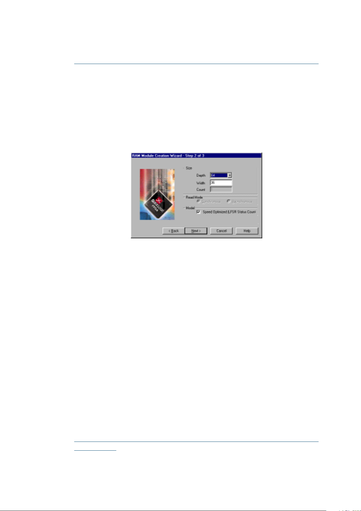
FIFOs may be created with the RAM/FIFO wizard in the QuickWorks tools. Figure 2 shows the
graphical interface used to create these FIFOs. FIFOs may be designed up to
1,024 words deep. The 22 RAM cells available in the QL5732 allow for up to:
• 11 FIFOs at 128 words deep (36 wide)
• 5 FIFOs at 256 words deep (36 wide)
• 2 FIFOs at 512 words deep (44 wide)
• 1 FIFO at 1,024 words deep (44 wide)
Figure 2: Graphical Interface to create FIFO
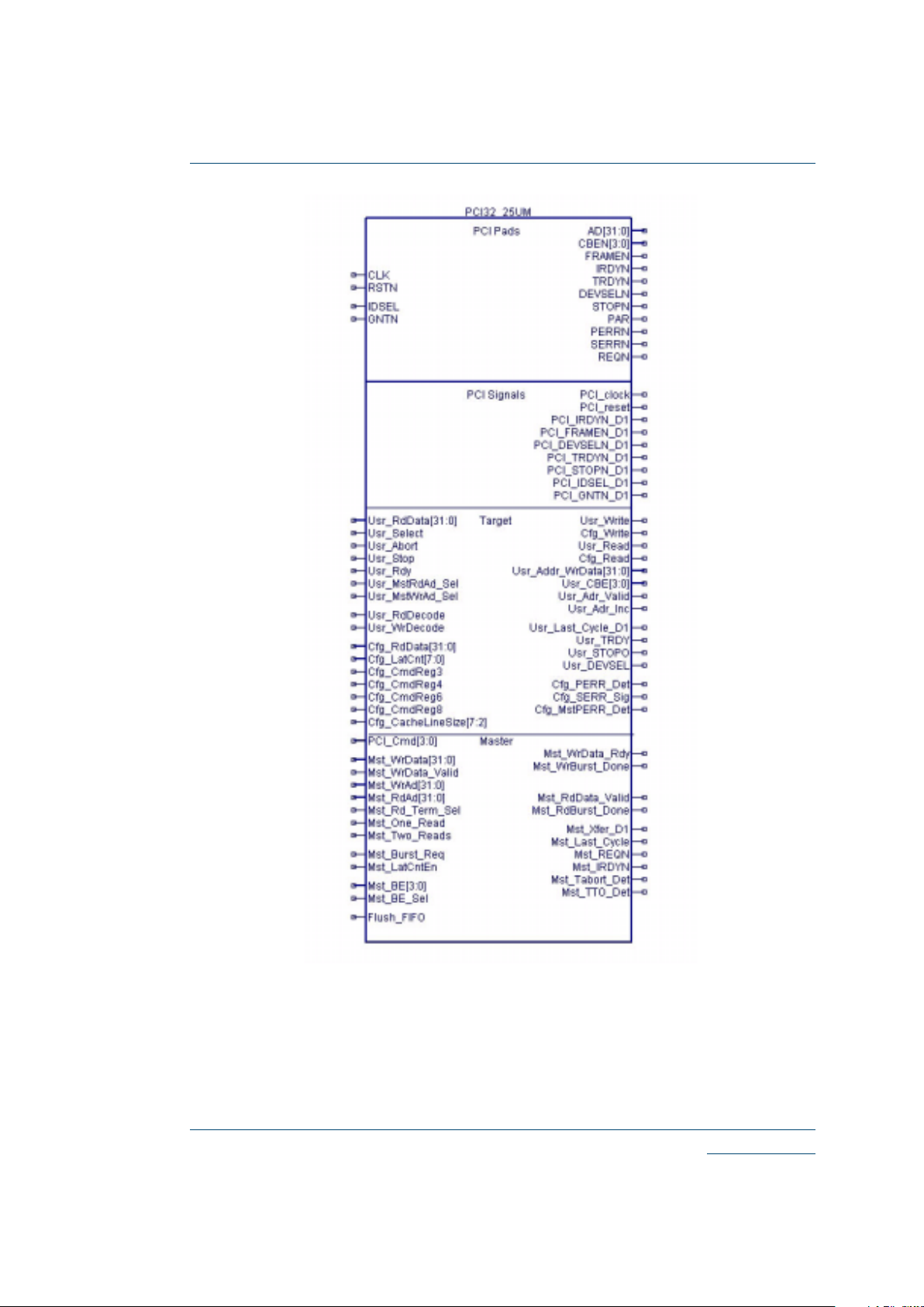
PCI Interface Symbol
Figure 2 shows the graphical interface symbol numbers you have to use in your schematic design
in order to attach the local interface programmable logic design to the PCI core. If you are
designing with a top-level Verilog or VHDL file you must use a structural instantiation of this
PCI32_25µm block (Figure 3) instead of a graphical symbol.
© 2003 QuickLogic Corporation
www.quicklogic.com
•
•
•
•
•
•
QL5732 Enhanced QuickPCI Device Data Sheet Rev C
5
Figure 3: PCI Interface Symbol
www.quicklogic.com
© 2003 QuickLogic Corporation
•
•
•
•
•
•
QL5732 Enhanced QuickPCI Device Data Sheet Rev C
6
PCI Master Interface
The internal signals used to interface with the PCI controller in the QL5732 are listed in Table 1
along with a description of each signal. The direction of the signal indicates if the signal is an input
provided by the local interface (I) or an output provided by the PCI controller (O).
NOTE: Signals that end with the character ‘N’ should be considered active-low (for example,
Mst_IRDYN).
Table 1: PCI Master Interface
Signal I/O Description
PCI_cmd[3:0] I PCI command to be used for the master transaction This signal must remain unchanged
throughout the period when Mst_Burst_Req is active. PCI commands considered as Reads include
Interrupt Acknowledge, I/O Read, Memory Read, Configuration Read, Memory Read Multiple,
and Memory Read Line. PCI commands considered as Writes include Special Cycle, I/O Write,
Memory Write, Configuration Write, Memory Write, and Invalidate.Users should make sure that
only valid PCI commands are supplied.
mst_burst_req I Request use of the PCI bus When it is active, the core requests the PCI bus and then generates
a Master transaction. This signal should be held active until all requested data is transferred on the
PCI bus and deactivated in the 2nd clock cycle following the last data transfer on PCI (to avoid
being considered as requesting a new transaction).
mst_wrAd[31:0] I Address for master DMA writes This address must be treated as valid from the beginning of a
DMA Write until the DMA Write operation is complete. It should be incremented by four bytes
each time data is transferred on the PCI bus.
mst_rdAd[31:0] I Address for master DMA reads This address must be treated as valid from the beginning of a
DMA read until the DMA Read operation is complete. It should be incremented by four bytes each
time data is transferred on the PCI bus.
Mst_WrData[31:0] I Data for master DMA Writes (to PCI bus)
Mst_BE[3:0] I Byte enables for master DMA Reads and writes Active-low.
Mst_WrData_Valid I Data and byte enable valid on Mst_W rData[31:0] (for master Write only) and Mst_BE[3:0] (for both
master Read and Write)
Mst_WrData_Rdy O Data receive acknowledge for Mst_WrData[31:0] (for master Write only) and
Mst_BE[3:0] (for both) This serves as the PUSH control for the internal FIFO and the POP
control for the external FIFO (in FPGA region) which provides data and byte enables to the PCI32
core.
Mst_BE_Sel I Byte enable select for master transactions When low, Mst_BE[3:0] should remain constant
throughout the entire transfer (when Mst_Burst_Req is active) and it is used for every data phase of
the master transaction. When high, Mst_BE[3:0] pushed into internal FIFO (along with data in case
of master Write) is used. Should be held constant throughout the transaction.
Mst_WrBurst_Done O Master Write transaction is completed Active for only one clock cycle.
Mst_Rd_Term_Sel I Master Read termination mode select when Mst_BE_Sel is high When both Mst_BE_Sel
and Mst_Rd_Term_Sel are high, Master Read termination happens when the internal FIFO is
empty, and Mst_Two_Reads and Mst_One_Read are ignored. When either signal is low,
Mst_Two_Reads and Mst_One_Read are used to signal the end of Master Read. Should be held
constant throughout the transaction.
Mst_One_Read I Signals to the PCI32 core that only one data transfer remains to be read in the burst Read.
© 2003 QuickLogic Corporation
www.quicklogic.com
•
•
•
•
•
•
QL5732 Enhanced QuickPCI Device Data Sheet Rev C
7
Mst_Two_Reads I Two data transfers remain to be read in the burst Read It is not used for single-data-phase
Master Read transactions.
Mst_RdData_Valid O Master Read data valid on Usr_Addr_WrData[31:0 ] This serves as the PUSH control for the
external FIFO (in FPGA region) that receives data from the PCI32 core.
Mst_RdBurst_Done O Master Read transaction is completed Active for only one clock cycle.
Flush_FIFO I Internal FIFO flush FIFO flushed immediately after it is active (synchronized with PCI clock).
Mst_LatCntEn I Enable Latency Counter Set to 0 to ignore the Latency Timer in the PCI configuration space
(offset 0Ch).
For full PCI compliance, this port should be always set to 1.
Mst_Xfer_D1 O Data was transferred on the previous PCI clock Useful for updating DMA transfer counts on
DMA Read operations
Mst_Last_Cycle O Active during the last data transfer of a master transaction
Mst_REQN O Copy of the PCI REQN signal generated by QL5732 as PCI master Not usually used in
the back-end design.
Mst_IRDYN O Copy of the PCI IRDYN signal generated by QL5732 as PCI master
Valid only when
QL5
732 is the PCI master. Kept low otherwise. Not usually used in the back-end design.
Mst_Tabort_Det O Target abort detected during master transaction This is normally an error condition handled
in the DMA controller.
Mst_TTO_Det O Target timeout detected (no response from target) This is normally an error condition
handled in the DMA controller.
Table 1: PCI Master Interface
Signal I/O Description
www.quicklogic.com
© 2003 QuickLogic Corporation
•
•
•
•
•
•
QL5732 Enhanced QuickPCI Device Data Sheet Rev C
8
PCI Target Interface
Table 2: PCI Target Interface
Signal I/O Description
Usr_Addr_WrData[31:0] O Target address, and target Write data
During all target accesses, the address is presented
on Usr_Addr_WrData[31:0]; at the same time, Usr_Adr_Valid is active. During target Write
transactions, this port also presents valid Write data to the PCI configuration space or user
logic when Usr_Adr_Inc is active.
Usr_CBE[3:0] O PCI command and byte enables During target accesses, the PCI command is presented on
Usr_CBE[3:0]; at the same time, Usr_Adr_Valid is active. This port also presents active-low
byte enables to the PCI configuration space or user logic.
Usr_Adr_Valid O Indicates the beginning of a PCI transaction, and that a target address is valid on
Usr_Addr_WrData[31:0] and the PCI command is valid on Usr_CBE[3:0]. When this signal is
active, the target address must be latched and decoded to determine if this address belongs to
the device's memory or I/O space. Also, the PCI command must be decoded to determine the
type of PCI transaction. On subsequent clocks of a target access, this signal is low, indicating
that address is NOT present on Usr_Addr_WrData[31:0].
Usr_Adr_Inc O Indicates that the target address should be incremented, because the pr evious data transfer has
completed. During burst target accesses, the target address is only presented to the back-end
logic at the beginning of the transaction (when Usr_Adr_V alid is active), and must therefore be
latched and incremented by four for subsequent data transfers. Note that during target Write
transactions, Usr_Adr_Inc indicates valid data on Usr_Addr_WrData[31:0] that must be
accepted by the backend logic (regardless of the state of Usr_Rdy). During Read transactions,
Usr_Adr_Inc signals to the backend that the PCI core has presented the read data on the PCI
bus (TRDYN asserted).
Usr_RdDecode I This signal should be the combinatorial decode of the "user read" command from
Usr_CBE[3:0]. This command may be mapped from any of the PCI Read commands, such as
Memory Read, Memory Read Line, Memory Read Multiple, I/O Read, etc. It is internally
gated with Usr_Adr_Valid.
Usr_WrDecode I This signal should be the combinatorial decode of the "user write" command from
Usr_CBE[3:0]. This command may be mapped from any of the PCI Write comma nds, such as
Memory Write or I/O Write. It is internally gated with Usr_Adr_Valid.
Usr_Select I This signal should be driven active when the address on Usr_Addr_WrData[31:0] has been
decoded and determined to be within the address space of the device. Usr_Addr_WrData[31:0]
must be compared to each of the valid Base Address Registers in the PCI configuration space.
Also, this signal must be gated by the Memory Access Enable or I/O Access Enable registers in
the PCI configuration space (Command Register bits 1 or 0 at offset 04h). Internally gated
with Usr_Adr_Valid.
Usr_Write O This signal is active throughout a "user write" transaction, which has been decoded by
Usr_WrDecode at the beginning of the transaction. The Write strobe for individual DWORDs
of data (on Usr_Addr_WrData[31:0]) during a user Write transaction should be generated by
logically ANDing this signal with Usr_Adr_Inc.
Cfg_Write O This signal is active throughout a "configuration write" transaction. The Write strobe for
individual DWORDs of data (on Usr_Addr_WrData[31:0]) during a configuration Write
transaction should be generated by logically ANDing this signal with Usr_Adr_Inc.
Usr_Read O This signal is active throughout a "user read" transaction, which has been decoded by
Usr_RdDecode at the beginning of the transaction.
Cfg_Read O This signal is active throughout a "configuration read" transaction.
© 2003 QuickLogic Corporation
www.quicklogic.com
•
•
•
•
•
•
QL5732 Enhanced QuickPCI Device Data Sheet Rev C
9
Cfg_RdData[31:0] I Data from the PCI configuration registers, required to be presented during PCI configuration
reads.
Usr_RdData[31:0] I Data from the back-end user logic required to be presented during PCI user reads.
Cfg_CmdReg3 I Bit 3 from the Command Register in the PCI configuration space (offset 04h). Enable Special
Cycle monitoring. If high, the core reports data parity error in Special Cycles through SERRN
if Cfg_CmdReg8 is active.
Cfg_CmdReg4 I Bit 4 from the Command Register in the PCI configuration space (offset 04h). Memory Write
and Invalidate (MWI) Enable. If high, the core generates MWI transactions as requested by the
backend. Otherwise it uses Memory Write instead even if MWI is requested.
Cfg_CmdReg6 I Bit 6 from the Command Register in the PCI configuration space (offset 04h). Parity Error
Response. If high, the core uses PERRN to report data parity errors. Otherwise it never drives
it.
Cfg_CmdReg8 I Bit 8 from the Command Register in the PCI configuration space (offset 04h). SERRN En able.
If high, the cores uses SERRN to report address parity errors if Cfg_CmdReg6 is high.
Cfg_LatCnt[7:0] I 8-bit value of the Latency Timer in the PCI configuration space (offset 0Ch).
Usr_MstRdAd_Sel I Used when a target Read operation should return the value set on the Mst_RdAd[31:0] pins.
This select pin saves on logic which would otherwise need to be used to multiplex
Mst_RdAd[31:0] into the Usr_RdData[31:0] bus. When this signal is asserted, the data on
Usr_RdData[31:0] is ignored.
Usr_MstWrAd_Sel I Used when a target read operation should return the value set on the Mst_WrAd[31:0] pins.
This select pin saves on logic which would otherwise need to be used to multiplex
Mst_WrAd[31:0] into the Usr_RdData[31:0] bus. When this signal is asserted, the data on
Usr_RdData[31:0] is ignored.
Cfg_PERR_Det O Parity error detected on the PCI bus. When this signal is active, bit 15 of the Status Register
must be set in the PCI configuration space (offset 04h).
Cfg_SERR_Sig O System error asserted on the PCI bus. When this signal is active, the Signalled System Error
bit, bit 14 of the Status Register, must be set in the PCI configuration space (offset 04h).
Cfg_MstPERR_Det O Data parity error detected on the PCI bus by the master . When this signal is active, bit 8 of the
Status Register must be set in the PCI configuration space (offset 04h).
Usr_TRDY O Inverted copy of the TRDYN signal as driven by the PCI target interface. Valid only within a
target access.
Usr_STOPO O Inverted copy of the STOPN signal as driven by the PCI target interface. Valid only within a
target access.
Usr_DEVSEL O Inverted copy of the DEVSELN signal as driven by the PCI target interface. Valid only within a
target access.
Usr_Last_Cycle_D1 O Active one clock cycle after the last data phase (may not with data transfer) occurs on PCI a nd
inactive one clock cycle afterwards.
Usr_Rdy I Used to delay (add wait states to) a target PCI transaction when the backend needs additional
time to provide data (read) or accept data (write). Subject to PCI latency restrictions.
Usr_Stop I Used to prematurely stop a PCI target access on the next PCI clock.
Usr_Abort I Used to signal Target Abort on PCI when the backend has fatal errors and is unable to
complete a transaction. Rarely used.
Table 2: PCI Target Interface
Signal I/O Description
www.quicklogic.com
© 2003 QuickLogic Corporation
•
•
•
•
•
•
QL5732 Enhanced QuickPCI Device Data Sheet Rev C
10
PCI Internal Signals
RAM Module Features
The QL5732 device has twenty-two 2,304-bit RAM modules, for a total of 50,668 RAM bits.
Using two “mode” pins, designers can configure each module into 128 × 18, 256 × 9, 512 × 4,
or 1024 × 2 blocks (see Figure 1). The blocks are also easily cascadable to increase their effective
width or depth.
The RAM modules are “dual-ported” with completely independent Read and Write ports and
separate Read and Write clocks. The Read ports support asynchronous and synchronous
operation, while the Write ports support synchronous operation. Each port has 18 data lines and
ten address lines, allowing word lengths of up to 18 bits and address spaces of up to 1,024 words.
Depending on the mode selected, however, some higher order data or address lines may not be
used.
The Write Enable (WE) line acts as a clock enable for synchronous Write operation. The Read
Enable (RE) acts as a clock enable for synchronous Read operation (ASYNCRD input low), or as
a flow-through enable for asynchronous Read operation (ASYNCRD input high).
Designers can cascade multiple RAM modules to increase the depth or width allowed in single
modules by connecting corresponding address lines together and dividing the words between
modules. This approach allows up to 1,024-deep configurations as large as 44 bits wide in the
QL5732 device.
A similar technique can be used to create depths greater than 1,024 words. In this case, address
signals higher than the eighth bit are encoded onto the write enable (WE) input for Write
operations. The Read data outputs are multiplexed together using encoded higher Read address
bits for the multiplexer SELECT signals.
Table 3: PCI Internal Signals
Signal Description
PCI_clock O PCI clock.
PCI_reset O PCI reset signal.
PCI_IRDYN_D1 O Copy of the IRDYN signal from the PCI bus, delayed by one clock.
PCI_FRAMEN_D1 O Copy of the FRAMEN signal from the PCI bus, delayed by one clock.
PCI_DEVSELN_D1 O Copy of the DEVSELN signal from the PCI bus, delayed by one
clock.
PCI_TRDYN_D1 O Copy of the TRDYN signal from the PCI bus, delayed by one clock.
PCI_STOPN_D1 O Copy of the STOPN signal from the PCI bus, delayed by one clock.
PCI_IDSEL_D1 O Copy of the IDSEL signal from the PCI bus, delayed by one clock.
© 2003 QuickLogic Corporation
www.quicklogic.com
•
•
•
•
•
•
QL5732 Enhanced QuickPCI Device Data Sheet Rev C
11
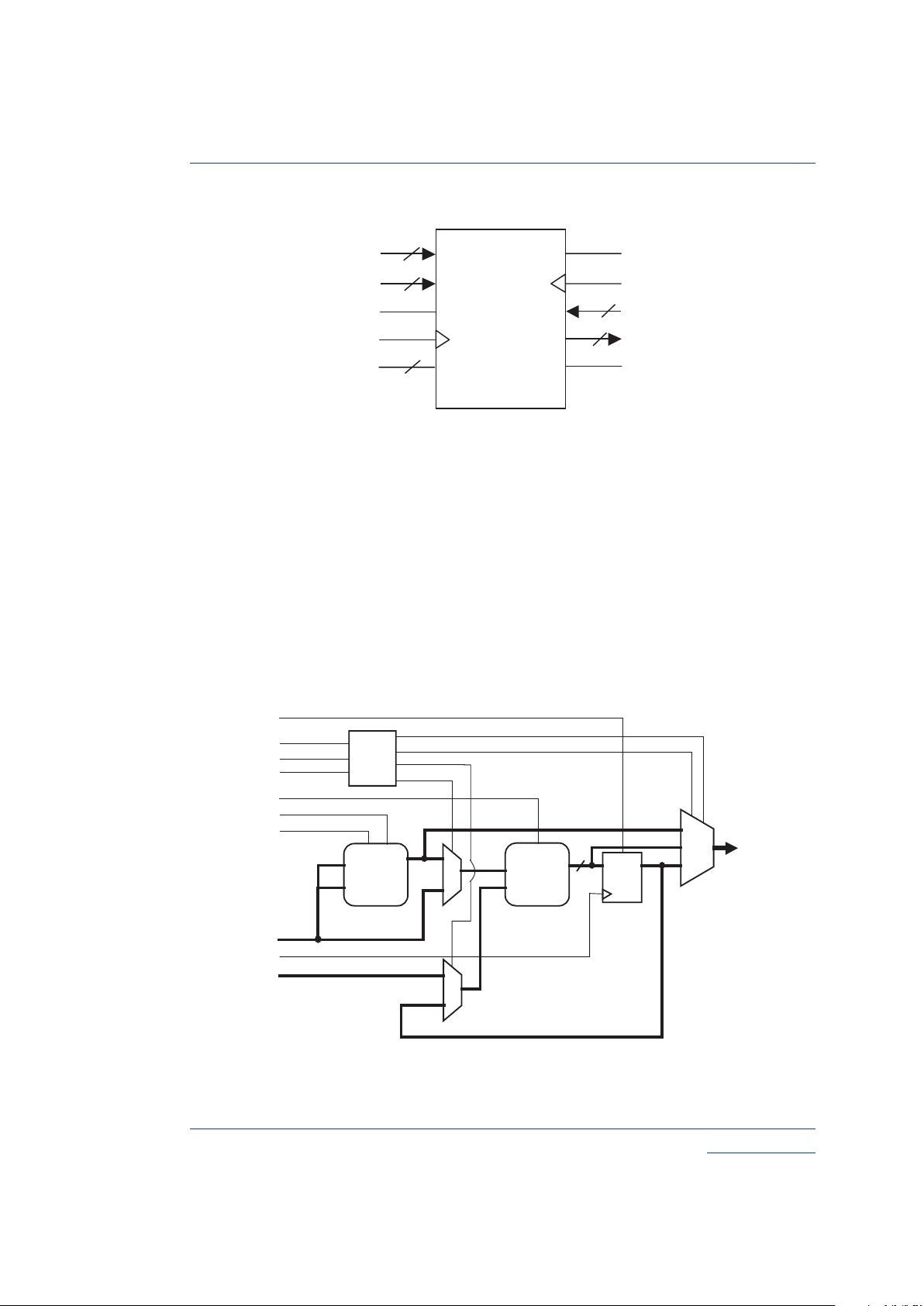
QL5732 Embedded Computational Unit (ECU)
T raditional Programmable Logic architectures do not implement arithmetic functions efficiently—
these functions require high logic cell usage while achieving only moderate performance results.
The QL5732 architecture allows for functionality above and beyond that achievable using
programmable logic devices. By embedding a dynamically reconfigurable computational unit, the
QL5732 device can address various arithmetic functions efficiently—this approach offers greater
performance than traditional programmable logic implementations. The embedded block is
implemented at the transistor level as shown in Figure 5.
Figure 5: ECU Block Diagram
The 12 QL5632 ECU blocks are placed next to the SRAM circuitry for efficient
memory/instruction fetch and addressing for DSP algorithmic implementations.
WA
WD
WE
WCLK
RE
RCLK
RA
RD
RAM
Module
[9:0]
[17:0]
[9:0]
[17:0]
MODE ASYNCRD
[1:0]
Figure 4: RAM Module
A
[0:15]
B
[0:15]
SIGN2
SIGN1
CIN
S1
S2
S3
A
B
C
D
3-4
decoder
8-bit
Multiplier
17 inc.
COUT
16-bit
Adder
17-bit
Register
2-1
mux
2-1
mux
3-1
mux
Q[0:1
6]
CLK
RESET
DQ
00
01
10A[0:7]
A[8:15]

www.quicklogic.com
© 2003 QuickLogic Corporation
•
•
•
•
•
•
QL5732 Enhanced QuickPCI Device Data Sheet Rev C
12
Twelve 8-bit MAC functions can be implemented per cycle for a total of
~1.2 billion MACs/s
when clocked at 98 MHz. Additional multiply-accumulate functions can be implemented in the
programmable logic.
The modes for the ECU block are dynamically re-programmable through the programmable logic.
Phase Locked Loop (PLL) Information
Instead of requiring extra components, designers simply need to instantiate one of the
pre-configured models (described in this section). The QuickLogic built-in PLLs support a wider
range of frequencies than many other PLLs. These PLLs also have the ability to be cascaded to
support different ranges of frequency multiplications or divisions, driving the device at a faster or
slower rate than the incoming clock frequency. Most importantly, they achieve a very short clockto-out time—generally less than 3 ns. This low clock-to-out time is achieved by the PLL
subtracting the clock tree delay through the feedback path, effectively making the clock tree delay
zero.
Figure 6
illustrates a typical QuickLogic ESP PLL.
Table 4: ECU Mode Select Criteria
Instruction
Operation
ECU Performance
a
, -B WCC
a. tPD, tSU and tCO do not include routing paths in/out of the ECU block.
S1 S2 S3
t
PD
t
SU
t
CO
0 0 0 Multiply 7.0 ns max
0 0 1 Multiply-Add
9.4
ns max
0 1 0 Accumulate
b
b. Internal feedback path in ECU restricts max clk frequency to 224 MHz.
4.1 ns
min
1.2 ns
max
0 1 1 Add
3.3
max
1 0 0 Multiply (registered)
c
c. B [15:0] set to zero.
NOTE: Timing numbers in Table 1 represent -B Worst Case
Commercial conditions.
10.2 ns
min
1.2 ns
max
1 0 1 Multiply- Add (registered)
10.2 ns
min
1.2 ns
max
1 1 0 Multiply - Accumulate
10.2 ns
min
1.2 ns
max
1 1 1 Add (registered)
4.1 ns
min
1.2 ns
max

© 2003 QuickLogic Corporation
www.quicklogic.com
•
•
•
•
•
•
QL5732 Enhanced QuickPCI Device Data Sheet Rev C
13
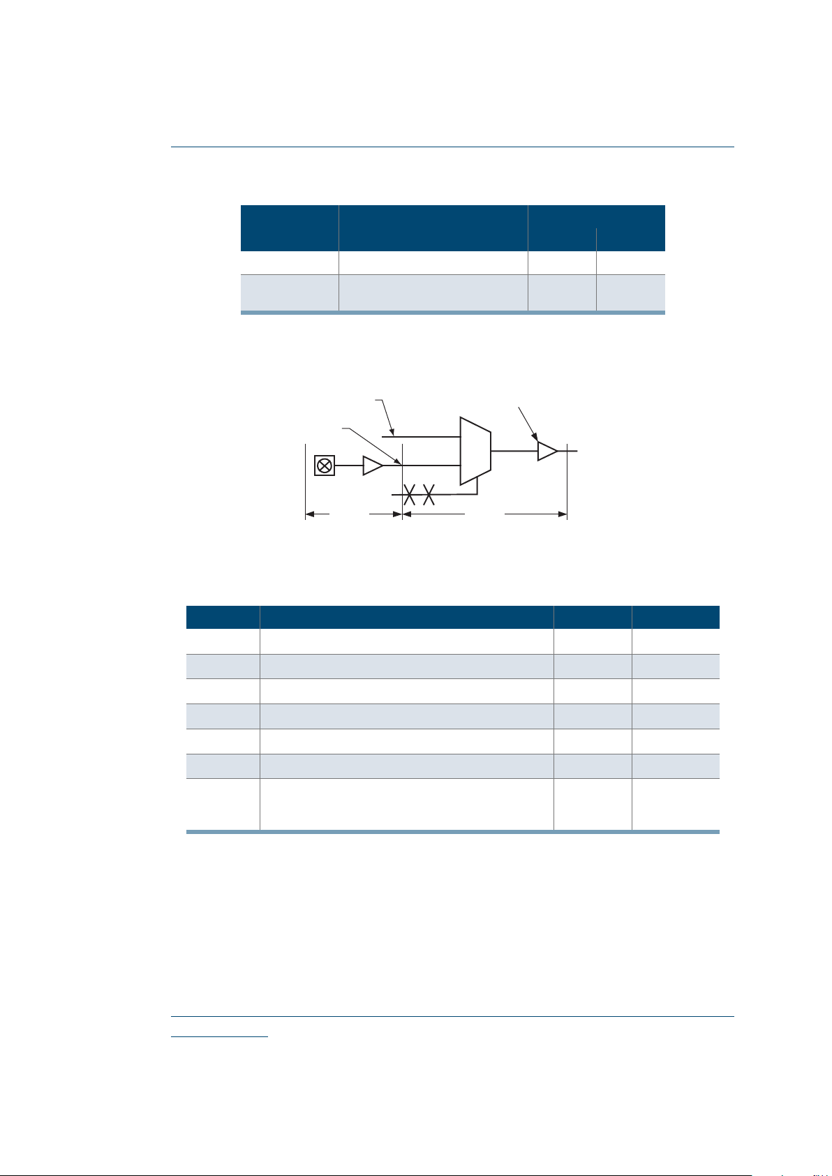
Figure 6: PLL Block Diagram
F
in
represents a very stable high-frequency input clock and produces an accurate signal reference.
This signal can either bypass the PLL entirely, thus entering the clock tree directly, or it can pass
through the PLL itself.
Within the PLL, a voltage-controlled oscillator (VCO) is added to the circuit. The external F
in
signal
and the local VCO form a control loop. The VCO is multiplied or divided down to the reference
frequency, so that a phase detector (the crossed circle in Figure 6) can compare the two signals.
If the phases of the external and local signals are not within the tolerance required, the phase
detector sends a signal through the charge pump and loop filter (Figure 6). The charge pump
generates an error voltage to bring the VCO back into alignment, and the loop filter removes any
high frequency noise before the error voltage enters the VCO. This new VCO signal enters the
clock tree to drive the chip's circuitry.
F
out
represents the clock signal emerging from the output pad (the output signal PLLPAD_OUT
is explained in Table 6). This clock signal is meaningful only when the PLL is configured for
external use; otherwise, it remains in high Z state, as shown in the post-simulation waveform.
Most QuickLogic products contain four PLLs. The PLL presented in Figure 6 controls the clock
tree in the fourth Quadrant of its ESP. QuickLogic PLLs compensate for the additional delay
created by the clock tree itself, as previously noted, by subtracting the clock tree delay through the
feedback path.
For more specific information on the Phase Locked Loops, please refer to Application Note 58
at
http://www.quicklogic.com/images/appnote58.pdf
PLL Modes of Operation
QuickLogic PLLs have eight modes of operation, based on the input frequency and desired output
frequency—Table 5 indicates the features of each mode.
vco
Filter
F
IN
F
OUT
+
-
1st Quadrant
2nd Quadrant
3rd Quadrant
4th Quadrant
Clock
Tree
Frequency Divide
Frequency Multiply
1
.
_
.
2
.
_
.
4
.
_
.
4
.
_
.
2
.
_
.
1
.
.
_

www.quicklogic.com
© 2003 QuickLogic Corporation
•
•
•
•
•
•
QL5732 Enhanced QuickPCI Device Data Sheet Rev C
14
NOTE: "HF" stands for "high frequency" and "LF" stands for "low frequency."
NOTE: The input frequency can range from 16 MHz to 300 MHz, while output frequency
ranges from 25 MHz to 250 MHz. When you add PLLs to y our top-lev el design, be sure
that the PLL mode matches your desired input and output frequencies.
PLL Signals
Table 6 summarizes the key signals in QuickLogic's PLLs.
NOTE: Because PLLCLK_IN and PLL_RESET signals have INPAD, and PLLPAD_OUT has
OUTPAD, you do not have to add additional pads to your design.
Table 5: PLL Mode Frequencies
PLL Model
Output
Frequency
Input Frequency Range Output Frequency Range
PLL_HF Same as input 66 MHz–150 MHz 66 MHz–150 MHz
PLL_LF Same as input 25 MHz–133 MHz 25 MHz–133 MHz
PLL_MULT2HF 2x 50 MHz–125 MHz 100 MHz–250 MHz
PLL_MULT2LF 2x 16 MHz–50 MHz 32 MHz–100 MHz
PLL_DIV2HF 1/2x 100 MHz–250 MHz 50 MHz–125 MHz
PLL_DIV2LF 1/2x 50 MHz–100 MHz 25 MHz–50 MHz
PLL_MULT4 4x 16 MHz–40 MHz 64 MHz–160 MHz
PLL_DIV4 1/4x 100 MHz–300 MHz 25 MHz–75 MHz
Table 6: PLL Signals
Signal Name Description
PLLCLK_IN Input clock signal
PLL_RESET
Active High Reset If PLL_RESET is asserted, then CLKNET_OUT and
PLLPAD_OUT are reset to 0. This signal must be asserted and then released
in order for the LOCK_DETECT to work.
ONn_OFFCHIP
PLL output This signal selects whether the PLL will drive the internal clock
network or be used off-chip. This is a static signal, not a dynamic signal.
Tied to GND = outgoing signal drives internal gates.
Tied to VCC = outgoing signal used off-chip.
CLKNET_OUT
Out to internal gates This signal bypasses the PLL logic before driving the
internal gates. Note that this signal cannot be used in the same quadrant where
the PLL signal is used (PLLCLK_OUT).
PLLCLK_OUT
Out from PLL to internal gates This signal can drive the internal gates after
going through the PLL. For this to work, ONn_OFFCHIP must be tied to GND.
PLLPAD_OUT
Out to off-chip This outgoing signal is used off-chip. For this to work,
ONn_OFFCHIP signal must be tied to VCC.
LOCK_DETECT
Active High Lock detection signal NOTE: For simulation purposes, this
signal gets asserted after 10 clock cycles. However, it can take a maximum of
200 clock cycles to sync with the input clock upon release of the RESET signal.

© 2003 QuickLogic Corporation
www.quicklogic.com
•
•
•
•
•
•
QL5732 Enhanced QuickPCI Device Data Sheet Rev C
15
Joint Test Access Group (JTAG) Support
Figure 7: JTAG Block Diagram
JTAG pins support the IEEE Standard 1149.1a to provide boundary scan capability for the
QL5732 device. Six pins are dedicated to JTAG and programming functions on each QL5732
device; these pins are unavailable for general design input and output signals. TDI, TDO, TCK,
TMS, and TRSTB are JTAG pins. The sixth pin, STM, is used only for programming.
Microprocessors and Application Specific Integrated Circuits (ASICs) pose many design
challenges, on problem being the accessibility of test points. JTAG was formed in response to this
challenge, resulting in IEEE standard 1149.1, the Standard T est Access Port and Boundary Scan
Architecture.
The JTAG boundary scan test methodology allows complete observation and control of the
boundary pins of a JTAG-compatible device through JTAG software. A Test Access Port (TAP)
controller works in concert with the Instruction Register (IR); these allow users to run three
required tests, along with several user-defined tests.
JTAG tests allow users to reduce system debug time, reuse test platforms and tools, and reuse
subsystem tests for fuller verification of higher level system elements.
The JTAG 1149.1 standard requires the following three tests:
TCK
TMS
TRSTB
RDI
TDO
Instruction Decode
&
Control Logic
TAp Controller
State Machine
(16 States)
Instruction Register
Boundary-Scan Register
(Data Register)
Mux
Bypass
Register
Mux
Internal
Register
I/O Registers
User Defined Data Register

www.quicklogic.com
© 2003 QuickLogic Corporation
•
•
•
•
•
•
QL5732 Enhanced QuickPCI Device Data Sheet Rev C
16
• Extest Instruction. The Extest instruction per forms a PCB interconnect test. This test
places a device into an external boundary test mode, selecting the boundary scan register to
be connected between the T AP's T est Data In (TDI) and T est Data Out (TDO) pins. Boundary
scan cells are preloaded with test patterns (via the Sample/Preload Instruction), and input
boundary cells capture the input data for analysis.
• Sample/Preload Instruction. This instruction allows a device to remain in its functional
mode, while selecting the boundary scan register to be connected between the TDI and TDO
pins. For this test, the boundary scan register can be accessed via a data scan operation,
allowing users to sample the functional data entering and leaving the device.
• Bypass Instruction. The Bypass instruction allows data to skip a device's boundary scan
entirely, so the data passes through the bypass register. The Bypass instruction allows users
to test a device without passing through other devices. The bypass register connects the TDI
and TDO pins, allowing serial data to be transferred through a device without affecting the
operation of the device.
Development Tool Support
Software support for the QL5732 device is available through the QuickWorks development
package. This turnkey PC-based QuickWorks package, shown in Figure 8, provides a complete
ESP software solution with design entry, logic synthesis, place and route, and simulation.
QuickWorks includes VHDL, Verilog, schematic, and mixed-mode entry with fast and efficient
logic synthesis provided by the integrated Synplicity Synplify Lite tool, specially tuned to take
advantage of the QL5732 architecture. QuickWorks also provides functional and timing
simulation for guaranteed timing and source-level debugging.
The UNIX-based QuickTools package is a subset of QuickWorks and provides a solution for
designers who use schematic-only design flow third-party tools for design entry, synthesis, or
simulation. QuickTools Reads EDIF netlists and provides support for all QuickLogic devices.
QuickTools also supports a wide range of third-party modeling and simulation tools.
Figure 8: QuickWorks Tool Suite
Schematic
Schematic
Turbo
HDL Editor
Third Party
Design Entry
& Synthesis
Third Party
Simulation
VHDL/
VHDL/
Verilog
Verilog
SCS
Tools
Silos III
Simulator
Optimize, Place,
Route
Mixed-Mode Design
Mixed-Mode Design
Synplify-Lite
HDL
Synthesis
QuickWorks Design Software
Aldec

© 2003 QuickLogic Corporation
www.quicklogic.com
•
•
•
•
•
•
QL5732 Enhanced QuickPCI Device Data Sheet Rev C
17
Electrical Specifications
Table 7: Absolute Maximum Ratings
VCC Voltage -0.5 V to 3.6 V DC Input Current ±20 mA
V
CCIO
Voltage -0.5 V to 4.6 V ESD Pad Protection ±2000 V
V
REF
Voltage 2.7 V
Leaded Package
Storage Temperature
-65°C to +150°C
Input Voltage
-0.5 V to V
CCIO
+0.5 VLaminate Package (BGA)
Storage Temperature
-55°C to +125°C
Table 8: Operating Range
Symbol Parameter
Military Industrial Commercial
Min Max Min Max Min Max
V
CC
Supply Voltage
I/O Input Tolerance Voltage
Ambient Temperature
Case Temperature
2.3 V 2.7 V 2.3 V 2.7 V 2.3 V 2.7 V
V
CCIO
2.3 V 3.6 V 2.3 V 3.6 V 2.3 V 3.6 V
TA -55°C -40°C 85 °C 0°C 70°C
TC - 125°C - - - -
K Delay Factor -B Speed Grade 0.42 1.35 0.43 1.26 0.46 1.23

www.quicklogic.com
© 2003 QuickLogic Corporation
•
•
•
•
•
•
QL5732 Enhanced QuickPCI Device Data Sheet Rev C
18
DC Characteristics
Table 10: DC Input and Output Levels
NOTE: The data provided in Table 10 are JEDEC and PCI Specifications—QuickLogic
devices either meet or exceed these requirements.
NOTE: All CLK and IOCTRL pins are clamped to the Vcc rail, not the V
ccio
. Therefore,
these pins can only be driven up to V
cc
+ 0.3 V.
Table 9: DC Characteristics
Symbol Parameter Conditions
Temperature
Min Max
I
I
I or I/O Input Leakage Current VI = V
CCIO
or GND -10 µA 10 µA
I
OZ
3-State Output Leakage Current VI = V
CCIO
or GND -10 µA 10 µA
C
I
Input Capacitance
a
a. Capacitance is sample tested only. Clock pins are 12 pF maximum.
--8 pF
I
OS
Output Short Circuit Current
b
b. Only one output at a time. Duration should not exceed 30 seconds.
Vo = GND
V
o
= V
CC
-15 mA
40 mA
-180 mA
210 mA
I
CC
D.C. Supply Current VI,V
o = VCCIO
or GND 0.50 mA(typ) 2 mA
I
CCIO
D.C. Supply Current on V
CCIO
- 0 mA 2 mA
I
CCIO
(DIF)
D.C. Supply Current on V
CCIO
for Differential I/O
---
I
REF
D.C. Supply Current on V
REF
- -10 µA 10 µA
I
PD
Pad Pull-down (programmable) V
CCIO
= 3.6 V - 150 µA
INREF V
IL
V
IH
V
OL
V
OH
I
OLIOH
V
MINVMAXVMIN
V
MAX
V
MIN
V
MAX
V
MAX
V
MIN
mA mA
LVTTL n/a n/a -0.3 0.8 2.0 V
CCIO
+ 0.3 0.4 2.4 2.0 -2.0
LVCMOS
2
n/a n/a -0.3 0.7 1.7 V
CCIO
+ 0.3 0.7 1.7 2.0 -2.0
GTL+ 0.88 1.12 -0.3 INREF
- 0.2 INREF + 0.2 V
CCIO
+ 0.3 0.6 n/a 40 n/a
PCI n/a n/a -0.3 0.3 x V
CCIO
0.5 x V
CCIO
V
CCIO
+ 0.5 0.1 x V
CCIO
0.9 x V
CCIO
1.5 -0.5
SSTL2 1.15 1.35 -0.3
INREF
-
0.18
INREF
+ 0.18 V
CCIO
+ 0.3 0.74 1.76 7.6 -7.6
SSTL3 1.3 1.7 -0.3 INREF - 0.2 INREF + 0.2 V
CCIO
+ 0.3 1.10 1.90 8 -8

© 2003 QuickLogic Corporation
www.quicklogic.com
•
•
•
•
•
•
QL5732 Enhanced QuickPCI Device Data Sheet Rev C
19
AC Characteristics
The AC characteristics are calculated at 2.5 V, T A = 25°C (K = 0.74). T o calculate delays, multipl y
the appropriate K factor in Table 8 by the numbers presented in Table 11 through Table 17.
Figure 9: Logic Cell
Table 11: Logic Cells
Symbol
Parameter
Value
Logic Cells Min Max
t
PD
Combinatorial Delay of the longest path: time taken by th e combinatorial circuit to
output
- 0.257 ns
t
SU
Setup time: time the synchronous input of the flip flop must be stable before the
active
clock edge
0.22 ns -
t
HL
Hold time: time the synchronous input of the flip flop must be stable after the active
clock edge
0-
t
CO
Clock to out delay: the amount of time taken by the flip flop to output after the
active clock edge.
- 0.255 ns
t
CWHI
Clock High Time: required minimum time the clock stays high 0.46 ns -
t
CWLO
Clock Low Time: required minimum time that the clock stays low 0.46 ns -
t
SET
Set Delay: time between when the flip flop is ”set” (high)
and when the output is consequently “set” (high)
- 0.18 ns
t
RESET
Reset Delay: time between when the flip flop is ”reset” (low) and when the output
is consequently “reset” (low)
- 0.09 ns
t
SW
Set Width: time that the SET signal remains high/low 0.3 ns -
t
RW
Reset Width: time that the RESET signal remains high/low 0.3 ns -
SET
D
CLK
RESET
Q

www.quicklogic.com
© 2003 QuickLogic Corporation
•
•
•
•
•
•
QL5732 Enhanced QuickPCI Device Data Sheet Rev C
20
Figure 10: Logic Cell Flip Flop Timing—First Waveform
Figure 11: Logic Cell Flip Flop Timing—Second Waveform
SET
RESET
Q
CLK
t
CWHI
(min)
t
CWLO
(min)
t
RESET
t
RW
t
SET
t
SW
CLK
D
Q
t
SU
t
HL
t
CO

© 2003 QuickLogic Corporation
www.quicklogic.com
•
•
•
•
•
•
QL5732 Enhanced QuickPCI Device Data Sheet Rev C
21
Figure 12: RAM Module
Table 12: RAM Cell Synchronous Write Timing
Symbol Parameter: RAM Cell Synchronous Write Timing
Value
Min
t
SWA
WA se tup time to WCLK: the amount of time the Write ADDRESS must be stable
before the active edge of the Write CLOCK
0.675 ns
t
HWA
WA hold time to WCLK: the amount of time the Write ADDRESS must be stable
after the active edge of the Write CLOCK
0 ns
t
SWD
WD setup time to WCLK: the amount of time the Write DA T A must be stable before
the active edge of the Write CLOCK
0.654 ns
t
HWD
WD hold time to WCLK: the amount of time the Write DATA must be stable after
the active edge of the Write CLOCK
0 ns
t
SWE
WE setup time to WCLK: the amount of time the Write ENABLE must be stable
before the active edge of the Write CLOCK
0.623 ns
t
HWE
WE hold time to WCLK: the amount of time the Write ENABLE mu st be stable after
the active edge of the Write CLOCK
0 ns
t
WCRD
WCLK to RD (WA=RA): the amount of time between the active W rite CLOCK edge
and the moment when the data is available at RD
-
WA
WD
WE
WCLK
RE
RCLK
RA
RD
RAM
Module
[9:0]
[17:0]
[9:0]
[17:0]
MODE ASYNCRD
[1:0]

www.quicklogic.com
© 2003 QuickLogic Corporation
•
•
•
•
•
•
QL5732 Enhanced QuickPCI Device Data Sheet Rev C
22
Figure 13: RAM Cell Synchronous Write Timing
Figure 14: RAM Cell Synchronous & Asynchronous Read Timing
t
SWA
t
SWD
t
SWE
t
HWA
t
HWD
t
HWE
t
WCRD
old data
new data
WCLK
WA
WD
WE
RD
t
SRA
t
HRA
RCLK
RA
t
SRE
t
HRE
t
RCRD
old data
new data
RE
RD
r
PDRD

© 2003 QuickLogic Corporation
www.quicklogic.com
•
•
•
•
•
•
QL5732 Enhanced QuickPCI Device Data Sheet Rev C
23
Table 13: RAM Cell Synchronous & Asynchronous Read Timing
Symbol Parameter: RAM Cell Synchronous Read Timing
Value
Min Max
t
SRA
RA setup time to RCLK: time the Read ADDRESS must be stable before the active
edge of the Read CLOCK
0.686 ns -
t
HRA
RA hold time to RCLK: time the Read ADDRESS must be stable after the active
edge of the Read CLOCK
0 ns -
t
SRE
RE setup time to WCLK: time the Read ENABLE must be stable before the active
edge of the Read CLOCK
0.243 ns -
t
HRE
RE hold time to WCLK: time the Read ENABLE must be stable after the active edge
of the Read CLOCK
0 -
t
RCRD
RCLK to RD: time between the active Read CLOCK edge and the time when the
data is available at RD
- 4.38 ns
RAM Cell Asynchronous Read Timing
r
PDRD
RA to RD: time between when the Read ADDRESS is input and when the DATA
is output
- 2.06 ns
Table 14: Input Register Cell
Symbol Parameter: Input Cell Register Only
Value
Min Max
t
ISU
Input register setup time: time the synchronous input of the flip flop must be stable
before the active clock edge
3.12 ns -
t
IHL
Input register hold time: time the synchronous input of the flip flop must be stable
after the active clock edge
0 ns -
t
ICO
Input register clock to out: time taken by the flip flop to outpu t after the active clock
edge
- 1.08 ns
t
IRST
Input register reset delay: time between when the flip flop is “reset”(low) and whe n
the output is consequently “reset” (low)
- 0.99 ns
t
IESU
Input register clock enable setup time: time “enable” must be stable before the
active clock edge
0.37 ns -
t
IEH
Input register clock enable hold time: time “enable” must be stable after the active
clock edge
0 ns -

www.quicklogic.com
© 2003 QuickLogic Corporation
•
•
•
•
•
•
QL5732 Enhanced QuickPCI Device Data Sheet Rev C
24
Figure 15: Input Register Cell
Table 15: Standard Input Delays
Symbol Parameter Value
Standard Input Delays To get the total input delay add this delay to tISU Min Max
t
SID(LVTTL)
LVTTL input delay: Low Voltage TTL for 3.3V applications - 0.34 ns
t
SID(LVCMOS2)
LVCMOS2 input delay: Low Voltage CMOS for 2.5V and lower
applications
- 0.42 ns
t
SID(GTL+)
GTL+ input delay: Gunning Transceiver Logic - 0.68 ns
t
SID(SSTL3)
SSTL3 input delay: Stub Series Terminated Logic for 3.3V - 0.55 ns
t
SID(SSTL2)
SSTL2 input delay: Stub Series Terminated Logic for 2.5V - 0.61 ns
R
CLK
D
Q
t
ISU
t
IHL
t
ICO
t
IESU
t
IEH
t
IRST
E

© 2003 QuickLogic Corporation
www.quicklogic.com
•
•
•
•
•
•
QL5732 Enhanced QuickPCI Device Data Sheet Rev C
25
Figure 16: Input Register Cell Timing
Figure 17: Global Clock Structure
Table 16: Eclipse Clock Performance
Clock Parameters
Clock Performance
Global Dedicated
Logic Cells (Internal) Clock signal generated internally 1.51 ns (max) 1.59 ns (max)
I/O’s (External) Clock signal generated externally 2.06 ns (max) 1.73 ns (max)
R
CLK
D
Q
t
ISU
t
IHL
t
ICO
t
IESU
t
IEH
t
IRST
E
Quad net
www.quicklogic.com
© 2003 QuickLogic Corporation
•
•
•
•
•
•
QL5732 Enhanced QuickPCI Device Data Sheet Rev C
26
Figure 18: Global Clock Structure Schematic
Table 17: QL5732 Global Clock Performance
Clock Segment Parameter
Value
Min Max
t
PGCK
Global clock pin delay to quad net - 1.34 ns
t
BGCK
Global clock buffer delay (quad net
to flip flop)
- 0.56 ns
Table 18: Output Register Cell
Symbol Parameter: Output Register Cell Only Min Max
t
OUTLH
Output Delay low to high (90% of H)
-0.40
t
OUTHL
Output Delay high to low (10% of L)
- 0.55
t
PZH
Output Delay tri-state to high (90% of H)
-2.94
t
PZL
Output Delay tri-state to low (10% of L)
- 2.34
t
PHZ
Output Delay high to tri-State
-3.07
t
PLZ
Output Delay low to tri-State
- 2.53
t
COP
Clock to out delay (does not include clock tree delays)
-
3.15 (fast slew)
10.2 (slow
slew)
Programmable Clock
External Clock
Global Clock Buffer
Global Clock
tPGCK tBGCK

© 2003 QuickLogic Corporation
www.quicklogic.com
•
•
•
•
•
•
QL5732 Enhanced QuickPCI Device Data Sheet Rev C
27
Figure 19: Output Register Cell
Figure 20: Output Register Cell Timing
Table 19: Output Slew Rates @ VCCIO = 3.3 V
Fast Slew Slow Slew
Rising Edge 2.8 V/ns 1.0 V/ns
Falling Edge 2.86 V/ns 1.0 V/ns
PAD
OUTPUT
REGISTER
L
H
L
H
t
OUTLH
t
OUTHL
L
H
Z
t
PZH
L
H
Z
t
PZL
L
H
Z
t
PLZ
L
H
Z
t
PHZ

www.quicklogic.com
© 2003 QuickLogic Corporation
•
•
•
•
•
•
QL5732 Enhanced QuickPCI Device Data Sheet Rev C
28
Figure 21: Loads for t
PXZ
Pin Type Descriptions
The QL5732 Device Pins are indicated in Table 21. Some of the pins presented in this table
connect to the PCI bus, and others are programmable as user I/O.
Table 20: Output Slew Rates @ V
CCIO
= 2.5 V
Fast Slew Slow Slew
Rising Edge 1.7 V/ns 0.6 V/ns
Falling Edge 1.9 V/ns 0.6 V/ns
Table 21: Pin Descriptions
Pin Function Description
TDI/RSI
Test Data In for JTAG /RAM
init. Serial Data In
Hold HIGH during normal operation. Connects to serial PROM
data in for RAM initialization. Connect to V
CC
if unused
TRSTB/RRO
Active low Reset for JTAG
/RAM init. reset out
Hold LOW during normal operation. Connects to serial PROM
reset for RAM initialization. Connect to GND if unused
TMS Test Mode Select for JTAG
Hold HIGH during normal operation. Connect to V
CC
if not used
for JTAG
TCK Test Clock for JTAG
Hold HIGH or LOW during normal operation. Connect to VCC or
ground if not used for JTAG
TDO/RCO
Test data out for JTAG /RAM
init. clock out
Connect to serial PROM clock for RAM initialization. Must be left
unconnected if not used for JTAG or RAM initialization
I/GCLK
High-drive input and/or global
clock network driver
Can be configured as either input or global clock
I/O Input/Output pin Can be configured as an input and/or output
V
CC
Power supply pin Connect to 2.5 V supply
V
CCIO<PCI>
Input voltage tolerance pin Connect to 3.3 V supply
V
CCIO<A>-<E>
Input voltage tolerance pin
Connect to 3.3 V supply if 3.3 V input tolerance is required;
otherwise, connect to 2.5 V supply
GND Ground pin Connect to ground
1K Ohms
t
PHZ
5pF
1K Ohms
5pF
t
PLZ

© 2003 QuickLogic Corporation
www.quicklogic.com
•
•
•
•
•
•
QL5732 Enhanced QuickPCI Device Data Sheet Rev C
29
PLLIN PLL clock input Clock input for PLL
DEDCLK Dedicated clock pin Low skew global clock
GNDPLL Ground pin for PLL Connect to GND
INREF
Differential reference voltage
Connect to reference voltage or ground if used for non-differential
input
PLLOUT PLL output pin Dedicated PLL output pin. Otherwise may be left unconnected
IOCTRL
Highdrive input
Can be used as highdrive input or clock to I/O register within the
same bank. Tied low or high if unused
Table 21: Pin Descriptions
Pin Function Description
www.quicklogic.com
© 2003 QuickLogic Corporation
•
•
•
•
•
•
QL5732 Enhanced QuickPCI Device Data Sheet Rev C
30
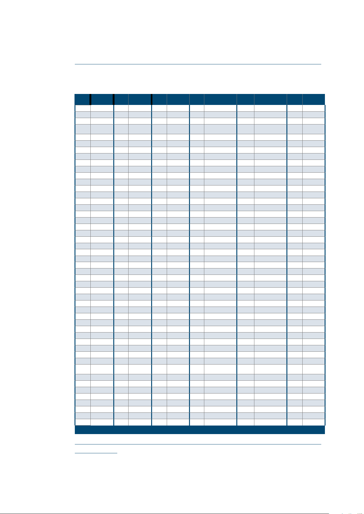
484 PBGA Pinout Table
Table 22: 484 PBGA Pinout Table
484
PBGA
Function
484
PBGA
Function
484
PBGA
Function
484
PBGA
Function
484
PBGA
Function
484
PBGA
Function
A1
I/O<A>
C17
I/O<G>
F11
VCCIO<H>
J5
I/O<A>
L21
I/O<F>
P15
VCC
A2
PLLRST<3>
C18
AD[18]
F12
VCCIO<G>
J6
I/O<A>
L22
I/O<F>
P16
I/O<E>
A3
I/O<A>
C19
AD[23]
F13
AD[12]
J7
I/O<A>
M1
I/O<B>
P17
I/O<E>
A4
I/O<A>
C20
GNDPLL<0>
F14
VCCIO<PCI
>
J8
VCC
M2
I/O<B>
P18
I/O<E>
A5
I/O<A>
C21
AD[27]
F15
N/C
J9
GND
M3
I/O<B>
P19
I/O<E>
A6
I/O<H>
C22
AD[30]
F16
VCCIO<G>
J10
VCC
M4
CLK<3>/PLLIN<1>
P20
I/O<E>
A7
I/O<H>
D1
I/O<A>
F17
N/C
J11
VCC
M5
I/O<B>
P21
I/O<E>
A8
IOCTRL<H>
D2
I/O<A>
F18
GNTN
J12
GND
M6
VCCIO<B>
P22
I/O<E>
A9
AD[0]
D3
I/O<A>
F19
REQN
J13
VCC
M7
CLK<1>
R1
I/O<B>
A10
N/C
D4
I/O<A>
F20
IOCTRL<F>
J14
GND
M8
VCC
R2
INREF<B>
A11
N/C
D5
I/O<A>
F21
I/O<F>
J15
VCC
M9
VCC
R3
I/O<B>
A12
TCK
D6
I/O<H>
F22
IOCTRL<F>
J16
AD[29]
M10
GND
R4
I/O<B>
A13
AD[10]
D7
I/O<H>
G1
I/O<A>
J17
VCCIO<F>
M11
GND
R5
I/O<B>
A14
AD[13]
D8
I/O<H>
G2
I/O<A>
J18
I/O<F>
M12
GND
R6
I/O<B>
A15
SERRN
D9
I/O<H>
G3
I/O<A>
J19
I/O<F>
M13
GND
R7
I/O<B>
A16
I/O<G>
D10
AD[4]
G4
I/O<A>
J20
I/O<F>
M14
GND
R8
GND
A17
IRDYN
D11
AD[7]
G5
I/O<A>
J21
I/O<F>
M15
GND
R9
VCC
A18
AD[17]
D12
AD[8]
G6
I/O<A>
J22
I/O<F>
M16
GND
R10
VCC
A19
AD[20]
D13
AD[14]
G7
GND
K1
TDI
M17
I/O<E>
R11
GND
A20
GND
D14
CBEN[1]
G8
I/O<H>
K2
I/O<A>
M18
I/O<E>
R12
VCC
A21
PLLOUT<3>
D15
IOCTRL<G>
G9
I/O<H>
K3
I/O<A>
M19
I/O<E>
R13
VCC
A22
IDSEL
D16
CBEN[2]
G10
I/O<H>
K4
I/O<A>
M20
CLK<7>
R14
VCC
B1
I/O<A>
D17
AD[16]
G11
CBEN[0]
K5
I/O<A>
M21
CLK<5>/PLLIN<3>
R15
GND
B2
GND
D18
AD[22]
G12
GND
K6
VCCIO<A>
M22
TMS
R16
I/O<D>
B3
GNDPLL<3>
D19
VCCPLL<0>
G13
I/O<G>
K7
I/O<A>
N1
I/O<B>
R17
VCCIO<E>
B4
GND
D20
AD[26]
G14
I/O<G>
K8
VCC
N2
I/O<B>
R18
I/O<E>
B5
I/O<A>
D21
AD[31]
G15
PAR
K9
VCC
N3
I/O<B>
R19
I/O<E>
B6
I/O<H>
D22
RSTN
G16
GND
K10
GND
N4
I/O<B>
R20
I/O<E>
B7
I/O<H>
E1
IOCTRL<A>
G17
VCCIO<F>
K11
GND
N5
I/O<B>
R21
I/O<E>
B8
INREF<H>
E2
I/O<A>
G18
I/O<F>
K12
GND
N6
I/O<B>
R22
I/O<E>
B9
I/O<H>
E3
I/O<A>
G19
I/O<F>
K13
GND
N7
I/O<B>
T1
I/O<B>
B10
AD[3]
E4
I/O<A>
G20
I/O<F>
K14
VCC
N8
VCC
T2
I/O<B>
B11
AD[6]
E5
I/O<A>
G21
INREF<F>
K15
VCC
N9
VCC
T3
I/O<B>
B12
N/C
E6
I/O<H>
G22
I/O<F>
K16
I/O<F>
N10
GND
T4
I/O<B>
B13
N/C
E7
N/C
H1
I/O<A>
K17
I/O<F>
N11
GND
T5
I/O<B>
B14
N/C
E8
I/O<H>
H2
I/O<A>
K18
I/O<F>
N12
GND
T6
VCCIO<B>
B15
I/O<G>]
E9
I/O<H>
H3
I/O<A>
K19
I/O<F>
N13
GND
T7
GND
B16
DEVSELN
E10
AD[5]
H4
I/O<A>
K20
I/O<F>
N14
VCC
T8
I/O<C>
B17
FRAMEN
E11
VCC
H5
IOCTRL<A>
K21
I/O<F>
N15
VCC
T9
N/C
B18
AD[19]
E12
AD[9]
H6
VCCIO<A>
K22
I/O<F>
N16
I/O<E>
T10
TRSTB
B19
PLLRST<0>
E13
AD[15]
H7
I/O<H>
L1
CLK<4>DEDCLK/
PLLIN<0>
N17
VCCIO<E>
T11
GND
B20
CBEN[3]
E14
AD[13]
H8
GND
L2
CLK<0>
N18
I/O<E>
T12
N/C
B21
AD[24]
E15
IOCTRL<G>
H9
VCC
L3
CLK<2>/PLLIN<2>
N19
I/O<E>
T13
I/O<D>
B22
AD[28]
E16
STOPN
H10
VCC
L4
I/O<A>
N20
I/O<E>
T14
N/C
C1
I/O<A>
E17
INREF<G>
H11
VCC
L5
I/O<A>
N21
I/O<E>
T15
I/O<D>
C2
I/O<A>
E18
I/O<G>
H12
GND
L6
I/O<A>
N22
I/O<E>
T16
GND
C3
VCCPLL<3>
E19
AD[25]
H13
VCC
L7
GND
P1
I/O<B>
T17
I/O<E>
C4
PLLOUT<2>
E20
I/O<F>
H14
VCC
L8
GND
P2
I/O<B>
T18
I/O<E>
C5
I/O<A>
E21
I/O<F>
H15
GND
L9
GND
P3
I/O<B>
T19
I/O<E>
(Sheet 1 of 2)

© 2003 QuickLogic Corporation
www.quicklogic.com
•
•
•
•
•
•
QL5732 Enhanced QuickPCI Device Data Sheet Rev C
31
NOTE: Pinout table has changed from Rev. B to Rev. C.
C6
I/O<H>
E22
I/O<F>
H16
AD[21]
L10
GND
P4
I/O<B>
T20
I/O<E>
C7
I/O<H>
F1
I/O<A>
H17
I/O<F>
L11
GND
P5
I/O<B>
T21
IOCTRL<E>
C8
I/O<H>
F2
INREF<A>
H18
I/O<F>
L12
GND
P6
VCCIO<B>
T22
I/O<E>
C9
IOCTRL<H>
F3
I/O<A>
H19
I/O<F>
L13
GND
P7
I/O<B>
U1
IOCTRL<B>
C10
I/O<H>
F4
I/O<A>
H20
I/O<F>
L14
VCC
P8
VCC
U2
I/O<B>
C11
AD[2]
F5
I/O<A>
H21
I/O<F>
L15
VCC
P9
GND
U3
IOCTRL<B>
C12
I/O<H>
F6
VCCIO<A>
H22
I/O<F>
L16
CLK<6>
P10
VCC
U4
I/O<B>
C13
AD[11]
F7
VCCIO<H>
J1
I/O<A>
L17
VCCIO<F>
P11
GND
U5
I/O<B>
C14
I/O<G>
F8
I/O<H>
J2
I/O<A>
L18
I/O<F>
P12
VCC
U6
I/O<C>
C15
PERRN
F9
VCCIO<H>
J3
I/O<A>
L19
(PCI)CLK
P13
VCC
U7
VCCIO<C>
C16
TRDYN
F10
AD[1]
J4
I/O<A>
L20
I/O<F>
P14
GND
U8
N/C
U9
VCCIO<C>
V8
I/O<C>
W7
N/C
Y6
I/O<C>
AA5
I/O<C>
AB4
I/O<B>
U10
I/O<C>
V9
N/C
W8
I/O<C>
Y7
I/O<C>
AA6
I/O<C>
AB5
I/O<B>
U11
VCCIO<C>
V10
I/O<C>
W9
I/O<C>
Y8
IOCTRL<C>
AA7
I/O<C>
AB6
I/O<C>
U12
VCCIO<D>
V11
I/O<C>
W10
I/O<C>
Y9
I/O<C>
AA8
INREF<C>
AB7
I/O<C>
U13
I/O<D>
V12
VCC
W11
I/O<C>
Y10
I/O<C>
AA9
I/O<C>
AB8
IOCTRL<C>
U14
VCCIO<D>
V13
N/C
W12
I/O<D>
Y11
I/O<D>
AA10
I/O<C>
AB9
I/O<C>
U15
N/C
V14
I/O<D>
W13
I/O<D>
Y12
I/O<D>
AA11
I/O<C>
AB10
I/O<C>
U16
VCCIO<D>
V15
I/O<D>
W14
I/O<D>
Y13
I/O<D>
AA12
I/O<D>
AB11
I/O<C>
U17
VCCIO<E>
V16
INREF<D>
W15
I/O<D>
Y14
I/O<D>
AA13
I/O<D>
AB12
I/O<D>
U18
I/O<E>
V17
I/O<D>
W16
N/C
Y15
IOCTRL<D>
AA14
I/O<D>
AB13
I/O<D>
U19
I/O<E>
V18
I/O<E>
W17
I/O<D>
Y16
I/O<D>
AA15
I/O<D>
AB14
I/O<D>
U20
IOCTRL<E>
V19
I/O<E>
W18
I/O<E>
Y17
I/O<D>
AA16
I/O<D>
AB15
I/O<D>
U21
I/O<E>
V20
I/O<E>
W19
I/O<E>
Y18
I/O<E>
AA17
I/O<D>
AB16
IOCTRL<D>
U22
INREF<E>
V21
I/O<E>
W20
I/O<E>
Y19
PLLOUT<0>
AA18
I/O<D>
AB17
I/O<D>
V1
I/O<B>
V22
I/O<E>
W21
I/O<E>
Y20
PLLRST<1>
AA19
I/O<E>
AB18
I/O<D>
V2
I/O<B>
W1
I/O<B>
W22
I/O<E>
Y21
I/O<E>
AA20
GNDPLL<1>
AB19
I/O<E>
V3
I/O<B>
W2
I/O<B>
Y1
I/O<B>
Y22
I/O<E>
AA21
I/O<E>
AB20
GND
V4
I/O<B>
W3
I/O<B>
Y2
I/O<B>
AA1
TDO
AA22
I/O<E>
AB21
VCCPLL<1>
V5
I/O<B>
W4
I/O<B>
Y3
VCCPLL<2>
AA2
PLLOUT<1>
AB1
I/O<B>
AB22
I/O<E>
V6
I/O<C>
W5
I/O<B>
Y4
I/O<C>
AA3
GND
AB2
GNDPLL<2>
V7
I/O<C>
W6
I/O<C>
Y5
I/O<C>
AA4
I/O<B>
AB3
PLLRST<2>
Table 22: 484 PBGA Pinout Table (Continued)
484
PBGA
Function
484
PBGA
Function
484
PBGA
Function
484
PBGA
Function
484
PBGA
Function
484
PBGA
Function
(Sheet 2 of 2)

www.quicklogic.com
© 2003 QuickLogic Corporation
•
•
•
•
•
•
QL5732 Enhanced QuickPCI Device Data Sheet Rev C
32
484 PBGA Pinout Diagrams
Top
Figure 22: 484 PBGA Pinout Diagrams
Bottom
Figure 23: 484 PBGA Pinout Diagram
QL5732-484 PBGA
20 19 18 17 16 15 14 13 12 11 10 9 8 7 6 5 4 3 2 1
A
B
C
E
D
F
G
H
K
J
L
M
N
R
P
T
U
V
Y
W
22 21
AB
A
A
Pin A1 Corner

© 2003 QuickLogic Corporation
www.quicklogic.com
•
•
•
•
•
•
QL5732 Enhanced QuickPCI Device Data Sheet Rev C
33
484 PBGA Packaging Drawing

www.quicklogic.com
© 2003 QuickLogic Corporation
•
•
•
•
•
•
QL5732 Enhanced QuickPCI Device Data Sheet Rev C
34
Ordering Information
Revision History
Copyright and Trademark Information
Copyright © 2003 QuickLogic Corporation.
All Rights Reserved.
The information contained in this document and the accompanying software programs is
protected by copyright. All rights are reserved by QuickLogic Corporation. QuickLogic
Corporation reserves the right to modify this document without any obligation to notify any
person or entity of such revision. Copying, duplicating, selling, or otherwise distributing any part
of this product without the prior written consent of an authorized representative of QuickLogic is
prohibited.
QuickLogic and the QuickLogic logo, pASIC, ViaLink, DeskF ab, and QuickW orks are registered
trademarks of QuickLogic Corporation; Eclipse, QuickFC, QuickDSP, QuickDR, QuickSD,
QuickT ools, QuickCore, QuickPro, SpDE, WebASIC, and WebESP are trademarks of QuickLogic
Corporation.
Table 23: Revision History
Revision Date Originator and Comments
Rev. A September 2002 Bernhard Andretzky, Stacy Joseph, Andreea Rotaru
Rev. B January 2003 Bernhard Andretzky, Andreea Rotaru
Rev. C February 2003 Bernhard Andretzky, Kathleen Murchek
QL 5732 - 33B PS484 C
QuickLogic device
PCI device
part number
Speed Grade
B = Faster
Operating Range
C = Commercial
I = Industrial
M = Military
Package Code
PS484 = 484-pin BGA (1.0 mm)

© 2003 QuickLogic Corporation
www.quicklogic.com
•
•
•
•
•
•
QL5732 Enhanced QuickPCI Device Data Sheet Rev C
35
Contact Information
Telephone: 408 990 4000 (US)
416 497 8884 (Canada)
44 1932 57 9011 (Europe)
49 89 930 86 170 (Germany)
852 8106 9091 (Asia)
81 45 470 5525 (Japan)
E-mail: info@quicklogic.com
Support: support@quicklogic.com
Web site: http://www.quicklogic.com/
 Loading...