

QL901M QuickMIPS™ Data Sheet
• • • • • •
QuickMIPS ESP Family
1.0 Overview
The QuickMIPS™ Embedded Standard Products
(ESPs) family provides an out-of-the box solution
consisting of the QL901M QuickMIPS chip and
the QuickMIPS development environment. The
development environment includes a Reference
Design Kit (RDK) with drivers, real-time
operating systems, and QuickMIPS system
model. With the RDK, software and hardware
engineers can evaluate, debug, and emulate
their system in parallel.
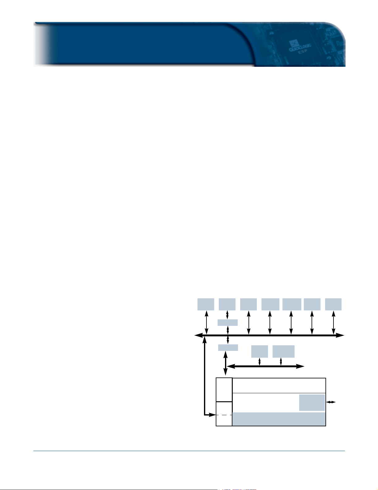
CPU
• High-performance MIPS 4Kc processor runs
up to 133 MHz in .25µ
(173 Dhrystone MIPS)
• 1.3 Dhrystone MIPS per MHz
• MDU supports MAC instructions for
DSP functions
• 16 Kbytes of Instruction Cache
(4-way set associative)
• 16 Kbytes of Data Cache (4-way set
associative) with lockout capability per line
• 16 Kbytes of on-chip, high-speed SRAM for
use by multiple AHB Bus Masters
• 32-bit 66/33 MHz PCI Host and Satellite
(Master/Target) operation with DMA
channels and FIFO for full bandwidth
• Two MAC10/100s with MII ports connect
easily to external transceivers/PHY devices
• One AHB 32-bit master port/one AHB
32-bit slave port to Programmable Fabric
• Global System Configuration and Interrupt
Controller
Peripheral Bus (AMBA APB)
• 32-bit APB runs at half the CPU clock
frequency (the same as the AHB clock)
• Three APB slave ports in the programmable
fabric
• Two serial ports (one with Modem control
signals and one with IRDA-compliant signals)
• Four general-purpose 32-bit timer/counters
on one APB port
16 Kbytes
SRAM
MIPS 4Kc
w/Caches
32-bit PCI
66/33 MHz
Ethernet
10/100 MAC
Ethernet
10/100 MAC
Memory
Controller
Interrupt
Controller
High-Perf ormance Bus (AMBA AHB)
• High-performance 32-bit AMBA AHB bus
standard for high-speed system bus running
at half the CPU clock
• High-bandwidth memory controller for
SDRAM, SRAM, and EPROM
• SDRAM support for standard SDRAMs up to
256 MBytes with auto refresh, up to 4 banks
non-interleaved
• Support for PC100 type memories with up
to two chip enables
• EPROM controller for boot code
• 8-bit, 16-bit, and 32-bit device width support
QL901M QuickMIPSTM Data Sheet Rev B
ECI to AHB
32-bit Advanced High-Performance Bus
AHB to APB
3 APB
Slave
I/F
1 AHB
Master I/F
1 AHB
Slave I/F
Two 16550
UARTs
32-bit Advanced Peripheral Bus
36 RAM Blocks (Configurations 128x18; 256x9; 512x4; or 1024x2)
Via-Link Programmable Fabric
18 ECU Blocks-- 8x8 Multiply, 16-bit carry/add
Four 32-bit
Timer/Counters
Configurable
Logic Analyzer
Monitor (CLAM)
Figure 1: Embedded QuickMIPS Block Diagram
JTAG
•
•
1
•
•
•
•

Programmable Via-Link Fabric
• Embedded memory configurable as RAM or FIFO
• 252 programmable I/Os
• High-speed dynamically configurable ECUs enable hardware implementation of DSP functions with
3-bit instructions
• Fabric I/O standard options: LVTLL, LVCMOS, PCI, GTL+, SSTL, and SSTL3
Table 1: Programmable Fabric F eatures
Maximum System Gates*
536,472 72x28 2,016 4,788 36 82,944 18
* 75K ASIC gates
Logic Arrays
Columns x Rows
Logic Cells
** Possible Configurations:
128x18, 256x9, 512x4, or 1024x2
Maximum
Flip-Flops
RAM Blocks** RAM Bits ECU Blocks***
*** 8x8 Multiply ,
16-bit carry-add
On-Chip Debug Blocks
• On-chip instrumentation blocks for debug and trace capabilities
• Configurable Logic Analysis Module (CLAM) blocks with IP in programmable fabric allow user to look
at selected signals from IP function in fabric
Development and Programming
• Complete QuickLogic software suite of development tools enables rapid implementation of IP
functions for complete SOC solution
• Complete chip simulation of user-defined programmable-logic IP functions with the processor,
caches, memory, and all hardwired functions on-chip
• Synthesis of IP functions into the programmable fabric
• Place-and-Route tool for efficient implementation of IP functions in the programmable fabric
• Extensive timing analysis of IP functions with the rest of the chip to ensure full chip functionality
• Programming and debug support of the entire chip through JTAG port
• Integrated debug support for the MIPS 4Kc processor
• MIPS Language and Debug tool support for the MIPS 4Kc processor from approved third party
MIPS vendors
• ECU support for a variety of DSP algorithms and functions
• QuickLogic library of standard IP functions for plug-and-play implementation of standard IP functions
in the programmable fabric for a complete SOC solution
• QuickMIPS Reference Design Kit (RDK) provides a complete Board Support Package for
chip evaluation
• Programming and debug support
• Device-driver support for standard IP functions
• Boot-up code and diagnostics
•
•
2
www.quicklogic.com
•
•
•
•
© 2001 QuickLogic Corporation
Design Tools Platform Support
• QuickWorks, the complete product suite, supports Windows 95/98/NT/2000. It includes SpDE
(layout including place & route, timing analysis, and back-annotation), Synplify-Lite (synthesis), Turbo
Writer (HDL-enhanced text editor), etc.
• QuickTool supports Solaris. It has only the layout software (SpDE).
• QuickMIPS simulation is enabled through either:
• a SmartModel (VMC-generated model, encrypted RTL, relatively slow). This option supports both
Verilog and VHDL.
• SaiLAhead co-verification platform from Saivision (very fast C model). This option only supports
Verilog (no VHDL) at this time.
Table 2: Design Tools Platform Support
Solaris Windows NT Windows 2000 Linux
Synthesis Synplify-Lite X (in QuickWorks) X (in Qui ckW orks)
Layout SpDE X (in QuickTool) X (in QuickWorks) X (in QuickWorks)
SmartModel
Simulation
SaiLAhead
ModelSim/VCS XX
Verilog XL/NC X
ModelSim XXX
Verilog XL/NC X X
SaiLAhead Platform
The “SaiLAhead for QuickMIPS” co-verification platform is tailored for QuickMIPS devices. It enables
simulation of user-defined logic functions that are to be implemented in the QuickMIPS programmable
fabric with the rest of the QuickMIPS fixed system logic functions, which verifies overall QuickMIPS
functionality. Simultaneously, the SaiLAhead platform has a powerful, feature-rich debugger, which
enables QuickMIPS users to develop and debug their application code (C and MIPS assembly). The
SaiLAhead platform accelerates the speed of simulation of the QuickMIPS device in a simulator such as
NC-Verilog by using C models for various fixed system logic functions in the QuickMIPS device. This
platform also provides a standalone C environment offering additional speed-up of simulation of the
entire QuickMIPS design. Please refer to
SaiLAhead platform.
http://www.saivision.com for more information on the
QL901M QuickMIPS™ Data Sheet Rev B
•
3
•
•
•
•
•
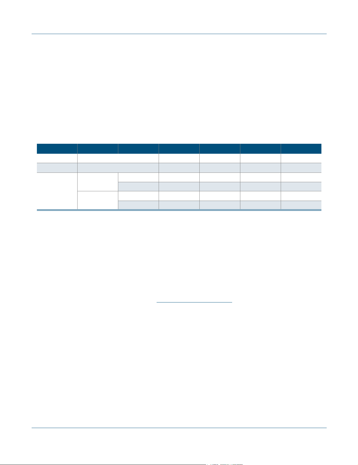
2.0 Embedded Computational Units (ECUs)
Traditional programmable logic architectures do not implement arithmetic functions efficiently or
effectively. These functions require high logic cell usage while garnering only moderate performance
results. By embedding a dynamically reconfigurable computational unit, the QuickMIPS chip can address
various arithmetic functions efficiently and effectively providing for a robust DSP platform. This
approach offers greater performance than traditional programmable logic implementations. The ECU
block is ideal for complex DSP, filtering, and algorithmic functions. The QuickMIPS architecture allows
functionality above and beyond that achievable using DSP processors or programmable logic devices.
The embedded block is implemented at the transistor level with the following block diagram in
Figure 2.
Abus
Xbus
Ybus
I bus
Sign
Multiply
Sequencer
Add Register
Logic CellMemory
16
8
8
3
2
1
17
Rbus
Figure 2: Embedded Computational Unit (ECU) Block Diagram
Table 3: ECU Comparisons
Function Description
16 bit 8 ns 2.5 ns
Adder
Multiplier
System Clock 200 MHz 400 MHz
32 bit 10 ns 5.6 ns
64 bit 12 ns 6.7 ns
8 x 8 10 ns 4.3 ns
16 x 16 12ns 6.7 ns
Slowest Speed
Grade
Fastest Speed Grade
Implementation of the equivalent ECU block as HDL in a programmable logic architecture requires 205
logic cells with a 10 ns delay in a -4 speed grade. There are a maximum of 18 ECU blocks and a
minimum of 10 ECU blocks in the QuickMIPS chip. The ECU blocks are placed next to the RAM
circuitry for efficient memory/instruction fetch and addressing for DSP algorithmic implementations.
Eighteen 8-bit Multiply Accumulate functions can be implemented per cycle for a total of 2.6 billion
MACs/s when clocked at 144 MHz. Further Multiply Accumulate functions also can be implemented in
the programmable logic.
•
•
4
www.quicklogic.com
•
•
•
•
© 2001 QuickLogic Corporation
The ECU block can be configured for eight arithmetic functions via an instruction as shown in Table 4.
The modes for the ECU block are dynamically reprogrammable through the Instruction Set Sequencer.
Table 4: ECU Mode Select Criteria
Instruction Set Operation
0 0 0 Multiply
0 0 1 Multiply - Add
010 Accumulate
0 1 1 Add
1 0 0 Multiply (registered)
1 0 1 Multiply - Add (registered)
1 1 0 Multiple - Accumulate
1 1 1 Add (registered)
The Sequencer can be a variety of logic operators, such as a FIFO loaded with various algorithms, an
external software driven algorithm, or an internal state machine. This flexibility allows the designer to
reconfigure the ECU for algorithmic intensive applications in which functions change on the next clock
cycle, such as adaptive filtering.
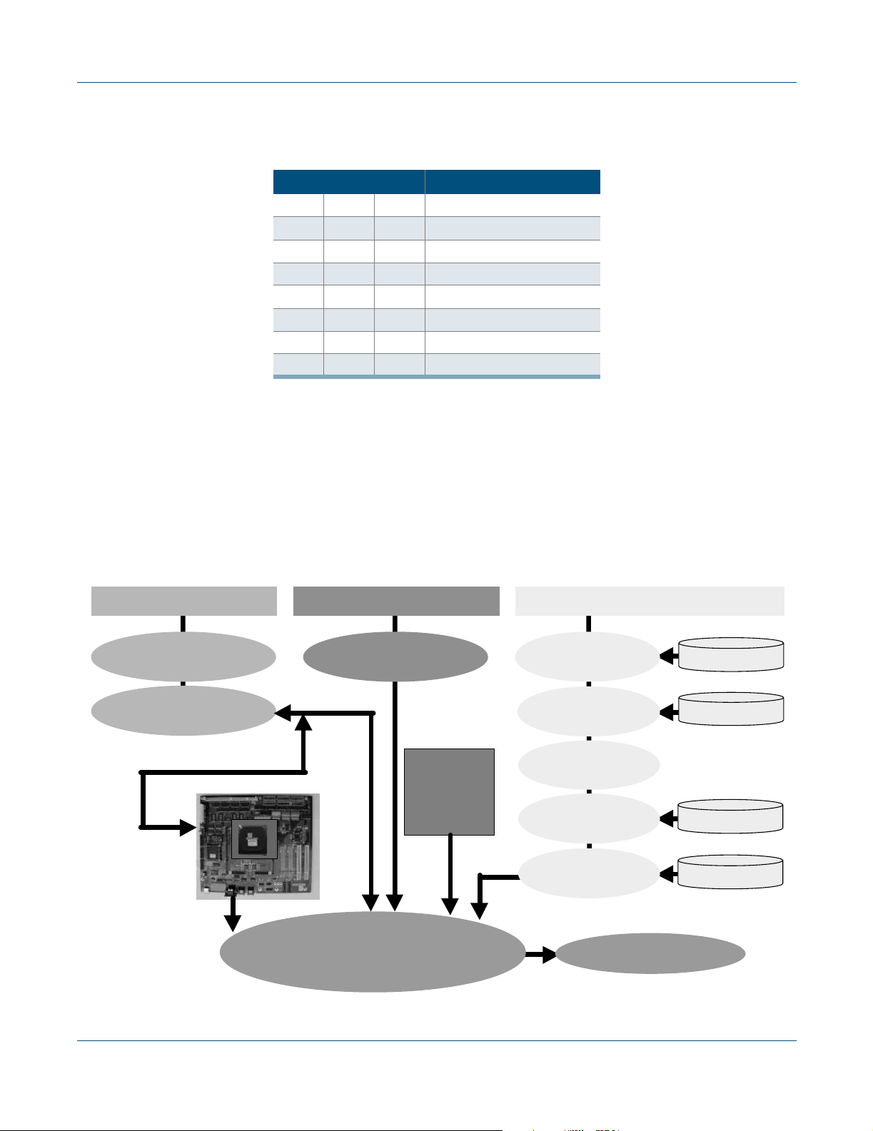
3.0 Design Flow
The QuickMIPS design flow, similar to ASIC design flow, is shown in Figure 3.
MIPS Programming System Configuration Customer IP Design in FPGA
Compiler,
Assembler, Linker
Debugger
EJTAG
Board-level
Support Package
Functional Co-simulation
Global Register
Configuration
QuickMIPS
System
Model
Full-System
with Timing
RTL
Synthesis
Place & Route
Timing Analysis
Final Netlist
& Timing
Chip Programming
QuickIP Models
Synthesis Lib
Timing Lib
QuickIP Netlist
Figure 3: QuickMIPS Hardware/Software Co-Development Flow
QL901M QuickMIPS™ Data Sheet Rev B
•
5
•
•
•
•
•

A typical design process goes through the flow shown above. After passing postlayout simulation,
QuickMIPS devices can be programmed for testing on the hardware testbench. Because QuickLogic
devices are One-Time-Programmable (OTP), it is recommended that these devices are programmed only
after they pass postlayout simulation to minimize development cost and reduce bench debugging time.
The QuickMIPS design flow is supported by QuickLogic's QuickWorks™ (for Microsoft Windows) and
QuickTool™ (for UNIX) design software suites version 9.2 and up. Many third-party synthesis and
simulation tools are also supported. The QuickWorks software suite can be downloaded from
QuickLogic's Web site
(www.quicklogic.com). Please contact a QuickLogic sales representative to
obtain a license or get QuickTool software.
Both Verilog and VHDL design methodologies are fully supported. The flow described below assumes
that the QuickWorks or QuickTool 9.2 software has been installed.
3.1 Simulation
QuickLogic provides the system simulation environment. This environment includes the QuickMIPS
VMC model, ROM and RAM models, reset and clock generation, boot code, and sample programs (read
and write to memory). This environment allows customers to focus on their RTL code and not have to
worry about bringing up the system simulation environment.
The simulation behavior of the QuickMIPS ESP core is provided by the VMC model. VMC (Verilog
Model Compiler) is a tool from Synopsys that compiles Verilog RTL (Register-Transfer-Level) code into
binary code. A VMC model (the binary code) implements the same logic functions as the RTL code while
providing IP protection. In simulation, it communicates to the simulator via PLI (Programmable
Language Interface) for Verilog or FLI (Foreign Language Interface) for VHDL.
Because of the VMC model, the Silos III Verilog simulator and Active-HDL VHDL simulator bundled in
QuickWorks are not supported in QuickMIPS simulation flow. A third-party simulator must be used. The
currently supported simulators include:
• Verilog simulators: Verilog-XL, NC Verilog, VCS, ModelSim
• VHDL simulators: VSS, ModelSim
3.2 Synthesis
Synthesis is the process of turning the HDL code describing the fabric behavior into gates. Three thirdparty synthesis tools are supported:
• Synplify-Lite from Synplicity (bundled in QuickWorks)
• Exemplar Leonardo Spectrum
• Synopsys Design Compiler
Refer to the corresponding QuickNotes on the QuickLogic support Web site for further information.
•
•
6
www.quicklogic.com
•
•
•
•
© 2001 QuickLogic Corporation

3.3 Layout
Layout is performed in SpDE, which is the QuickLogic layout environment in both QuickWorks and
QuickTool. The input to the layout is a netlist from synthesis. SpDE can accept netlists in both the
QuickLogic format
(.qdf) and industry standard EDIF.
3.4 Programming
Once it has been determined that the design is functionally correct and meets the desired timing
constraints, run the sequencer and save the <design>.chp file. You can either import the design into
QuickPro if you want to program it yourself, or submit the file to QuickLogic's WebASIC service to obtain
programmed devices overnight at the following URL:
QuickPro is the software to program a .chp file into QuickLogic devices. It is freeware and does not
require a license. You can download it from the QuickLogic Web site. It runs only on Microsoft Windowsbased PCs. To program your device, you also need a programmer called DeskFab and a programming
adapter for the package you are using. Please contact a QuickLogic sales representative when you are
handling the programming.
www.quicklogic.com/webasic.
QL901M QuickMIPS™ Data Sheet Rev B
•
7
•
•
•
•
•
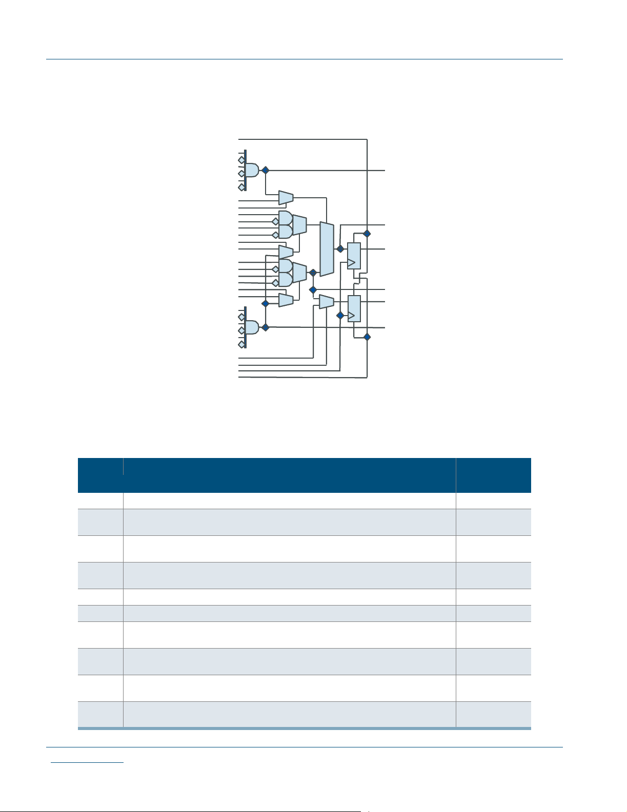
4.0 AC Characteristics at Vcc = 2.5V, TA=25° C (K=0.74)
The AC Specifications, Logic Cell diagrams, and waveforms are provided below.
Figure 4: QuickMIPS Logic Cell
Table 5: Logic Cells
Symbol Parameter
Logic Cells
tPD Combinatorial delay: time taken by the combinatorial circuit to output 0.257
tSU
tCLK
tCWHI Clock High Time: the length of time that the clock stays high 0.46
tCWLO Clock Low Time: the length of time that the clock stays low 0.46
tSET
tRESET
tSW
tRW
Setup time: the amount of time the synchronous input of the flip flop must be stable before
the active clock edge
Hold time: the amount of time the synchronous input of the flip flop must be stable after the
thl
active clock edge
Clock to out delay: the amount of time the synchronous input of the flip flop must be stable
after the active clock edge
Set Delay: amount of time between when the flip flop is “set” (high)
and when Q is consequent “set” (high)
Reset Delay: amount of time between when the flip flop is “reset” (low) and when Q is
consequent “reset” (low)
Set Width: length of time that the SET signal remains high
(low if active low)
Reset Width: length of time that the RESET signal remains high
(low if active low)
Propagation
delay (ns)
0.22
0
0.255
0.18
0.09
0.3
0.3
•
•
8
www.quicklogic.com
•
•
•
•
© 2001 QuickLogic Corporation
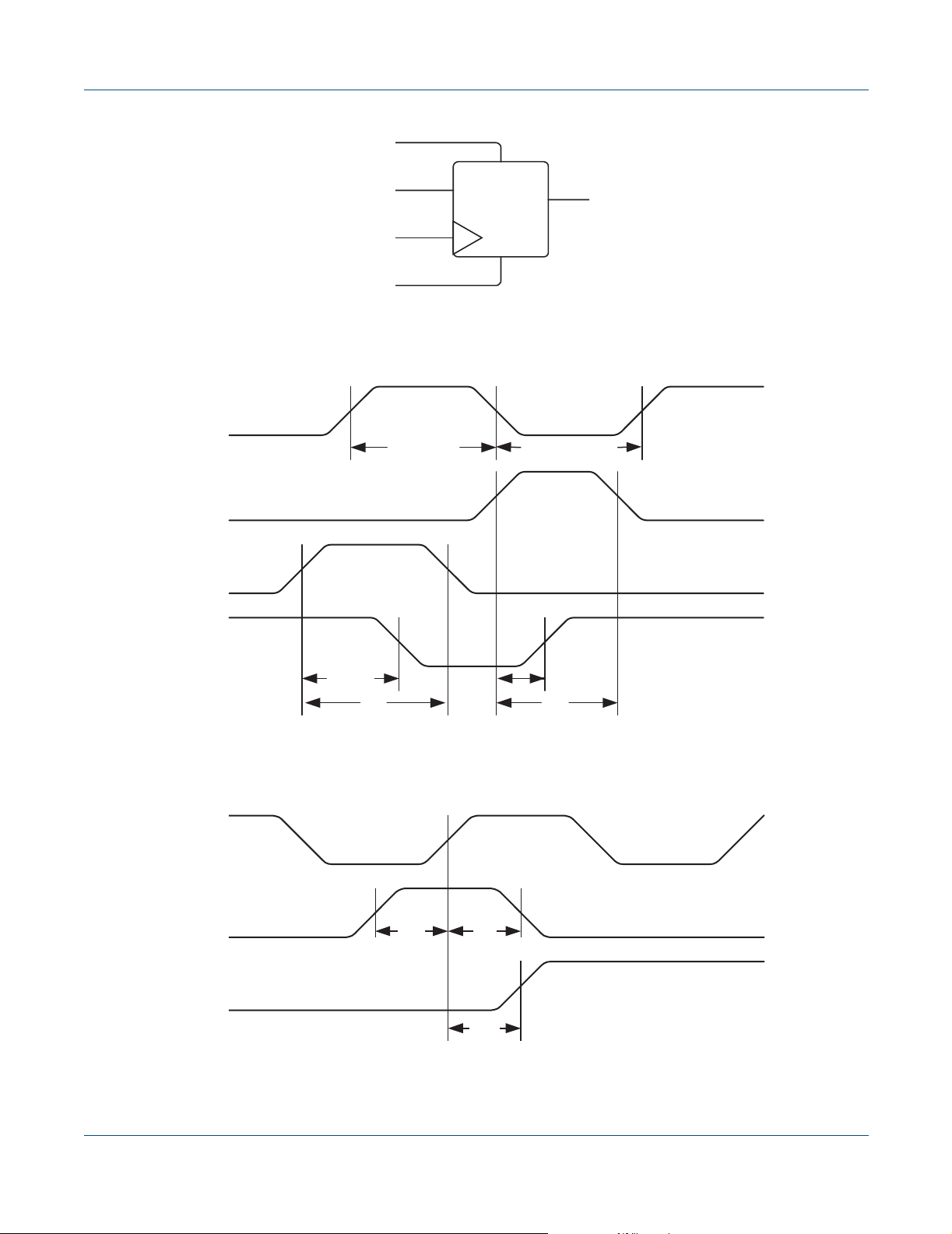
SET
CLK
SET
RESET
Q
D
CLK
RESET
Figure 5: Logic Cell Flip Flop
tCWI (min)
Q
tCWLO (min)
CLK
D
Q
tRESET
tRW
tSET
tSW
Figure 6: Logic Cell Flip Flop Timings - First Waveform
tSU
tHL
tCLK
Figure 7: Logic Cell Flip Flop Timings - Second Waveform
QL901M QuickMIPS™ Data Sheet Rev B
•
9
•
•
•
•
•
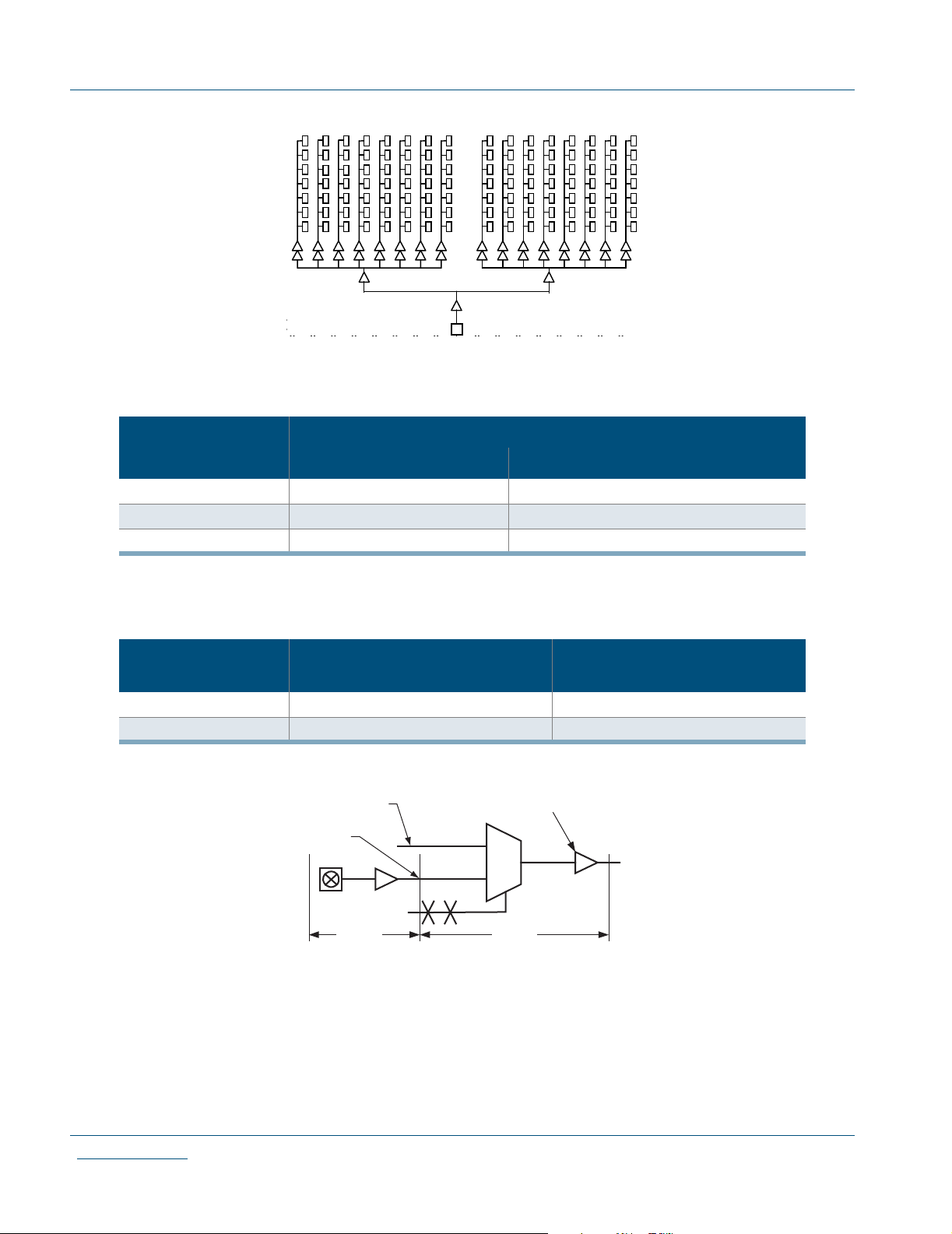
Figure 8: QuickMIPS Global Clock Structure
Table 6: QuickMIPS Clock Performance
Clock Performance
Global Dedicated
Macro
I/O
Skew
Symbol
Input Register Cell Only
tGCKP Global clock pin delay to quad net 1.34
GCKB Global clock buffer delay (quad net to flip flop) 0.56
Programmable Clock
Hardware Clock
1.51 ns 1.59 ns
2.06 ns 1.73 ns
0.55 ns 0.14 ns
Table 7: QuickMIPS Input Register Cell
Parameter Propagation delay (ns)
Global Clock Buffer
Global Clock
tPGCK tBGCK
10
•
•
www.quicklogic.com
•
•
•
•
Figure 9: Global Clock Structure Schematic
© 2001 QuickLogic Corporation
[9:0]
WA
RE
[17:0]
WD
WE
WCLK
[1:0]
MODE ASYNCRD
Quick RAM Mod ule
Figure 10: RAM Module
Table 8: RAM Cell Synchronous Write Timing
Symbol Parameter
RAM Cell Synchronous Write Timing
tSWA
tHWA
tSWD
tHWD
tSWE
tHWE
tWCRD
WA setup time to WCLK: the amount of time the WRITE ADDRESS must be
stable before the active edge of the WRITE CLOCK
WA hold time to WCLK: the amount of time the WRITE ADDRESS must be
stable after the active edge of the WRITE CLOCK
WD setup time to WCLK: the amount of time the WRITE DATA must be stable
before the active edge of the WRITE CLOCK
WD hold time to WCLK: the amount of time the WRITE DATA must be stable
after the active edge of the WRITE CLOCK
WE setup time to WCLK: the amount of time the WRITE ENABLE must be
stable before the active edge of the WRITE CLOCK
WE hold time to WCLK: the amount of time the WRITE ENABLE must be stable
after the active edge of the WRITE CLOCK
WCLK to RD (WA=RA): the amount of time between the activ e WRITE CLOCK
edge and the time when the data is available at RD
RCLK
RA
RD
[9:0]
[17:0]
Propagation
delay (ns)
0.675
0
0.654
0
0.623
0
4.38
QL901M QuickMIPS™ Data Sheet Rev B
•
11
•
•
•
•
•
WCLK
WA
tSWA
WD
tSWD
WE
tSWE
RD
old data
Figure 11: RAM Cell Synchronous Write Timing
Table 9: RAM Cell Synchronous & Asynchronous Read Timing
Symbol Parameter
RAM Cell Synchronous Read Timing
tSRA
tHRA
tSRE
tHRE
tRCRD
RAM Cell Asynchronous Read Timing
rPDRD
RA setup time to RCLK: the amount of time the READ ADDRESS must
be stable before the active edge of the READ CLOCK
RA hold time to RCLK: the amount of time the READ ADDRESS must
be stable after the active edge of the READ CLOCK
RE setup time to WCLK: the amount of time the READ ENABLE must be
stable before the active edge of the READ CLOCK
RE hold time to WCLK: the amount of time the READ ENABLE must be
stable after the active edge of the READ CLOCK
RCLK to RD: the amount of time between the active READ CLOCK edge
and the time when the data is available at RD
RA to RD: amount of time between when the READ ADDRESS is input
and when the DATA is output
tHWA
tHWD
tHWE
new data
tWCRD
Propagation
delay (ns)
0.686
0
0.243
0
4.38
2.06
12
•
•
www.quicklogic.com
•
•
•
•
© 2001 QuickLogic Corporation

RCLK
RA
RE
tSRA tHRA
RD
tSRE
old data
rPDRD
tHRE
new data
tRCRD
Figure 12: RAM Cell Synchronous & Asynchronous Read Timing
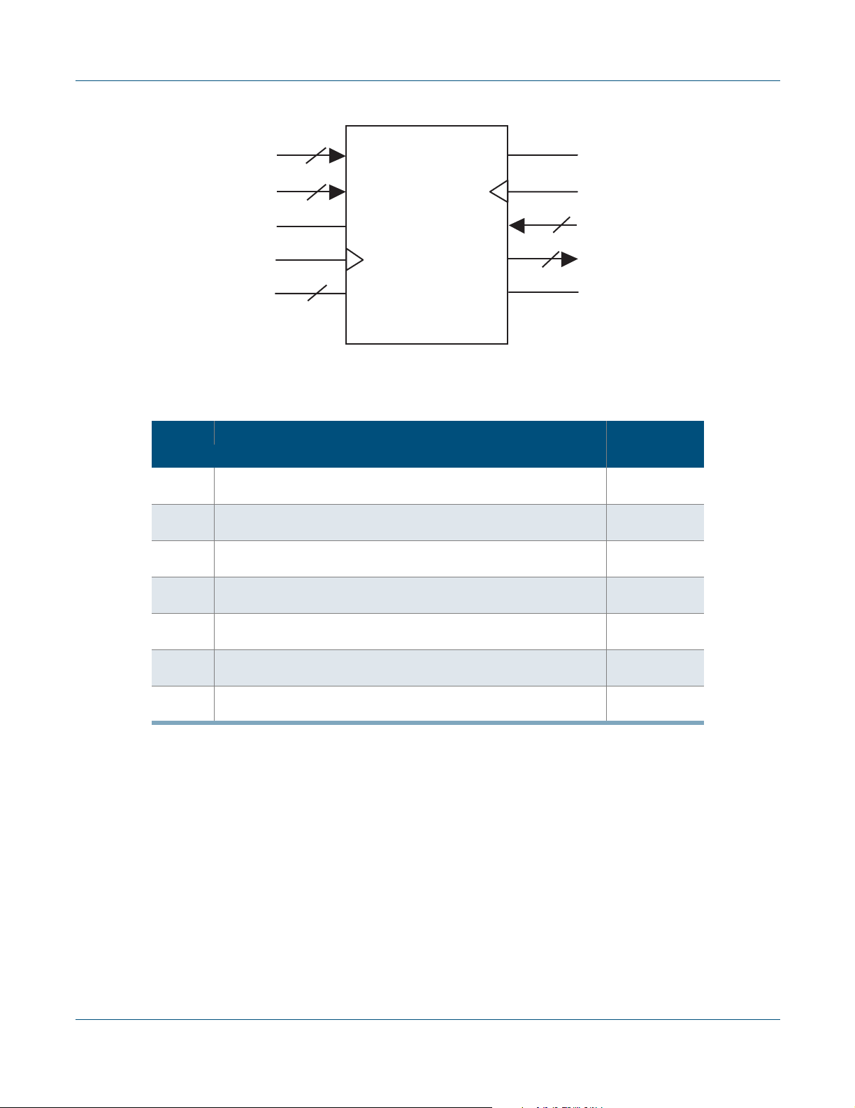
+
-
INPUT
REGISTER
OUTPUT
REGISTER
Q
E
D
R
Q
D
R
PAD
OUTPUT ENABLE
QL901M QuickMIPS™ Data Sheet Rev B
E
Q
REGISTER
D
R
Figure 13: QuickMIPS Cell I/O
•
13
•
•
•
•
•

tIN, tINI
tICLK
tISU
+
-
Q
E
D
R
tSID
PAD
Figure 14: QuickMIPS Input Register Cell
Table 10: Input Register Cell
Symbol Parameter
Input Register Cell Only
tISU
tIH
tICLK
tIRST
tIESU
tIEH
Input register setup time: the amount of time the synchronous input of
the flip flop must be stable before the active clock edge
Input register hold time: the amount of time the synchronous input of the
flip flop must be stable after the active clock edge
Input register clock to Q: the amount of time taken by the flip flop to
output after the active clock edge
Input register reset delay: amount of time between when the flip flop is
“reset”(low) and when Q is consequently “reset” (low)
Input register clock enable setup time: the amount of time “enable” must
be stable before the active clock edge
Input register clock enable time: the amount of time “enable” must be
stable after the active clock edge
Propagation
delay (ns)
3.12
0
1.08
0.99
0.37
0
14
•
•
www.quicklogic.com
•
•
•
•
© 2001 QuickLogic Corporation

Table 11: Standard Input Delays
Symbol Parameter
Propagation
Standard
Input Delays
tSID (LVTTL) LVTTL input delay: Low Voltage TTL for 3.3V applications 0.34
tSID (LVCMOS2)
tSID (GTL+) GTL+ input delay: Gunning Transceiver Logic 0.68
tSID (SSTL3) SSTL3 input delay: Stub Series Terminated Logic for 3.3V 0.55
tSID (SSTL2) SSTL2 input delay: Stub Series Terminated Logic for 2.5V 0.607
To get the total input delay and this delay to tISU
LVCMOS2 input delay: Low Voltage CMOS for 2.5V and lower
applications
delay (ns)
R
CLK
0.42
D
tISU
Q
tIHL
tICLK
tIRST
E
tIESU
tIEH
Figure 15: QuickMIPS Input Register Cell Timing
QL901M QuickMIPS™ Data Sheet Rev B
•
15
•
•
•
•
•

PAD
OUTPUT
REGISTER
Figure 16: QuickMIPS Output Register Cell
Table 12: QuickMIPS Output Register Cell
Symbol Parameter
Output Register Cell Only
tOUTLH Output Delay low to high (10% of H)
tOUTHL Output Delay high to low (90% of H)
tPZH Output Delay 3-state to high (10% of Z)
tPZL Output Delay 3-state to low (90% of Z)
tPHZ Output Delay high to 3-state
tPLZ Output Delay low to 3-state
tCO Clock to out delay
Propagation
delay (ns)
0.40
0.55
2.94
2.34
3.07
2.53
3.15 (fast slew)
10.2(slow slew)
16
•
•
www.quicklogic.com
•
•
•
•
© 2001 QuickLogic Corporation

H
H
tOUTHL
Rising Edge
Falling Edge
L
tOUTLH
H
Z
L
tPZH
H
Z
L
tPLZ
L
H
Z
L
H
Z
L
tPZL
tPHZ
Figure 17: QuickMIPS Output Register Cell Timing
Table 13: VCCIO = 3.3 V
Fast Slew Slow Slew
2.8 V/ns 1.0 V/ns
2.86 V/ns 1.0 V/ns
Table 14: VCCIO = 2.5 V
Fast Slew Slow Slew
Rising Edge
Falling Edge
Jitter
<200ps 157
Standby
Current (
1.7 V/ns 0.6 V/ns
1.9 V/ns 0.6 V/ns
Table 15: ESP PLL Timing Parameters
Frequency Range
µ
a)
µ
a 40-66.6 MHz 25 MHz 60/40 200 PPM 10
Minimum Lock
Frequency
Duty
Cycle
Crystal
Accuracy
Lock Time
µ
s
QL901M QuickMIPS™ Data Sheet Rev B
•
17
•
•
•
•
•

PCI_AD(output)[31:0]
PCI_C_BE_n(output)[3:0]
PCI_PAR(output)
PCI_FRAME_n(output)
PCI_IRDY_n(output)
PCI_TRDY_n(output)
PCI_STOP_n(output)
PCI_DEVSEL_n(output)
PCI_SERR_n
PCI_PERR_n(output)
PCI_AD(input)[31:0]
PCI_C_BE_n(input)[3:0]
PCI_PAR(input)
PCI_FRAME_n(input)
PCI_IRDY_n(input)
PCI_TRDY_n(input)
PCI_STOP_n(input)
PCI_DEVSEL_n(input)
PCI_PERR_n(input)
PCI_LOCK_n
PCI_CLK
Tval
Tval(ptp)
PCI_REQ_n
Tsu Th
PCI_IDSEL
18
•
•
www.quicklogic.com
•
•
•
•
Tsu(ptp)
PCI_GNT_n
Figure 18: PCI Waveforms
© 2001 QuickLogic Corporation

Table 16: P CI AC Timing
Parameter
a
66 MHz 33 MHz
Min Max Min Max
Tcyc PCI_CLK Cycle Time 15 30 ns
Thigh PCI_CLK High Time 6 11 ns
Tlow PCI_CLK Low Time 6 11 ns
– PCI_CLK Slew Rate 1.5 4 1 4 V/ns
Tval PCI_CLK to Signal Valid Delay 2 6 2 11 ns
Tval (ptp)
Ton Float to Active Delay 2 2 ns
Toff Active to Float Delay 14 28 ns
Tsu
Tsu (ptp)
Th Input Hold Time from PCI_CLK 0 0 ns
Trst Reset Active Time after power stable 1 1 ms
Trst-clk Reset Active Time after PCI_CLK stable 100 100
Trst-off
Trhfa PCI_RST_n high to first configuration access 2 2 clocks
Trhff PCI_RST_n high to first PCI_FRAME_n assertion 5 5 clocks
PCI_CLK to Signal Valid Delay
point-to-point signals
Input Setup Time to PCI_CLK
bused signals
Input Setup Time to PCI_CLK
point-to-point
c
Reset Active to output float delay 40 40 ns
b
2 6 2 12 ns
37ns
5 10, 12 ns
Units
µ
s
a. All PCI pins are synchronous to the PCI clock except for PCI_RST_n and PCI_INTA_n.
b. Point-to-point signals include PCI_REQ_n and PCI_GNT_n.
c. All output drivers must be 3-stated when PCI_RST_n is active.
TXCLK(in)
TXEN(out)
t
en_c2q
TXD[3:0](out)
t
en_c2q
t
data_v
t
data_h
t
data_h
Figure 19: Ethernet MAC Transmit Interface Waveforms
Table 17: Ethernet MAC Transmit Interface AC Timing
Parameter Min Max Units
Time from the rising clock edge of TXCLK to
the change in TXEN
Time from the rising clock edge of TXCLK to all
data signals having valid stable values
Time in which the output data is still valid after
the rising clock edge of TXCLK
t
data_v
0.0 ns
8.0 ns
9.0 ns
QL901M QuickMIPS™ Data Sheet Rev B
•
19
•
•
•
•
•

RXCLK(in)
RXDV(in)
t
dv_h
t
dv_s
RXER(in)
t
er_h
t
er_s
RXD[3:0](in)
t
data_s
Figure 20: Ethernet MAC Receive Interface Waveforms
Table 18: Ethernet MAC Receive Interf a c e AC Timing
Parameter Min Max Units
t
dv_s
t
dv_h
t
er_s
t
er_h
t
data_s
t
data_h
RXDV (receive data valid) to RXCLK setup time 2.0 ns
RXDV (receive data valid) from RXCLK hold time 2.0 ns
RXER (receive data error) to RXCLK setup time 2.0 ns
RXER (receive data error) from RXCLK hold time 2.0 ns
RXD (receive data) to RXCLK setup time 2.0 ns
RXD (receive data) from RXCLK hold time 2.0 ns
The timing of the MII Management Interface listed below depends on the system clock frequency. The
numbers displayed are correct for a processor clock frequency of 100 MHz and an AMBA bus system
clock frequency of 50 MHz. Note that for a system clock of 133 MHz, the mandatory MDC minimum
clock cycle of 400ns for some PHY devices will not be met.
t
data_h
20
•
•
www.quicklogic.com
•
•
•
•
© 2001 QuickLogic Corporation

t
mdc_cyc
t
mdc_h
t
mdc_l
t
mdozv
t
mdovz
t
mdos
t
mdovh
t
mdc_cyc
t
t
mdc_h
mdc_l
MDC(out)
MDIO(out)
t
mdozv
t
mdovh
t
mdovs
Figure 21: MII Management Interface Waveforms (1 of 2)
Table 19: MII Management Interface AC Timing (1 of 2)
Parameter Min Max Units
MDC cycle time 520 ns
MDC high time 260 ns
MDC low time 260 ns
MDIO output high impedance to valid time from rising edge of MDC 40 ns
MDIO output valid to high impedance time from rising edge of MDC 40 ns
MDIO output valid before MDC rising edge 440 ns
MDIO output valid from MDC rising edge 40 ns
t
mdovz
t
t
mdis
mdih
MDC(out)
MDIO(in)
t
mdis
Figure 22: MII Management Interface Waveforms (2 of 2)
Table 20: MII Management Interface AC Timing (2 of 2)
Parameter Min Max Units
MDIO setup time to MDC 25 ns
MDIO hold time to MDC 0 ns
t
mdih
QL901M QuickMIPS™ Data Sheet Rev B
•
21
•
•
•
•
•

SD_CS_n[3:0]
SD_CKE[3:0]
SD_DQM[3:0]
DATA(output)[31:0]
DATA(input[31:0]
SD_CLKIN
Tco_sdram
ADDR[23:0]
SD_RAS_n
SD_CAS_n
SD_WE_n
Tsu_sdram Th_sdram
Figure 23: SDRAM Waveforms
Table 21: SDRAM AC Timing
Parameter
Tco
Tsu DATA 12 ns
Th DATA 2 ns
a. All timing is measured with respect to the rising edge of SD_CLKIN. All measurements are based on I/Os with 35 pF
load except for SD_CLKOUT, which has a load of 15 pF.
DATA, ADDR, SD_RAS_n, SD_CAS_n, SD_CS_n[3:0],
SD_DQM[3:0], SD_WE_n, SD_CKE[3:0]
a
Min Max Units
28ns
Internal_AHB_Clock
CS_n
ADDR[31:0]
BLS_n[3:0]
addraddr
byte lane selectbyte lane select
OEN_n
WEN_n
D0
D1
DATA[31:0]
read dataread data
22
•
•
www.quicklogic.com
•
•
•
•
Figure 24: SRAM Read Waveforms
© 2001 QuickLogic Corporation

Internal_AHB_Clock
CS_n
ADDR[31:0]
BLS_n[3:0]
OEN_n
WEN_n
DATA[31:0]
addraddr
byte lane selectbyte lane select
D0
D1
write datawrite data
Figure 25: SRAM Write Waveforms
Table 22
and Table 23 below list the synchronous and asynchronous timing for the QuickMIPS Fabric
interface port. Note the following with regards to the fabric timing:
1 fb_int is asynchronous and is synchronized inside the core.
2 fb_bigendian is a static signal and reflects the value on the CPU_BIGENDIAN pin.
3 pm_* and si_* signals are synchronous to the internal MIPS clock which is twice the hclk frequency. Because this internal
clock is not brought to the outside, these signals are considered asynchronous.
4 All AF_PCI_* signals are static.
Table 22: QuickMIPS Interface Port Synchronous Timing (to hclk)
Setup Time (Tsu) Hold Time (Thold) Clock-to-out Time (Tco)
hresetn x
Fabric AHB Slave Ports
ahbs_hsel X X 10.73
ahbs_haddr X X 10.56
ahbs_htrans X X 11.35
ahbs_hwrite X X 8.32
ahbs_hsize X X 9.50
ahbs_hburst X X 9.12
ahbs_hprot X X 9.66
ahbs_hwdata X X 13.07
ahbs_hrdata 5.94 0 X
ahbs_hready_out 9.55 0 X
ahbs_hresp 10.39 0 X
Fabric AHB Master Ports
ahbm_haddr 11.94 0 X
ahbm_htrans 11.33 0 X
ahbm_hwrite 10.39 0 X
ahbm_hsize 10.58 0 X
a
x5.11
(Sheet 1 of 2)
QL901M QuickMIPS™ Data Sheet Rev B
•
23
•
•
•
•
•

Table 22: QuickMIPS Interface Port Synchronous Timing (to hclk) (Continued)
Setup Time (Tsu) Hold Time (Thold) Clock-to-out Time (Tco)
ahbm_hburst 10.79 0 X
ahbm_hprot
ahbm_hwdata 10.39 0 X
ahbm_hrdata X X 16.28
ahb_hready_in X X 11.82
ahbm_hresp X X 9.02
ahbm_hbusreq 7.40 0 X
ahbm_hgrant X X 16.64
Fabric APB Slave Ports
apbs_paddr X X 4.52
apbs_pwdata X X 4.66
apbs_penable X X 2.87
apbs_pwrite X X 4.13
apbs_psel0 X X 3.80
apbs_psel1 X X 3.43
apbs_psel2 X X 3.25
apbs_prdata0 7.44 0 X
apbs_prdata1 6.79 0 X
apbs_prdata2 6.97 0 X
Timer Ports
tm_fbenable 0.23 0 X
tm_overflow2 X X 4.35
tm_overflow3 X X 4.48
tm_overflow4 X X 5.00
b
– – X
(Sheet 2 of 2)
24
a. “x” indicates that this timing delay does not apply to the signal.
b. The ahbm_hprot
ters besides the processor-AHB-bridge generates this signal. Therefore the re is no setup or hold timing for
ahbm_hprot.
•
•
www.quicklogic.com
•
•
•
•
signal is NOT used by any slave within the standard cell part of the chip. None of the mas-
© 2001 QuickLogic Corporation

Table 23: QuickMIPS Interface Port Asynchronous Timing
Start Port End Port Propagation Delay (Tprop)
ahbm_haddr ahbs_haddr 8.39
ahbm_haddr ahbs_hsel 7.71
ahbm_htrans ahbs_htrans 6.48
ahbm_hwrite ahbs_hwrite 6.21
ahbm_hsize ahbs_hsize 6.04
ahbm_hburst ahbs_hburst 5.70
ahbm_hprot ahbs_hprot 7.07
ahbm_hwdata ahbs_hwdata 8.15
ahbs_hrdata ahbm_hrdata 5.78
ahbs_hready_out ahb_hready_in 5.03
ahbs_hresp ahbm_hresp 4.98
ahbm_hbusreq ahbm_hgrant 10.14
ahbs_hresp ahbm_hgrant 10.50
apbs_prdata0 ahbm_hrdata 8.28
apbs_prdata1 ahbm_hrdata 7.51
apbs_prdata2 ahbm_hrdata 7.57
QL901M QuickMIPS™ Data Sheet Rev B
•
25
•
•
•
•
•

5.0 DC Characteristics
The DC specifications are provided in Table 24 through Table 26.
Table 24: Absolute Maximum Ratings
VCC Voltage
V
Voltage
CCIO
V
Voltage
REF
Input Voltage
Latch-up Immunity
Symbol Parameter Industrial Commercial Unit
VCC Supply Voltage
VCCIO I/O Input Tolerance Voltage
TA Ambient Temperature
TC Case Temperature
K Delay Factor
-0.5 to 3.6V
-0.5 to 4.6V
-0.5V to V
±100 mA
DC Input Current
ESD Pad Protection
2.7V
CCIO
+0.5V
Storage Temperature
Maximum Lead
Temperature
Table 25: Operating Range
Min Max Min Max
2.3 2.7 2.3 2.7 V
2.3 3.6 2.3 3.6 V
-40 85 0 70 °C
-4 Speed Grade
-5 Speed Grade 0.43 1.80 0.46 1.76 n/a
-6 Speed Grade 0.43 1.26 0.46 1.23 n/a
-7 Speed Grade 0.43 1.14 0.46 1.11 n/a
0.43 2.16 0.47 2.11 n/a
±20 mA
±2000V
-65°C to +150°C
300°C
°C
26
LVCMOS2 n/a n/a -0.3 0.7 1.7 V
•
•
www.quicklogic.com
•
•
•
•
Table 26: DC Input and Output Levels
V
REF
V
MINVMAXVMIN
LVTTL n/a n/a -0.3 0.8 2.0 V
GTL+ 0.88 1.12 -0.3 V
PCI n/a n/a -0.3 0.3xV
SSTL2 1.15 1.35 -0.3 V
SSTL3 1.3 1.7 -0.3 V
V
IL
V
REF
REF
REF
MAX
-0.2 V
CC
-0.18 V
-0.2 V
V
MIN
+0.2 V
REF
0.5xV
CC
+0.18 V
REF
+0.2 V
REF
V
IH
V
OL
V
MAX
-0.3 0.4 24. 2.0 -2.0
CCIO
-0.3 0.7 1.7 2.0 -2.0
CCIO
-0.3 0.6 n/a 40 n/a
CCIO
V
-0.5 0.1xV
CCIO
+0.3 0.74 1.76 7.6 -7.6
CCIO
+0.3 1.10 1.90 9 -8
CCIO
V
MAX
V
OH
V
MIN
0.9xVC1.5 -0.5
CC
© 2001 QuickLogic Corporation
I
OLIOH
mA mA

6.0 Pin Descriptions
Table 27 defines the QuickMIPS chip pins.
Pin I/O Function
PCI Address and Data. PCI_AD[31:0] contain the multiplexed address and data. A bus transaction
consists of a single address phase (or two address phases for 64-bit addresses) followed by one or
more data phases. The QuickMIPS chip supports both read and write bursts.
The address phase occurs in the first clock cycle when PCI_FRAME_n is asserted. During the address
PCI_AD[31:0] I/O
phase, PCI_AD[31:0] contain a 32-bit physical address. F or I/O , this is a byte address; f or configuration
and memory, it is a DWORD (32-bit) address. During data phases, PCI_AD[7:0] contain the leastsignificant byte, and PCI_AD[31:24] contain the most-significant byte.
Write data is stable and valid when PCI_IRDY_n is asserted; read data is stable and valid when
PCI_TRDY_n is asserted. Data is transferred when both PCI_IRD Y_n and PCI_TRDY_n are asserted.
Bus Command and Byte Enables. Bus commands and byte enables are multiplexed on
PCI_C_BE_n[3:0]. During the address phase of a transaction (PCI_FRAME_n is asserted),
PCI_C_BE_n[3:0] define the bus command as shown in the following table (only v alid combinations are
shown).
PCI_C_BE_n[3:0] Bus Command
0000 Interrupt Acknowledge
Table 27: Pin Descriptions
PCI Signals
PCI_C_BE_n[3:0] I/O
PCI_DEVSEL_n I/O
PCI_FRAME_n I/O
0001 Special Cycle
0010 I/O Read
0011 I/O Write
0110 Memory Read
0111 Memory Write
1010 Configuration Read
1011 Configuration Write
1100 Memory Read Multiple
1101 Dual Address Cycle
1110 Memory Read Line
1111 Memory Write and Invalidate
During each data phase, PCI_C_BE_n[3:0] are byte enables. The byte enables are v alid for the entire
data phase and determine which byte lanes contain meaningful data. PCI_C_BE_n[0] applies to byte
0 (PCI_AD[7:0]) and PCI_C_BE_n[3] applies to byte 3 (PCI_AD[31:24]).
PCI Device Select. When asserted low, PCI_DEVSEL_n indicates the driving device has decoded its
address as the target of the current access. As an input, PCI_DEVSEL_n indicates whether any device
on the bus has responded.
PCI Cycle Frame. The current master asserts PCI_FRAME_n to indicate the beginning and duration of
a bus transaction. While PCI_FRAME_n is asserted, data transfers continue. When PCI_FRAME_n is
deasserted, the transaction is in the final data phase or has completed.
(Sheet 1 of 6)
QL901M QuickMIPS™ Data Sheet Rev B
•
27
•
•
•
•
•

Pin I/O Function
PCI_GNT_n I
PCI_IDSEL I
PCI_INTA_n O
PCI_IRDY_n I/O
PCI_LOCK_n I
PCI_PAR I/O
PCI_PERR_n I/O
PCI_REQ_n O
PCI_RST_n I
Table 27: Pin Descriptions (Continued)
PCI Grant. A low assertion of PCI_GNT_n indicates to the agent that access to the bus has been
granted. PCI_GNT_n is ignored while PCI_RST_n is asserted.
PCI Initialization Device Select. PCI_IDSEL is used as a chip select during configuration read and write
transactions (PCI_C_BE_n[3:0] = 1010 or 1011).
PCI Interrupt Acknowledge. PCI_INTA_n is a level-sensitive interrupt driven by the QuickMIPS chip.
PCI_INTA_n is asserted and deasserted asynchronously to the PCI_CLK. This interrupt remains
asserted until the interrupt is cleared.
Because the PCI interrupt controller is not built into the QuickMIPS ESP core, this pin is output only.
However, such an interrupt controller can be built into the fabric.
PCI Initiator Ready. PCI_IRDY_n is used in conjunction with PCI_TRDY_n. The bus master (initiator)
asserts PCI_IRDY_n to indicate when there is valid data on PCI_AD[31:0] during a write, or that it is
ready to accept data on PCI_AD[31:0] during a read.
A data phase is completed when both PCI_IRDY_n and PCI_TRDY_n are asserted. During a write, a
low assertion of PCI_IRDY_n indicates that valid data is present on PCI_AD[31:0]. During a read, a low
assertion of PCI_IRDY_n indicates the master is prepared to accept data. Wait cycles are inserted until
both PCI_IRDY_n and PCI_TRDY_n are asserted together.
PCI Lock. A low assertion on PCI_LOCK_n indicates an atomic operation to a bridge that might take
multiple transactions to complete. When PCI_LOCK_n is asserted, non-exclusive transactions can
proceed to a bridge that is not currently locked. Control of PCI_LOCK_n is obtained under its own
protocol in conjunction with PCI_GNT_n. It is possible for different agents to use PCI while a single
master retains ownership of PCI_LOCK_n. Locked transactions can be initiated only by host bridges,
PCI-to-PCI bridges, and expansion bus bridges.
PCI Parity. Parity is driven high or low to create even parity across PCI_AD[31:0] and
PCI_C_BE_n[3:0]. The master drives PCI_PAR for address and write data phases; the target drives
PCI_PAR for read data phases.
PCI Parity Error. PCI_PERR_n indicates the occurrence of a data parity error during all PCI
transactions except a Special Cycle. The Quic kMIPS chip drives PCI_PERR_n low two clocks f ollowing
the data when a data parity error is detected. The minimum duration of the deassertion of PCI_PERR_n
is one clock for each data phase that a data parity error is detected. (If sequential data phases each
have a data parity error, the PCI_PERR_n signal is asserted for more than a single clock.)
PCI_PERR_n is driven high for one clock before being 3-stated as with all sustained 3-state signals.
PCI Request. Assertion of PCI_REQ_n indicates to the arbiter that this agent desires use of the bus.
PCI_REQ_n is 3-stated while PCI_RST_n is asserted.
PCI Reset. Asserting PCI_RST_n low resets the internal state of the QuickMIPS PCI block. When
PCI_RST_n is asserted, all PCI output signals are asynchronously 3-stated. PCI_REQ_n and
PCI_GNT_n must both be 3-stated (they cannot be driven low or high during reset).
28
PCI_SERR_n O
PCI_STOP_n I/O
•
•
www.quicklogic.com
•
•
•
•
The assertion/deassertion of PCI_RST_n can be asynchronous to PCI_CLK.
PCI System Error. The QuickMIPS chip asserts PCI_SERR_n to indicate an address parity error, a data
parity error on the Special Cycle command, or any other system error where the result is catastrophic.
PCI_SERR_n is open drain and is actively driven f or a single PCI clock. The assertion of PCI_SERR_n
is synchronous to the clock and meets the setup and hold times of all bused signals. However, the
restoring of PCI_SERR_n to the deasserted state is accomplished by a weak pull-up (same value as
used for s/t/s), which is provided by the central resource not by the signaling agent. This pull-up can
take two to three clock periods to fully restore PCI_SERR_n.
PCI Stop. PCI_STOP_n is asserted low to indicate the current target is requesting the master to stop
the current transaction.
(Sheet 2 of 6)
© 2001 QuickLogic Corporation

Pin I/O Function
PCI_TRDY_n I/O
PCI_CLK I
Ethernet MAC Signals
M1_COL/M2_COL I
M1_CRS/M2_CRS I
M1_MDC/M2_MDC O
M1_MDIO/M2_MDIO I/O
M1_RXCLK/M2_RXCLK I
M1_RXD[3:0]/M2_RXD[3:0] I
M1_RXDV/M2_RXDV I
M1_RXER/M2_RXER I
Table 27: Pin Descriptions (Continued)
PCI Target Ready. PCI_TRDY_n is used in conjunction with PCI_IRDY_n. The current bus slave
(target) asserts PCI_TRDY_n to indicate when there is valid data on PCI_AD[31:0] during a read, or
that it is ready to accept data on PCI_AD[31:0] during a write.
A data phase is completed when both PCI_TRDY_n and PCI_IRDY_n are asserted. During a read, a
low assertion of PCI_TRDY_n indicates that valid data is present on PCI_AD[31:0]. During a write, a
low assertion indicates the target is prepared to accept data. Wait cycles are inserted until both
PCI_IRDY_n and PCI_TRDY_n are asserted together.
PCI Clock. All PCI signals (except PCI_RST_n and PCI_INTA_n) are sampled on the rising edge of
PCI_CLK. PCI_CLK operates at speeds up to either 33 MHz or 66 MHz.
Ethernet Collision Detected. The external Ethernet PHY Controller chip asserts COL high upon
detection of a collision on the medium. COL remains asserted while the collision condition persists.
The transitions on the COL signal are not synchronous to either the TXCLK or the RXCLK.
The QuickMIPS MAC core ignores the COL signal when operating in the full-duplex mode.
Ethernet Carrier Sense. The external Ethernet PHY Controller chip asserts CRS high when either
transmit or receive medium is non-idle. The PHY deasserts CRS low when both the transmit and
receive medium are idle. The PHY must ensure that CRS remains asserted throughout the duration of
a collision condition.
The transitions on the CRS signal are not synchronous to either the TXCLK or the RXCLK.
Ethernet Management Data Clock. MDC is sourced by the MAC110 core to the Ethernet PHY
Controller as the timing reference for transfe r of information on the MDIO signals. MDC is an aperiodic
signal that has no maximum high or low times. The minimum high and low times for MDC are 160 ns
each, and the minimum period for MDC is 400 ns, regardless of the nominal period of TXCLK and
RXCLK.
Ethernet Management Data In/Out. When used as an input, MDIO is the data input signal from the
Ethernet PHY Controller. The PHY drives the Read Data synchronously with respect to the MDC clock
during the read cycles.
When used as an output, MDIO is the data output signal from the MAC110 core that drives the control
information during the Read/Write cycles to the External PHY Controller. The MAC110 core drives the
MDIO signal synchronously with respect to the MDC.
Ethernet Receive Clock. RXCLK is a continuous clock that provides the timing reference f or the transfer
of the RXDV and RXD[3:0] signals from the Ethernet PHY Controller to the MAC110 core. The Ethernet
PHY Controller chip sources RXCLK. RXCLK has a frequency equal to 25% of the data rate of the
received signal on the Ethernet cable.
Ethernet Receive Data. RXD[3:0] transition synchronously with respect to RXCLK. The Ethernet PHY
Controller chip drives RXD[3:0]. For each RXCLK period in which RXD V is asserted, RXD[3:0] transfer
four bits of recovered data from the PHY to the MAC110 core. RXD0 is the least-significant bit. While
RXDV is deasserted low, RXD[3:0] has no effect on the MAC110 core.
Ethernet Receive Data Valid. The Ethernet PHY Controller asserts RXDV high to indicate to the
MAC110 core that it is presenting the recovered and decoded data bits on RXD[3:0] and that the data
on RXD[3:0] is synchronous to RXCLK. RXDV transitions synchronously with respect to RXCLK. RXD V
remains asserted continuously from the first recovered nibble of the frame through the final recovered
nibble, and is deasserted low prior to the first RXCLK that follows the final nibble.
Ethernet Receive Error. The Ethernet PHY Controller chip asserts RXER high for one or more RXCLK
periods to indicate to the MAC110 core that an error (a coding error or any error that the PHY is capable
of detecting that is otherwise undetectable by the MAC) was detected somewhere in the frame
presently being transferred from the PHY to the MAC110 core. RXER transitions synchronously with
respect to RXCLK. While RXDV is deasserted low, RXER has no effect on the MAC110 core.
(Sheet 3 of 6)
QL901M QuickMIPS™ Data Sheet Rev B
•
29
•
•
•
•
•

Table 27: Pin Descriptions (Continued)
Pin I/O Function
Ethernet T ransmit Cloc k. TXCLK is a continuous cloc k that provides a timing ref erence for the tr ansf er
M1_TXCLK/M2_TXCLK I
M1_TXD[3:0]/M2_TXD[3:0] O
M1_TXEN/M2_TXEN O
Memory Controller Interface Signals
BLS_n[3:0] O Byte Enables. These signals determine the validity of the bytes on the DATA bus.
CS_n[7:0] O Chip Selects. These signals are the active-low chip selects for the SRAM.
ADDR[23:0] O Memory Address. This 24-bit address contains the memory address.
DATA[31:0] I/O Memory Data. This 32-bit bus contains the memory data.
OEN_n O SRAM Output Enable. OEN_n is the active-low output enable to the external SRAM.
SD_CAS_n O
SD_CKE[3:0] O SDRAM Output Clock Enables. SD_CKE[3:0] determine whether the next clock is valid or not.
SD_CLKIN I SDRAM Input Clock. SD_CLKIN is the external SDRAM clock.
SD_CLKOUT O SDRAM Output Clock. SD_CLKOUT is the clock from the QuickMIPS chip to the external SDRAMs.
SD_CS_n[3:0] O SDRAM Output Chip Select. SD_CS_n[3:0] are the active-low chip selects for the external SDRAMs.
SD_DQM[3:0] O SDRAM Data Mask. SD_DQM[3:0] are the data masks for DATA[31:0]
SD_RAS_n O
SD_WE_n O SDRAM Write Enable. SD_WE_n is the active-low write enable to the SDRAMs.
WEN_n O
UART Interface Signals
U1_CTS_n I UART1 Clear To Send. A low on this signal indicates the external device is ready to transfer data.
U1_DCD_n I UART1 Data Carrier Detect. A low on this signal indicates the data carrier has been detected.
U1_DSR_n I
U1_DTR_n O
U1_RI_n I UART1 Ring Indicator. This input is an active-low ring indicator.
U1_RTS_n O
U1_RXD_SIRIN I
of the TXEN and TXD signals from the MAC110 core to the Ethernet PHY Controller. The Ethernet PHY
Controller chip sources TXCLK. The operating frequency of TXCLK is 25 MHz when operating at
100 Mbps and 2.5 MHz when operating at 10 Mbps.
Ethernet Transmit Data. The QuickMIPS MAC110 core drives TXD[3:0]. TXD[3:0] transition
synchronously with respect to TXCLK. For each TXCLK period in which TXEN is asserted, TXD[3:0]
have the data to be accepted by the Ethernet PHY Controller chip. TXD0 is the least-significant bit.
While TXEN is deasserted, ignore the data presented on TXD[3:0].
Ethernet Transmit Enable. A high assertion on TXEN indicates that the MAC110 core is presenting
nibbles on the MII for transmission. The QuickMIPS MAC110 core asserts TXEN with the first nibble of
the preamble and holds TXEN asserted while all nibbles to be transmitted are presented to the MII.
TXEN is deasserted low prior to the first TXCLK following the final nibble of the frame. TXEN is
transitions synchronously with respect to TXCLK.
SDRAM Column Address Strobe. SD_CAS_n is the active-low column address strobe for the external
SDRAM.
SDRAM Row Address Strobe. SD_RAS_n is the active-low row address strobe for the external
SDRAM.
SRAM T ransf er Direction. WEN_n indicates whether transactions between the QuickMIPS chip and the
external SRAM are reads (WEN_n is high) or writes (WEN_n is low).
UART1 Data Set Ready. A low on this signal indicates the modem or data set is ready to establish the
link to the QuickMIPS UART.
UART1 Data Terminal Ready. The QuickMIPS chip asserts this output low to indicate it is ready to
establish the external communication link.
UART1 Request To Send. The QuickMIPS chip asserts this signal low to inform the external device that
the UART is ready to send data.
UART1 Received Serial Data/SIR Received Serial Data. This input receives serial data for either the
UART or the IrDA block.
(Sheet 4 of 6)
30
•
•
www.quicklogic.com
•
•
•
•
© 2001 QuickLogic Corporation

Table 27: Pin Descriptions (Continued)
Pin I/O Function
U1_TXD_SIROUT_n O
U2_RXD_SIRIN I
U2_TXD_SIROUT_n O
UART1 Transmitted Serial Data/SIR Transmitted Serial Data. This output transmits serial data from
either the UART or the IrDA block.
UART2 Received Serial Data/SIR Received Serial Data. This input receives serial data for either the
UART or the IrDA block.
UART2 Transmitted Serial Data/SIR Transmitted Serial Data. This output transmits serial data from
either the UART or the IrDA block.
Test Interface Signals
EJTAG Test Clock. This clock controls the updates to the TAP controller and the shifts through the
EJTAG_TCK I
EJTAG_TDI I
EJTAG_TDO O
EJTAG_TMS I
EJTAG_TRST I
EJTAG_DEBUGM O
EJTAG_DINT I
Instruction register or selected data registers. Both the rising and falling edges of EJTAG_TCK are
used.
EJT AG Test Data In. Serial test data is input on this pin and is shifted into the Instruction or data register.
This input is sampled on the rising edge of EJTAG_TCK.
EJTAG Test Data Out. The QuickMIPS chip outputs serial test data on this pin from the Instruction or
data register. This signal changes on the falling edge of EJTAG_TCK.
EJTAG Test Mode Select. This input is the control signal for the TAP controller. It is sampled on the
rising edge of EJTAG_TCK.
EJTAG Test Reset. This signal is asserted high asynchronously to reset the TAP controller, Instruction
register, and EJTAGBOOT indication.
Debug Mode. This bit is asserted high when the MIPS 4Kc core is in Debug Mode. This output can be
used to bring the chip out of low power mode.
Debug Exception Request. Assertion high of this input indicates a debug exception request is pending.
The request is cleared when debug mode is entered. Requests that occur while the chip is in debug
mode are ignored.
Fabric Interface Signals
I/O<A>53:0 I/O Programmable Input/Output/3-State/Bidirectional pin in Bank A.
I/O<B>71:0 I/O Programmable Input/Output/3-State/Bidirectional pin in Bank B.
I/O<C>71:0 I/O Programmable Input/Output/3-State/Bidirectional pin in Bank C.
I/O<D>53:0 I/O Programmable Input/Output/3-State/Bidirectional pin in Bank D.
CLK<8:0> I/O Programmable Global Clock Pin. Tie to VCC or GND if unused.
INREF<A:D> I/O Differential I/O Reference Voltage. Connect to GND when using TTL, PCI or LVCMOS.
IOCTRL<A:D> I/O Low Skew I/O Control Pins. Tie to GND if unused.
TCLK I JTAG Clock. Tie to GND if unused.
TDI I JTAG Data In. Tie to VCC if unused.
TDO O JTAG Data Out. Leave unconnected if unused.
TMS O JTAG Test Mode Select. Tie to VCC if unused.
TRSTB I JTAG Reset. Tie to GND if unused.
Timer Interface Signals
TM_OVERFLOW O Timer Overflow. This output is asserted high when an internal timer overflows.
TM_ENABLE I Timer Enable. This signal is asserted high to enable the internal timer.
Miscellaneous Signals
BOOT<1:0> I Boot chip size. 00 = 8 bit, 01 = 16 bit, 10 = 32 bit, and 11 = reserved.
(Sheet 5 of 6)
QL901M QuickMIPS™ Data Sheet Rev B
•
31
•
•
•
•
•

Table 27: Pin Descriptions (Continued)
Pin I/O Function
CPU_BIGENDIAN I
CPU_EXTINT_n<6:0> I CPU Interrupts. Asserting Low any of these inputs causes an interrupt to the QuickMIPS chip.
PL_BYPASS I
PL_CLKOUT O Output Clock from PLL.
PL_CLOCKIN I Input Clock to PLL.
PL_ENABLE I
PL_LOCK O
PL_RESET_n I PLL Reset.
PL_WARMRESET_n I PLL Warm Reset.
STM I QuickLogic Reserved pin. Tie to GND on the PCB.
Power and Ground Signals
GND I Ground pin. Tie to GND on the PCB.
GNDPLL I Ground for the PLL.
VCCIO I
VCCIO<A:D> I VCCIO port for each of the four I/O banks.
VCCPLL I Supply for the PLL.
VCC I Supply pin. Tie to 2.5V supply.
Endian Setting. A High on this input indicates big-endian byte ordering; a Low on this input indicates
little-endian byte ordering.
PLL Bypass. When High, the 2X multiplication of the input clock is not performed and the output clocks
are half their normal frequencies.
PLL Enable. A High assertion of this signal powers down the PLL when it is not being used to reduce
overall device power and puts the QuickMIPS chip into a quiescent current testing mode. When
PL_ENABLE is Low, the PLL is not functional, but the clock outputs can be used if the PL_BYPASS
input is High.
PLL Lock. The lock output indicates when the PLL is locked to the input clock and is producing valid
output clocks.
Supply pin for I/O. Set to 2.5V for 2.5V I/O, 3.3V for 3.3V compliant I/O, or refer to the I/O Standards
table.
(Sheet 6 of 6)
32
•
•
www.quicklogic.com
•
•
•
•
QuickLogic device
QuickMIPS device part
number
Speed Grade
6 = Faster
QL 901M- 6 PS680 C
Operating Range
C = Commercial
I = Industrial
Package Code
PS680 = 680-pin BGA (1.0mm)
Figure 26: Ordering Information
© 2001 QuickLogic Corporation

7.0 680 PBGA Pinout Diagram
Pin A1
Corner
Top
QuickMIPS
QL901M
Figure 27: 680-Pin PBGA Package Marking (Top View)
34 33 32 31 30 29 28 27 26 25 24 23 22 21 20 19 18 17 16 15 14 13 12 11 10 9 8 7 6 5 4 3 2 1
Pin A1
A
B
C
D
E
F
G
H
J
K
L
M
N
P
R
T
U
V
W
Y
AA
AB
AC
AD
AE
AF
AG
AH
AJ
AK
AL
AM
AN
AP
Corner
Figure 28: 680-Pin PBGA Package Marking (Bottom View)
QL901M QuickMIPS™ Data Sheet Rev B
•
33
•
•
•
•
•

8.0 680 PBGA Pinout Table
Table 28: 680 PBGA Pinout Table
680
PBGA
Function
A1 GND B26 INREF<B> D17 I/O<C> F32 GND M31 I/O<A> R30 VCC
A2 GND B27 I/O<B> D18 I/O<B> F33 I/O<B> M32 IOCTRL<A> R31 I/O<A>
A3 I/O<C> B28 I/O<B> D19 I/O<B> F34 I/O<B> M33 I/O<A> R32 I/O<A>
A4 I/O<C> B29 I/O<B> D20 I/O<B> G1 I/O<D> M34 INREF<A> R33 I/O<A>
A5 I/O<C> B30 I/O<B> D21 I/O<B> G2 I/O<C> N1 I/O<D> R34 I/O<A>
A6 I/O<C> B31 I/O<B> D22 I/O<B> G3 I/O<C> N2 I/O<D> T1 I/O<D>
A7 INREF<C> B32 I/O<B> D23 I/O<B> G4 I/O<C> N3 I/O<D> T2 I/O<D>
A8 I/O<C> B33 GND D24 I/O<B> G5 VCC N4 I/O<D> T3 I/O<D>
A9 I/O<C> B34 GND D25 I/O<B> G30 VCC N5 VCC T4 I/O<D>
A10 I/O<C> C1 GND D26 I/O<B> G31 GND N13 GND T5 I/O<D>
A11 I/O<C> C2 I/O<C> D27 I/O<B> G32 I/O<B> N14 VCCIO<C> T13 VCCIO<D>
A12 I/O<C> C3 GND D28 I/O<B> G33 I/O<B> N15 VCCIO<C> T14 GND
A13 I/O<C> C4 I/O<C> D29 I/O<B> G34 I/O<B> N16 VCCIO<C> T15 GND
A14 I/O<C> C5 I/O<C> D30 I/O<B> H1 I/O<D> N17 VCCIO<C> T16 GND
A15 I/O<C> C6 I/O<C> D31 GND H2 I/O<D> N18 VCCIO<B> T17 GND
A16 I/O<C> C7 I/O<C> D32 I/O<B> H3 I/O<C> N19 VCCIO<B> T18 GND
A17 GND C8 I/O<C> D33 I/O<B> H4 I/O<C> N20 VCCIO<B> T19 GND
A18 GND C9 I/O<C> D34 I/O<B> H5 VCCIO<D> N21 VCCIO<B> T20 GND
A19 CLK<5> C10 IOCTRL<C> E1 VCC H30 VCCIO<A> N22 GND T21 GND
A20 I/O<B> C11 I/O<C> E2 I/O<C> H31 I/O<B> N30 VCC T22 VCCIO<A>
A21 I/O<B> C12 I/O<C> E3 I/O<C> H32 I/O<B> N31 IOCTRL<A> T30 I/O<A>
A22 I/O<B> C13 I/O<C> E4 I/O<C> H33 I/O<A> N32 I/O<A> T31 I/O<A>
A23 I/O<B> C14 I/O<C> E5 I/O<C> H34 I/O<A> N33 I/O<A> T32 I/O<A>
A24 I/O<B> C15 I/O<C> E6 VCC J1 I/O<D> N34 I/O<A> T33 I/O<A>
A25 I/O<B> C16 I/O<C> E7 VCC J2 I/O<D> P1 I/O<D> T34 I/O<A>
A26 I/O<B> C17 TMS E8 VCCIO<C> J3 I/O<D> P2 I/O<D> U1 GND
A27 IOCTRL<B> C18 CLK<6> E9 I/O<C> J4 I/O<D> P3 I/O<D> U2 I/O<D>
A28 I/O<B> C19 I/O<B> E10 I/O<C> J5 I/O<D> P4 I/O<D> U3 I/O<D>
A29 I/O<B> C20 I/O<B> E11 I/O<C> J30 I/O<B> P5 VCCIO<D> U4 I/O<D>
A30 I/O<B> C21 I/O<B> E12 I/O<C> J31 I/O<A> P13 VCCIO<D> U5 I/O<D>
A31 I/O<B> C22 I/O<B> E13 VCC J32 I/O<A> P14 GND U13 VCCIO<D>
A32 I/O<B> C23 I/O<B> E14 VCCIO<C> J33 I/O<A> P15 GND U14 GND
A33 GND C24 I/O<B> E15 VCC J34 I/O<A> P16 GND U15 GND
A34 GND C25 IOCTRL<B> E16 I/O<C> K1 I/O<D> P17 GND U16 GND
B1 GND C26 I/O<B> E17 I/O<C> K2 I/O<D> P18 GND U17 GND
B2 GND C27 I/O<B> E18 I/O<B> K3 I/O<D> P19 GND U18 GND
B3 I/O<C> C28 I/O<B> E19 I/O<B> K4 I/O<D> P20 GND U19 GND
B4 I/O<C> C29 I/O<B> E20 VCC K5 I/O<D> P21 GND U20 GND
B5 I/O<C> C30 I/O<B> E21 VCCIO<B> K30 I/O<A> P22 VCCIO<A> U21 GND
B6 I/O<C> C31 I/O<B> E22 VCC K31 I/O<A> P30 VCCIO<A> U22 VCCIO<A>
B7 I/O<C> C32 GND E23 I/O<B> K32 I/O<A> P31 I/O<A> U30 I/O<A>
B8 IOCTRL<C> C33 I/O<B> E24 I/O<B> K33 I/O<A> P32 I/O<A> U31 I/O<A>
B9 I/O<C> C34 I/O<B> E25 I/O<B> K34 I/O<A> P33 I/O<A> U32 I/O<A>
B10 I/O<C> D1 GND E26 I/O<B> L1 I/O<D> P34 I/O<A> U33 I/O<A>
B11 I/O<C> D2 GND E27 VCCIO<B> L2 I/O<D> R1 I/O<D> U34 GND
B12 I/O<C> D3 I/O<C> E28 VCC L3 I/O<D> R2 I/O<D> V1 GND
B13 I/O<C> D4 I/O<C> E29 VCC L4 I/O<D> R3 I/O<D> V2 I/O<D>
B14 I/O<C> D5 I/O<C> E30 I/O<B> L5 I/O<D> R4 I/O<D> V3 I/O<D>
B15 I/O<C> D6 I/O<C> E31 I/O<B> L30 I/O<A> R5 VCC V4 I/O<D>
B16 I/O<C> D7 I/O<C> E32 VCC L31 I/O<A> R13 VCCIO<D> V5 I/O<D>
B17 CLK<8> D8 I/O<C> E33 VCC L32 I/O<A> R14 GND V13 VCCIO
B18 CLK<7> D9 I/O<C> E34 GND L33 I/O<A> R15 GND V14 GND
B19 I/O<B> D10 I/O<C> F1 I/O<C> L34 I/O<A> R16 GND V15 GND
B20 I/O<B> D11 I/O<C> F2 I/O<C> M1 IOCTRL<D> R17 GND V16 GND
B21 I/O<B> D12 I/O<C> F3 VCC M2 INREF<D> R18 GND V17 GND
B22 I/O<B> D13 I/O<C> F4 I/O<C> M3 IOCTRL<D> R19 GND V18 GND
B23 I/O<B> D14 I/O<C> F5 VCC M4 I/O<D> R20 GND V19 GND
B24 I/O<B> D15 I/O<C> F30 VCC M5 I/O<D> R21 GND V20 GND
B25 I/O<B> D16 I/O<C> F31 I/O<B> M30 I/O<A> R22 VCCIO<A> V21 GND
680
PBGA
Function
680
PBGA
Function
(Sheet 1 of 2)
680
PBGA
Function
680
PBGA
Function
680
PBGA
Function
34
•
•
www.quicklogic.com
•
•
•
•
© 2001 QuickLogic Corporation

Table 28: 680 PBGA Pinout Table (Continued)
680
PBGA
Function
V22 VCCIO AA17 GND AE5 M2_RXDV AK10 PCI_AD<17> AL31 GND AN18 CPU_EXTINT_n<6>
V30 I/O<A> AA18 GND AE30 ADDR<2> AK11 PCI_FRAME_n AL32 ADDR<23> AN19 CPU_EXTINT_n<2>
V31 I/O<A> AA19 GND AE31 OEN_n AK12 PCI_PAR AL33 ADDR<20> AN20 U1_RTS_n
V32 I/O<A> AA20 GND AE32 BLS_n<0> AK13 VCC AL34 ADDR<15> AN21
V33 I/O<A> AA21 GND AE33 CS_n<6> AK14 VCCIO AM1 M1_RXDV AN22 SD_CKE<2>
V34 GND AA22 VCCIO AE34 CS_n<3> AK15 EJTAG_TRST AM2 NC AN23 SD_CAS_n
W1 I/O<D> AA30 VCCIO AF1 M2_TXEN AK16 EJTAG_TDO AM3 GND AN24 SD_CS_n<2>
W2 I/O<D> AA31 EJTAG_DEBUGM AF2 M2_TXD<1> AK17
W3 I/O<D> AA32 CLK<3> AF3 M2_RXER AK18
W4 I/O<D> AA33 I/O<A> AF4 M2_RXD<2> AK19 U1_RI_n AM6 PCI_GNT_n AN27 DATA<23>
W5 GNDPLL AA34 I/O<A> AF5 M2_RXD<0> AK20 U1_DCD_n AM7 PCI_AD<30> AN28 DATA<21>
W13 VCCIO AB1 TCK AF30 ADDR<7> AK21 VCCIO AM8 PCI_AD<26> AN29 DATA<17>
W14 GND AB2 TDI AF31 ADDR<4> AK22 VCC AM9 PCI_AD<21> AN30 DATA<12>
W15 GND AB3 GND AF32 ADDR<0> AK23 SD_CLKIN AM10
W16 GND AB4 STM AF33 BLS_n<1> AK24 DATA<28> AM11 PCI_DEVSEL_n AN32 DATA<4>
W17 GND AB5 VCC AF34 WEN_n AK25 DATA<24> AM12 PCI_SERR_n AN33 GND
W18 GND AB13 GND AG1 M2_MDC AK26 DATA<16> AM13 PCI_AD<15> AN34 GND
W19 GND AB14 VCCIO AG2 M2_TXCLK AK27 VCCIO AM14 PCI_AD<11> AP1 GND
W20 GND AB15 VCCIO AG3 M2_RXD<1> AK28 VCC AM15 PCI_AD<5> AP2 GND
W21 GND AB16 VCCIO AG4 M2_CRS AK29 DATA<2> AM16 PCI_AD<1> AP3 PCI_INTA_n
W22 VCCIO AB17 VCCIO AG5 VCCIO AK30 DAT A<1> AM17 EJTAG_TDI AP4 PCI_AD<29>
W30 I/O<A> AB18 VCCIO AG30 VCCIO AK31 ADDR<22> AM18
W31 I/O<A> AB19 VCCIO AG31 ADDR<12> AK32 ADDR<18> AM19
W32 I/O<A> AB20 VCCIO AG32 ADDR<5> A K33 ADDR<14> AM20 U1_DTR_n AP7 PCI_AD<22>
W33 I/O<A> AB21 VCCIO AG33 ADDR<1> AK34 ADDR<11> AM21 SD_CKE<3> AP8 PCI_AD<18>
W34 I/O<A> AB22 GND AG34 BLS_n<3> AL1 M1_TXD<0> AM22 SD_CKE<0> AP9 PCI_IRDY_n
Y1 I/O<D> AB30 VCC AH1 M2_RXD<3> AL2 M1_RXCLK AM23 SD_CS_n<3> AP10 PCI_LOCK_n
Y2 I/O<D> AB31 CS_n<0> AH2 M2_RXCLK AL3 M1_CRS AM24 SD_DQM<2> AP11 PCI_C_BE_n<1>
Y3 I/O<D> AB32 GND AH3 M1_MDIO AL4 GND AM25 SD_CLKOUT AP12 PCI_AD<13>
Y4 I/O<D> AB33 TRSTB AH4 M1_MDC AL5 M1_RXD<2> AM26 DATA<26> AP13 PCI_AD<10>
Y5 PL_CLOCKIN AB34 CLK<2> AH5 VCC AL6 PCI_RST_n AM27 DA TA<20> AP14 PCI_AD<6>
Y13 VCCIO AC1 VCC AH30 VCC AL7 M1_RXD<0> AM28 DATA<15> AP15 PCI_AD<2>
Y14 GND AC2 TDO AH31 ADDR<16> AL8 PCI_IDSEL AM29 DATA<13> AP16 GND
Y15 GND AC3 PL_CLKOUT AH32 ADDR<9> AL9 PCI_CLK AM30 DATA<9> AP17 GND
Y16 GND AC4 PL_BYPASS AH33 ADDR<6> AL10 PCI_AD<20> AM31 DATA<5> AP18 GND
Y17 GND AC5 BOOT<0> AH34 ADDR<3> AL11
Y18 GND AC30 CS_n<5> AJ1 M2_COL AL12 PCI_STOP_n AM33 DATA<0> AP20
Y19 GND AC31 CS_n<2> AJ2 M1_TXEN AL13 PCI_AD<14> AM34 ADDR<19> AP21 U1_DSR_n
Y20 GND AC32 NC AJ3 M1_TXD<1> AL14 PCI_AD<8> AN1 GND AP22 U1_RXD_SIRIN
Y21 GND AC33 EJTAG_DINT AJ4 M1_TXCLK AL15 PCI_AD<7> AN2 GND AP23 SD_CKE<1>
Y22 VCCIO AC34 VCC AJ5 M1_COL AL16 PCI_AD<3> AN3 TM_ENABLE AP24 SD_RAS_n
Y30 CLK<4> AD1 PL_LOCK AJ30 ADDR<21> AL17 EJTAG_TMS AN4 PCI_REQ_n AP25 SD_CS_n<0>
Y31 I/O<A> AD2 PL_ENABLE AJ31 ADDR<17> AL18
Y32 I/O<A> AD3 PL_WARMRESET_n AJ32 ADDR<13> AL19 U2_RXD_SIRIN AN6 PCI_AD<28> AP27 DATA<29>
Y33 I/O<A> AD4 M2_MDIO AJ33 ADDR<10> AL20 U1_CTS_n AN7 PCI_AD<25> AP28 DATA<27>
Y34 I/O<A> AD5 M2_TXD<2> AJ34 ADDR<8> AL21 SD_WE_n AN8 PCI_AD<19> AP29 DATA<22>
AA1 I/O<D> AD30 BLS_n<2> AK1 M1_TXD<3> AL22 SD_CS_n<1> AN9 PCI_AD<16> AP30 DATA<18>
AA2 CLK<0> AD31 CS_n<7> AK2 M1_TXD<2> AL23 SD_DQM<3> AN10 PCI_TRDY_n AP31 DATA<14>
AA3 CLK<1> AD32 CS_n<4> AK3 M1_RXER AL24 DATA<31> AN11 PCI_PERR_n AP32 DATA<10>
AA4 VCCIO AD33 CS_n<1> AK4 M1_RXD<3> AL25 DATA<25> AN12 PCI_C_BE_n<0> AP33 GND
AA5 VCCPLL AD34 NC AK5 NC AL26 DATA<19> AN13 PCI_AD<12> AP34 GND
AA13 VCCIO AE1 PL_RESET_n AK6 GND AL27 DATA<11> AN14 PCI_AD<9>
AA14 GND AE2 BOOT<1> AK7 VCC AL28 DATA<6> AN15 PCI_AD<4>
AA15 GND AE3 M2_TXD<3> AK8 VCCIO AL29 DATA<7> AN16 PCI_AD<0>
AA16 GND AE4 M2_TXD<0> AK9 PCI_AD<23> AL30 DA TA<3> AN17 EJTAG_TCK
680
PBGA
Function
680
PBGA
Function
680
PBGA
Function
CPU_EXTINT
_n<1>
CPU_
BIGENDIAN
PCI_C_BE
_n<2>
CPU_EXTINT
_n<4>
680
PBGA
AM4 M1_RXD<1> AN25 SD_DQM<1>
AM5 TM_OVERFLOW AN26 DATA<30>
AM32 GND AP19 CPU_EXTINT_n<3>
AN5 PCI_AD<31> AP26 SD_DQM<0>
Function
PCI_C_BE
_n<3>
CPU_EXTINT
_n<5>
CPU_EXTINT_n
<0>
680
PBGA
AN31 DATA<8>
AP5 PCI_AD<27>
AP6 PCI_AD<24>
Function
U1_TXD
_SIROUT_n
U2_TXD
_SIROUT_n
(Sheet 2 of 2)
QL901M QuickMIPS™ Data Sheet Rev B
•
35
•
•
•
•
•

9.0 Mechanical Drawings
Figure 29 provides the mechanical dimensions of the 680-pin Plastic Ball Grid Array (PBGA) package.
36
•
•
www.quicklogic.com
•
•
•
•
Figure 29: 680-pin PBGA Package Mechanical Drawing
© 2001 QuickLogic Corporation

10.0 Revision History
Table 29: Revision History
Revision Date Comments
A Dec 2001 First release.
B Dec 19 2001 PLL information re-evaluated
Copyright © 2001 QuickLogic Corporation.
All Rights Reserved.
The information contained in this product brief, and the accompanying software programs are protected by
copyright. All rights are reserved by QuickLogic Corporation. QuickLogic Corporation reserves the right to make
periodic modifications of this product without obligation to notify any person or entity of such revision. Copying,
duplicating, selling, or otherwise distributing any part of this product without the prior written consent of an
authorized representative of QuickLogic is prohibited.
QuickLogic, pASIC, and ViaLink are registered trademarks, and QuickMIPS, SpDE and QuickWorks are
trademarks of QuickLogic Corporation.
Verilog is a registered trademark of Cadence Design Systems, Inc.
SaiLAhead
TM
is a registered trademark of Saivision.
QL901M QuickMIPS™ Data Sheet Rev B
•
37
•
•
•
•
•
 Loading...