

QUICK LOGIC QL4090-2PQ240C, QL4090-2PQ240I, QL4090-3CF208C, QL4090-3CF208I, QL4090-3CF208M Datasheet
...
© 2002 QuickLogic Corporati on
www.quicklogic.com
1
•
•
•
•
•
•
• • • • • •
Device Highlights
High Performance & High Density
• 90,000 Usable PLD Gates with 316 I/Os
• 300 MHz 16-bit Counters, 400 MHz
Datapaths, 160+ MHz FIFOs
• 0.35µm four-layer metal non-volatile CMOS
process for smallest die sizes
High Speed Embedded SRAM
• 22 dual-port RAM modules, organized in
user-configurable 1,152 bit blocks
• 5 ns access times, each port independently
accessible
• Fast and efficient for FIFO, RAM, and ROM
functions
Easy to Use / Fast Developm ent
Cycles
• 100% routable with 100% utilization and
complete pin-out stability
• Variable-grain logic cells provide high
performance and 100% utilization
• Comprehensive design tools include high
quality Verilog/VHDL synthesis
Advanced I/O Capabilities
• Interfaces with both 3.3 V and 5.0 V devices
• PCI compliant with 3.3 V and 5.0 V busses
for -1/-2/-3/-4 speed grades
• Full JTAG boundary scan
• I/O Cells with individually controlled
Registered Input Path and Output Enables
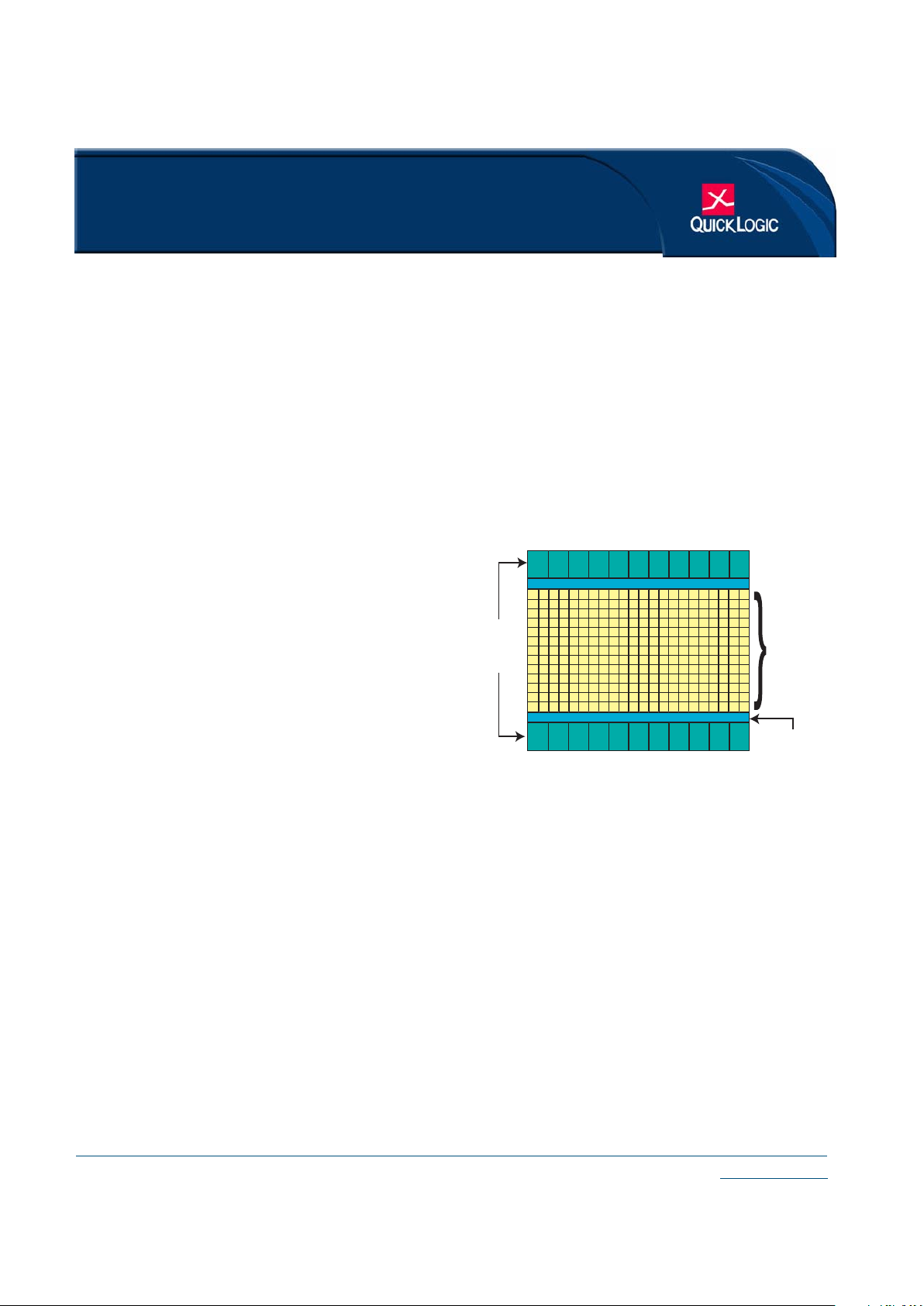
Figure 1: QuickRAM Block Diagram
22
RA M
Blocks
1,58 4
Hi gh Sp eed
Logic Cells
Interface
QL4090 QuickRAM Data Sheet
90,000 Usable PLD Gate QuickRAM ESP Combining Performance,
Density and Embedded RAM

2
www.quicklogic.com
© 2002 QuickLogic Corporation
•
•
•
•
•
•
QL4090 QuickRAM Data Sheet Rev H
Architecture Overview
The QuickRAMTM family of ESPs (Embedded Standard Products) offers FPGA logic in
combination with Dual-Port SRAM modules. The QL4090 is a 90,000 usable PLD gate
member of the QuickRAM family of ESPs. QuickRAM ESPs are fabricated on a 0.35 µm
four-layer metal process using QuickLogic's patented ViaLink
TM
technology to provide a
unique combination of high performance, high density, low cost, and extreme ease-of-use.
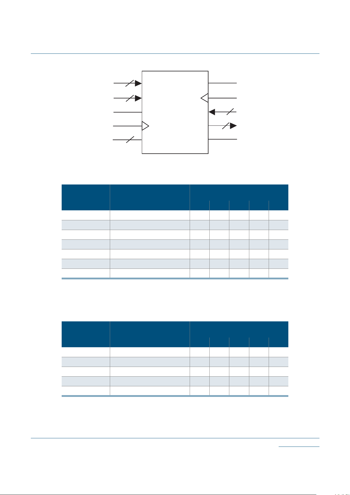
The QL4090 contains 1,584 logic cells and 22 Dual Port RAM modules (see Figure 1). Each
RAM module has 1,152 RAM bits, for a total of 25,344 bits. RAM Modules are Dual Port
(one read port, one write port) and can be configured into one of four modes: 64 (deep) x18
(wide), 128x9, 256x4, or 512x2 (see
Figure 4). With a maximum of 82 I/Os, the QL4090
is available in 208-pin PQFP, 208-pin CQFP 240-pin PQFP and 456-pin PBGA packages.
Designers can cascade multiple RAM modules to increase the depth or width allowed in
single modules by connecting corresponding address lines together and dividing the words
between modules (see
Figure 2). This approach allows up to 512-deep configurations as
large as 16 bits wide in the smallest QuickRAM device and 44 bits wide in the largest device.
Software support for the complete QuickRAM family, including the QL4090, is available
through two basic packages. The turnkey QuickWorks
TM
package provides the most
complete ESP software solution from design entry to logic synthesis, to place and route, to
simulation. The QuickTools
TM
packages provides a solution for designers who use Cadence,
Exemplar, Mentor, Synopsys, Synplicity, Viewlogic, Aldec, or other third-party tools for
design entry, synthesis, or simulation.
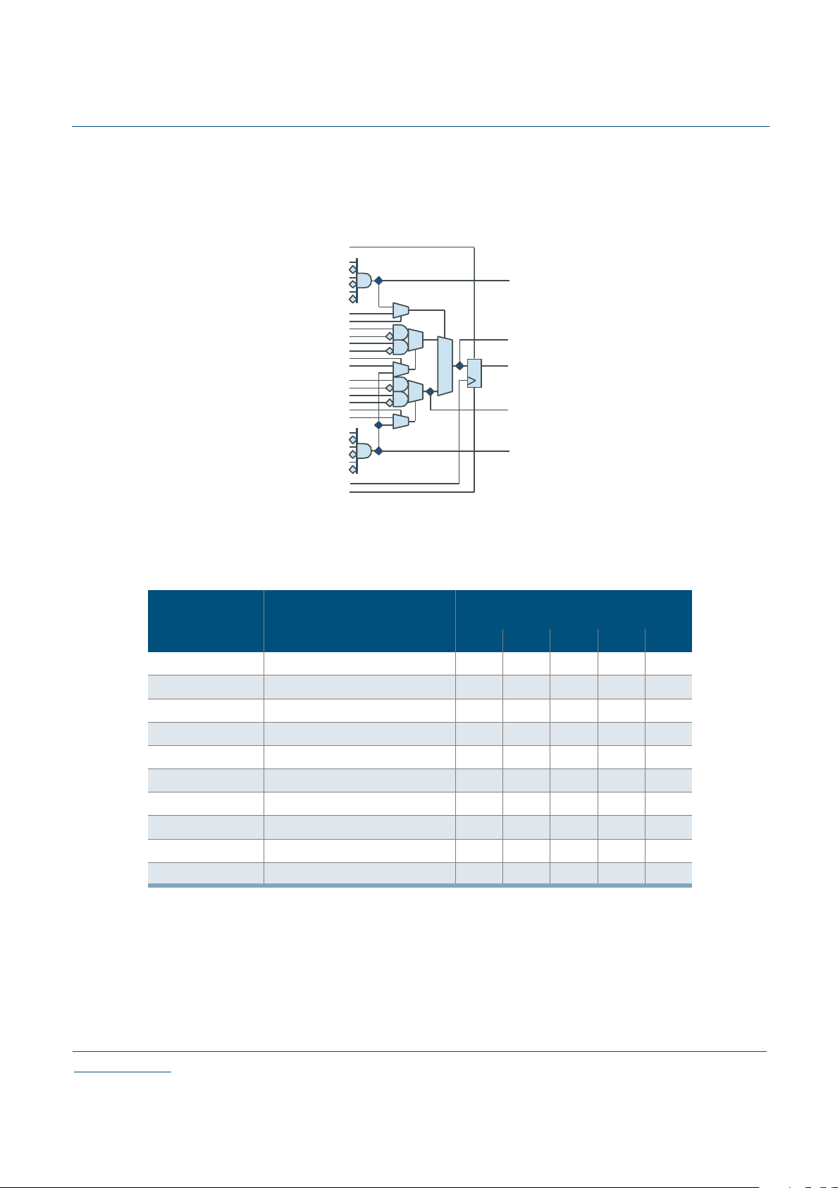
The QuickLogic variable grain logic cell features up to 16 simultaneous inputs and 5 outputs
within a cell that can be fragmented into 5 independent cells. Each cell has a fan-in of 29
including register and control lines (see
Figure 3).
Figure 2: QuickRAM Module Bits
RDATAWDATA
RADDR
RDATA
WADDR
WDATA
RAM
Module
(1,152 bits)
RAM
Module
(1,152 bits)

© 2002 QuickLogic Corporati on
www.quicklogic.com
3
•
•
•
•
•
•
QL4090 QuickRAM Data Sheet Rev H
Product Summary
Total of 316 I/O Pins
• 308 bi-directional input/output pins, PCI-compliant for 5.0 V and 3.3 V buses for
-1/-2/-3/-4 speed grades
• 8 high-drive input/distributed network pins
Eight Low-Skew Distributed Networks
• Two array clock/control networks available to the logic cell flip-flop clock, set and reset
inputs—each driven by an input-only pin
• Six global clock/control networks available to the logic cell F1, clock, set and reset inputs
and the input and I/O register clock, reset and enable inputs as well as the output enable
control—each driven by an input-only or I/O pin, or any logic cell output or I/O cell
feedback
High Performance Silicon
• Input + logic cell + output total delays under 6 ns
• Data path speeds over 400 MHz
• Counter speeds over 300 MHz
• FIFO speeds over 160+ MHz
4
www.quicklogic.com
© 2002 QuickLogic Corporation
•
•
•
•
•
•
QL4090 QuickRAM Data Sheet Rev H
AC Characteristics at VCC = 3.3 V, TA = 25° C (K = 1.00)
To calculate delays, multiply the appropriate K factor from Table 10: Operating Range by the
following numbers in the tables provided.
Figure 3: QuickRAM Logic Cell
Table 1: Logic Cell
Symbol Parameter
Propagation Delays (ns)
Fanout (5)
1 2 3 4 5
t
PD
Combinatorial Delay
a
a. These limits are derived from a representative selection of the slowest paths through the Quick-
RAM logic cell including typical net delays. Worst case delay values for specific paths should be
determined from timing analysis of your particular design.
1.4 1.7 1.9 2.2 3.2
t
SU
Setup Time
a
1.7 1.7 1.7 1.7 1.7
t
H
Hold Time 0.0 0.0 0.0 0.0 0.0
t
CLK
Clock to Q Delay 0.7 1.0 1.2 1.5 2.5
t
CWHI
Clock High Time 1.2 1.2 1.2 1.2 1.2
t
CWLO
Clock Low Time 1.2 1.2 1.2 1.2 1.2
t
SET
Set Delay 1.0 1.3 1.5 1.8 2.8
t
RESET
Reset Delay 0.8 1.1 1.3 1.6 2.6
t
SW
Set Width 1.9 1.9 1.9 1.9 1.9
t
RW
Reset Width 1.8 1.8 1.8 1.8 1.8
QS
A1
A2
A3
A4
A5
A6
F1
F2
F3
F4
F5
F6
QS
OP
B1
B2
C1
C2
MP
MS
D1
D2
E1
E2
NP
NS
QC
QR
OZ
AZ
QZ
NZ
FZ
© 2002 QuickLogic Corporati on
www.quicklogic.com
5
•
•
•
•
•
•
QL4090 QuickRAM Data Sheet Rev H
Figure 4: QuickRAM Module
Table 2: RAM Cell Synchronous Write Timing
Symbol Parameter
Propagation Delays (ns)
Fanout
1 2 3 4 5
t
SWA
WA Setup Time to WCLK 1.0 1.0 1.0 1.0 1.0
t
HWA
WA Hold Time to WCLK 0.0 0.0 0.0 0.0 0.0
t
SWD
WD Setup Time to WCLK 1.0 1.0 1.0 1.0 1.0
t
HWD
WD Hold Time to WCLK 0.0 0.0 0.0 0.0 0.0
t
SWE
WE Setup Time to WCLK 1.0 1.0 1.0 1.0 1.0
t
HWE
WE Hold Time to WCLK 0.0 0.0 0.0 0.0 0.0
t
WCRD
WCLK to RD (WA=RA)
a
a. Stated timing for worst case Propagation Delay over process variation at VCC = 3.3 V and
T
A
= 25° C. Multiply by the app ropriate Delay Factor, K, for speed gra de, voltage and tempe ratur e
settings as specified in the Operating Range.
5.0 5.3 5.6 5.9 7.1
Table 3: RAM Cell Synchronous Read Timing
Symbol Parameter
Propagation Delays (ns)
Fanout
Logic Cells 1 2 3 4 5
t
SRA
RA Setup Time to RCLK 1.0 1.0 1.0 1.0 1.0
t
HRA
RA Hold Time to RCLK 0.0 0.0 0.0 0.0 0.0
t
SRE
RE Setup Time to RCLK 1.0 1.0 1.0 1.0 1.0
t
HRE
RE Hold Time to RCLK 0.0 0.0 0.0 0.0 0.0
t
RCRD
RCLK to RD
a
a. Stated timing for worst case Propagation Delay over process variation at VCC = 3.3 V and
T
A
= 25° C. Multiply by the app ropriate Delay Factor, K, for speed gra de, voltage and tempe ratur e
settings as specified in the Operating Range.
4.0 4.3 4.6 4.9 6.1
WA
WD
WE
WCLK
RE
RCLK
RA
RD
[8:0]
[17:0]
[8:0]
[17:0 ]
MODE ASYNCRD
[1:0]
6
www.quicklogic.com
© 2002 QuickLogic Corporation
•
•
•
•
•
•
QL4090 QuickRAM Data Sheet Rev H
Table 4: RAM Cell Asynchronous Read Timing
Symbol Parameter
Propagation Delays (ns)
Fanout
1 2 3 4 5
RPDRD RA to RD
a
a. Stated timing for worst case Propagation Delay over process variation at VCC = 3.3 V and
T
A
= 25° C. Multiply by the app ropriate Delay Factor, K, for speed gra de, voltage and tempe ratur e
settings as specified in the Operating Range.
3.0 3.3 3.6 3.9 5.1
Table 5: Input-Only / Clock Cells
Symbol Parameter
Propagation Delays (ns)
Fanout
1 2 3 4 8 12 24
t
IN
High Drive Input Delay 1.5 1.6 1.8 1.9 2.4 2.9 4.4
t
INI
High Drive Input, Inverting Delay 1.6 1.7 .19 2.0 2.5 3.0 4.5
t
ISU
Input Register Set-Up Time 3.1 3.1 3.1 3.1 3.1 3.1 3.1
t
IH
Input Register Hold Time 0.0 0.0 0.0 0.0 0.0 0.0 0.0
t
ICLK
Input Register Clock To Q 0.7 0.8 1.0 1.1 1.6 2.1 3.6
t
IRST
Input Register Reset Delay 0.6 0.7 0.9 1.0 1.5 2.0 3.5
t
IESU
Input Register Clock Enable Setup Time 2.3 2.3 2.3 2.3 2.3 2.3 2.3
t
IEH
Input Register Clock Enable Hold Time 0.0 0.0 0.0 0.0 0.0 0.0 0.0
Table 6: Clock Cells
Symbol Parameter
Propagation Delays (ns)
Fanout
a
a. The array dist ribu ted ne tw ork s co nsi st of 40 ha lf columns and the glo bal d is tribu ted networks con-
sist of 44 half columns, each driven by an independent buffer. The number of half columns used
does not affect clock buffer delay. The array clock has up to 8 loads per half column. The global
clock has up to 11 loads per half column.
1 2 3 4 8 10 11
t
ACK
Array Clock Delay 1.2 1.2 1.3 1.3 1.5 1.6 1.7
t
GCKP
Global Clock Pin Delay 0.7 0.7 0.7 0.7 0.7 0.7 0.7
t
GCKB
Global Clock Buffer Delay 0.8 0.8 0.9 0.9 1.1 1.2 1.3
© 2002 QuickLogic Corporati on
www.quicklogic.com
7
•
•
•
•
•
•
QL4090 QuickRAM Data Sheet Rev H
Table 7: I/O Cell Input Delays
Symbol Parameter
Propagation Delays (ns)
Fanout
a
a. Stated timing for worst case Propagation Delay over process variation at V
CC
= 3.3 V and
T
A
= 25° C. Multiply by the ap prop ria te D e lay Fa cto r, K, for speed grade, vo ltage and temperature
settings as specified in the Operating Range.
1 2 3 4 8 10
t
I/O
Input Delay (bidirectional pad) 1.3 1.6 1.8 2.1 3.1 3.6
t
ISU
Input Register Set-Up Time 3.1 3.1 3.1 3.1 3.1 3.1
t
IH
Input Register Hold Time 0.0 0.0 0.0 0.0 0.0 0.0
t
IOCLK
Input Register Clock to Q 0.7 1.0 1.2 1.5 2.5 3.0
t
IORST
Input Register Reset Delay 0.6 0.9 1.1 1.4 2.4 2.9
t
IESU
Input Register Clock Enable Set-Up Time 2.3 2.3 2.3 2.3 2.3 2.3
t
IEH
Input Register Clock Enable Hold Time 0.0 0.0 0.0 0.0 0.0 0.0
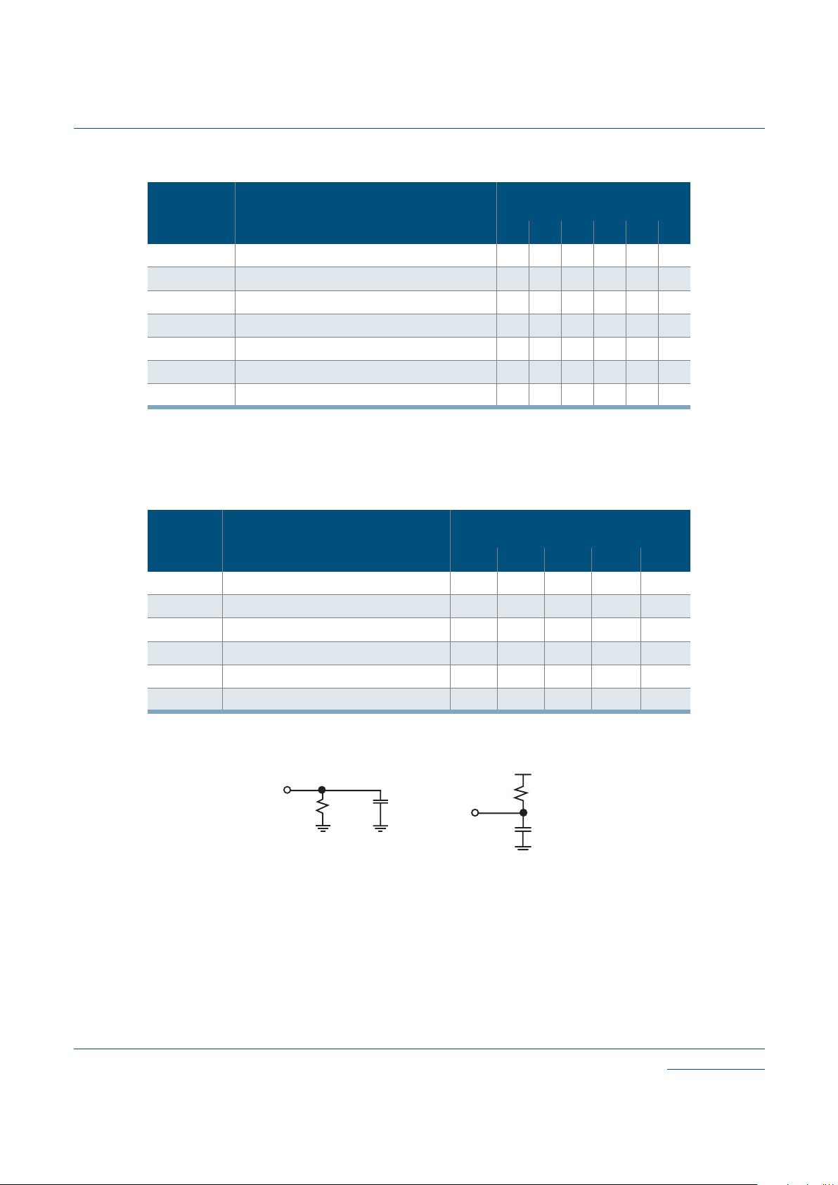
Table 8: I/O Cell Output Delays
Symbol Parameter
Propagation Delays (ns)
Output Load Capacitance (pF)
3 50 75 100 150
t
OUTLH
Output Delay Low to High 2.1 2.5 3.1 3.6 4.7
t
OUTHL
Output Delay High to Low 2.2 2.6 3.2 3.7 4.8
t
PZH
Output Delay Tri-state to High 1.2 1.7 2.2 2.8 3.9
t
PZL
Output Delay Tri-state to Low 1.6 2.0 2.6 3.1 4.2
t
PHZ
Output Delay High to Tri-state
a
a. The following loads are used for t
PXZ
2.0 - - - -
t
PLZ
Output Delay High to Tri-state
a
1.2 - - - -
1ΚΩ
1ΚΩ
tPHZ
tPLZ
5 pF
5 pF

8
www.quicklogic.com
© 2002 QuickLogic Corporation
•
•
•
•
•
•
QL4090 QuickRAM Data Sheet Rev H
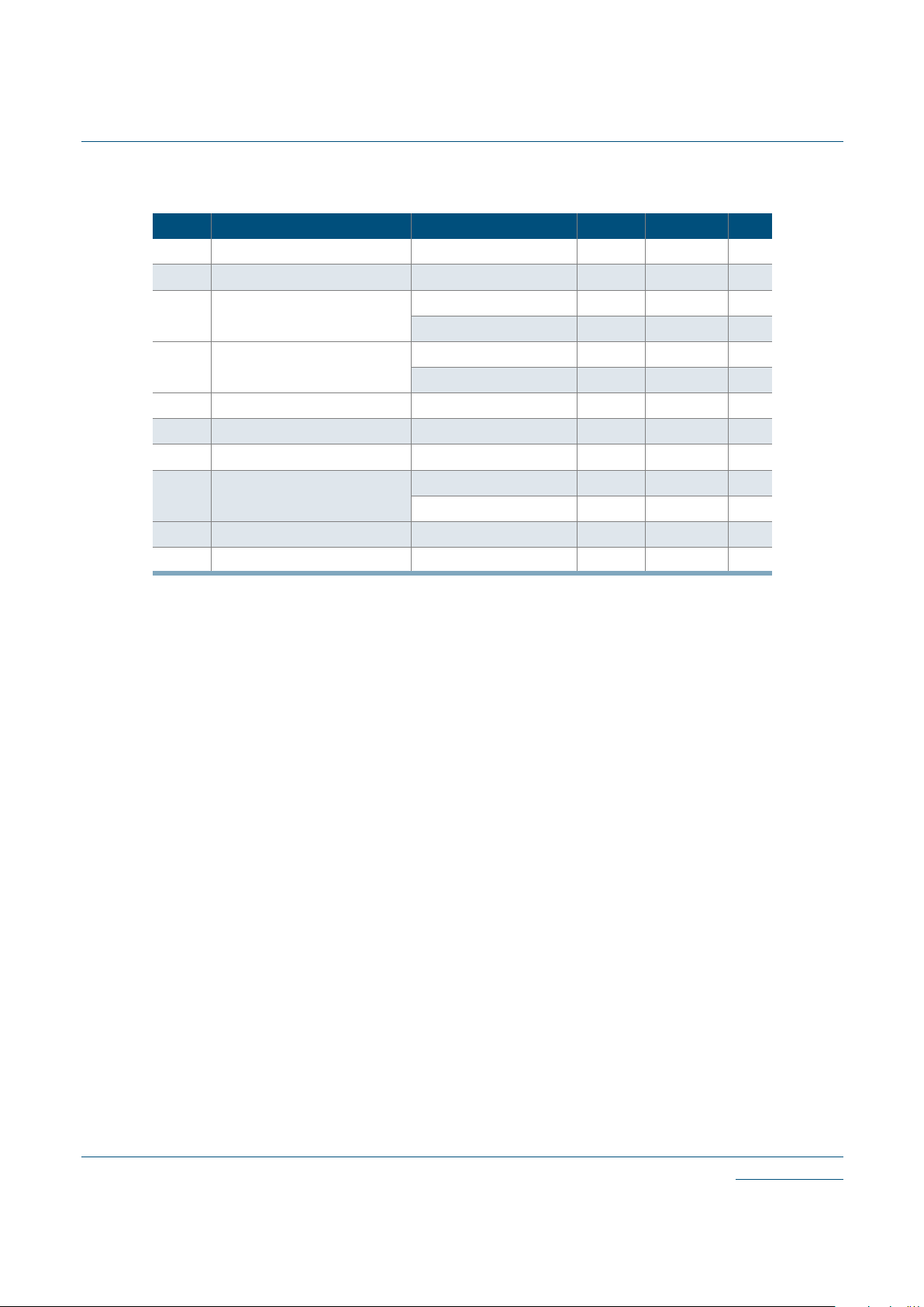
DC Characteristics
The DC specifications are provided in the tables below.
Table 9: Absolute Maximum Ratings
Parameter Value Parameter Value
VCC Voltage -0.5 to 4.6 V DC Input Current ±20 mA
V
CCIO
Voltage -0.5 to 7.0 V ESD Pad Protection ±2000 V
Input Voltage -0.5 V to V
CCIO
+0.5 V Storage Temperature -65° C to +150° C
Latch-up Immunity ±200 mA Lead Temperature 300° C
Table 10: Operating Range
Symbol Parameter Military Industrial Commercial Unit
Min Max Min Max Min Max
V
CC
Supply Voltage 3.0 3.6 3.0 3.6 3.0 3.6 V
V
CCIO
I/O Input Tolerance Voltage 3.0 5.5 3.0 5.5 3.0 5.25 V
T
A
Ambient Temperature -55 - -40 85 0 70 °C
T
C
Case Temperature - 125 - - - - °C
K Delay Factor
-0 Speed Grade 0.42 2.03 0.43 1.90 0.46 1.85 n/a
-1 Speed Grade 0.42 1.64 0.43 1.54 0.46 1.50 n/a
-2 Speed Grade 0.42 1.37 0.43 1.28 0.46 1.25 n/a
-3 Speed Grade 0.43 0.90 0.46 0.88 n/a
-4 Speed Grade 0.43 0.82 0.46 0.80 n/a
© 2002 QuickLogic Corporati on
www.quicklogic.com
9
•
•
•
•
•
•
QL4090 QuickRAM Data Sheet Rev H
Table 11: DC Characteristics
Symbol Parameter Conditions Min Max Units
V
IH
Input HIGH Voltage 0.5 VCCV
CCIO
+ 0.5 V
V
IL
Input LOW Voltage -0.5 0.3V
CC
V
V
OH
Output HIGH Voltage
IOH = -12 mA 2.4 V
IOH = -500 µA 0.9 V
CC
V
V
OL
Output LOW Voltage
IOL = 16 mA
a
a. Applies only to -1/-2/-3/-4 com mercial grade dev ices . These spee d gra des are also PCI-com plia nt. All
other devices have 8 mA IOL specifications.
0.45 V
IOL = 1.5 mA 0.1 V
CC
V
I
I
I or I/O Input Leakage Current VI = V
CCIO
or GND -10 10 µA
I
OZ
3-State Output Leakage Current VI = V
CCIO
or GND -10 10 µA
CIInput Capacitance
b
b. Capacitance is sample tested only. Clock pins are 12 pF maximum.
10 pF
I
OS
Output Short Circuit Current
c
c. Only one output at a time. Duration should not exceed 30 seconds.
VO = GND -15 -180 mA
VO = V
CC
40 210 mA
I
CC
D.C. Supply Current
d
d. For -1/-2/-3/-4 commercial grade devices only. Maximum ICC is 3 mA for -0 commercial grade and all
industrial grade devices . and 5 mA for all mil itary grade device s. For AC conditi ons, contact Qui ckLogic customer application s grou p.
VI, VIO = V
CCIO
or GND 0.50 (typ) 2 mA
I
CCIO
D.C. Supply Current on V
CCIO
0 100 µA

10
www.quicklogic.com
© 2002 QuickLogic Corporation
•
•
•
•
•
•
QL4090 QuickRAM Data Sheet Rev H
Kv and Kt Graphs
Figure 5: Voltage Factor vs. Supply Voltage
Figure 6: Temperature Factor vs. Operating Temperature
0.9200
0.9400
0.9600
0.9800
1.0000
1.0200
1.0400
1.0600
1.0800
1.1000
3 3.1 3.2 3.3 3.4 3.5 3 .6
Voltage Factor vs. Supply Voltage
Supply Voltage (V)
Kv
0.85
0.90
0.95
1.00
1.05
1.10
1.15
-60 -40 -20 0 20 40 60 80
Temper ature Factor vs. Ope ra ting Te mpe ra tur e
Junction Tem per ature C
Kt

© 2002 QuickLogic Corporati on
www.quicklogic.com
11
•
•
•
•
•
•
QL4090 QuickRAM Data Sheet Rev H
Power-up Sequencing
Figure 7: Power-up Requirements
The following requirements must be met when powering up the device:
(Refer to Figure 7 above)
• When ramping up the power supplies keep (V
CCIO
- VCC)
MAX
≤ 500 mV. Deviation from
this recommendation can cause permanent damage to the device.
• V
CCIO
must lead VCC when ramping the device.
• The power supply must take greater than or equal to 400 µs to reach V
CC
. Ramping to
V
CC/VCCIO
earlier than 400 µs can cause the device to behave improperly.
An internal diode is present in-between VCC and V
CCIO
, as shown in Figure 8.
Figure 8: Internal Diode Between VCC and V
CCIO
Voltage
V
CCIO
V
CC
(V
CCIO
-VCC)
MAX
Time
400 us
V
CC
V
CC
V
CCIO
Internal Logic
Cells, RAM
blocks, etc
IO Cells

12
www.quicklogic.com
© 2002 QuickLogic Corporation
•
•
•
•
•
•
QL4090 QuickRAM Data Sheet Rev H
JTAG
Figure 9: JTAG Block Diagram
Microprocessors and Application Specific Integrated Circuits (ASICs) pose many design
challenges, not the least of which concerns the accessibility of test points. The Joint Test
Access Group (JTAG) formed in response to this challenge, resulting in IEEE standard
1149.1, the Standard Test Access Port and Boundary Scan Architecture.
The JTAG boundary scan test methodology allows complete observation and control of the
boundary pins of a JTAG-compatible device through JTAG software. A Test Access Port
(TAP) controller works in concert with the Instruction Register (IR); these allow users to run
three required tests, along with several user-defined tests.
JTAG tests allow users to reduce system debug time, reuse test platforms and tools, and reuse
subsystem tests for fuller verification of higher level system elements.
TCK
TMS
TRSTB
RDI
TDO
Instruction Decode
&
Control Logic
TAp Controller
State Machine
(16 States)
Instruction Register
Boundary-Scan Register
(Data Register)
Mux
Bypass
Register
Mux
Internal
Register
I/O Registers
User Defined Data Register

© 2002 QuickLogic Corporati on
www.quicklogic.com
13
•
•
•
•
•
•
QL4090 QuickRAM Data Sheet Rev H
The 1149.1 standard requires the following three tests:
• Extest Instruction. The Extest instruction performs a PCB interconnect test. This test
places a device into an external boundary test mode, selecting the boundary scan
register to be connected between the TAP's Test Data In (TDI) and Test Data Out (TDO)
pins. Boundary scan cells are preloaded with test patterns (via the Sample/Preload
Instruction), and input boundary cells capture the input data for analysis.
• Sample/Preload Instruction. This instruction allows a device to remain in its
functional mode, while selecting the boundary scan register to be connected between
the TDI and TDO pins. For this test, the boundary scan register can be accessed via a
data scan operation, allowing users to sample the functional data entering and leaving
the device.
• Bypass Instruction. The Bypass instruction allows data to skip a device's boundary
scan entirely, so the data passes through the bypass register. The Bypass instruction
allows users to test a device without passing through other devices. The bypass register
is connected between the TDI and TDO pins, allowing serial data to be transferred
through a device without affecting the operation of the device.
14
www.quicklogic.com
© 2002 QuickLogic Corporation
•
•
•
•
•
•
QL4090 QuickRAM Data Sheet Rev H
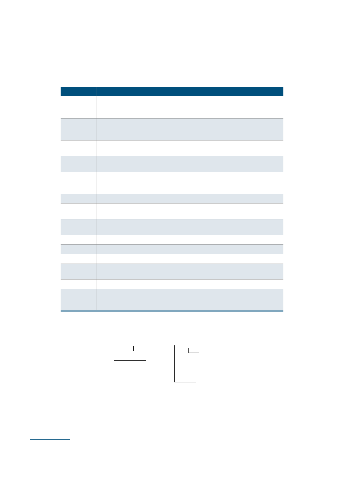
Pin Descriptions
Ordering Information
Table 12: Pin Descriptions
Pin Function Description
TDI/RSI
Test Data In for JTAG /RAM
init. Serial Data In
Hold HIGH during normal operation. Connects to
serial PROM data in for RAM initialization. Connect
to V
CC
if unused.
TRSTB/RRO
Active low Reset for JTAG
/RAM init. reset out
Hold LOW during normal operation. Connects to
serial PROM reset for RAM initialization. Connect to
GND if unused.
TMS Test Mode Select for JTAG
Hold HIGH during normal operation. Connect to
V
CC
if not used for JTAG.
TCK Test Clock for JTAG
Hold HIGH or LOW during normal operation.
Connect to V
CC
or ground if not used for JTAG.
TDO/RCO
Test data out for JTAG /RAM
init. clock out
Connect to serial PROM clock for RAM
initialization. Must be left unconnected if not used for
JTAG or RAM initialization.
STM Special Test Mode Must be grounded during normal operation.
I/ACLK
High-drive input and/or array
network driver
Can be configured as either or both.
I/GCLK
High-drive input and/or global
network driver
Can be configured as either or both.
I High-drive input Use for input signals with high fanout.
I/O Input/Output pin Can be configured as an input and/or output.
V
CC
Power supply pin Connect to 3.3 V supply.
V
CCIO
Input voltage tolerance pin
Connect to 5.0 V supply if 5 V input tolerance is
required, otherwise connect to 3.3 V supply.
GND Ground pin Connect to ground.
GND/THERM Ground/Thermal pin
Available on 456-PBGA only. Connect to ground
plane on PCB if heat sinking desired. Otherwise may
be left unconnected.
QL 4090 - 1 PQ208 C
QuickLogic device
QuickRAM device
part number
Speed Grade
0 = Quick
1 = Fast
2 = Faster
3 = Faster
*4 = Wow
Operating Range
C = Commercial
I = Industrial
M = Military
Package Code
PQ208 = 208-pin PQFP
CF208 = 208-pin CQFP
PQ240 = 240-pin PQFP
PB456 = 456-pin PBGA
* Contact QuickLogic regarding availabliity

© 2002 QuickLogic Corporati on
www.quicklogic.com
15
•
•
•
•
•
•
QL4090 QuickRAM Data Sheet Rev H
208 and 240 PQFP Pinout Diagrams
Figure 10: Top View of 208 Pin PQFP/CQFP
Figure 11: Top View of 240 Pin PQFP
Pin 1
Pin 53 Pin 105
Pin 157
QL4090-1PQ208C
QuickRAM
Pin 1
Pin 61
Pin 121
Pin 181
QL4090-1PQ240C
QuickRAM
16
www.quicklogic.com
© 2002 QuickLogic Corporation
•
•
•
•
•
•
QL4090 QuickRAM Data Sheet Rev H
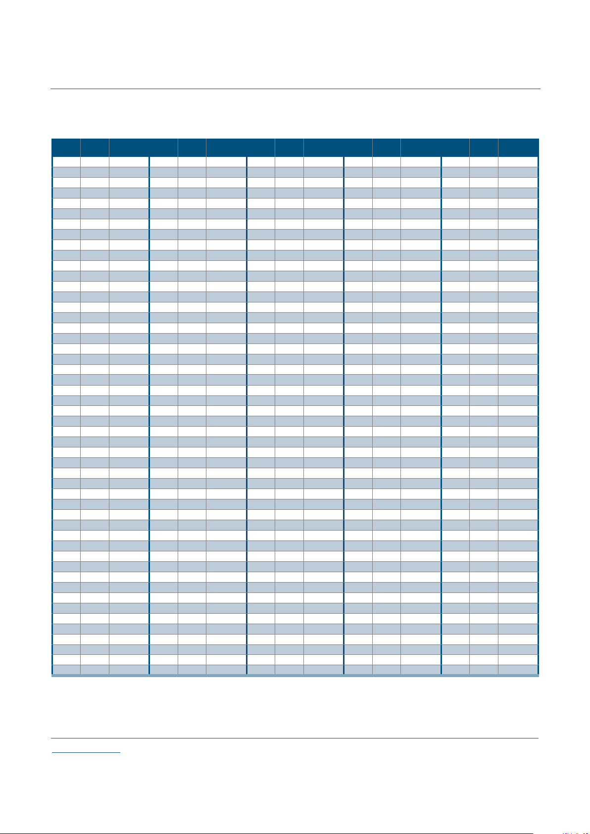
208 and 240 PQFP Pinout Table
Table 13: 208/240 PQFP Pinout Table
240
PQFP
208
PQFP
Function
240
PQFP
208
PQFP
Function
240
PQFP
208
PQFP
Function
240
PQFP
208
PQFP
Function
240
PQFP
208
PQFP
Function
1208
I/O
51 43
GND
98 84
I/O
145 125
I/O
194 168
I/O
2 1
I/O
52 44
I/O
99 85
I/O
146 126
I/O
195 169
I/O
32
I/O
53 45
I/O
100 86
I/O
147 127
GND
196 NC
I/O
4 3
I/O
54 46
I/O
101 87
I/O
148 128
I/O
197 170
I/O
54
I/O
55 47
I/O
102 88
I/O
149 NC
I/O
198 171
I/O
6 5
I/O
56 48
I/O
103 89
I/O
150 129
GLCK/I
199 172
I/O
7NC
I/O
57 NC
I/O
104 90
I/O
151 130
ACLK/I
200 173
I/O
8 6
I/O
58 49
I/O
105 91
I/O
152 131
V
CC
201 174
I/O
97
I/O
59 50
I/O
106 92
I/O
153 132
GLCK/I
202 175
I/O
10 8
I/O
60 51
I/O
107 NC
I/O
154 133
GLCK/I
203 NC
I/O
11 9
I/O
NC 52
I/O
108 93
I/O
155 134
V
CC
204 176
I/O
12 10
V
CC
NC 53
I/O
109 94
I/O
156 135
I/O
205 177
GND
13 11
I/O
61 54
TDI
110 95
GND
157 136
I/O
206 178
I/O
14 12
GND
62 NC
I/O
NC 96
I/O
158 NC
I/O
207 179
I/O
15 13
I/O
63 NC
I/O
111 97
V
CC
159 137
I/O
208 NC
I/O
16 14
I/O
64 55
I/O
NC 98
I/O
160 NC
GND
209 180
I/O
17 NC
I/O
65 56
I/O
NC 99
I/O
161 138
I/O
210 181
I/O
18 15
I/O
66 NC
I/O
112 100
I/O
162 139
I/O
211 182
GND
19 16
I/O
67 57
I/O
113 NC
I/O
163 140
I/O
212 NC
V
CC
20 17
I/O
68 58
I/O
114 101
I/O
164 141
I/O
213 183
I/O
21 18
I/O
69 59
GND
115 NC
I/O
165 142
I/O
214 184
I/O
22 19
I/O
70 60
I/O
116 102
I/O
166 NC
I/O
215 185
I/O
23 20
I/O
71 61
V
CC
117 NC
I/O
167 143
I/O
216 186
I/O
24 NC
I/O
72 62
I/O
118 NC
I/O
168 144
I/O
217 187
V
CCIO
25 21
I/O
73 63
I/O
119 103
TRSTB
169 145
V
CC
218 188
I/O
26 22
I/O
74 64
I/O
120 104
TMS
170 NC
I/O
219 NC
I/O
27 23
GND
75 NC
I/O
121 105
I/O
171 146
I/O
220 189
I/O
28 24
I/O
76 65
I/O
122 NC
I/O
172 147
GND
221 190
I/O
29 25
GCLK/I
77 66
I/O
123 106
I/O
173 148
I/O
222 191
I/O
30 26
ACLK/I
78 67
I/O
124 107
I/O
174 149
I/O
223 192
I/O
31 27
V
CC
79 NC
I/O
125 108
I/O
175 150
I/O
224 193
I/O
32 28
GCLK/I
80 68
I/O
126 109
I/O
176 151
I/O
225 194
I/O
33 29
GCLK/I
81 69
I/O
127 NC
I/O
177 152
I/O
226 NC
I/O
34 30
V
CC
82 70
I/O
128 110
I/O
178 153
I/O
227 195
I/O
35 31
I/O
83 NC
I/O
129 111
I/O
179 154
I/O
228 196
I/O
36 32
I/O
NC 71
I/O
130 112
I/O
180 155
I/O
229 197
I/O
37 NC
GND
84 NC
I/O
131 113
I/O
NC 156
I/O
230 198
I/O
38 33
I/O
85 72
I/O
132 114
V
CC
181 157
TCK
231 NC
I/O
39 NC
I/O
86 73
GND
133 115
I/O
182 158
STM
232 199
GND
40 34
I/O
87 74
I/O
134 116
GND
183 NC
I/O
233 200
I/O
41 35
I/O
88 NC
V
CC
135 117
I/O
184 159
I/O
234 201
V
CC
42 36
I/O
89 75
I/O
136 NC
I/O
185 160
I/O
235 202
I/O
43 NC
I/O
90 76
I/O
137 118
I/O
186 161
I/O
236 203
I/O
44 37
I/O
91 77
I/O
138 119
I/O
187 162
I/O
237 204
I/O
45 38
I/O
92 78
GND
139 120
I/O
188 163
GND
238 205
I/O
46 39
I/O
93 79
I/O
140 121
I/O
189 164
I/O
239 206
I/O
47 NC
I/O
94 80
I/O
141 NC
I/O
190 165
V
CC
240 207
TDO
48 40
I/O
95 81
I/O
142 122
I/O
191 166
I/O
49 41
V
CC
96 82
I/O
143 123
I/O
192 NC
I/O
50 42
I/O
97 83
V
CCIO
144 124
I/O
193 167
I/O
© 2002 QuickLogic Corporati on
www.quicklogic.com
17
•
•
•
•
•
•
QL4090 QuickRAM Data Sheet Rev H
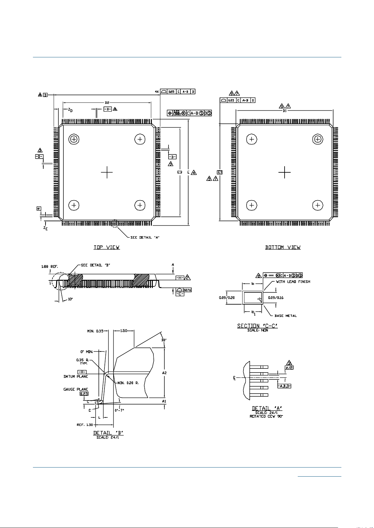
208 and 240 PQFP Mechanical Drawing
Figure 12: 208 PQFP Mechanical Drawing
18
www.quicklogic.com
© 2002 QuickLogic Corporation
•
•
•
•
•
•
QL4090 QuickRAM Data Sheet Rev H
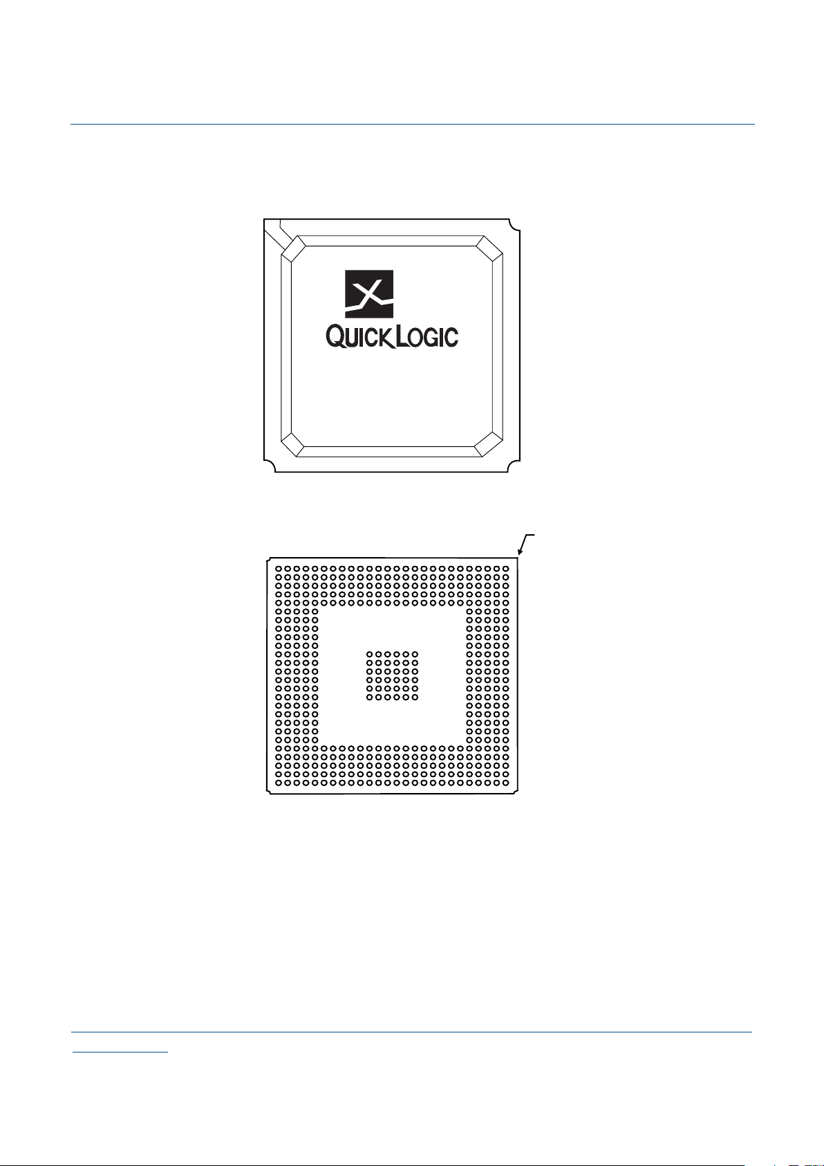
456 PBGA Pinout Diagram
Figure 13: 456 PBGA Pinout Diagram
QL4090-1PB456C
QuickRAM
BOTTOM View
TOP View
PIN A1
CORNER
26 25 24 23 22 21 20 19 18 17 16 15 14 13 12 11 10 9 8 7 6 5 4 3 2 1
A
B
C
D
E
F
G
H
J
K
L
M
N
P
R
T
U
V
W
Y
AA
AB
AC
AD
AE
AF

© 2002 QuickLogic Corporati on
www.quicklogic.com
19
•
•
•
•
•
•
QL4090 QuickRAM Data Sheet Rev H
456 PBGA Pinout Table
Table 14: 456 PBGA Pinout Table
456 Function 456 Function 456 Function 456 Function 456 Function
A1
I/O
C1
I/O
E1
I/O
H23
I/O
M23
NC
A2
I/O
C2
I/O
E2
I/O
H24
I/O
M24
I/O
A3
I/O
C3
I/O
E3
I/O
H25
I/O
M25
I/O
A4
I/O
C4
TDO
E4
I/O
H26
I/O
M26
I/O
A5
I/O
C5
I/O
E5
GND
J1
I/O
N1
GCLK/I
A6
I/O
C6
I/O
E6
V
CC
J2
I/O
N2
I/O
A7
I/O
C7
I/O
E7
GND
J3
I/O
N3
I/O
A8
I/O
C8
I/O
E8
NC
J4
NC
N4
GCLK/I
A9
I/O
C9
I/O
E9
GND
J5
GND
N5
V
CC
A10
I/O
C10
I/O
E10
I/O
J22
NC
N11
GND/THERM
A11
I/O
C11
I/O
E11
GND
J23
NC
N12
GND/THERM
A12
V
CCIO
C12
I/O
E12
GND
J24
I/O
N13
GND/THERM
A13
I/O
C13
I/O
E13
V
CC
J25
I/O
N14
GND/THERM
A14
I/O
C14
I/O
E14
GND
J26
I/O
N15
GND/THERM
A15
I/O
C15
I/O
E15
GND
K1
I/O
N16
GND/THERM
A16
I/O
C16
I/O
E16
GND
K2
I/O
N22
GND
A17
I/O
C17
I/O
E17
NC
K3
I/O
N23
I/O
A18
I/O
C18
I/O
E18
GND
K4
I/O
N24
I/O
A19
I/O
C19
I/O
E19
NC
K5
V
CC
N25
I/O
A20
I/O
C20
I/O
E20
GND
K22
GND
N26
I/O
A21
I/O
C21
I/O
E21
V
CC
K23
I/O
P1
I/O
A22
I/O
C22
I/O
E22
GND
K24
I/O
P2
I/O
A23
I/O
C23
I/O
E23
I/O
K25
I/O
P3
I/O
A24
I/O
C24
I/O
E24
I/O
K26
I/O
P4
I/O
A25
I/O
C25
TCK
E25
I/O
L1
I/O
P5
NC
A26
I/O
C26
I/O
E26
I/O
L2
I/O
P11
GND/THERM
B1
I/O
D1
I/O
F1
I/O
L3
I/O
P12
GND/THERM
B2
I/O
D2
I/O
F2
I/O
L4
I/O
P13
GND/THERM
B3
I/O
D3
I/O
F3
I/O
L5
NC
P14
GND/THERM
B4
I/O
D4
GND
F4
NC
L11
GND/THERM
P15
GND/THERM
B5
I/O
D5
I/O
F5
V
CC
L12
GND/THERM
P16
GND/THERM
B6
I/O
D6
NC
F22
V
CC
L13
GND/THERM
P22
NC
B7
I/O
D7
I/O
F23
NC
L14
GND/THERM
P23
GCLK / I
B8
I/O
D8
I/O
F24
I/O
L15
GND/THERM
P24
GCLK / I
B9
I/O
D9
GND
F25
I/O
L16
GND/THERM
P25
I/O
B10
I/O
D10
I/O
F26
I/O
L22
NC
p26
ACLK/I
B11
I/O
D11
I/O
G1
I/O
L23
I/O
R1
I/O
B12
I/O
D12
GND
G2
I/O
L24
I/O
R2
I/O
B13
I/O
D13
I/O
G3
I/O
L25
I/O
R3
I/O
B14
I/O
D14
I/O
G4
I/O
L26
I/O
R4
NC
B15
I/O
D15
GND
G5
NC
M1
ACLK / I
R5
NC
B16
I/O
D16
I/O
G22
GND
M2
GCLK/I
R11
GND/THERM
B17
I/O
D17
I/O
G23
I/O
M3
I/O
R12
GND/THERM
B18
I/O
D18
GND
G24
I/O
M4
NC
R13
GND/THERM
B19
I/O
D19
I/O
G25
I/O
M5
GND
R14
GND/THERM
B20
I/O
D20
I/O
G26
I/O
M11
GND/THERM
R15
GND/THERM
B21
I/O
D21
NC
H1
I/O
M12
GND/THERM
R16
GND/THERM
B22
I/O
D22
I/O
H2
I/O
M13
GND/THERM
R22
V
CC
B23
I/O
D23
GND
H3
I/O
M14
GND/THERM
R23
NC
B24
I/O
D24
I/O
H4
I/O
M15
GND/THERM
R24
I/O
B25
I/O
D25
I/O
H5
NC
M16
GND/THERM
R25
I/O
B26
STM
D26
I/O
H22
NC
M22
NC
R26
GCLK / I
(Sheet 1 of 2)
20
www.quicklogic.com
© 2002 QuickLogic Corporation
•
•
•
•
•
•
QL4090 QuickRAM Data Sheet Rev H
T1
I/O
W5
NC
AB15
V
CC
AD3
I/O
AE17
I/O
T2
I/O
W22
NC
AB16
I/O
AD4
I/O
AE18
I/O
T3
I/O
W23
I/O
AB17
NC
AD5
I/O
AE19
I/O
T4
I/O
W24
I/O
AB18
V
CC
AD6
I/O
AE20
I/O
T5
V
CC
W25
I/O
AB19
GND
AD7
I/O
AE21
I/O
T11
GND/THERMAL
W26
I/O
AB20
NC
AD8
I/O
AE22
I/O
T12
GND/THERMAL
Y1
I/O
AB21
V
CC
AD9
I/O
AE23
NC
T13
GND/THERMAL
Y2
I/O
AB22
GND
AD10
I/O
AE24
TMS
T14
GND/THERMAL
Y3
I/O
AB23
I/O
AD11
I/O
AE25
I/O
T15
GND/THERMAL
Y4
I/O
AB24
I/O
AD12
I/O
AE26
I/O
T16
GND/THERMAL
Y5
I/O
AB25
I/O
AD13
I/O
AF1
I/O
T22
GND
Y22
GND
AB26
I/O
AD14
I/O
AF2
I/O
T23
I/O
Y23
I/O
AC1
I/O
AD15
I/O
AF3
I/O
T24
I/O
Y24
I/O
AC2
I/O
AD16
I/O
AF4
I/O
T25
I/O
Y25
I/O
AC3
NC
AD17
I/O
AF5
I/O
T26
I/O
Y26
I/O
AC4
GND
AD18
I/O
AF6
I/O
U1
I/O
AA1
I/O
AC5
I/O
AD19
I/O
AF7
I/O
U2
I/O
AA2
I/O
AC6
NC
AD20
I/O
AF8
I/O
U3
I/O
AA3
NC
AC7
I/O
AD21
I/O
AF9
I/O
U4
I/O
AA4
NC
AC8
I/O
AD22
I/O
AF10
I/O
U5
GND
AA5
V
CC
AC9
NC
AD23
TRSTB
AF11
I/O
U22
NC
AA22
V
CC
AC10
I/O
AD24
I/O
AF12
I/O
U23
I/O
AA23
NC
AC11
I/O
AD25
I/O
AF13
I/O
U24
I/O
AA24
I/O
AC12
NC
AD26
I/O
AF14
I/O
U25
I/O
AA25
I/O
AC13
I/O
AE1
TDI
AF15
I/O
U26
I/O
AA26
I/O
AC14
V
CCIO
AE2
I/O
AF16
I/O
V1
I/O
AB1
I/O
AC15
NC
AE3
I/O
AF17
I/O
V2
I/O
AB2
I/O
AC16
I/O
AE4
I/O
AF18
I/O
V3
I/O
AB3
I/O
AC17
I/O
AE5
I/O
AF19
I/O
V4
NC
AB4
I/O
AC18
NC
AE6
I/O
AF20
I/O
V5
NC
AB5
GND
AC19
I/O
AE7
I/O
AF21
I/O
V22
GND
AB6
V
CC
AC20
I/O
AE8
I/O
AF22
I/O
V23
NC
AB7
NC
AC21
I/O
AE9
I/O
AF23
I/O
V24
I/O
AB8
NC
AC22
NC
AE10
I/O
AF24
I/O
V25
I/O
AB9
NC
AC23
GND
AE11
I/O
AF25
I/O
V26
I/O
AB10
V
CC
AC24
I/O
AE12
I/O
AF26
I/O
W1
I/O
AB11
GND
AC25
I/O
AE13
I/O
W2
I/O
AB12
NC
AC26
I/O
AE14
I/O
W3
I/O
AB13
I/O
AD1
I/O
AE15
I/O
W4
I/O
AB14
GND
AD2
NC
AE16
I/O
Table 14: 456 PBGA Pinout Table (Continued)
456 Function 456 Function 456 Function 456 Function 456 Function
(Sheet 2 of 2)
© 2002 QuickLogic Corporati on
www.quicklogic.com
21
•
•
•
•
•
•
QL4090 QuickRAM Data Sheet Rev H
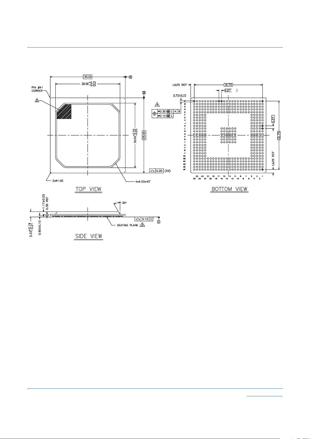
456 PBGA Mechanical Drawing
Figure 14: 456 PBGA Mechanical Drawing
22
www.quicklogic.com
© 2002 QuickLogic Corporation
•
•
•
•
•
•
QL4090 QuickRAM Data Sheet Rev H
Contact Information
Telephone: 408 990 4000 (US)
416 497 8884 (Canada)
44 1932 57 9011 (Europe)
49 89 930 86 170 (Germany)
852 8106 9091 (Asia)
81 45 470 5525 (Japan)
E-mail: info@quicklogic.com
Support: support@quicklogic.com
Web site: http://www.quicklogic.com/
Revision History
Copyright Information
Copyright © 2002 QuickLogic Corporation. All Rights Reserved.
The information contained in this product brief, and the accompanying software programs
are protected by copyright. All rights are reserved by QuickLogic Corporation. QuickLogic
Corporation reserves the right to make periodic modifications of this product without
obligation to notify any person or entity of such revision. Copying, duplicating, selling, or
otherwise distributing any part of this product without the prior written consent of an
authorized representative of QuickLogic is prohibited.
QuickLogic, pASIC, and ViaLink are registered trademarks, and SpDE and QuickWorks are
trademarks of QuickLogic Corporation.
Verilog is a registered trademark of Cadence Design Systems, Inc.
Table 15: Revision History
Revision Date Comments
A not avail. First release.
B not avail.
C not avail.
D not avail.
E not avail.
F May 2000
G April 2002 Update of AC/DC Specs and reformat
H May 2002
Added Kfactor, Power-up, JTAG and mechanical
drawing information. Reformatted.
 Loading...