

QUICK LOGIC QL6325-5PT280M, QL6325-6PS484C, QL6325-6PS484I, QL6325-6PS484M, QL6325-6PS516C Datasheet
...
© 2002 QuickLogic Corporati on
www.quicklogic.com
1
•
•
•
•
•
•
• • • • • •
Device Highlights
Flexible Programmable Logic
• .25
µ
m, Five layer metal CMOS Process
• 2.5 V V
CC
, 2.5 V/3.3 V Drive Capable I/O
• 1,536 Logic Cells
• 320,640 Max System Gates
• Up to 313 I/O Pins
Embedded Dual Port SRAM
• Twenty four 2,304-bit Dual Port High
Performance SRAM Blocks
• 55,300 RAM Bits
• RAM/ROM/FIFO Wizard for Automatic
Configuration
• Configurable and Cascadable
Programmable I/O
• High performance Enhanced I/O (EIO):
Less than 3 ns Tco
• Programmable Slew Rate Control
• Programmable I/O Standards:
• LVTTL, LVCMOS, PCI, GTL+, SSTL2,
and SSTL3
• Eight Independent I/O Banks
• Three Register Configurations: Input,
Output, and Output Enable
Advanced Clock Network
• Nine Global Clock Networks:
• One Dedicated
• Eight Programmable
• 20 Quad-Net Networks: Five per Quadrant
• 16 I/O Controls: Two per I/O Bank
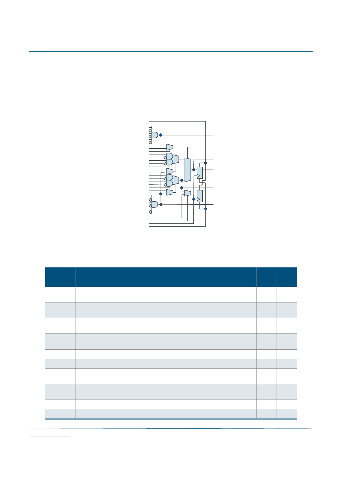
Figure 1: Eclipse Block Diagram
Memory - Dual Port RAM
High Speed Logic Cells
321K Gates
Memory - Dual Port RAM
Combining Performance, Density, and Embedded RAM
QL6325 Eclipse Data Sheet
2
www.quicklogic.com
© 2002 QuickLogic Corporation
•
•
•
•
•
•
QL6325 Eclipse Data Sheet Rev C
Electrical Specifications
AC Characteristic s a t VCC = 2.5 V, TA = 25° C (K = 0.74)
The AC Specifications are provided from Table 1 to Table 10. Logic Cell diagrams and
waveforms are provided from
Figure 2 to Figure 15.
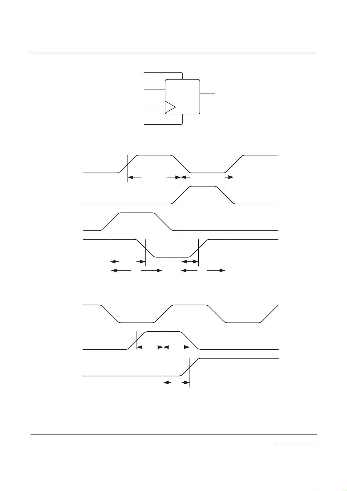
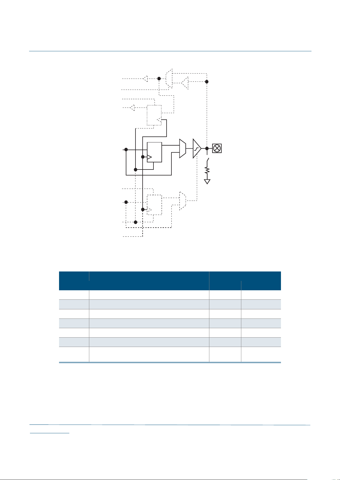
Figure 2: Eclipse Logic Cell
Table 1: Logic Cells
Symbol Parameter Value (ns)
Logic Cells Min Max
t
PD
Combinatorial Delay of the longest path: time taken by the combinatorial circuit to
output
- 0.257
t
SU
Setup time: time the synchronous input of the flip flop must be stable before the
active clock edge
0.22 -
t
HL
Hold time: time the synchronous input of the flip flop must be stable after the active
clock edge
0 -
t
CO
Clock-to-out delay: the amount of time taken by the flip flop to output after the
active clock edge.
- 0.255
t
CWHI
Clock High Time: required minimum time the clock stays high 0.46 -
t
CWLO
Clock Low Time: required minimum time that the clock stays low 0.46 -
t
SET
Set Delay: time between when the flip flop is ”set” (high)
and when the output is consequently “set” (high)
- 0.18
t
RESET
Reset Delay: time between when the flip flop is ”reset” (low) and when the output
is consequently “reset” (low)
- 0.09
t
SW
Set Width: time that the SET signal remains high/low 0.3 -
t
RW
Reset Width: time that the RESET signal remains high/low 0.3 -
© 2002 QuickLogic Corporati on
www.quicklogic.com
3
•
•
•
•
•
•
QL6325 Eclipse Data Sheet Rev C
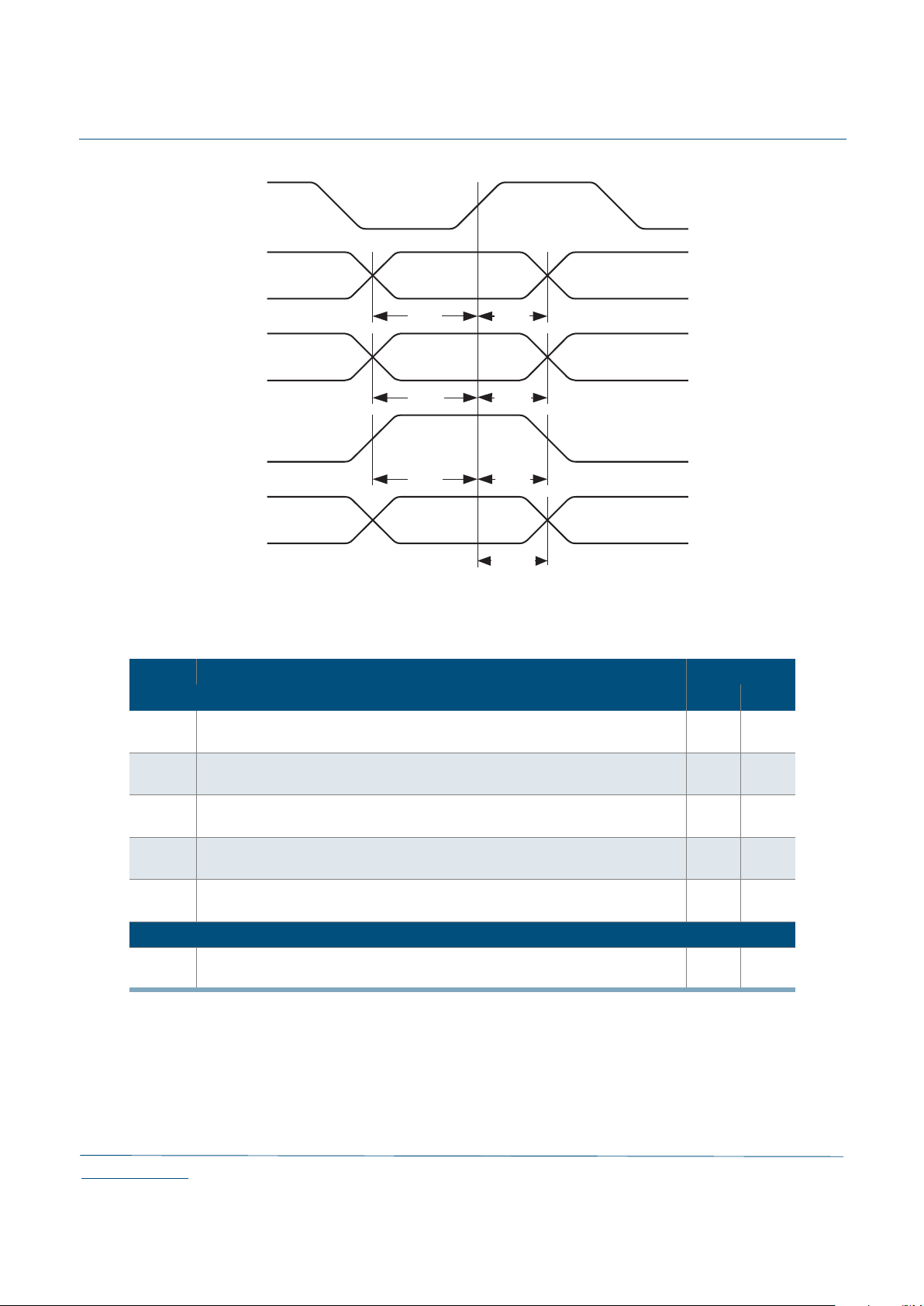
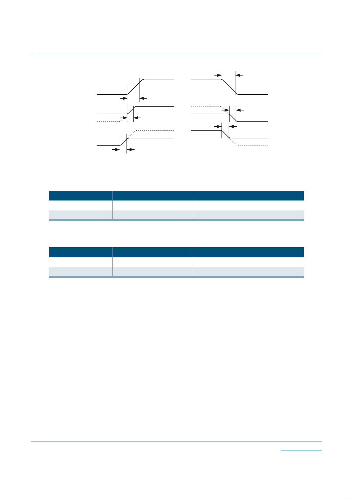
Figure 3: Logic Cell Flip Flop
Figure 4: Logic Cell Flip Flop Timings - First Waveform
Figure 5: Logic Cell Flip Flop Timings - Second Waveform
SET
D
CLK
RESET
Q
SET
RESET
Q
CLK
t
CWHI
(min)
t
CWLO
(min)
t
RESET
t
RW
t
SET
t
SW
CLK
D
Q
t
SU
t
HL
t
CO
4
www.quicklogic.com
© 2002 QuickLogic Corporation
•
•
•
•
•
•
QL6325 Eclipse Data Sheet Rev C
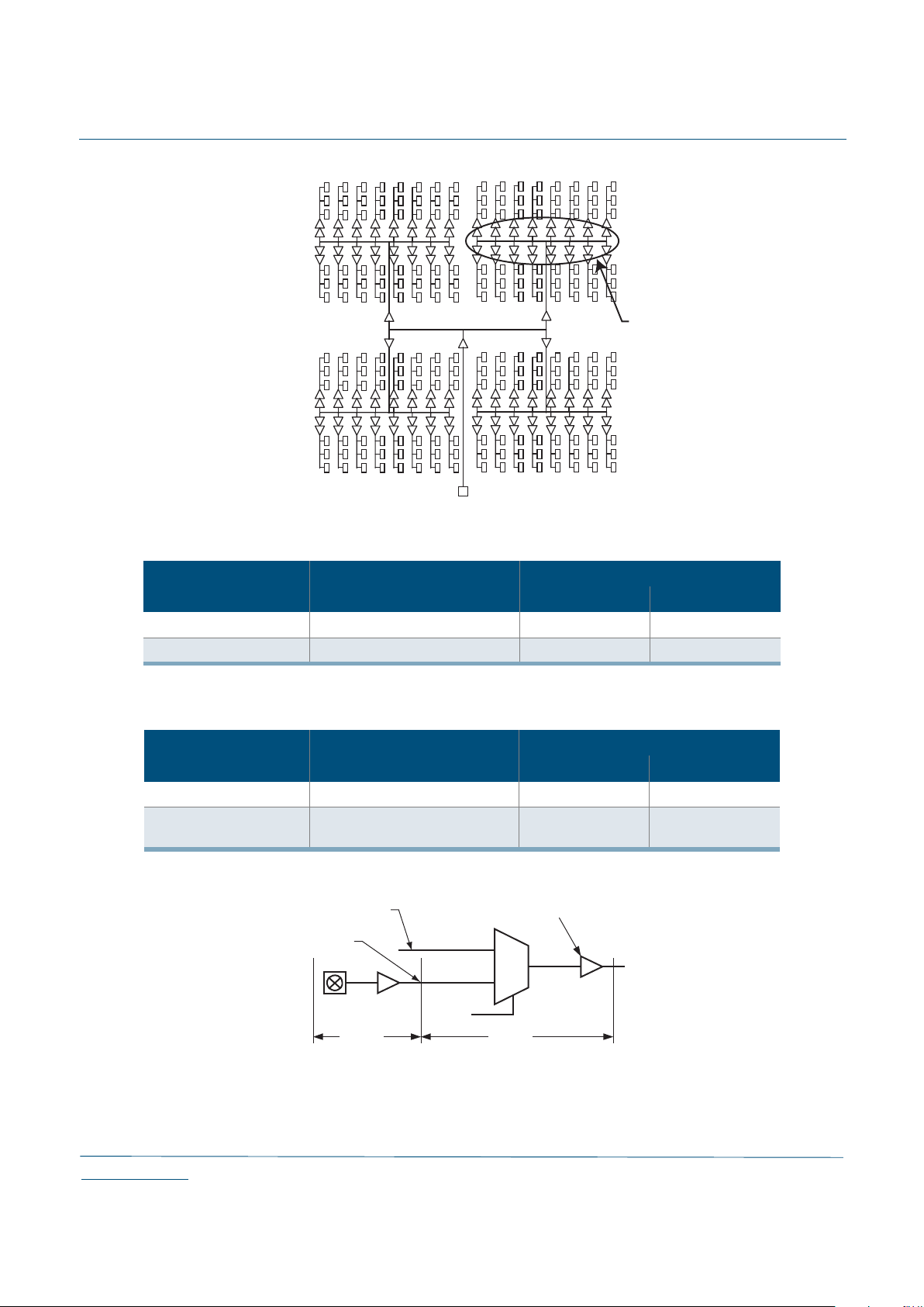
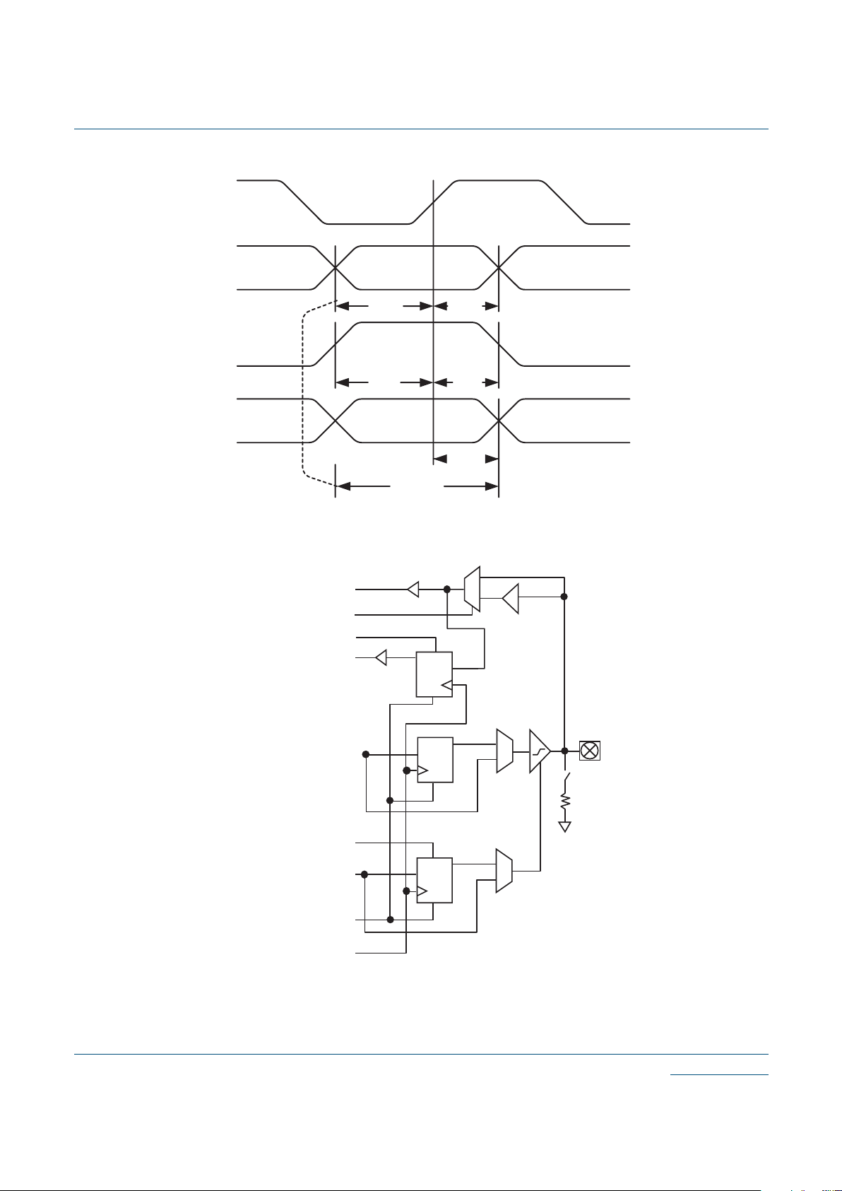
Figure 6: Eclipse Global Clock Structure
Figure 7: Global Clock Structure Schematic
Table 2: Eclipse Clock Performance
Clock Parameters Clock Performance
Global Dedicated
Logic Cells (Internal) Clock signal generated internally 1.51 ns (max) 1.59 ns (max)
I/O’s (External) Clock signal generated externally 2.06 ns (max) 1.73 ns (max)
Table 3: Eclipse Global Clock Performance
Clock Segment Parameter Value (ns)
Min Max
t
PGCK
Global clock pin delay to quad net - 1.34
t
BGCK
Global clock buffer delay
(quad net to flip flop)
- 0.56
Quad net
Programmable Clock
External Clock
Global Clock Buffer
Global Clock
t
PGCK
t
BGCK
Clock
Select
© 2002 QuickLogic Corporati on
www.quicklogic.com
5
•
•
•
•
•
•
QL6325 Eclipse Data Sheet Rev C
Figure 8: RAM Module
Table 4: RAM Cell Synchronous Write Timing
Symbol Parameter Value (ns)
RAM Cell Synchronous Write Timing Min Max
t
SWA
WA setup time to WCLK: time the WRITE ADDRESS must be stable before the
active edge of the WRITE CLOCK
0.675 -
t
HWA
WA hold time to WCLK: time the WRITE ADDRESS must be stable after the active
edge of the WRITE CLOCK
0 -
t
SWD
WD setup time to WCLK: time the WRITE DATA must be stable before the active
edge of the WRITE CLOCK
0.654 -
t
HWD
WD hold time to WCLK: time the WRITE DATA must be stable after the active edge
of the WRITE CLOCK
0 -
t
SWE
WE setup time to WCLK: time the WRITE ENABLE must be stable before the active
edge of the WRITE CLOCK
0.623 -
t
HWE
WE hold time to WCLK: time the WRITE ENABLE must be stable after the active
edge of the WRITE CLOCK
0 -
t
WCRD
WCLK to RD (WA = RA): time between the active WRITE CLOCK edge and the
time when the data is available at RD
- 4.38
WA
WD
WE
WCLK
RE
RCLK
RA
RD
RAM Module
[9:0]
[17:0]
[9:0]
[17:0]
ASYNCRD
6
www.quicklogic.com
© 2002 QuickLogic Corporation
•
•
•
•
•
•
QL6325 Eclipse Data Sheet Rev C
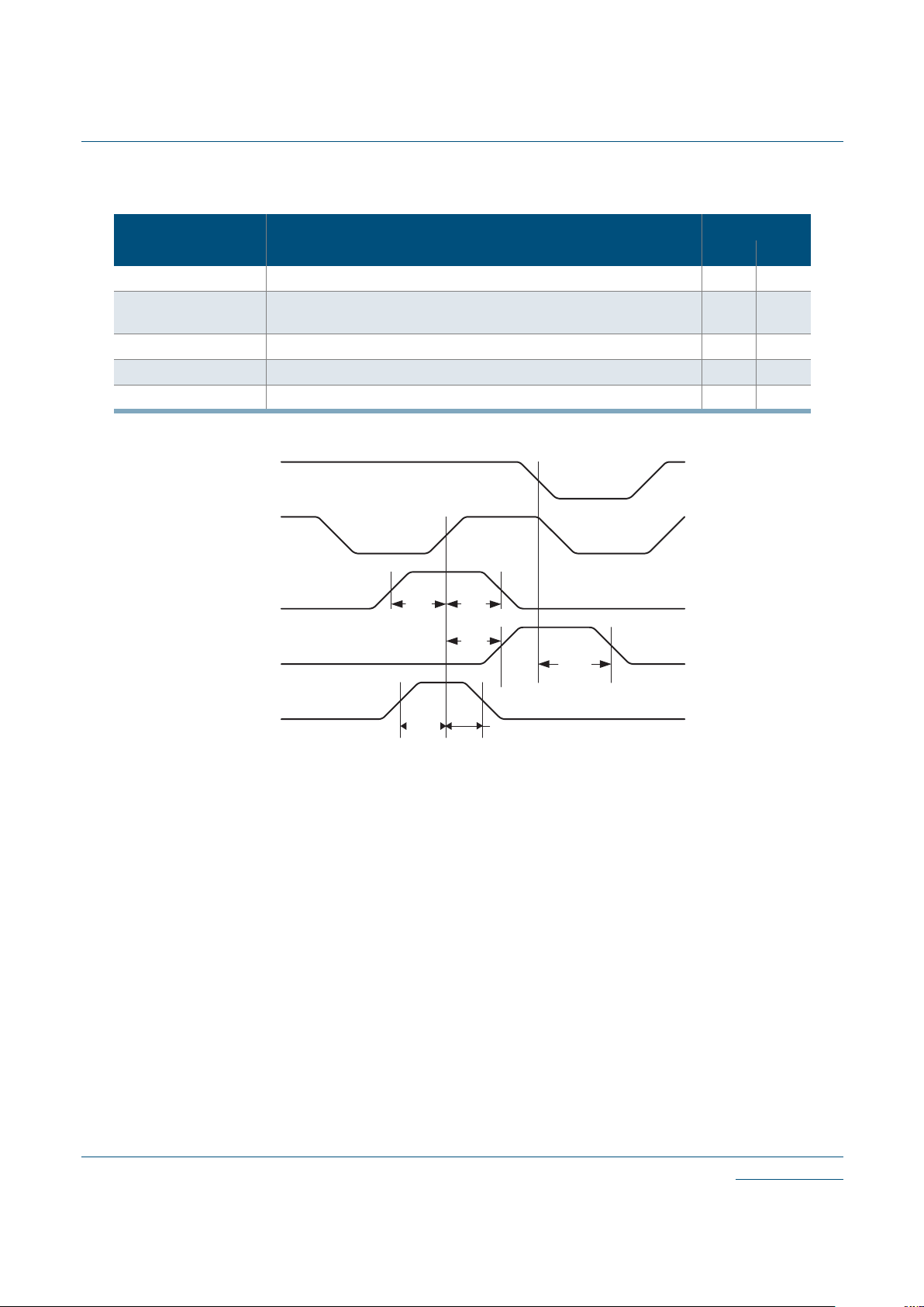
Figure 9: RAM Cell Synchronous Write Timing
Table 5: RAM Cell Synchronous & Asynchronous Read Timing
Symbol Parameter Value (ns)
RAM Cell Synchronous Read Timing Min Max
t
SRA
RA setup time to RCLK: time the READ ADDRESS must be stable before the active
edge of the READ CLOCK
0.686 -
t
HRA
RA hold time to RCLK: time the READ ADDRESS must be stable after the active
edge of the READ CLOCK
0 -
t
SRE
RE setup time to WCLK: time the READ ENABLE must be stable before the active
edge of the READ CLOCK
0.243 -
t
HRE
RE hold time to WCLK: time the READ ENABLE must be stable after the active
edge of the READ CLOCK
0 -
t
RCRD
RCLK to RD: time between the active READ CLOCK edge and the time when the
data is available at RD
- 4.38
RAM Cell Asynchronous Read Timing
r
PDRD
RA to RD: time between when the READ ADDRESS is input and when the DATA
is output
- 2.06
t
SWA
t
SWD
t
SWE
t
HWA
t
HWD
t
HWE
t
old data
new data
WCLK
WA
WD
WE
RD
© 2002 QuickLogic Corporati on
www.quicklogic.com
7
•
•
•
•
•
•
QL6325 Eclipse Data Sheet Rev C
Figure 10: RAM Cell Synchronous & Asynchronous Read Timing
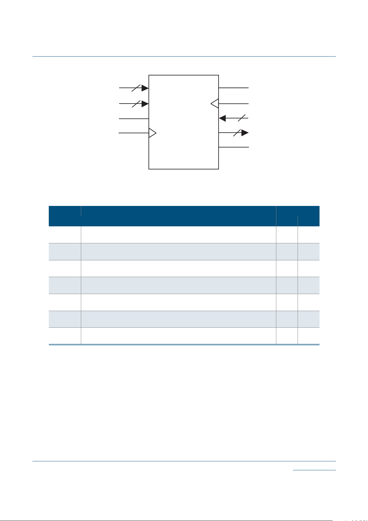
Figure 11: Eclipse Cell I/O
t
SRA
t
HRA
RCLK
RA
t
SRE
t
HRE
t
RCRD
old data
new data
RE
RD
r
PDRD
E
R
Q
D
R
Q
E
R
Q
D
+
-
PAD
OUTPUT ENABL E
REGISTER
OUTPUT
REGISTER
INPUT
REGISTER
D
8
www.quicklogic.com
© 2002 QuickLogic Corporation
•
•
•
•
•
•
QL6325 Eclipse Data Sheet Rev C
Figure 12: Eclipse Input Register Cell
Table 6: Input Register Cell
Symbol Parameter Value (ns)
Input Register Cell Only Min Max
t
ISU
Input register setup time: time the synchronous input of the flip-flop must be stable
before the active clock edge
3.12 -
t
IHL
Input register hold time: time the synchronous input of the flip-flop must be stable
after the active clock edge
0 -
t
ICO
Input register clock to out: time taken by the flip-flop to output after the active clock
edge
- 1.08
t
IRST
Input register reset delay: time between when the flip-flop is “reset”(low) and when
the output is consequently “reset” (low)
- 0.99
t
IESU
Input register clock enable setup time: time “enable” must be stable before the
active clock edge
0.37 -
t
IEH
Input register clock enable hold time: time “enable” must be stable after the active
clock edge
0 -
PAD
t
IN
, t
INI
t
ICLK
t
ISU
t
SID
+
-
Q
E
D
R
© 2002 QuickLogic Corporati on
www.quicklogic.com
9
•
•
•
•
•
•
QL6325 Eclipse Data Sheet Rev C
Figure 13: Eclipse Input Register Cell Timing
Table 7: Standard Input Delays
Symbol Parameter Value (ns)
Standard Input Delays To get the total input delay add this delay to tISU Min Max
t
SID
(LVTTL) LVTTL input delay: Low Voltage TTL for 3.3 V applications - 0.34
t
SID
(LVCMOS2)
LVCMOS2 input delay: Low Voltage CMOS for 2.5 V and lower
applications
- 0.42
t
SID
(GTL+) GTL+ input delay: Gunning Transceiver Logic - 0.68
t
SID
(SSTL3) SSTL3 input delay: Stub Series Terminated Logic for 3.3 V - 0.55
t
SID
(SSTL2) SSTL2 input delay: Stub Series Terminated Logic for 2.5 V - 0.61
R
CLK
D
Q
t
ISU
t
IHL
t
ICO
t
IESU
t
IEH
t
IRST
E
10
www.quicklogic.com
© 2002 QuickLogic Corporation
•
•
•
•
•
•
QL6325 Eclipse Data Sheet Rev C
Figure 14: Eclipse Output Register Cell
Table 8: Eclipse Output Register Cell
Symbol Parameter Value (ns)
Output Register Cell Only Min Max
t
OUTLH
Output Delay low to high (90% of H) - 0.40
t
OUTHL
Output Delay high to low (10% of L) - 0.55
t
PZH
Output Delay tri-state to high (90% of H) - 2.94
t
PZL
Output Delay tri-state to low (10% of L) - 2.34
t
PHZ
Output Delay high to tri-State - 3.07
t
PLZ
Output Delay low to tri-State - 2.53
t
COP
Clock to out delay (does not include clock tree delays) -
3.15 (fast slew)
10.2 (slow slew)
PAD
OUTPUT
REGISTER
© 2002 QuickLogic Corporati on
www.quicklogic.com
11
•
•
•
•
•
•
QL6325 Eclipse Data Sheet Rev C
Figure 15: Eclipse Output Register Cell Timing
Table 9: Output Slew Rates @ V
CCIO
= 3.3 V
Fast Slew Slow Slew
Rising Edge 2.8 V/ns 1.0 V/ns
Falling Edge 2.86 V/ns 1.0 V/ns
Table 10: Output Slew Rates @ V
CCIO
= 2.5 V
Fast Slew Slow Slew
Rising Edge 1.7 V/ns 0.6 V/ns
Falling Edge 1.9 V/ns 0.6 V/ns
L
H
L
H
t
OUTLH
t
OUTHL
L
H
Z
t
PZH
L
H
Z
t
PZL
L
H
Z
t
PLZ
L
H
Z
t
PHZ
12
www.quicklogic.com
© 2002 QuickLogic Corporation
•
•
•
•
•
•
QL6325 Eclipse Data Sheet Rev C
DC Characteristics
The DC Specifications are provided in Table 11 through Table 13.
Table 11: Absolute Maximum Ratings
Parameter Value Parameter Value
VCC Vol tage
-0.5 V to 3.6 V
DC Input Current
±20 mA
V
CCIO
Voltage
-0.5 V to 4.6 V
ESD Pad Protection
±2000 V
INREF Voltag e
2.7 V
Leaded Package
Storage Temperature
-65° C to + 150° C
Input Voltage
-0.5 V to V
CCIO
+0.5 V
Laminate Package (BGA)
Storage Temperature
-55° C to + 125° C
Latch-up Immunity
±100 mA
Table 12: Operating Range
Symbol Parameter Military Industrial Commercial Unit
Min Max Min Max Min Max
V
CC
Supply Voltage 2.3 2.7 2.3 2.7 2.3 2.7 V
V
CCIO
I/O Input Tolerance Voltage 2.3 3.6 2.3 3.6 2.3 3.6 V
TA Ambient Temperature -55 -40 85 0 70 °C
TC Case Temperature - 125 - - - - °C
K Delay Factor
-4 Speed Grade 0.42 2.3 0.43 2.16 0.47 2.11 n/a
-5 Speed Grade 0.42 1.92 0.43 1.80 0.46 1.76 n/a
-6 Speed Grade 0.42 1.35 0.43 1.26 0.46 1.23 n/a
-7 Speed Grade 0.42 1.27 0.43 1.19 0.46 1.16 n/a
Table 13: DC Characteristics
Symbol Parameter Conditions Min Max Units
I
I
I or I/O Input Leakage Current VI = V
CCIO
or GND -10 10 µA
I
OZ
3-State Output Leakage Current VI = V
CCIO
or GND -10 10 µA
C
I
Input Capacitance
a
a. Capacitance is sample tested only. Clock pins are 12 pF maximum.
--8pF
I
OS
Output Short Circuit Current
b
b. Only one output at a time. Duration should not exceed 30 seconds.
Vo = GND
V
o
= V
CC
-15
40
-180
210
mA
mA
I
CC
D.C. Supply Current
c
c. For -4/-5/-6/-7 commercial grade devices only. Maximum ICC is 3 mA for -0 commercial
grade and all industrial grade devices, and 5 mA for all military grade devices.
V
I,Vo
= V
CCIO
or GND 0.50 (typ) 2 mA
I
CCIO
D.C. Supply Current on V
CCIO
- 0 2 mA
I
CCIO
(DIF)
D.C. Supply Current on V
CCIO
for Differential I/O
---mA
I
REF
D.C. Supply Current on INREF - -10 10 µA
I
PD
Pad Pull-down (programmable) V
CCIO
= 3.6 V - 150 µA

© 2002 QuickLogic Corporati on
www.quicklogic.com
13
•
•
•
•
•
•
QL6325 Eclipse Data Sheet Rev C
I/O Characteristics
Figure 16: IOL vs. VOL
Figure 17: IOH vs. VOH
IOL vs VOL
0
20
40
60
80
100
120
140
160
180
0.00 0.20 0.40 0.60 0.80 1.00 1.20 1.40 1.60 1.80 2.00 2.20 2.40 2.60 2.80 3.00
Supply voltage (V)
Current (mA)
Vccio = 3.6V
Vccio = 3.3V
Vccio = 3.0V
Vccio = 2.7V
Vccio = 2.5V
Vccio = 2.3V
-120
-100
-80
-60
-40
-20
0
20
0.000.100.
30
0.500.700.901.101.301.501.
70
1.902.102.302.
50
2.702.903.003.
10
3.303.503.
60
Supply voltage (V)
Current (mA)
VccI/O = 2.3V
VccI/O = 2.5V
VccI/O = 2.7V
VccI/O = 3.3V
VccI/O = 3.6V
VccI/0 = 3.0V
IOH vs VOH

14
www.quicklogic.com
© 2002 QuickLogic Corporation
•
•
•
•
•
•
QL6325 Eclipse Data Sheet Rev C
NOTE:
The data provided in Table 14 are JEDEC and PCI Specifications. QuickLogic
®
devices
either meet or exceed these requirements. See preceding Table 1 through Table 13 and
Figure 1 through Figure 17 for data specific to QuickLogic I/Os.
NOTE:
All CLK and INREF pins are clamped to the VCC rail, not the V
CCIO
. Therefore, these pins
can only be driven up to V
CC
+ 0.3 V.
Table 14: DC Input and Output Leve ls
INREF V
IL
V
IH
V
OL
V
OH
I
OLIOH
V
MINVMAXVMIN
V
MAX
V
MIN
V
MAX
V
MAX
V
MIN
mA mA
LVTTL n/a n/a -0.3 0.8 2.0 V
CCIO
+ 0.3 0.4 2.4 2.0 -2.0
LVCMOS2 n/a n/a -0.3 0.7 1.7 V
CCIO
+ 0.3 0.7 1.7 2.0 -2.0
GTL+ 0.88 1.12 -0.3 INREF - 0.2 INREF + 0.2 V
CCIO
+ 0.3 0.6 n/a 40 n/a
PCI n/a n/a -0.3 0.3 x V
CCIO
0.5 x V
CCIO
V
CCIO
+ 0.5 0.1 x V
CCIO
0.9 x V
CCIO
1.5 -0.5
SSTL2 1.15 1.35 -0.3 INREF - 0.18 INREF + 0.18 V
CCIO
+ 0.3 0.74 1.76 7.6 -7.6
SSTL3 1.3 1.7 -0.3 INREF - 0.2 INREF + 0.2 V
CCIO
+ 0.3 1.10 1.90 8 -8

© 2002 QuickLogic Corporati on
www.quicklogic.com
15
•
•
•
•
•
•
QL6325 Eclipse Data Sheet Rev C
Package Thermal Characteristics
Thermal Resistance Equations:
θ
JC
= (TJ - TC)/P
θ
JA
= (TJ - TA)/P
P
MAX
= (T
JMAX
- T
AMAX
)/ θ
JA
Parameter Description:
θ
JC
: Junction-to-case thermal resistance
θ
JA
: Junction-to-ambient thermal resistance
TJ: Junction temperature
TA: Ambient temperature
P: Power dissipated by the device while operating
P
MAX
: The maximum power dissipation for the device
T
JMAX
: Maximum junction temperature
T
AMAX
: Maximum ambient temperature
NOTE:
Maximum junction temperature (T
JMAX
) is 150º C. To calculate the maximum power
dissipation for a device package look up
θ
JA
from Table 15, pick an appropriate T
AMAX
and
use:
P
MAX
= (150º C - T
AMAX
)/ θ
JA
Table 15: Package Thermal Characteristics
Package Description θJA (º C/W) @ various flow rates (m/sec) θ
JC
(º C/W)
Pin Count P ackage T ype 0 0.5 1 2
516 PBGA 20.0 19.0 17.5 16.0 7.0
484 PBGA 28.0 26.0 25.0 23.0 9.0
280 LF-PBGA 18.5 17.0 15.5 14.0 7.0
208 PQFP 26.0 24.5 23.0 22.0 11.0

16
www.quicklogic.com
© 2002 QuickLogic Corporation
•
•
•
•
•
•
QL6325 Eclipse Data Sheet Rev C
Kv and Kt Graphs
Figure 18: Voltage Factor vs. Supply Voltage
Figure 19: Temperature Factor vs. Operating Temperature
Voltage Factor vs. Supply Voltage
0.9200
0.9400
0.9600
0.9800
1.0000
1.0200
1.0400
1.0600
1.0800
1.1000
2.25 2.3 2.35 2.4 2.45 2.5 2.55 2.6 2.65 2.7 2.75
Supply Voltage (V)
Kv
Temperature Factor vs. Operating Temperature
0.85
0.90
0.95
1.00
1.05
1.10
1.15
-60 -40 -20 0 20 40 60 80
Junction Tempera ture C
Kt

© 2002 QuickLogic Corporati on
www.quicklogic.com
17
•
•
•
•
•
•
QL6325 Eclipse Data Sheet Rev C
Power vs. Operating Frequency
The basic power equation which best models power consumption is given below:
P
TOTAL
= 0.350 +
f
[0.0031 η
LC
+ 0.0948 η
CKBF
+ 0.01 η
CLBF
+ 0.0263 η
CKLD
+
0.543
η
RAM
+ 0.20 η
PLL
+ 0.0035 η
INP
+ 0.0257 η
OUTP
] (mW)
Where
• η
LC
is the total number of logic cells in the design
• η
CKBF
= # of clock buffers
• η
CLBF
= # of column clock buffers
• η
CKLD
= # of loads connected to the column clock buffers
• η
RAM
= # of RAM blocks
• η
PLL
= # of PLLs
• η
INP
is the number of input pins
• η
OUTP
is the number of output pins
Figure 20 exhibits the power consumption in an Eclipse QL6325 device. The chip was filled
with (300) 8-bit counters
approximately 76% logic cell utilization.
Figure 20: Power Consumption
Figure 21 illustrates the theoretical worst-case scenarios for 50%, 70%, and 90% utilizations
of the 6600-516 package. The resources of the device are divided exactly in half; meaning,
for 50% utilization, exactly 50% of the I/Os, Logic Cells, RAM blocks, clock network, etc
are utilized. These situations may never occur in a real design, but they do provide a very
rough quantitative measure of power consumption when talking in terms of 50% or 70%
utilization of an Eclipse device.
Power vs Freq. (Counter_300)
0
0.5
1
1.5
2
2.5
0 20 40 60 80 100 120 140
Frequency (Mhz)
Power (W)

18
www.quicklogic.com
© 2002 QuickLogic Corporation
•
•
•
•
•
•
QL6325 Eclipse Data Sheet Rev C
Figure 21: Power vs. Frequency (Absolute 50%, 70%, and 90% of the Available Resources on Chip)
To learn more about power consumption, please refer to application note #60 which is
located at
www.quicklogic.com.
Power vs. Frequency
0
1
2
3
4
5
6
7
0 50 100 150 200 250 300
Frequency (Mhz)
50% 70% 90%
Power (mW)

© 2002 QuickLogic Corporati on
www.quicklogic.com
19
•
•
•
•
•
•
QL6325 Eclipse Data Sheet Rev C
Power-up Sequencing
Figure 22: Power-up Requirements
The following requirements must be met when powering up a device (refer to Figure 22):
• When ramping up the power supplies keep (V
CCIO
-VCC)
MAX
≤ 500 mV. Deviation from
this recommendation can cause permanent damage to the device.
• V
CCIO
must lead VCC when ramping the device.
• The power supply must be greater than or equal to 400 µs to reach V
CC
. Ramping to
V
CC/VCCIO
before reaching 400 µs can cause the device to behave improperly.
A diode is present in-between VCC and V
CCIO
, as shown in Figure 23.
Figure 23: Internal Diode Between VCC and V
CCIO
Voltage
V
CCIO
V
CC
(V
CCIO
-VCC)
MAX
400 us
V
CC
V
CC
V
CCIO
Internal Logic
Cells, RAM
blocks, etc
IO Cells

20
www.quicklogic.com
© 2002 QuickLogic Corporation
•
•
•
•
•
•
QL6325 Eclipse Data Sheet Rev C
JTAG
Figure 24: JTAG Block Diagram
Microprocessors and Application Specific Integrated Circuits (ASICs) pose many design
challenges, not in the least of which concerns the accessibility of test points. The Joint Test
Access Group (JTAG) formed in response to this challenge, resulting in IEEE standard
1149.1, the Standard Test Access Port and Boundary Scan Architecture.
The JTAG boundary scan test methodology allows complete observation and control of the
boundary pins of a JTAG-compatible device through JTAG software. A Test Access Port
(TAP) controller works in concert with the Instruction Register (IR), which allow users to run
three required tests along with several user-defined tests.
JTAG tests allow users to reduce system debug time, reuse test platforms and tools, and reuse
subsystem tests for fuller verification of higher level system elements.
TCK
TMS
TRSTB
RDI
TDO
Instruction Decode
&
Control Logic
TAp Controller
State Machine
(16 States)
Instruction Register
Boundary-Scan Register
(Data Register)
Mux
Bypass
Register
Mux
Internal
Register
I/O Registers
User Defined Data Register

© 2002 QuickLogic Corporati on
www.quicklogic.com
21
•
•
•
•
•
•
QL6325 Eclipse Data Sheet Rev C
The 1149.1 standard requires the following three tests:
• Extest Instruction. The Extest instruction performs a PCB interconnect test. This test
places a device into an external boundary test mode, selecting the boundary scan
register to be connected between the TAP's Test Data In (TDI) and Test Data Out (TDO)
pins. Boundary scan cells are preloaded with test patterns (via the Sample/Preload
Instruction), and input boundary cells capture the input data for analysis.
• Sample/Preload Instruction. This instruction allows a device to remain in its
functional mode, while selecting the boundary scan register to be connected between
the TDI and TDO pins. For this test, the boundary scan register can be accessed via a
data scan operation, allowing users to sample the functional data entering and leaving
the device.
• Bypass Instruction. The Bypass instruction allows data to skip a device's boundary
scan entirely, so the data passes through the bypass register. The Bypass instruction
allows users to test a device without passing through other devices. The bypass register
is connected between the TDI and TDO pins, allowing serial data to be transferred
through a device without affecting the operation of the device.

22
www.quicklogic.com
© 2002 QuickLogic Corporation
•
•
•
•
•
•
QL6325 Eclipse Data Sheet Rev C
Pin Descriptions
Figure 25: I/O Banks with Relevant Pins
Table 16: JTAG Pin Descrip tions
Pin Function Description
TDI/RSI
Test Data In for JTAG/RAM
init. Serial Data In
Hold HIGH during normal operation. Connects to serial PROM
data in for RAM initialization. Connect to V
CC
if unused
TRSTB/RRO
Active low Reset for
JTAG/RAM init. reset out
Hold LOW during normal operation. Connects to serial PROM
reset for RAM initialization. Connect to GND if unused
TMS Test Mode Select for JTAG
Hold HIGH during normal operation. Connect to V
CC
if not used
for JTAG
TCK Test Clock for JTAG
Hold HIGH or LOW during normal operation. Connect to VCC or
ground if not used for JTAG
TDO/RCO
Test data out for JTAG/RAM
init. clock out
Connect to serial PROM clock for RAM initialization. Must be left
unconnected if not used for JTAG or RAM initialization
IO BANK A IO BANK B
V
CCIO
(A)
INREF(A)
IOCTRL(A)
IO(A)
V
CCIO
(A)
INREF(A)
IOCTRL(A)
IO(A)
IO BANK C IO BANK D
V
CCIO
(C)
INREF(C)
IOCTRL(C)
IO(C)
V
CCIO
(D)
INREF(D)
IOCTRL(D)
IO(D)
IO BANK F IO BANK E
V
CCIO
(F)
INREF(F)
IOCTRL(F)
IO(F)
V
CCIO
(E)
INREF(E)
IOCTRL(E)
IO(E)
IO BANK HIO BANK G
(H)
INREF(H)
IOCTRL(H)
IO(H)
V
CCIO
V
CCIO
(G)
INREF(G)
IOCTRL(G)
IO(G)

© 2002 QuickLogic Corporati on
www.quicklogic.com
23
•
•
•
•
•
•
QL6325 Eclipse Data Sheet Rev C
Table 17: Dedicat ed Pin Descriptions
Pin Function Description
CLK
High-drive input and/or global
clock network driver
Can be configured as either input or global clock
I/O(A) Input/Output pin
The I/O pin is a bi-directional pin, configurable to either an inputonly, output-only, or bi-directional pin. The A inside the
parenthesis means that the I/O is located in Bank A. If an I/O is
not used, SpDE (QuickWorks Tool) provides the option of tying
that pin to GND, V
CC,
or TriState during programming.
V
CC
Power supply pin Connect to 2.5 V supply
V
CCIO
(A) Input voltage tolerance pin
This pin provides the flexibility to interface the device with either a
3.3 V device or a 2.5 V device. The A inside the parenthesis
means that V
CCIO
is located in BANK A. Every I/O pin in Bank A
will be tolerant of V
CCIO
input signals and will output V
CCIO
level
signals. This pin must be connected to either 3.3 V or V
CC
.
GND Ground pin Connect to ground
PLLIN PLL clock input Clock input for PLL
DEDCLK Dedicated clock pin Low skew global clock
GNDPLL Ground pin for PLL Connect to GND
INREF(A) Differential reference voltage
The INREF is the reference voltage pin for GTL+, SSTL2, and
STTL3 standards. Follow the recommendations provided in
Table 14 for the appropriate standard. The A inside the
parenthesis means that INREF is located in BANK A. This pin
should be tied to GND if not needed.
PLLOUT PLL output pin Dedicated PLL output pin; otherwise, may be left unconnected
IOCTRL(A) Highdrive input
This pin provides fast RESET, SET, CLOCK, and ENABLE access
to the I/O cell flip-flops, providing fast clock-to-out and fast I/O
response times. This pin can also double as a high-drive pin to the
internal logic cells. The A inside the parenthesis means that
IOCTRL is located in Bank A. This pin should be tied to GND or
V
CC
if it is not used.

24
www.quicklogic.com
© 2002 QuickLogic Corporation
•
•
•
•
•
•
QL6325 Eclipse Data Sheet Rev C
Recommended Unused Pin Terminations for the Eclipse devices
All unused, general purpose I/O pins can be tied to VCC, GND, or HIZ (high impedance)
internally using the Configuration Editor. This option is given in the bottom-right corner of
the placement window. To use the Placement Editor, choose Constraint
ÆFix Placement
in the Option pull-down menu of SpDE.
The rest of the pins should be terminated at the board level in the manner presented in
Table 18.
NOTE:
x -> number, y -> alphabetical character.
Ordering Information
Figure 26: Ordering Information
Table 18: Recommended Unused Pin Terminations
Signal Name Recommended Termination
PLLOUT<x>
Unused PLL output pins must be connected to either VCC or GND so that their associated
input buffer never floats. Utilized PLL output pins that route the PLL clock outside of the
chip should not be tied to either VCC or GND.
IOCTRL<y> Any unused pins of this type must be connected to either VCC or GND.
CLK/PLLIN<x> Any unused clock pins should be connected to VCC or GND.
PLLRST<x>
If a PLL module is not used, then the associated PLLRST<x> must be connected to VCC,
under normal operation use it as needed.
INREF<y>
If an I/O bank does not require the use of INREF signal the pin should be connected to
GND.
QL 6325 - 4 PB516 C
QuickLogic device
Eclipse device
part number
Speed Grade
4 = Quick
5 = Fast
6 = Faster
7 = Fastest
Operating Range
C = Commercial
I = Industrial
M = Military
Package Code
PT208 = 208-pin FPBGA
PT280 = 280-pin FPBGA
PS484 = 484-pin BGA (1.0 mm)
PB516 = 516-pin BGA (1.27 mm)

© 2002 QuickLogic Corporati on
www.quicklogic.com
25
•
•
•
•
•
•
QL6325 Eclipse Data Sheet Rev C
208 PQFP Pinout Diagram
Eclipse
QL6325-4PQ208C

26
www.quicklogic.com
© 2002 QuickLogic Corporation
•
•
•
•
•
•
QL6325 Eclipse Data Sheet Rev C
208 PQFP Pinout Table
Table 19: 208 PQFP Pinout Table
208 PQFP Function 208 PQFP Function 208 PQFP Function 208 PQFP Function 208 PQFP Function
1
PLLRST(3)
43
IO(B)
85
IO(D)
127
CLK(5),PLLIN(3)
169
IOCTRL(G)
2
V
CCPLL
(3)
44
V
CCIO
(B)
86
V
CC
128
CLK(6)
170
INREF(G)
3
GND
45
IO(B)
87
IO(D)
129
V
CC
171
IOCTRL(G)
4
GND
46
V
CC
88
IO(D)
130
CLK(7)
172
IO(G)
5
IO(A)
47
IO(B)
89
V
CC
131
V
CC
173
IO(G)
6
IO(A)
48
IO(B)
90
IO(D)
132
CLK(8)
174
IO(V)
7
IO(A)
49
GND
91
IO(D)
133
TMS
175
V
CC
8
V
CCIO
(A)
50
TDO
92
IOCTRL(D)
134
IO(F)
176
IO(G)
9
IO(A)
51
PLLOUT(1)
93
INREF(D)
135
IO(F)
177
V
CCIO
(G)
10
IO(A)
52
GNDPLL(2)
94
IOCTRL(D)
136
IO(F)
178
GND
11
IOCTRL(A)
53
GND
95
IO(D)
137
GND
179
IO(G)
12
V
CC
54
V
CCPLL
(2)
96
IO(D)
138
V
CCIO
(F)
180
IO(G)
13
INREF(A)
55
PLLRST(2)
97
IO(D)
139
IO(F)
181
IO(G)
14
IOCTRL(A)
56
V
CC
98
V
CCIO
(D)
140
IO(F)
182
V
CC
15
IO(A)
57
IO(C)
99
IO(D)
141
IO(F)
183
TCK
16
IO(A)
58
GND
100
IO(D)
142
IO(F)
184
V
CC
17
IO(A)
59
IO(C)
101
GND
143
IO(F)
185
IO(H)
18
IO(A)
60
V
CCIO
(C)
102
PLLOUT(0)
144
IOCTRL(F)
186
IO(H)
19
V
CCIO
(A)
61
IO(C)
103
GND
145
INREF(F)
187
IO(H)
20
IO(A)
62
IO(C)
104
GNDPLL(1)
146
V
CC
188
GND
21
GND
63
IO(C)
105
PLLRST(1)
147
IOCTRL(F)
189
V
CCIO
(H)
22
IO(A)
64
IO(C)
106
V
CCPLL
(1)
148
IO(F)
190
IO(H)
23
TDI
65
IO(C)
107
IO(E)
149
IO(F)
191
IO(H)
24
CLK(0)
66
IO(C)
108
GND
150
V
CCIO
(F)
192
IOCTRL(H)
25
CLK(1)
67
IOCTRL(C)
109
IO(E)
151
IO(F)
193
IO(H)
26
V
CC
68
INREF(C)
110
IO(E)
152
IO(F)
194
INREF(H)
27
CLK(2),PLLIN(2)
69
IOCTRL(C)
111
V
CCIO
(E)
153
GND
195
V
CC
28
CLK(3),PLLIN(1)
70
IO(C)
112
IO(E)
154
IO(F)
196
IOCTRL(H)
29
V
CC
71
IO(C)
113
V
CC
155
PLLOUT(3)
197
IO(H)
30
CLK(4),
DEDCLK,PLLIN(0)
72
V
CCIO
(C)
114
IO(E)
156
GNDPLL(0)
198
IO(H)
31
IO(B)
73
IO(C)
115
IO(E)
157
GND
199
IO(H)
32
IO(B)
74
IO(C)
116
IO(E)
158
V
CCPLL
(0)
200
IO(H)
33
GND
75
GND
117
IOCTRL(E)
159
PLLRST(0)
201
IO(H)
34
V
CCIO
(B)
76
V
CC
118
INREF(E)
160
GND
202
IO(H)
35
IO(B)
77
IO(C)
119
IOCTRL(E)
161
IO(G)
203
V
CCIO
(H)
36
IO(B)
78
TRSTB
120
IO(E)
162
V
CCIO
(G)
204
GND
37
IO(B)
79
V
CC
121
IO(E)
163
IO(G)
205
IO(H)
38
IO(B)
80
IO(D)
122
V
CCIO
(E)
164
IO(G)
206
PLLOUT(2)
39
IOCTRL(B)
81
IO(D)
123
GND
165
V
CC
207
GND
40
INREF(B)
82
IO(D)
124
IO(E)
166
IO(G)
208
GNDPLL(3)
41
IOCTRL(B)
83
GND
125
IO(E)
167
IO(G)
42
IO(B)
84
V
CCIO
(D)
126
IO(E)
168
IO(G)

© 2002 QuickLogic Corporati on
www.quicklogic.com
27
•
•
•
•
•
•
QL6325 Eclipse Data Sheet Rev C
280 PBGA Pinout Diagram
Top
Bottom
Eclipse
QL6325-4PT280C
Pin A1
Corner
28
www.quicklogic.com
© 2002 QuickLogic Corporation
•
•
•
•
•
•
QL6325 Eclipse Data Sheet Rev C
280 PBGA Pinout Table
Table 20: 280 PBGA Pinout Table
280 PBGA Function 280 PBGA Function 280 PBGA Function 280 PBGA Function 2 80 PBG A Function 280 PBGA Function
A1
PLLOUT<3>
C10
CLK<5>
/PLLIN<3>
E19
IOCTRL<D>
K16
I/O<C>
R4
I/O<H>
U13
I/O<B>
A2
GNDPLL<0>
C11
V
CCIO
<E>
F1
INREF<G>
K17
I/O<D>
R5
GND
U14
IOCTRL<B>
A3
I/O<F>
C12
I/O<E>
F2
IOCTRL<G>
K18
I/O<C>
R6
GND
U15
V
CCIO
<B>
A4
I/O<F>
C13
I/O<E>
F3
I/O<G>
K19
TRSTB
R7
V
CC
U16
I/O<B>
A5
I/O<F>
C14
I/O<E>
F4
I/O<G>
L1
I/O<H>
R8
V
CC
U17
TDO
A6
IOCTRL<F>
C15
V
CCIO
<E>
F5
GND
L2
I/O<H>
R9
GND
U18
PLLRST<2>
A7
I/O<F>
C16
I/O<E>
F15
V
CC
L3
V
CCIO
<H>
R10
GND
U19
I/O<B>
A8
I/O<F>
C17
I/O<E>
F16
IOCTRL<D>
L4
I/O<H>
R11
V
CC
V1
PLLOUT<2>
A9
I/O<F>
C18
I/O<E>
F17
I/O<D>
L5
V
CC
R12
V
CC
V2
GNDPLL<3>
A10
CLK<7>
C19
I/O<E>
F18
I/O<D>
L15
GND
R13
V
CC
V3
GND
A11
I/O<E>
D1
I/O<G>
F19
I/O<D>
L16
I/O<C>
R14
V
CC
V4
I/O<A>
A12
I/O<E>
D2
I/O<G>
G1
I/O<G>
L17
V
CCIO
<C>
R15
GND
V5
I/O<A>
A13
I/O<E>
D3
I/O<F>
G2
I/O<G>
L18
I/O<C>
R16
I/O<C>
V6
IOCTRL<A>
A14
IOCTRL<E>
D4
I/O<F>
G3
IOCTRL<G>
L19
I/O<C>
R17
V
CCIO
<C>
V7
I/O<A>
A15
I/O<E>
D5
I/O<F>
G4
I/O<G>
M1
I/O<H>
R18
I/O<C>
V8
I/O<A>
A16
I/O<E>
D6
I/O<F>
G5
V
CC
M2
I/O<H>
R19
I/O<C>
V9
I/O<A>
A17
I/O<E>
D7
I/O<F>
G15
V
CC
M3
I/O<H>
T1
I/O<H>
V10
CLK<1>
A18
PLLRST<1>
D8
I/O<F>
G16
I/O<D>
M4
I/O<H>
T2
I/O<H>
V11
CLK<4>
DEDCLK/PLLIN<0>
A19
GND
D9
CLK<8>
G17
I/O<D>
M5
V
CC
T3
I/O<A>
V12
I/O<B>
B1
PLLRST<0>
D10
I/O<E>
G18
I/O<D>
M15
V
CC
T4
I/O<A>
V13
I/O<B>
B2
GND
D11
I/O<E>
G19
I/O<D>
M16
INREF<C>
T5
I/O<A>
V14
INREF<B>
B3
I/O<F>
D12
I/O<E>
H1
I/O<G>
M17
I/O<C>
T6
IOCTRL<A>
V15
I/O<B>
B4
I/O<F>
D13
INREF<E>
H2
I/O<G>
M18
I/O<C>
T7
I/O<A>
V16
I/O<B>
B5
I/O<F>
D14
I/O<E>
H3
I/O<G>
M19
I/O<C>
T8
I/O<A>
V17
I/O<B>
B6
INREF<F>
D15
I/O<E>
H4
I/O<G>
N1
IOCTRL<H>
T9
I/O<A>
V18
GNDPLL<2>
B7
I/O<F>
D16
I/O<D>
H5
V
CC
N2
I/O<H>
T10
I/O<A>
V19
GND
B8
I/O<F>
D17
I/O<D>
H15
V
CC
N3
I/O<H>
T11
CLK<3>
/PLLIN<1>
W1
GND
B9
TMS
D18
I/O<D>
H16
V
CC
N4
I/O<H>
T12
I/O<B>
W2
PLLRST<3>
B10
CLK<6>
D19
I/O<D>
H17
I/O<D>
N5
V
CC
T13
I/O<B>
W3
I/O<A>
B11
I/O<E>
E1
I/O<G>
H18
I/O<D>
N15
V
CC
T14
I/O<B>
W4
I/O<A>
B12
I/O<E>
E2
I/O<G>
H19
I/O<D>
N16
I/O<C>
T15
I/O<B>
W5
I/O<A>
B13
IOCTRL<E>
E3
V
CCIO
<G>
J1
I/O<G>
N17
I/O<C>
T16
I/O<B>
W6
I/O<A>
B14
I/O<E>
E4
I/O<F>
J2
I/O<G>
N18
IOCTRL<C>
T17
V
CCPLL
<2>
W7
I/O<A>
B15
I/O<E>
E5
GND
J3
V
CCIO
<G>
N19
IOCTRL<C>
T18
I/O<B>
W8
I/O<A>
B16
I/O<E>
E6
V
CC
J4
I/O<G>
P1
I/O<H>
T19
I/O<B>
W9
TDI
B17
V
CCPLL
<1>
E7
V
CC
J5
GND
P2
I/O<H>
U1
I/O<A>
W10
CLK<2>
/PLLIN<2>
B18
GNDPLL<1>
E8
V
CC
J15
V
CC
P3
IOCTRL<H>
U2
I/O<A>
W11
I/O<B>
B19
PLLOUT<0>
E9
V
CC
J16
I/O<C>
P4
INREF<H>
U3
V
CCPLL
<3>
W12
I/O<B>
C1
I/O<F>
E10
GND
J17
V
CCIO
<D>
P5
V
CC
U4
I/O<A>
W13
I/O<B>
C2
V
CCPLL
<0>
E11
GND
J18
I/O<D>
P15
GND
U5
V
CCIO
<A>
W14
IOCTRL<B>
C3
I/O<F>
E12
V
CC
J19
I/O<D>
P16
I/O<C>
U6
INREF<A>
W15
I/O<B>
C4
I/O<F>
E13
V
CC
K1
V
CC
P17
I/O<C>
U7
I/O<A>
W16
I/O<B>
C5
V
CCIO
<F>
E14
GND
K2
TCK
P18
I/O<C>
U8
I/O<A>
W17
I/O<B>
C6
IOCTRL<F>
E15
GND
K3
I/O<G>
P19
I/O<C>
U9
V
CCIO
<A>
W18
I/O<B>
C7
I/O<F>
E16
I/O<D>
K4
I/O<G>
R1
I/O<H>
U10
CLK<0>
W19
PLLOUT<1>
C8
I/O<F>
E17
V
CCIO
<D>
K5
GND
R2
I/O<H>
U11
V
CCIO
<B>
C9
V
CCIO
<F>
E18
INREF<D>
K15
GND
R3
V
CCIO
<H>
U12
I/O<B>

© 2002 QuickLogic Corporati on
www.quicklogic.com
29
•
•
•
•
•
•
QL6325 Eclipse Data Sheet Rev C
280 PBGA Packaging Drawing
Figure 27: 280 PBGA Packaging Drawing

30
www.quicklogic.com
© 2002 QuickLogic Corporation
•
•
•
•
•
•
QL6325 Eclipse Data Sheet Rev C
484 PBGA Pinout Diagram
Top
Bottom
Eclipse
QL6325-4PS484C
20 19 18 17 16 15 14 13 12 11 10 9 8 7 6 5 4 3 2 1
A
B
C
E
D
F
G
H
K
J
L
M
N
R
P
T
U
V
Y
W
22 21
AB
AA
Pin A1
Corner
Pin A1

© 2002 QuickLogic Corporati on
www.quicklogic.com
31
•
•
•
•
•
•
QL6325 Eclipse Data Sheet Rev C
484 PBGA Pinout Table
Table 21: 484 PBGA Pinout Table
484 PBGA Function 484 PBGA Function 484 PBGA Function 484 PBGA Function 484 PBGA Function 484 PBGA Function
A1
I/O<A>
C1
I/O<A>
E1
IOCTRL<A>
G1
I/O<A>
J1
I/O<A>
L1
CLK<4>
DEDCLK/PLLIN<0>
A2
PLLRST<3>
C2
I/O<A>
E2
I/O<A>
G2
I/O<A>
J2
I/O<A>
L2
CLK<0>
A3
I/O<A>
C3
V
CCPLL
<3>
E3
I/O<A>
G3
I/O<A>
J3
I/O<A>
L3
CLK<2>/PLLIN<2>
A4
I/O<A>
C4
PLLOUT<2>
E4
I/O<A>
G4
I/O<A>
J4
I/O<A>
L4
I/O<A>
A5
I/O<A>
C5
I/O<A>
E5
I/O<A>
G5
I/O<A>
J5
I/O<A>
L5
I/O<A>
A6
I/O<H>
C6
I/O<H>
E6
I/O<H>
G6
I/O<A>
J6
I/O<A>
L6
I/O<A>
A7
I/O<H>
C7
I/O<H>
E7
N/C
G7
GND
J7
I/O<A>
L7
GND
A8
IOCTRL<H>
C8
I/O<H>
E8
I/O<H>
G8
I/O<H>
J8
V
CC
L8
GND
A9
I/O<H>
C9
IOCTRL<H>
E9
I/O<H>
G9
I/O<H>
J9
GND
L9
GND
A10
N/C
C10
I/O<H>
E10
I/O<H>
G10
I/O<H>
J10
V
CC
L10
GND
A11
N/C
C11
I/O<H>
E11
V
CC
G11
I/O<G>
J11
V
CC
L11
GND
A12
TCK
C12
I/O<H>
E12
I/O<G>
G12
GND
J12
GND
L12
GND
A13
I/O<G>
C13
I/O<G>
E13
I/O<G>
G13
I/O<G>
J13
V
CC
L13
GND
A14
I/O<G>
C14
I/O<G>
E14
I/O<G>
G14
I/O<G>
J14
GND
L14
V
CC
A15
I/O<G>
C15
I/O<G>
E15
IOCTRL<G>
G15
I/O<G>
J15
V
CC
L15
V
CC
A16
I/O<G>
C16
I/O<G>
E16
I/O<G>
G16
GND
J16
I/O<F>
L16
CLK<6>
A17
I/O<G>
C17
I/O<G>
E17
INREF<G>
G17
V
CCIO
<F>
J17
V
CCIO
<F>
L17
V
CCIO
<F>
A18
I/O<G>
C18
I/O<G>
E18
I/O<G>
G18
I/O<F>
J18
I/O<F>
L18
I/O<F>
A19
I/O<F>
C19
I/O<F>
E19
I/O<F>
G19
I/O<F>
J19
I/O<F>
L19
CLK<8>
A20
GND
C20
GNDPLL<0>
E20
I/O<F>
G20
I/O<F>
J20
I/O<F>
L20
I/O<F>
A21
PLLOUT<3>
C21
I/O<F>
E21
I/O<F>
G21
INREF<F>
J21
I/O<F>
L21
I/O<F>
A22
I/O<F>
C22
I/O<F>
E22
I/O<F>
G22
I/O<F>
J22
I/O<F>
L22
I/O<F>
B1
I/O<A>
D1
I/O<A>
F1
I/O<A>
H1
I/O<A>
K1
TDI
M1
I/O<B>
B2
GND
D2
I/O<A>
F2
INREF<A>
H2
I/O<A>
K2
I/O<A>
M2
I/O<B>
B3
GNDPLL<3>
D3
I/O<A>
F3
I/O<A>
H3
I/O<A>
K3
I/O<A>
M3
I/O<B>
B4
GND
D4
I/O<A>
F4
I/O<A>
H4
I/O<A>
K4
I/O<A>
M4
CLK<3>/PLLIN<1>
B5
I/O<A>
D5
I/O<A>
F5
I/O<A>
H5
IOCTRL<A>
K5
I/O<A>
M5
I/O<B>
B6
I/O<H>
D6
I/O<H>
F6
V
CCIO
<A>
H6
V
CCIO
<A>
K6
V
CCIO
<A>
M6
V
CCIO
<B>
B7
I/O<H>
D7
I/O<H>
F7
V
CCIO
<H>
H7
I/O<H>
K7
I/O<A>
M7
CLK<1>
B8
INREF<H>
D8
I/O<H>
F8
I/O<H>
H8
GND
K8
V
CC
M8
V
CC
B9
I/O<H>
D9
I/O<H>
F9
V
CCIO
<H>
H9
V
CC
K9
V
CC
M9
V
CC
B10
I/O<H>
D10
I/O<H>
F10
I/O<H>
H10
V
CC
K10
GND
M10
GND
B11
I/O<H>
D11
I/O<H>
F11
V
CCIO
<H>
H11
V
CC
K11
GND
M11
GND
B12
N/C
D12
I/O<G>
F12
V
CCIO
<G>
H12
GND
K12
GND
M12
GND
B13
N/C
D13
I/O<G>
F13
I/O<G>
H13
V
CC
K13
GND
M13
GND
B14
N/C
D14
I/O<G>
F14
V
CCIO
<G>
H14
V
CC
K14
V
CC
M14
GND
B15
I/O<G>
D15
IOCTRL<G>
F15
N/C
H15
GND
K15
V
CC
M15
GND
B16
I/O<G>
D16
I/O<G>
F16
V
CCIO
<G>
H16
I/O<F>
K16
I/O<F>
M16
GND
B17
I/O<G>
D17
I/O<G>
F17
N/C
H17
I/O<F>
K17
I/O<F>
M17
I/O<E>
B18
I/O<G>
D18
I/O<F>
F18
I/O<F>
H18
I/O<F>
K18
I/O<F>
M18
I/O<E>
B19
PLLRST<0>
D19
V
CCPLL
<0>
F19
I/O<F>
H19
I/O<F>
K19
I/O<F>
M19
I/O<E>
B20
I/O<F>
D20
I/O<F>
F20
IOCTRL<F>
H20
I/O<F>
K20
I/O<F>
M20
CLK<7>
B21
I/O<F>
D21
I/O<F>
F21
I/O<F>
H21
I/O<F>
K21
I/O<F>
M21
CLK<5>/PLLIN<3>
B22
I/O<F>
D22
I/O<F>
F22
IOCTRL<F>
H22
I/O<F>
K22
I/O<F>
M22
TMS
(Sheet 1 of 2)

32
www.quicklogic.com
© 2002 QuickLogic Corporation
•
•
•
•
•
•
QL6325 Eclipse Data Sheet Rev C
N1
I/O<B>
P16
I/O<E>
T9
N/C
V2
I/O<B>
W17
I/O<D>
AA10
I/O<C>
N2
I/O<B>
P17
I/O<E>
T10
TRSTB
V3
I/O<B>
W18
I/O<E>
AA11
I/O<C>
N3
I/O<B>
P18
I/O<E>
T11
GND
V4
I/O<B>
W19
I/O<E>
AA12
I/O<D>
N4
I/O<B>
P19
I/O<E>
T12
N/C
V5
I/O<B>
W20
I/O<E>
AA13
I/O<D>
N5
I/O<B>
P20
I/O<E>
T13
I/O<D>
V6
I/O<C>
W21
I/O<E>
AA14
I/O<D>
N6
I/O<B>
P21
I/O<E>
T14
N/C
V7
I/O<C>
W22
I/O<E>
AA15
I/O<D>
N7
I/O<B>
P22
I/O<E>
T15
I/O<D>
V8
I/O<C>
Y1
I/O<B>
AA16
I/O<D>
N8
V
CC
R1
I/O<B>
T16
GND
V9
N/C
Y2
I/O<B>
AA17
I/O<D>
N9
V
CC
R2
INREF<B>
T17
I/O<E>
V10
I/O<C>
Y3
V
CCPLL
<2>
AA18
I/O<D>
N10
GND
R3
I/O<B>
T18
I/O<E>
V11
I/O<C>
Y4
I/O<C>
AA19
I/O<E>
N11
GND
R4
I/O<B>
T19
I/O<E>
V12
V
CC
Y5
I/O<C>
AA20
GNDPLL<1>
N12
GND
R5
I/O<B>
T20
I/O<E>
V13
N/C
Y6
I/O<C>
AA21
I/O<E>
N13
GND
R6
I/O<B>
T21
IOCTRL<E>
V14
I/O<D>
Y7
I/O<C>
AA22
I/O<E>
N14
V
CC
R7
I/O<B>
T22
I/O<E>
V15
I/O<D>
Y8
IOCTRL<C>
AB1
I/O<B>
N15
V
CC
R8
GND
U1
IOCTRL<B>
V16
INREF<D>
Y9
I/O<C>
AB2
GNDPLL<2>
N16
I/O<E>
R9
V
CC
U2
I/O<B>
V17
I/O<D>
Y10
I/O<C>
AB3
PLLRST<2>
N17
V
CCIO
<E>
R10
V
CC
U3
IOCTRL<B>
V18
I/O<E>
Y11
I/O<D>
AB4
I/O<B>
N18
I/O<E>
R11
GND
U4
I/O<B>
V19
I/O<E>
Y12
I/O<D>
AB5
I/O<B>
N19
I/O<E>
R12
V
CC
U5
I/O<B>
V20
I/O<E>
Y13
I/O<D>
AB6
I/O<C>
N20
I/O<E>
R13
V
CC
U6
I/O<C>
V21
I/O<E>
Y14
I/O<D>
AB7
I/O<C>
N21
I/O<E>
R14
V
CC
U7
V
CCIO
<C>
V22
I/O<E>
Y15
IOCTRL<D>
AB8
IOCTRL<C>
N22
I/O<E>
R15
GND
U8
N/C
W1
I/O<B>
Y16
I/O<D>
AB9
I/O<C>
P1
I/O<B>
R16
I/O<D>
U9
V
CCIO
<C>
W2
I/O<B>
Y17
I/O<D>
AB10
I/O<C>
P2
I/O<B>
R17
V
CCIO
<E>
U10
I/O<C>
W3
I/O<B>
Y18
I/O<E>
AB11
I/O<C>
P3
I/O<B>
R18
I/O<E>
U11
V
CCIO
<C>
W4
I/O<B>
Y19
PLLOUT<0>
AB12
I/O<D>
P4
I/O<B>
R19
I/O<E>
U12
V
CCIO
<D>
W5
I/O<B>
Y20
PLLRST<1>
AB13
I/O<D>
P5
I/O<B>
R20
I/O<E>
U13
I/O<D>
W6
I/O<C>
Y21
I/O<E>
AB14
I/O<D>
P6
V
CCIO
<B>
R21
I/O<E>
U14
V
CCIO
<D>
W7
N/C
Y22
I/O<E>
AB15
I/O<D>
P7
I/O<B>
R22
I/O<E>
U15
N/C
W8
I/O<C>
AA1
TDO
AB16
IOCTRL<D>
P8
V
CC
T1
I/O<B>
U16
V
CCIO
<D>
W9
I/O<C>
AA2
PLLOUT<1>
AB17
I/O<D>
P9
GND
T2
I/O<B>
U17
V
CCIO
<E>
W10
I/O<C>
AA3
GND
AB18
I/O<D>
P10
V
CC
T3
I/O<B>
U18
I/O<E>
W11
I/O<C>
AA4
I/O<B>
AB19
I/O<E>
P11
GND
T4
I/O<B>
U19
I/O<E>
W12
I/O<D>
AA5
I/O<C>
AB20
GND
P12
V
CC
T5
I/O<B>
U20
IOCTRL<E>
W13
I/O<D>
AA6
I/O<C>
AB21
V
CCPLL
<1>
P13
V
CC
T6
V
CCIO
<B>
U21
I/O<E>
W14
I/O<D>
AA7
I/O<C>
AB22
I/O<E>
P14
GND
T7
GND
U22
INREF<E>
W15
I/O<D>
AA8
INREF<C>
P15
V
CC
T8
I/O<C>
V1
I/O<B>
W16
N/C
AA9
I/O<C>
Table 21: 484 PBGA Pinout Table (Continued)
484 PBGA Function 484 PBGA Function 484 PBGA Function 484 PBGA Function 484 PBGA Function 484 PBGA Function
(Sheet 2 of 2)

© 2002 QuickLogic Corporati on
www.quicklogic.com
33
•
•
•
•
•
•
QL6325 Eclipse Data Sheet Rev C
484 PBGA Packaging Drawing
Figure 28: 484 PBGA Packaging Drawing

34
www.quicklogic.com
© 2002 QuickLogic Corporation
•
•
•
•
•
•
QL6325 Eclipse Data Sheet Rev C
516 PBGA Pinout Diagram
Top
Bottom
Eclipse
QL6325-4PB516C
PIN A1
CORNER
© 2002 QuickLogic Corporati on
www.quicklogic.com
35
•
•
•
•
•
•
QL6325 Eclipse Data Sheet Rev C
516 PBGA Pinout Table
Table 22: 516 PBGA Pinout Table
516 PBGA Function 516 PBGA Function 516 PBGA Function 516 PBGA Function 516 PBGA Function 516 PBGA Function
A1
GND
C1
I/O<F>
E1
I/O<G>
G1
I/O<G>
L5
V
CC
P3
I/O<H>
A2
I/O<F>
C2
N/C
E2
I/O<G>
G2
INREF<G>
L6
V
CC
P4
V
CC
A3
I/O<F>
C3
I/O<F>
E3
N/C
G3
I/O<G>
L11
GND
P5
I/O<H>
A4
I/O<F>
C4
PLLOUT<3>
E4
V
CCPLL
<0>
G4
I/O<G>
L12
GND
P6
V
CCIO
<H>
A5
I/O<F>
C5
I/O<F>
E5
I/O<F>
G5
I/O<G>
L13
GND
P11
GND
A6
I/O<F>
C6
I/O<F>
E6
I/O<F>
G6
V
CCIO
<G>
L14
GND
P12
GND
A7
IOCTRL<F>
C7
I/O<F>
E7
I/O<F>
G21
V
CCIO
<D>
L15
GND
P13
GND
A8
I/O<F>
C8
INREF<F>
E8
V
CC
G22
I/O<D>
L16
GND
P14
GND
A9
I/O<F>
C9
I/O<F>
E9
I/O<F>
G23
I/O<D>
L21
V
CC
P15
GND
A10
I/O<F>
C10
I/O<F>
E10
I/O<F>
G24
I/O<D>
L22
I/O<D>
P16
GND
A11
I/O<F>
C11
I/O<F>
E11
I/O<F>
G25
I/O<D>
L23
I/O<D>
P21
V
CCIO
<C>
A12
I/O<F>
C12
I/O<F>
E12
V
CC
G26
INREF<D>
L24
I/O<D>
P22
I/O<C>
A13
I/O<E>
C13
CLK<7>
E13
I/O<F>
H1
I/O<G>
L25
I/O<D>
P23
V
CC
A14
N/C
C14
I/O<E>
E14
I/O<F>
H2
I/O<G>
L26
I/O<D>
P24
N/C
A15
I/O<E>
C15
I/O<E>
E15
I/O<E>
H3
IOCTRL<G>
M1
N/C
P25
N/C
A16
I/O<E>
C16
I/O<E>
E16
V
CC
H4
I/O<G>
M2
N/C
P26
TRSTB
A17
I/O<E>
C17
I/O<E>
E17
CLK<6>
H5
I/O<G>
M3
I/O<G>
R1
I/O<H>
A18
IOCTRL<E>
C18
I/O<E>
E18
I/O<E>
H6
V
CC
M4
I/O<G>
R2
I/O<H>
A19
IOCTRL<E>
C19
I/O<E>
E19
I/O<E>
H21
V
CC
M5
I/O<G>
R3
I/O<H>
A20
I/O<E>
C20
I/O<E>
E20
I/O<E>
H22
V
CC
M6
V
CCIO
<G>
R4
I/O<H>
A21
I/O<E>
C21
I/O<E>
E21
I/O<E>
H23
I/O<D>
M11
GND
R5
V
CC
A22
I/O<E>
C22
I/O<E>
E22
I/O<E>
H24
IOCTRL<D>
M12
GND
R6
V
CC
A23
I/O<E>
C23
I/O<E>
E23
GNDPLL<1>
H25
IOCTRL<D>
M13
GND
R11
GND
A24
I/O<E>
C24
I/O<E>
E24
I/O<E>
H26
I/O<D>
M14
GND
R12
GND
A25
PLLRST<1>
C25
I/O<E>
E25
I/O<D>
J1
N/C
M15
GND
R13
GND
A26
GND
C26
I/O<E>
E26
I/O<D>
J2
I/O<G>
M16
GND
R14
GND
B1
I/O<F>
D1
I/O<G>
F1
IOCTRL<G>
J3
I/O<G>
M21
V
CCIO
<D>
R15
GND
B2
PLLRST<0>
D2
I/O<G>
F2
N/C
J4
I/O<G>
M22
V
CC
R16
GND
B3
I/O<F>
D3
I/O<F>
F3
I/O<G>
J5
I/O<G>
M23
N/C
R21
V
CC
B4
I/O<F>
D4
I/O<F>
F4
I/O<G>
J6
V
CCIO
<G>
M24
I/O<D>
R22
I/O<C>
B5
I/O<F>
D5
GNDPLL<0>
F5
I/O<F>
J21
V
CCIO
<D>
M25
I/O<D>
R23
I/O<C>
B6
I/O<F>
D6
I/O<F>
F6
GND
J22
I/O<D>
M26
I/O<D>
R24
I/O<C>
B7
IOCTRL<F>
D7
I/O<F>
F7
V
CCIO
<F>
J23
I/O<D>
N1
TCK
R25
I/O<C>
B8
I/O<F>
D8
N/C
F8
V
CC
J24
N/C
N2
N/C
R26
I/O<C>
B9
I/O<F>
D9
I/O<F>
F9
V
CCIO
<F>
J25
I/O<D>
N3
I/O<G>
T1
N/C
B10
I/O<F>
D10
I/O<F>
F10
GND
J26
I/O<D>
N4
I/O<G>
T2
I/O<H>
B11
I/O<F>
D11
I/O<F>
F11
V
CC
K1
I/O<G>
N5
I/O<G>
T3
I/O<H>
B12
I/O<F>
D12
I/O<F>
F12
V
CCIO
<F>
K2
I/O<G>
N6
GND
T4
I/O<H>
B13
CLK<5>
/PLLIN<3>
D13
TMS
F13
GND
K3
I/O<G>
N11
GND
T5
I/O<H>
B14
I/O<E>
D14
I/O<E>
F14
V
CCIO
<E>
K4
I/O<G>
N12
GND
T6
V
CC
B15
I/O<E>
D15
I/O<E>
F15
V
CC
K5
N/C
N13
GND
T11
GND
B16
I/O<E>
D16
N/C
F16
V
CC
K6
GND
N14
GND
T12
GND
B17
I/O<E>
D17
I/O<E>
F17
GND
K21
GND
N15
GND
T13
GND
B18
INREF<E>
D18
I/O<F>
F18
V
CCIO
<E>
K22
I/O<D>
N16
GND
T14
GND
B19
I/O<E>
D19
CLK<8>
F19
V
CC
K23
I/O<D>
N21
GND
T15
GND
B20
I/O<E>
D20
I/O<E>
F20
V
CCIO
<E>
K24
N/C
N22
I/O<D>
T16
GND
B21
I/O<E>
D21
I/O<E>
F21
GND
K25
I/O<D>
N23
I/O<D>
T21
V
CC
B22
I/O<E>
D22
I/O<E>
F22
N/C
K26
I/O<D>
N24
N/C
T22
V
CC
B23
I/O<E>
D23
V
CCPLL
<1>
F23
N/C
L1
I/O<G>
N25
I/O<D>
T23
N/C
B24
I/O<E>
D24
I/O<E>
F24
I/O<D>
L2
N/C
N26
I/O<D>
T24
I/O<C>
B25
I/O<E>
D25
I/O<E>
F25
N/C
L3
I/O<G>
P1
N/C
T25
N/C
B26
PLLOUT<0>
D26
I/O<D>
F26
I/O<D>
L4
I/O<G>
P2
I/O<H>
T26
I/O<C>
(Sheet 1 of 2)

36
www.quicklogic.com
© 2002 QuickLogic Corporation
•
•
•
•
•
•
QL6325 Eclipse Data Sheet Rev C
U1
I/O<H>
W25
INREF<C>
AA21
GND
AC3
I/O<A>
AD11
I/O<A>
AE19
I/O<B>
U2
I/O<H>
W26
I/O<C>
AA22
V
CCPLL
<2>
AC4
I/O<A>
AD12
TDI
AE20
I/O<B>
U3
I/O<H>
Y1
I/O<H>
AA23
I/O<C>
AC5
I/O<A>
AD13
CLK<4>
DEDCLK/PLLIN<0>
AE21
I/O<B>
U4
I/O<H>
Y2
I/O<H>
AA24
I/O<C>
AC6
I/O<A>
AD14
I/O<A>
AE22
I/O<B>
U5
I/O<H>
Y3
I/O<H>
AA25
I/O<C>
AC7
I/O<A>
AD15
I/O<B>
AE23
I/O<B>
U6
GND
Y4
I/O<H>
AA26
I/O<C>
AC8
I/O<A>
AD16
I/O<B>
AE24
I/O<B>
U21
GND
Y5
I/O<H>
AB1
I/O<H>
AC9
I/O<A>
AD17
I/O<B>
AE25
PLLRST<2>
U22
N/C
Y6
V
CCIO
<H>
AB2
N/C
AC10
I/O<A>
AD18
INREF<B>
AE26
I/O<B>
U23
I/O<C>
Y21
V
CCIO
<C>
AB3
I/O<A>
AC11
I/O<A>
AD19
I/O<B>
AF1
I/O<A>
U24
I/O<C>
Y22
N/C
AB4
GNDPLL<3>
AC12
I/O<A>
AD20
I/O<B>
AF2
I/O<A>
U25
I/O<C>
Y23
I/O<C>
AB5
V
CCPLL
<3>
AC13
N/C
AD21
I/O<B>
AF3
I/O<A>
U26
I/O<C>
Y24
I/O<C>
AB6
I/O<A>
AC14
CLK<1>
AD22
I/O<B>
AF4
I/O<A>
V1
I/O<H>
Y25
I/O<C>
AB7
I/O<A>
AC15
I/O<B>
AD23
I/O<B>
AF5
I/O<A>
V2
IOCTRL<H>
Y26
IOCTRL<C>
AB8
I/O<A>
AC16
I/O<B>
AD24
GND
AF6
IOCTRL<A>
V3
IOCTRL<H>
AA1
I/O<H>
AB9
I/O<A>
AC17
I/O<B>
AD25
I/O<B>
AF7
I/O<A>
V4
I/O<H>
AA2
I/O<H>
AB10
I/O<A>
AC18
I/O<B>
AD26
I/O<B>
AF8
I/O<A>
V5
N/C
AA3
I/O<H>
AB11
V
CC
AC19
I/O<B>
AE1
GND
AF9
I/O<A>
V6
V
CCIO
<H>
AA4
I/O<A>
AB12
I/O<A>
AC20
I/O<B>
AE2
GND
AF10
I/O<A>
V21
V
CCIO
<C>
AA5
I/O<A>
AB13
I/O<A>
AC21
I/O<B>
AE3
I/O<A>
AF11
I/O<A>
V22
I/O<C>
AA6
GND
AB14
CLK<3>/PLLIN<1>
AC22
TDO
AE4
I/O<A>
AF12
CLK<2>
/PLLIN<2>
V23
I/O<C>
AA7
V
CCIO
<A>
AB15
V
CC
AC23
PLLOUT<1>
AE5
I/O<A>
AF13
N/C
V24
IOCTRL<C>
AA8
V
CC
AB16
I/O<B>
AC24
I/O<B>
AE6
I/O<A>
AF14
I/O<B>
V25
I/O<C>
AA9
V
CCIO
<A>
AB17
I/O<B>
AC25
N/C
AE7
INREF<A>
AF15
I/O<B>
V26
I/O<C>
AA10
GND
AB18
I/O<B>
AC26
I/O<C>
AE8
I/O<A>
AF16
I/O<B>
W1
INREF<H>
AA11
V
CC
AB19
V
CC
AD1
I/O<A>
AE9
I/O<A>
AF17
I/O<B>
W2
I/O<H>
AA12
V
CCIO
<A>
AB20
I/O<B>
AD2
PLLOUT<2>
AE10
I/O<A>
AF18
I/O<B>
W3
I/O<H>
AA13
GND
AB21
I/O<B>
AD3
PLLRST<3>
AE11
I/O<A>
AF19
IOCTRL<B>
W4
I/O<H>
AA14
V
CCIO
<B>
AB22
GNDPLL<2>
AD4
I/O<A>
AE12
CLK<0>
AF20
IOCTRL<B>
W5
V
CC
AA15
V
CC
AB23
I/O<B>
AD5
I/O<A>
AE13
I/O<B>
AF21
I/O<B>
W6
V
CC
AA16
V
CC
AB24
I/O<C>
AD6
I/O<A>
AE14
I/O<B>
AF22
I/O<B>
W21
V
CC
AA17
GND
AB25
I/O<C>
AD7
I/O<A>
AE15
I/O<B>
AF23
I/O<B>
W22
N/C
AA18
V
CCIO
<B>
AB26
I/O<C>
AD8
IOCTRL<A>
AE16
I/O<B>
AF24
I/O<B>
W23
I/O<C>
AA19
V
CC
AC1
N/C
AD9
I/O<A>
AE17
I/O<B>
AF25
I/O<B>
W24
I/O<C>
AA20
V
CCIO
<B>
AC2
I/O<A>
AD10
I/O<A>
AE18
I/O<B>
AF26
I/O<B>
Table 22: 516 PBGA Pinout Table (Continued)
516 PBGA Function 516 PBGA Function 516 PBGA Function 516 PBGA Function 516 PBGA Function 516 PBGA Function
(Sheet 2 of 2)

© 2002 QuickLogic Corporati on
www.quicklogic.com
37
•
•
•
•
•
•
QL6325 Eclipse Data Sheet Rev C
516 PBGA Packaging Drawing
Figure 29: 516 PBGA Packaging Drawing

38
www.quicklogic.com
© 2002 QuickLogic Corporation
•
•
•
•
•
•
QL6325 Eclipse Data Sheet Rev C
Contact Information
Telephone: 408 990 4000 (US)
416 497 8884 (Canada)
44 1932 57 9011 (Europe)
49 89 930 86 170 (Germany)
852 8106 9091 (Asia)
81 45 470 5525 (Japan)
E-mail: info@quicklogic.com
Support: support@quicklogic.com
Web site: http://www.quicklogic.com/
Revision History
Copyright Information
Copyright © 2002 QuickLogic Corporation.
All Rights Reserved.
The information contained in this product brief, and the accompanying software programs
are protected by copyright. All rights are reserved by QuickLogic Corporation. QuickLogic
Corporation reserves the right to make periodic modifications of this product without
obligation to notify any person or entity of such revision. Copying, duplicating, selling, or
otherwise distributing any part of this product without the prior written consent of an
authorized representative of QuickLogic is prohibited.
QuickLogic, QuickWorks, pASIC, and ViaLink are registered trademarks of QuickLogic
Corporation.
All trademarks and registered trademarks are the property of their respective owners.
Table 23: Revision History
Revision Date Comments
A April 2001 First release.
B Jan 2002 Re-evaluation of AC/DC Specs and reformat
C June 2002
Added Kfactor, Power-up, JTAG and mechanical
drawing information.
 Loading...