


SC-95
Table of contents
 Loading...
PIONEER CORPORATION 1-1, Shin-ogura, Saiwai-ku, Kawasaki-shi, Kanagawa 212-0031, Japan
PIONEER ELECTRONICS (USA) INC. P.O. Box 1760, Long Beach, CA 90801-1760, U.S.A.
PIONEER EUROPE NV Haven 1087, Keetberglaan 1, 9120 Melsele, Belgium
PIONEER ELECTRONICS ASIACENTRE PTE. LTD. 253 Alexandra Road, #04-01, Singapore 159936
Onkyo & Pioneer Corporation 2015
SC-95
AV RECEIVER
SC-95
SC-LX59-K
SC-LX59-S
THIS MANUAL IS APPLICABLE TO THE FOLLOWING MODEL(S) AND TYPE(S).
Model Type Power Requirement Remarks
SC-95 CUXJ AC 120 V
SC-LX59-K SYXJ8 AC 220 V to 230 V
SC-LX59-SSYXJ8 AC 220 V to 230 V
ORDER NO.
RRV4615
THIS SERVICE MANUAL SHOULD BE USED TOGETHER WITH THE FOLLOWING MANUAL(S).
Model No. Order No. Remarks
SC-95, SC-LX59-K, SC-LX59-S RRVXXXX SCHEMATIC DIAGRAM, PCB CONNECTION DIAGRAM, PCB PARTS LIST
K-FZV SEPT.
2015 Printed in Japan
1
1. SAFETY PRECAUTIONS
The following check should be performed for the
continued protection of the customer and service
technician.
LEAKAGE CURRENT CHECK
Measure leakage current to a known earth ground
(water pipe, conduit, etc.) by connecting a leakage
current tester such as Simpson Model 229-2 or
equivalent between the earth ground and all exposed
metal parts of the appliance (input/output terminals,
screwheads, metal overlays, control shaft, etc.). Plug
the AC line cord of the appliance directly into a 120V
AC 60 Hz outlet and turn the AC power switch on. Any
current measured must not exceed 0.5 mA.
ANY MEASUREMENTS NOT WITHIN THE LIMITS
OUTLINED ABOVE ARE INDICATIVE OF A POTENTIAL
SHOCK HAZARD AND MUST BE CORRECTED BEFORE
RETURNING THE APPLIANCE TO THE CUSTOMER.
2. PRODUCT SAFETY NOTICE
Many electrical and mechanical parts in the appliance
have special safety related characteristics. These are
often not evident from visual inspection nor the protection
afforded by them necessarily can be obtained by using
replacement components rated for voltage, wattage, etc.
Replacement parts which have these special safety
characteristics are identified in this Service Manual.
Electrical components having such features are
identified by marking with a > on the schematics and on
the parts list in this Service Manual.
The use of a substitute replacement component which
does not have the same safety characteristics as the
PIONEER recommended replacement one, shown in the
parts list in this Service Manual, may create shock, fire,
or other hazards.
Product Safety is continuously under review and new
instructions are issued from time to time. For the latest
information, always consult the current PIONEER Service
Manual. A subscription to, or additional copies of,
PIONEER Service Manual may be obtained at a nominal
charge from PIONEER.
Leakage
current
tester
Reading should
not be above
0.5 mA
Device
under
test
Test all
exposed metal
surfaces
Also test with
plug reversed
(Using AC adapter
plug as required)
Earth
ground
AC Leakage Test
(FOR USA MODEL ONLY)
WARNING
This product contains lead in solder and certain electrical parts contain chemicals which are known to the state of California to
cause cancer, birth defects or other reproductive harm.
56 noitisoporP - 6.94252 noitceS edoC ytefaS & htlaeH
NOTICE
(FOR CANADIAN MODEL ONLY)
Fuse symbols (fast operating fuse) and/or (slow operating fuse) on PCB indicate that replacement parts must
be of identical designation.
REMARQUE
(POUR MODÈLE CANADIEN SEULEMENT)
Les symboles de fusible (fusible de type rapide) et/ou (fusible de type lent) sur CCI indiquent que les pièces
de remplacement doivent avoir la même désignation.
This service manual is intended for qualified service technicians ; it is not meant for the casual do-ityourselfer. Qualified technicians have the necessary test equipment and tools, and have been trained
to properly and safely repair complex products such as those covered by this manual.
Improperly performed repairs can adversely affect the safety and reliability of the product and may
void the warranty. If you are not qualified to perform the repair of this product properly and safely, you
should not risk trying to do so and refer the repair to a qualified service technician.
2 3 4
SAFETY INFORMATION
A
B
C
D
E
F
2
1
2 3 4
SC-95

5
6 7 8
CONTENTS
SAFETY INFORMATION..........................................................................................................................................................2
1. SERVICE PRECAUTIONS ....................................................................................................................................................4
1.1 NOTES ON SOLDERING...............................................................................................................................................4
1.2 NOTES ON REPLACING ............................................................................................................................................... 4
1.3 CAUTION........................................................................................................................................................................4
1.4 NOTES ON ASSEMBLING.............................................................................................................................................5
2. SPECIFICATIONS.................................................................................................................................................................6
2.1 SC-95 SPECIFICATIONS ...............................................................................................................................................6
2.2 SC-LX59 SPECIFICATIONS........................................................................................................................................... 8
3. BASIC ITEMS FOR SERVICE ............................................................................................................................................10
3.1 CHECK POINTS AFTER SERVICING ......................................................................................................................... 10
3.2 PCB LOCATIONS .........................................................................................................................................................11
3.3 JIGS LIST ..................................................................................................................................................................... 13
4. BLOCK DIAGRAM ..............................................................................................................................................................14
4.1 OVERALL WIRING DIAGRAM .....................................................................................................................................14
4.2 BLOCK DIAGRAM FOR AUDIO BLOCK......................................................................................................................15
4.3 BLOCK DIAGRAM FOR DIGITAL MAIN VIDEO BLOCK .............................................................................................16
4.4 BLOCK DIAGRAM FOR DIGITAL MAIN AUDIO BLOCK .............................................................................................17
4.5 BLOCK DIAGRAM FOR VIDEO BLOCK...................................................................................................................... 18
..............19
4.6 BLOCK DIAGRAM FOR POWER BLOCK (1) ...........................................................................................
4.7 BLOCK DIAGRAM FOR POWER BLOCK (2) .............................................................................................................. 20
5. DIAGNOSIS ........................................................................................................................................................................21
5.1 DIAGNOSIS FLOWCHART .......................................................................................................................................... 21
5.2 CIRCUIT DESCRIPTION.............................................................................................................................................. 31
5.3 CONFIRMATION OF THE NETWORK MODULE......................................................................................................... 40
6. SERVICE MODE.................................................................................................................................................................42
7. DISASSEMBLY ...................................................................................................................................................................45
8. EACH SETTING AND ADJUSTMENT................................................................................................................................66
8.1 ADJUSTMENT REQUIRED WHEN THE UNIT IS REPAIRED OR REPLACED ..........................................................66
8.2 HOW TO SAVE AND LOAD THE SETTING USING BACKUP FUNCTION WITH USB MEMORY..............................67
8.3 REGION WRITING....................................................................................................................................................... 68
8.4 HOW TO UPDATE FIRMWARE .................................................................................................................................... 69
9. EXPLODED VIEWS AND PARTS LIST...............................................................................................................................72
9.1 PACKING SECTION .....................................................................................................................................................72
9.2 EXTERIOR SECTION ..................................................................................................................................................74
9.3 REAR SECTION...........................................................................................................................................................76
9.4 CHASSIS SECTION.....................................................................................................................................................78
9.5 FRONT SECTION ..........................................................................................................................
10. PCB PARTS LIST.............................................................................................................................................................. 82
.....
..............................80
A
B
C
D
E
F
SC-95
5
6 7 8
3
1
• For environmental protection, lead-free solder is used on the printed circuit boards mounted in this unit.
Be sure to use lead-free solder and a soldering iron that can meet specifications for use with lead-free solders for repairs
accompanied by reworking of soldering.
Do NOT use a soldering iron whose tip temperature cannot be controlled.
The part listed below is difficult to replace as a discrete component part.
When the part listed in the table is defective, replace whole Assy.
ASSY NAME
PCB ASSY
Par t No.
Ref No. FUNCTION Part No. Remarks
IC451 3CH SW POWER SUPPLY IC TPS65251RHA-TLB
IC with heat-pad
IC1204 VIDEO PROCESSOR IC 88DE2750-K
IC1212 DDR IC K4T51163QJ-BCE7-K
IC BGA type
IC1602 HDMI INTERFACE IC MN864787-K
IC1609 HDMI INTERFACE IC MN864788-K
IC9002 DSP IC CS49844A-K
IC with heat-pad
IC9206 APPLE AUTHENTICATION IC H337S3959-TBB
IC9602 HDMI SW IC SII9589CTUC-3-K
MM3543BH-TBB
IC9403
IC9514
IC9515
POWER SUPPLY IC
MIC94325YMT-TBB
IC9523
IC9703 DSP IC D808K013DPTP456-K
IC with heat-pad
JA1601
JA1602
JA1603
HDMI Connector AKP7268-A-K JACK with Cu-through-hole & SMD type
JA9202 LAN Connector AKN7115-A JACK with Cu-through-hole & 10 pin
JA9601
JA9602
JA9603
JA9604
JA9605
JA9606
JA9607
DIGITAL
MAIN
ASSY
AWX2009
JA9620
HDMI Connector
AKP7268-A-K JACK with Cu-through-hole & SMD type
Q4101
Q4102
Q4201
Q4202
Q4301
Q4302
Q4401
Q4402
Q4501
Q4502
Q4601
Q4602
Q4701
Q4702
Q4801
Q4802
Q4901
D AMP_SS
ASSY
(SC-95)
D AMP_S
ASSY
(SC-LX59)
AWH7114
(SC-95)
AWH7112
(SC-LX59)
Q4902
FET IRF6775MPBFS1-TRB Pins are under the parts side.
DISPLAY
ASSY
AWX2022
IC6001 FLASH BLANK UC IC R5F100MHAFA-K Software is not written.
• Discharging
Before starting the diagnosis, wait for three minutes until the electricity of the unit is discharged.
• Ground Points
Please refer to “Ground Points”.
2 3 4
1. SERVICE PRECAUTIONS
1.1 NOTES ON SOLDERING
A
1.2 NOTES ON REPLACING
B
C
D
E
1.3 CAUTION
F
4
1
SC-95
2 3 4
5
IR BUFFER_S ASSY
Cover /IR
BUFFER GND ASSY
Accessory of Panel Base
D AMP_SS(_S) ASSY
Rear Panel
• Front View
Note : The right and left positions for the attachment positioning of digital amplifier block are gradual, however, adjust the
front and back positions correctly. For the positioning procedure, refer to "7. DISASSEMBLY".
When assembling the digital amplifier block, please note the following points of screws to prevent from short-circuit.
The following 7 points of screws must always be used AMZ30P060FTC
Points to be watched for swarf
If a screw at any of these points needs to be removed for service,
be sure to check that the swarf is not on the screw before refastening.
6 7 8
1.4 NOTES ON ASSEMBLING
A
B
C
D
E
5
6 7 8
SC-95
F
5

1
Amplifier section
Continuous average power output*
8 Ω ............................................................................................................................... 135 W** per channel
6 Ω ............................................................................................................................... 175 W*** per channel
* Measured pursuant to the Federal Trade Commission’s Trade Regulation rule on Power Output Claims for
Amplifiers
** 1 kHz with no more than 0.08 %**** total harmonic distortion
*** 1 kHz with no more than 1 %**** total harmonic distortion
**** Measured by Audio Spectrum Analyzer
Multi channel simultaneous power output (1 kHz, 1 %, 8 Ω )
9 ch total ............................................................................................................................................... 760 W
Continuous Power Output (1 kHz, 8 Ω, 0.08 %)
Front .......................................................................................................................................135 W + 135 W
Center ................................................................................................................................................... 135 W
Surround ................................................................................................................................ 135 W + 135 W
Surround back ........................................................................................................................ 135 W + 135 W
Top middle/Extra 1 ...................................................................................................................135 W + 135 W
Continuous Power Output (1 kHz, 6 Ω, 1.0 %)
Front ...................................................................................................................................... 175 W + 175 W
Center .................................................................................................................................................. 175 W
Surround ............................................................................................................................... 175 W + 175 W
Surround back ....................................................................................................................... 175 W + 175 W
Top middle/Extra 1 ..................................................................................................................175 W + 175 W
Continuous Power Output (1 kHz, 4 Ω
, 1.0 %)
Front ...................................................................................................................................... 220 W + 220 W
Center .................................................................................................................................................. 220 W
Surround ............................................................................................................................... 220 W + 220 W
Surround back ....................................................................................................................... 220 W + 220 W
Top middle/Extra 1 ..................................................................................................................220 W + 220 W
Total harmonic distortion .............................................................................. 0.04 % (1 kHz, 110 W + 110 W, 8 Ω)
Guaranteed speaker impedance ........................................................................................................ 4 Ω to 16 Ω
Audio Section
Input (Sensitivity/Impedance)
LINE ......................................................................................................................................... 390 mV/47 kΩ
Output (Level/Impedance)
REC ......................................................................................................................................... 390 mV/2.2 kΩ
Signal-to-Noise Ratio (IHF, short circuited, A network)
LINE .................................................................................................................................................... 101 dB
Tuner Section
Frequency Range (FM) ........................................................................................................ 87.5 MHz to 108 MHz
Antenna Input (FM) ..................................................................................................................... 75 Ω unbalanced
Frequency Range (AM) ......................................................................................................... 530 kHz to 1 700 kHz
Antenna (AM) ................................................................................................................. Loop antenna (balanced)
Video Section
Signal level
Composite Video ........................................................................................................................ 1 Vp-p (75 Ω)
Component Video ......................................................................... Y: 1.0 Vp-p (75 Ω), PB/PR: 0.7 Vp-p (75 Ω)
Corresponding maximum resolution
Component Video ...........................................................................................................................1080i (1125i)
Bluetooth Section
Version ..................................................................................................... Bluetooth Specification Ver. 2.1 + EDR
Output ................................................................................................................... Bluetooth Specification Class 2
Estimated line-of-sight transmission distance* ................................................................................... About 10 m
*The line-of-sight transmission distance is an estimate. Actual transmission distances supported may differ
depending on surrounding conditions.
Frequency range ...................................................................................................................................... 2.4 GHz
Supported Bluetooth profiles .......................................................................................................... A2DP, AVRCP
Supported Codec ...................................................................................................... SBC (Subband Codec), AAC
Digital In/Out Section
HDMI terminal .............................................................................................................................. 19-pin (Not DVI)
HDMI output type ................................................................................................................................. 5 V, 55 mA
HDMI input/MHL terminal .................................................................................................................. 5 V, 900 mA
USB terminal .............................................................................................. USB2.0 High Speed (Type A) 5 V, 1 A
iPod terminal ................................................................................................................................................... USB
2 3 4
2. SPECIFICATIONS
2.1 SC-95 SPECIFICATIONS
A
B
C
D
E
F
6
1
SC-95
2 3 4

5
Miscellaneous
Power requirements .................................................................................................................... AC 120 V, 60 Hz
Power consumption .................................................................................................................................... 330 W
In standby ............................................................................................................................................ 0.1 W
In standby (HDMI control on) ............................................................................................................... 0.3 W
In standby (Network standby on) .......................................................................................................... 2.7 W
In standby (Network standby on, wireless LAN connected) .................................................................. 3.0 W
In standby (HDMI control on, Network standby on) .............................................................................. 2.7 W
In standby (HDMI control on, Network standby on, wireless LAN connected) ....................................... 3.0 W
Auto power down ............................................................................................ 15 min, 30 min, 60 min, off (default)
Dimensions ............................................................................................ 435 mm (W) x 185 mm (H) x 441 mm (D)
(17.13 in. (W) x 7.28 in. (H) x 17.36 in. (D))
Weight (without package) ............................................................................................................. 15.1 kg (33.3 lb)
Number of Furnished Parts
MCACC Setup microphone ................................................................................................................................ 1
Remote control unit ............................................................................................................................................ 1
AAA size IEC R03 dry cell batteries ................................................................................................................... 2
AM loop antenna ................................................................................................................................................ 1
FM wire antenna ................................................................................................................................................ 1
Power cord
CD-ROM
Quick start guide
Safety Brochure
Warranty sheet
Integrated Control Section
Control (IR) terminal ......................................................................................................... ø 3.5 Mini-jack (MONO)
IR signal ................................................................................................................. High Active (High Level: 2.0 V)
12 V Trigger terminal ........................................................................................................ ø 3.5 Mini-jack (MONO)
12 V Trigger output type ........................................................................................................... 12 V, Total 150 mA
RS-232C cable type ............................................................................................ 9-pin, cross type, female-female
Network Section (Wired)
LAN terminal ...................................................................................................................10 BASE-T/100 BASE-TX
Network Section (Wireless)
WLAN standards ....................................................... IEEE 802.11a, IEEE 802.11b, IEEE 802.11g, IEEE 802.11n
Frequency band
2.4 GHz band (2.412GHz to 2.462GHz) ................................................................... Channel 1 to Channel 11
5 GHz band (5.180GHz to 5.240GHz, 5.745GHz to 5.825GHz) ......Channel 36 to Channel 48, Channel 149 to
Channel 165
Security ........................................................................................................................... Disabled (no encryption)
WEP (Key length: 64 bit/128 bit, Key format: ASCII/Hex)
WPA2 Mixed (WPA/WPA2, Encryption method: TKIP/AES, Recognition method: PSK)
For DTS patents, see http://patents.dts.com. Manufactured under license from DTS Licensing Limited. DTS, DTS-HD,
the Symbol, & DTS and the Symbol together are registered trademarks, and DTS-HD Master Audio and DTS Neo:X |
11.1 are a trademark of DTS, Inc. © DTS, Inc. All Rights Reserved.
Notes
Specifications and the design are subject to possible modifications without notice, due to improvements.
Windows® and the Windows logo are trademarks of the Microsoft group of companies.
Corporation and product names mentioned herein are trademarks or registered trademarks of the respective corporations.
The Wi-Fi CERTIFIED Logo is a certification mark of Wi-Fi Alliance.
The Wi-Fi Protected Setup Identifier Mark is a certification mark of Wi-Fi Alliance.
SABRE DAC
TM
and the logo are trademarks of ESS Technology, Inc.
HTC, HTC Connect and the HTC Connect logo are trademarks of HTC Corporation.
MHL, the MHL Logo, and Mobile High-Definition Link are trademarks or registered trademarks of MHL, LLC in the
United States and other countries.
Apple, AirPlay, iPad, iPhone, iPod, iPod nano, iPod touch, iTunes, Safari, Bonjour, Mac, Mac OS and OS X are trademarks
of Apple Inc., registered in the U.S. and other countries.
The AirPlay logo is a trademark of Apple Inc.
Manufactured under license from Dolby Laboratories. Dolby, Dolby Atmos, Dolby Surround, and the double-D symbol are trademarks of Dolby Laboratories.
6 7 8
A
B
C
D
SC-95
5
6 7 8
E
F
7

1
Amplifier section
Multi channel simultaneous power output (1 kHz, 1 %, 8 Ω)
9 ch total .................................................................................................................................................. 760 W
Rated power output (1 kHz, 4 Ω, 1 %, 1 ch Driven) ................................................................... 240 W per channel
Rated power output (1 kHz, 6 Ω, 1 %, 1 ch Driven) .................................................................... 190 W per channel
For Oceania model : Maximum power output (1 kHz, 4 Ω, 10 %, 1 ch Driven) ......................... 320 W per channel
Total harmonic distortion ................................................................................ 0.04 % (1 kHz, 110 W + 110 W, 8 Ω)
Guaranteed speaker impedance ........................................................................................................... 4 Ω to 16 Ω
Audio Section
Input (Sensitivity/Impedance)
LINE ........................................................................................................................................... 390 mV/47 kΩ
Output (Level/Impedance)
REC ............................................................................................................................................ 390 mV/2.2 kΩ
Signal-to-Noise Ratio (IHF, short circuited, A network)
LINE ........................................................................................................................................................ 101 dB
Tuner Section
Frequency Range (FM) ........................................................................................................... 87.5 MHz to 108 MHz
Antenna Input (FM) .......................................................................................................................... 75 Ω unbalanced
Frequency Range (AM) ........................................................................................................... 531 kHz to 1 602 kHz
Antenna (AM) ......................................................................................................................Loop antenna (balanced)
Video Section
Signal level
Composite Video .............................................................................................................................1 Vp-p (75 Ω)
Component Video ........................................................................... Y: 1.0 Vp-p (75 Ω), PB/PR: 0.7 Vp-p (75 Ω)
Corresponding maximum resolution
Component Video .......................................................................................................................... 1080i (1125i)
Bluetooth Section
Version ....................................................................................................... Bluetooth Specification Ver. 2.1 + EDR
Output .................................................................................................................... Bluetooth Specification Class 2
Estimated line-of-sight transmission distance* ..................................................................................... About 10 m
*The line-of-sight transmission distance is an estimate. Actual transmission distances supported may differ
depending on surrounding conditions.
Frequency range ......................................................................................................................................... 2.4 GHz
Supported Bluetooth profiles ............................................................................................................ A2DP, AVRCP
Supported Codec ......................................................................................................... SBC (Subband Codec), AAC
Digital In/Out Section
HDMI terminal ................................................................................................................................ 19-pin (Not DVI)
HDMI output type ................................................................................................................................... 5 V, 55 mA
HDMI input/MHL terminal .................................................................................................................... 5 V, 900 mA
USB terminal .................................................................................................USB2.0 High Speed (Type A) 5 V, 1 A
iPod terminal ..................................................................................................................................................... USB
Integrated Control Section
Control (IR) terminal ........................................................................................................... ø 3.5 Mini-jack (MONO)
IR signal ................................................................................................................... High Active (High Level: 2.0 V)
12 V Trigger terminal ........................................................................................................... ø 3.5 Mini-jack (MONO)
12 V Trigger output type ..............................................................................................................12 V, Total 150 mA
RS-232C cable type .............................................................................................. 9-pin, cross type, female-female
Network Section (Wired)
LAN terminal ....................................................................................................................10 BASE-T/100 BASE-TX
Network Section (Wireless)
WLAN standards ........................................................ IEEE 802.11a, IEEE 802.11b, IEEE 802.11g, IEEE 802.11n
Frequency band
2.4 GHz band (2.412 GHz to 2.472 GHz) ................................................................... Channel 1 to Channel 13
5 GHz band (5.180 GHz to 5.240 GHz) .................................................................... Channel 36 to Channel 48
Security .............................................................................................................................. Disabled (no encryption)
WEP (Key length: 64 bit/128 bit, Key format: ASCII/Hex)
WPA2 Mixed (WPA/WPA2, Encryption method: TKIP/AES, Recognition method: PSK)
2 3 4
2.2 SC-LX59 SPECIFICATIONS
A
B
C
D
E
F
8
1
2 3 4
SC-95

5
Miscellaneous
Power requirements ............................................................................................. AC 220 V to 230 V, 50 Hz/60 Hz
Power consumption ....................................................................................................................................... 330 W
In standby ................................................................................................................................................ 0.1 W
In standby (HDMI control on) .................................................................................................................. 0.3 W
In standby (Network standby on) ............................................................................................................ 2.7 W
In standby (Network standby on, wireless LAN connected) ...................................................................... 3.0 W
In standby (HDMI control on, Network standby on) ................................................................................. 2.7 W
In standby (HDMI control on, Network standby on, wireless LAN connected) ........................................ 3.0 W
Auto power down ............................................................................................. 15 min (default), 30 min, 60 min, off
Dimensions ............................................................................................ 435 mm (W) x 185 mm (H) x 441 mm (D)
Weight (without package) .............................................................................................................................15.3 kg
Number of Furnished Parts
MCACC Setup microphone .................................................................................................................................. 1
Remote control unit ............................................................................................................................................... 1
AAA size IEC R03 dry cell batteries ...................................................................................................................... 2
AM loop antenna ................................................................................................................................................... 1
FM wire antenna ................................................................................................................................................... 1
Power cord
CD-ROM
Quick start guide
Safety Brochure
Warranty sheet
For DTS patents, see http://patents.dts.com. Manufactured under license from DTS Licensing Limited. DTS, DTS-HD,
the Symbol, & DTS and the Symbol together are registered trademarks, and DTS-HD Master Audio and DTS Neo:X |
11.1 are a trademark of DTS, Inc. © DTS, Inc. All Rights Reserved.
Notes
Specifications and the design are subject to possible modifications without notice, due to improvements.
Windows® and the Windows logo are trademarks of the Microsoft group of companies.
Corporation and product names mentioned herein are trademarks or registered trademarks of the respective corporations.
The Wi-Fi CERTIFIED Logo is a certification mark of Wi-Fi Alliance.
The Wi-Fi Protected Setup Identifier Mark is a certification mark of Wi-Fi Alliance.
SABRE DAC
TM
and the logo are trademarks of ESS Technology, Inc.
HTC, HTC Connect and the HTC Connect logo are trademarks of HTC Corporation.
MHL, the MHL Logo, and Mobile High-Definition Link are trademarks or registered trademarks of MHL, LLC in the
United States and other countries.
Apple, AirPlay, iPad, iPhone, iPod, iPod nano, iPod touch, iTunes, Safari, Bonjour, Mac, Mac OS and OS X are trademarks
of Apple Inc., registered in the U.S. and other countries.
The AirPlay logo is a trademark of Apple Inc.
Manufactured under license from Dolby Laboratories. Dolby, Dolby Atmos, Dolby Surround, and the double-D symbol are trademarks of Dolby Laboratories.
6 7 8
A
B
C
D
E
F
SC-95
5
6 7 8
9
1
10 Check the appearance of the product.
No scratches or dirt on its appearance after receiving it for service.
1 Check the firmware version. The firmware version must be the latest one.
If it is not the latest one, be sure to update it.
2 Confirm whether the customer complain has been solved.
If the customer complain occurs with the particular source, such
as Dolby Digital, DTS, AAC and HDMI, input it for the operation
check.
The customer complain must not be reappeared.
Video, Audio and operations must be normal.
5 Check a supported music file playback (e.g. wav. flac. mp3, etc).
(Make the connections with a USB memory or an iOS device)
Audio and operations including OSD output must be normal.
6 Check the surround playback.
(Select Surround mode and check the multichannel operations
via the DSP circuit.)
Each channel audio and operations must be normal.
3 Check the analog audio playback.
(Make the analog connections with a CD/DVD/BD player.)
Each channel audio and operations must be normal.
7 Check the video outputs.
(Connect with a BD player.)
Video and operations must be normal.
8 Check the tuner (AM and FM) operations. Audio and operations must be normal.
9 Check the sound from headphone output. Sound must be normal, without noise.
4 Check the HDMI digital audio playback.
(Make the digital connections with a BD player.)
Each channel audio and operations must be normal.
No. Procedures Check points
Items to be checked after servicing
To keep the product quality after servicing, confirm recommended check points shown below.
oidua gnidrager dekcehc eb ot metIoediv gnidrager dekcehc eb ot metI
Block noise Distortion
Horizontal noise Noise
Flicker Volume too low
Disturbed image (video jumpiness) Volume too high
Too dark Volume fluctuating
detpurretni dnuoSthgirb ooT
Mottled color
See the table below for the items to be checked regarding video and audio.
2 3 4
3. BASIC ITEMS FOR SERVICE
3.1 CHECK POINTS AFTER SERVICING
A
B
C
D
E
F
10
1
2 3 4
SC-95
5
COMPONENT ASSY
AC
MIC HP GUARD ASSY
AI
TRANS VREG STYL_S ASSY
Z
D-DAC BRIDGE ASSY
COMPOSITE ASSY
H
INTERFACE_S ASSY
F
Network Module
D-AUDIO BRIDGE
ASSY
Y
A-REG_S ASSY
S
I
VREG CHILD_S ASSY
V
G
IR INTERFACE_S ASSY
P
CONNECT_S ASSY
IR REG_S ASSY
T
V-REG_S ASSY
U
H
USB RECT_S ASSY
D
DIGITAL MAIN ASSY
E
DAC HIGH ASSY
B
AUDIO ASSY
A
IR BUFFER_S ASSY
N
BUFFER GND ASSY
O
BINDFAN CABLE_S
ASSY
AH
FFC GUARD_S ASSY
AF
VREG GUARD ASSY
AG
I
IR EDGE GUARD_S ASSY
AK
W
AA
PRE BRIDGE_S ASSY
AD
BIND DM CABLE_S ASSY
AB
FAN CONNECT_S ASSY
AE
P WIRE GUARD_S ASSY
PRIMARY ASSY
R
SC-95/CUXJ:
D AMP_SS ASSY
SC-LX59-K/SYXJ8, SC-LX59-S/SYXJ8:
D AMP_S ASSY
Q
A-DAC BRIDGE ASSY
X
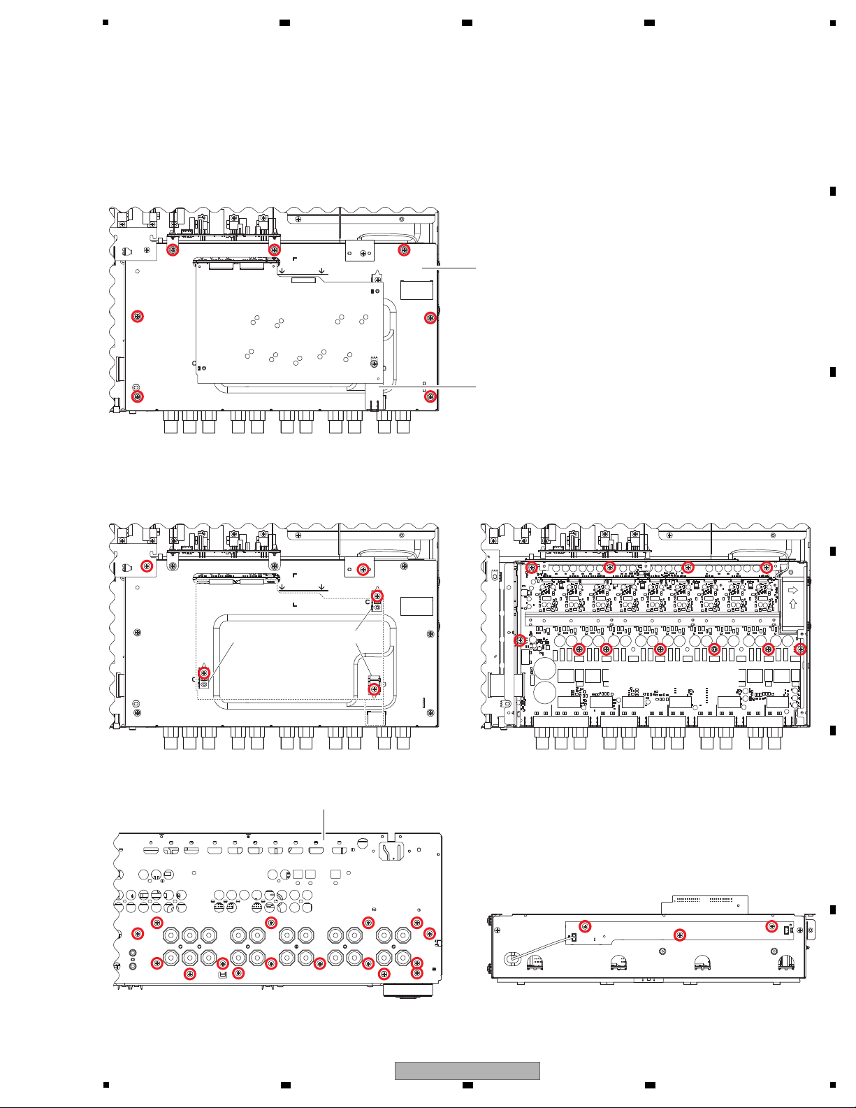
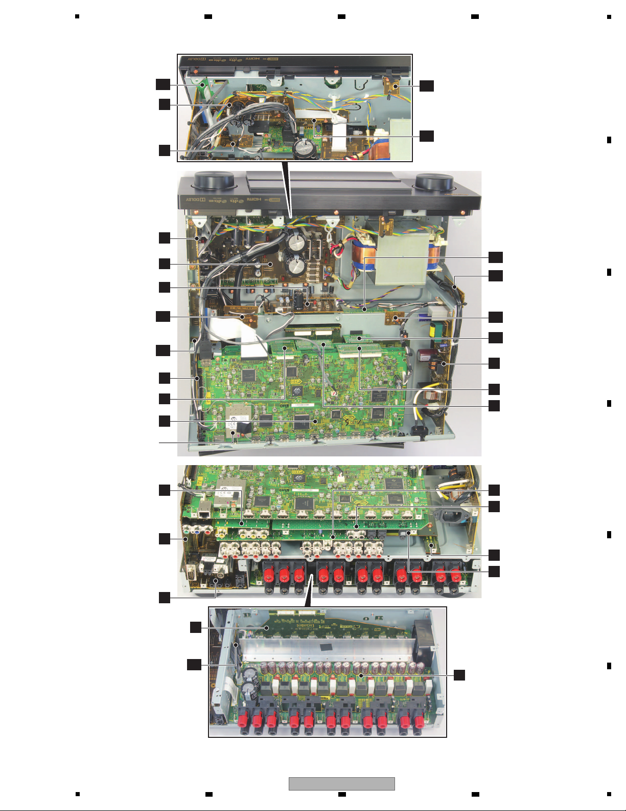
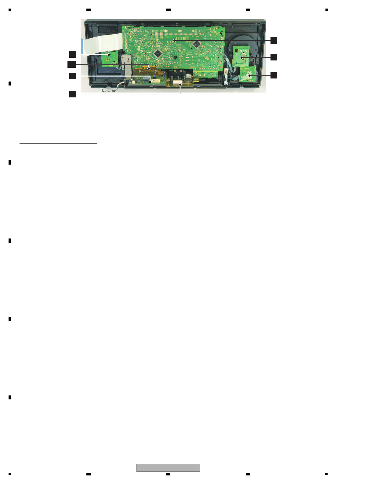
3.2 PCB LOCATIONS
6 7 8
A
B
C
D
SC-95
5
6 7 8
E
F
11
1
VOL ASSY
ENCODER ASSY
M
DISPLAY ASSY
J
POWER SW ASSY
L
FRONT HDMI USB ASSY
C
MIC HP ASSY
I
K
PANEL GUARD ASSY
AJ
NOTES: - Parts marked by “NSP” are generally unavailable because they are not in our Master Spare Parts List.
-
The > mark found on some component parts indicates the importance of the safety factor of the part.
Therefore, when replacing, be sure to use parts of identical designation.
A
B
Mark No. Description Part No.
LIST OF ASSEMBLIES
1...D AMP_SS ASSY (SC-95) AWH7114
1...D AMP_S ASSY (SC-LX59) AWH7112
NSP 1...AUDIO COMPOSITE_H ASSY (SC-95) AWR7283
2..AUDIO ASSY AWX2071
2..COMPOSITE ASSY AWX2195
2..D-AUDIO BRIDGE ASSY AWX2196
C
D
E
F
2..D-DAC BRIDGE ASSY AWX2197
2..A-DAC BRIDGE ASSY AWX2198
2..FAN CONNECT_S ASSY AWX2199
2..PRE BRIDGE_S ASSY AWX2200
NSP 1...AUDIO COMPOSITE_H ASSY (SC-LX59) AWR7284
2..AUDIO ASSY AWX2072
2..COMPOSITE ASSY AWX2195
2..D-AUDIO BRIDGE ASSY AWX2196
2..D-DAC BRIDGE ASSY AWX2197
2..A-DAC BRIDGE ASSY AWX2198
2..FAN CONNECT_S ASSY AWX2199
2..PRE BRIDGE_S ASSY AWX2200
NSP 1...PRIM DISPLAY ASSY (SC-95) AWM8410
2..DISPLAY ASSY AWX2022
2..VOL ASSY AWX2029
2..POWER SW ASSY AWX2030
2..PRIMARY ASSY AWX2031
2..ENCODER ASSY AWX2051
2..MIC HP ASSY AWX2044
2..MIC HP GUARD ASSY AWX2052
NSP 2..VREG GUARD ASSY AWX2053
NSP 2..PANEL GUARD ASSY AWX2054
NSP 1...PRIM DISPLAY ASSY (SC-LX59) AWM8411
2..DISPLAY ASSY AWX2023
2..VOL ASSY AWX2029
2..POWER SW ASSY AWX2030
2..PRIMARY ASSY AWX2032
2..ENCODER ASSY AWX2051
2..MIC HP ASSY AWX2045
2..MIC HP GUARD ASSY AWX2052
NSP 2..VREG GUARD ASSY AWX2053
NSP 2..PANEL GUARD ASSY AWX2054
NSP 1...IR BUFFER ASSY (SC-95) AWM8427
2..IR BUFFER_S ASSY AWX2097
2..BUFFER GND ASSY AWX1789
NSP 1...IR BUFFER ASSY (SC-LX59) AWM8428
2..IR BUFFER_S ASSY AWX2098
2..BUFFER GND ASSY AWX1789
12
1
2 3 4
Mark No. Description Part No.
NSP 1...INTERFACE REG_S ASSY (SC-95) AWR7302
2..INTERFACE_S ASSY AWX2135
2..IR REG_S ASSY AWX2139
2..CONNECT_S ASSY AWX2144
NSP 2..TRANS VREG STYL_S ASSY AWX1890
NSP 1...INTERFACE REG_S ASSY (SC-LX59) AWR7303
2..INTERFACE_S ASSY AWX2136
2..IR REG_S ASSY AWX2140
2..CONNECT_S ASSY AWX2145
NSP 2..TRANS VREG STYL_S ASSY AWX1890
NSP 1...PRE POWER_S ASSY (SC-95) AWR7312
2..A-REG_S ASSY AWX2168
2..V-REG_S ASSY AWX2172
2..VREG CHILD_S ASSY AWX2176
2..USB RECT_S ASSY AWX2177
2..BIND DM CABLE_S ASSY AWX1863
2..P WIRE GUARD_S ASSY AWX1864
NSP 2..FFC GUARD_S ASSY AWX1862
NSP 2..BINDFAN CABLE_S ASSY AWX1865
NSP 1...PRE POWER_S ASSY (SC-LX59) AWR7313
2..A-REG_S ASSY AWX2169
2..V-REG_S ASSY AWX2173
2..VREG CHILD_S ASSY AWX2176
2..USB RECT_S ASSY AWX2178
2..BIND DM CABLE_S ASSY AWX1863
2..P WIRE GUARD_S ASSY AWX1864
NSP 2..FFC GUARD_S ASSY AWX1862
NSP 2..BINDFAN CABLE_S ASSY AWX1865
1...IR INTERFACE_S ASSY AWX1777
2..IR INTERFACE_S ASSY AWX1777
NSP 2..IR EDGE GUARD_S ASSY AWX1779
1...DAC HIGH ASSY (SC-95) AWX2059
1...DAC HIGH ASSY (SC-LX59) AWX2060
1...COMPONENT ASSY (SC-95) AWX2101
1...COMPONENT ASSY (SC-LX59) AWX2102
1...DIGITAL MAIN ASSY (SC-95) AWX2009
2..NETWORK MODULE AXX7293
1...DIGITAL MAIN ASSY (SC-LX59) AWX2010
2..NETWORK MODULE AXX7293
1...FRONT HDMI USB ASSY (SC-95) AWX2111
1...FRONT HDMI USB ASSY (SC-LX59) AWX2112
SC-95
2 3 4
[1] Jigs List
Name
Jig No.
Remarks
Diagnosis for AUDIO ASSY, D AMP_SS(_S) ASSY
Diagnosis for AUDIO ASSY, D AMP_SS(_S) ASSY,
DIGITAL MAIN ASSY(side-B), DAC HIGH ASSY
Diagnosis for AUDIO ASSY, D AMP_SS(_S) ASSY,
DIGITAL MAIN ASSY(side-B), DAC HIGH ASSY
Diagnosis for AUDIO ASSY, D AMP_SS(_S) ASSY
Diagnosis for AUDIO ASSY, D AMP_SS(_S) ASSY
Diagnosis for AUDIO ASSY, D AMP_SS(_S) ASSY,
DIGITAL MAIN ASSY(side-B), DAC HIGH ASSY
Diagnosis for DIGITAL MAIN ASSY(side-B), DAC HIGH ASSY
Diagnosis for DIGITAL MAIN ASSY(side-B), DAC HIGH ASSY
Diagnosis for DIGITAL MAIN ASSY(side-B), DAC HIGH ASSY
Diagnosis for DIGITAL MAIN ASSY(side-B), DAC HIGH ASSY
15P FFC extension jig cable GGD1680
29P board to board extension jig cable GGD1856
5P board to board extension jig cable GGD1857
5P PH Housing ASSY extension jig cable GGD1594
4P PH Housing ASSY extension jig cable GGD1809
24P board to board extension jig cable x 2 GGD1871
23P board to board extension jig cable GGD1875
30P + 30P board to board extension jig cable GGD1682
28P board to board extension jig cable GGD1867
20P board to board extension jig cable GGD1868
[2] Lubricants and Glues List
Name
Lubricants and Glues No.
Remarks
Silicone Grease
GYA1001
Refer to “9.5 FRONT SECTION”
[3] Cleaning
Before shipping out the product, be sure to clean the following positions by using the prescribed cleaning tools.
Name skrameR.oN traPdenaelc eb ot noitisoP
Refer to “9.4 CHASSIS SECTION”.Cleaning paper GED-008Fan
5
3.3 JIGS LIST
6 7 8
A
B
C
D
E
F
SC-95
5
6 7 8
13
14
24
20
23
20
9/65
TUNER
MODULE
24
24
!
AC CORD
SECONDARY
PRIMARY
3/100
1.V+5_EV_1
2.POWLED
3.POWER KEY
4.GNDD
*2mm
1.VOLA
2.VOLB
3.GNDD
4/100
39/120
7
5
1.-B+15V
2.-B 1.V+12_DF
2.GND_DF
3.V-12_DF
4.GND_DF(S)
5.V+12_RY
6.V-12_RY
7.V-12_RY
2
1.ACWP
2.GNDV
3.GNDV
4.V+5_V
5.-VF
6.FL AC2
7.FL AC1
15/305
FAN
IR_REG_S
IR_REG_S
A-REG_S
V-REG_S
USB RECT_S
19.EXSO
18.EXSCK
17.EXOE
16.EXST
15.XOLERR
14.XBERR
13.IRMUTEA
12.IRMUTESB
11.IRMUTEFH
10.RY_FW
9.RY_AF
8.RY_CR
7.RY_FH
6.RY_B
5.AMP_TEMP
4.XTEMPSD5
3.XDCERR
2.GNDD
1.GNDD
1.HP L
2.GNDHP
3.HP R
4.GNDHP
5.AMUTE
6.XHPDET
7.XMICDET
8.V-7_A
9.GNDA
10.GNDA
11.V+7_A
12.GNDA
13.MICOUT
14.NC
15.NC
4
4
*1.00mm
55 5 555 5
1.V+8_MD
2.GND_MD
3.V-8_MD
4.GND_MD(S)
4
!
FU12!FU11!FU15
!
FU14!FU13
ADD7792-
ADD7794-
ADD7796-
D20PYY0410E
D20PYY0310E
*1.00mm
!
CN8301
CN3472
CN6001
JH6004
JH6002
CN7006
CN4000
CN4001
JP3001
CN2503
CN3051
CN6952
CN3601
CN8303
CN6801
CN6951
JP8402
CN7281
CN7502
CN6803 CN6802
CN3801CN3802
24 24
2424
*1
*4
AXM7040-
BOARD IN
FFC
2.0mm FLAT CABLE
FFC CONNECTOR
2.0mm CABLE HOLDER
*2mm
BOARD TO BOARD
CN4002
CN4003
CN4004
2
4
7
T1501
*3
5 55555 5
CN3870CN3880CN3890 CN3830CN3840CN3850CN3860
CN4700CN4100CN4200 CN4300CN4400CN4500CN4600
CN7551
CN7501
S2,S3,S9
S5,S6
S4
S1
S7
JP6001
CN6003
ADD7783-
5/60
CN8002
JA8003CN8001
24
ANOTHER CONNECTOR
CN3401
CN3371
JP6004 JP6002
JUMPER CONNECTOR
28
CN2502
20
CN3001CN2861
24
CN3902
2820
CN3794CN3792
2820
CN3793CN3791
CN3783 CN3781
CN3784 CN3782
CN7951
CN7952
24
24
24
23
CN3653
*1.00mm
24.PRESEL(W/XF)
23.V+7_A
22.V-7_A
21.GNDA
20.GNDA
19.GNDA
18.SR OUT
17.GNDA
16.SL OUT
15.GNDA
14.FR OUT
13.GNDA
12.C OUT
11.GNDA
10.FL OUT
9.GNDA
8.FH/FWR OUT
7.GNDA
6.FH/FWL OUT
5.GNDA
4.SBR OUT
3.GNDA
2.SBL OUT
1.GNDA
HDMI CONNECTOR
5
CN7553
7
*1.00mm
*1.00mm
*1.00mm
ADX7776-
7/205
1.GNDD
2.Y_IN
3.GNDD
4.CB_IN
5.GNDD
6.CR_IN
7.GNDD
8.CVBS_IN
9.GNDD
10.V+5_V
11.V+5_V
12.COMP_DET
13.SDA
14.SCL
15.GNDD
ADX7812-
7/205
JP51
5.V-12_A
4.GNDA
3.GNDA
2.V+12_A
1.V+6_AD
*4 *4
*4
FU4FU1
!!
*4
JA71_1 WHT
JA71 YEL
JA8001 JA8002
iPod Direct USB HDMI IN5
PIN JACK
JA3471
MIC IN HEADPHONE
JA3476
MCACC setup
!
FU10
*4
IR
JA7005
OUT
JA7003
12V TRG1
12V TRG2
IR IN2IR IN1
2.S7-2
1.S7-1
15.XHPDET
1.XMICDET
5.S6-2
4.S6-1
3.S5-2
2.S5-C
1.S5-1
1.S4-1
2.NC
3.S4-C
4.NC
5.S4-2
(DVR) (DVD)
JA8301JA8304
JA8601
IN1
PR
PB
YY
PB
PR
232C MONITOR IN2
OUT
1.V-5_V(NC)
2.GNDV
3.V+5_V(NC)
4.GNDV
5.NC
6.GNDV
7.NC
8.GNDV
9.DVR_OUT
10.GNDV
11.MONITOR_OUT
12.GNDV
13.DVR_IN
14.GNDV
15.NC
16.GNDV
17.TV/SAT_IN
18.GNDV
19.NC
20.GNDV
PRE OUT
1.V+5R6_EV
2.V+5R6_EV
3.V+5R6_EV
4.GNDD
5.GNDD
6.GNDD
7.RYAC
FRONT
CENTER
JA4101
RL RL
SURROUND
JA4301LRJA4901
S-BACK
for IC6001 DBUG&D.L.
CN6002
CN81
CN82
(CUXJ)
(SYXJ8,DLXJ,FXJ,AXJ5)
MAIN TRANS
J0003
J0010
J0001
J0008
SHIELD CABLE
2.GNDUSB
1.V+UN_USB
JP8001
CN3652
1.TURST
2.TUSDA
3.TUSCL
4.TUIREQ
5.NC
6.GNDT
7.TR
8.V+5T
9.TL
1.V+FAN
2.V-FAN
3.LOCK DET
D20PYY0310E
3/100
1.JOG_A
2.JOG_B
3.GNDD
JH6003
JP6003
CN3501
*2mm
JA4501
LR
55
5
CN3820
CN4900
5
CN3810
CN4800
KN6962
OUT
ZONE2
JA6701
IN5
4
1.V+5_V
2.GNDV
3.GNDV
4.V-5_V(NC)
19
CN7011
CN7662
19
19.V+12TRG
18.V+12TRG
17.GNDV
16.GNDV
15.XHPDET
14.AMUTE
13.GNDHP
12.HP_R
11.GNDHP
10.HP_L
9.GNDA
8.MICOUT
7.GNDA
6.V+7_A
5.GNDA
4.V-7_A
3.XMICDET
2.NC
1.NC
4.-B(-65V)
3.GND
2.GND
1.+B(+65V)
*1.00mm
CN7902
CN7400
CN7401
CN7663
CN7251
CN7271
CN7241
JP7291
*4
!
FU31!FU32
CN7010
ADD7790-
15/135
CN7201
!
FU22!FU21
*4
1.V+12
2.V+5_V
3.V+5_V
4.GNDV
5.GNDV
6.V-5_V(NC)
7.V-12(NC)
1.V+12
2.V+5_V
3.V+5_V
4.GNDV
5.GNDV
6.V-5_V(NC)
7.V-12(NC)
1.V+FAN
2.V-FAN
3.LOCK DET
3
CN5931
CN5932
3
*1.00mm
CN7903
1.V+FAN
2.V-FAN
3.LOCK DET
30 30
3030
JA5101
F-HEIGHT
LR
F-WIDE/B
L
R
JA3201 JA3202
SB EX1SFH
JA3103
C
BD ININ1 IN2 IN3
LAN
IN6OUT 2OUT 1 IN4
CN2003
30
CN2002
IN2
JA2006JA2004
30.V+5R6_DDD
1.DIRDATO
30.MSPDIF
1.NC
30
JA2002
OPT IN2 OPT OUT1
COAX
OPT IN1
30
IN1
20
CN2001CN2004
28
30
JA2009
24.NC
1.FHMUTE
1.S3-1
2.S3-C
3.S3-2
4.S2-1
5.S2-2
6.S9-1
7.S9-C
8.S9-2
1.S1-2
2.S1-C
3.S1-1
20.V+6_AD
1.SW2 OUT
J0004
ADD7787-
39/195
*1.00mm
7/(505/590)
ADX7821-
2/120
ADX7760-
3/215
ADX7778-
ADX7779-
4/285
4/180
ADX7780-
2/190
ADX7781-
7/180
ADX7782-
CN7552
7
7/65
ADX7783-
4/100
PF04PG-S10
PF05PG-S20
5/200
SYXJ8
DLXJ,FXJ
CUXJ
AXX7282-
*3
AXX7283-
JXJ -
MODEL TUNER
19/90
ADD7795-
J0009
*1.25mm
*1.25mm
1.XHPDET
2.AMUTE
3.GNDHP
4.HPR
5.GNDHP
6.GNDHP
7.HPL
8.GNDA
9.MICOUT
10.GNDA
11.V+7_A
12.GNDA
13.GNDA
14.V-7_A
15.XMICDET
19/360
ADX7732-
*1.25mm
ADD7793-
3/65
15.HP L
1.NC
1.GNDD
39.V+5R6_EV
3.XFANERR
2.FANCTLL
1.FANCTLH
*1.25mm
CN7009
*1.25mm
1.XFANERR
2.FANCTLL
3.FANCTLH
1.NC
2.HPRY
3.NC
4.TUIREQ
5.TURST
6.TUSDA
7.TUSCL
8.GNDD
9.DET+6AD
10.GNDD
11.GNDD
12.VLSCK
13.VLSO
14.Z2VLSO
15.Z3MUTE
16.Z2MUTE
17.SBMUTE
18.AMUTE
19.PRESEL
20.LSSN
21.XMICDET
22.PRELSSN
23.XHPDET
24.FHMUTE
5.USBPOW
4.XUSBERR
3.D+
2.D-
1.GNDD
CN9501
JA9603
JA9202
JA9605JA9604 JA9606
CN602
CN601
JA9620
CN9701
CN603
JA1601
CN9702
CN901
JA9601JA1602 JA9602
CN9202
CN1502
CN3772
CN3771
CN7554
JA7001 JA7004
JA9607
IN7
39.GNDD
1.V+5_EV
Y0020
Y0025
*1.25mm
J0007
J0002
Y0024
Y0023
Y0022
Y0021
JP8701
16.EV232TX
17.EV232RX
18.232POW
19.232CDET
20.GNDD
21.GNDD
22.V+5R6_EV
23.V+5R6_EV
*1.25mm
*1.25mm
*1.25mm
*1.25mm
*1.25mm
*1.25mm
*1.25mm
*1.25mm
529
529
5.GNDD
4.XBERR
3.TEMPERR
2.XDCERR
1.IRIN
29.V+5R6_EV
28.V+5R6_EV
27.GNDD
26.GNDD
25.XFANERR
24.FANCTLL
23.FANCTLH
22.EXSO
21.EXSCK
20.EXOE
19.EXST
18.GNDD
17.XOLERR
16.AMPTEMP
15.IRMUTEA
14.IRMUTESB
13.IRMUTEFH
12.NC
11.RYFW
10.GNDD
9.GNDD
8.RYFR
7.RYCSR
6.RYFWFH
5.RYSB
4.GNDD
3.12VTRG1
2.12VTRG2
1.12VERR
39.NC(GNDD)
38.AMPTEMP
37.XFANERR
36.IRIN
35.TEMPERR
34.XBERR
33.XDCERR
32.XOLERR
31.GNDD
30.GNDD
29.GNDD
28.XVDDERR
27.GNDD
26.232CDET
25.EV232TX5
24.EV232RX5
23.232EV
22.XSMUTE
21.LOWPOW
20.ACRY
19.GNDD
18.XNETRST
17.NETPOW
16.DVCPOW
15.XEMRST5
14.232POW
13.EVSI5
12.EVSO
11.EVSCK
10.GNDD
9.CECIO
8.EVREQI5
7.EVREQO5
6.NETWOL
5.GNDD
4.GNDD
3.GNDD
2.V+5R6_EV
1.V+5R6_EV
3
8
29 5
CN7954
CN795329CN7003
CN7004
1.GNDD
2.XBERR
3.TEMPERR
4.XDCERR
5.IRIN
5
1.V+5R6_EV
2.V+5R6_EV
3.GNDD
4.GNDD
5.XFANERR
6.FANCTLL
7.FANCTLH
8.EXSO
9.EXSCK
10.EXOE
11.EXST
12.GNDD
13.XOLERR
14.AMPTEMP
15.IRMUTEA
16.IRMUTESB
17.IRMUTEFH
18.GNDD
19.RYFW
20.GNDD
21.GNDD
22.RYFR
23.RYCSR
24.RYFWFH
25.RYSB
26.GNDD
27.12VTRG1
28.12VTRG2
29.12VERR
9.AMPTEMP
10.XSMUTE
11.LOW_P
12.ACRY
13.WUSBPOW
14.XNETRST
15.NETPOW
16.DVCPOW
17.XEMRST5
18.232POW
29.IRIN
30.TEMPERR5
31.XBERR
32.XDCERR
33.XOLERR
34.GNDD
35.GNDD
36.GNDD
37.GNDD
38V+5_EV
39.V+5_EV
1.GNDD
2.XVDDERR
3.GNDD
4.XRESET
5.232CDET
6.EV232TX5
7.EV232RX5
8.232EV
19.EVSI5
20.EVSO
21.EVSCK
22.HOTPLUG
23.CECIO
24.EVREQI5
25.EVREQO5
26.NETWOL
27.XFANERR
28.XWUSBERR
5.CEC_IO
4.XVDDERR
3.GNDD
2.GNDD
1.GNDD
5.CEC_IO
4.XVDDERR
3.GNDD
2.GNDD
1.GNDD
R
SW1&SW2F
JA3101
L
IN
19.V+5_HD
18.V+5_F
17.GNDD
16.GNDD
15.HOT_PLUG_DETECT
14.SDA_SINK
13.SCL_SINK
12.RFXC-
11.GNDD
10.RFXC+
9.RFX0-
8.GNDD
7.RFX0+
6.RFX1-
5.GNDD
4.RFX1+
3.RFX2-
2.GNDD
1.RFX2+
OUT
JA3602
JA3601
MONITOR
IN
DVR SATDVR
INOUT
IN
IN OUT
OUT
ZONE3
*BT_INSIDE(BT_OUTSIDE)
20.V+6_AD
19.V+6_AD
18.GNDAD
17.GNDAD
16.V+12_A
15.V+12_A
14.GNDA
13.GNDA
12.V+12_A
11.V+12_A
10.GNDDAS
9.FR IN
8.GNDDAS
7.FL IN
6.GNDDAS
5.SBR IN
4.GNDADS
3.SBL IN
2.GNDDAS
1.SW2 OUT
1.V+5R6_DDD
2.V+5R6_DDD
3.GNDD
4.GNDD
5.V+5_D
6.V+5_D
7.DAC0DET
8.DARST
9.I2CSW
10.SDA_DAC
11.SCL_DAC
12.GNDD
13.BADA
14.SADA
15.CADA
16.FADA
17.GNDD
18.DABCK
19.DALRCK
20.EX1ADA
21.LFE2ADA
22.EX2ADA
23.GNDD
24.DIRMCKI
25.GNDD
26.DIRMCKO
27.GNDD
28.DIRBCK
29.DIRLRCK
30.DIRDATO
1.MSPDIF
2.XDIRRST
3.UNLK
4.DIRINT
5.XTLO
6.DIRCS
7.DSPSO
8.DSPSCK
9.DSPSI
10.F96K
11.F192K
12.XADRST
13.GNDD
14.ZMCLK
15.GNDD
16.ZBCK
17.ZFADA
18.ZLRCK
19.XZ2DARST
20.ZDZF
21.GNDD
22.HDZ_MCLK
23.GNDD
24.HDZBCK
25.HDZFADA
26.HDZLRCK
27.XHDZ_DARST
28.HDZ_EMPH
29.HZDZF
30.NC
24.GGND
23.GGND
22.V-12SBL
21.V+12SBL
20.NC
19.SBL-
18.SBL+
17.V-12SBR
16.V+12SBR
15.IRMUTEB
14.SBR-
13.SBR+
12.V-12SL
11.V+12SL
10.NC
9.SL-
8.SL+
7.V-12SR
6.V+12SR
5.NC
4.SR-
3.SR+
2.V-12FHL
1.V+12FHL
24.FHL-
23.NC
22.FHL-
21.FHL+
20.V-12FHR
19.V+12FHR
18.IRMUTEFH
17.FHR-
16.FHR+
15.V-12C
14.V+12C
13.NC
12.C-
11.C+
10.V-12FL
9.V+12FL
8.IRMUTEA
7.FL-
6.FL+
5.V-12FR
4.V+12FR
3.NC
2.FR-
1.FR+
CN9502
7
1.PRESEL(W/XF)
24.GNDA
JA1603
OUT 3
8.GNDD
7.V+6R3_ROKU
6.GNDD
5.USBPOW
4.XUSBERR
3.D+
2.D-
1.GNDD
3,SHIELD
2.GNDD
1.V+6R3_ROKU
JA3102
DVR/BDR
CD
JA2505
SAT
JA2501
DVR/BDR
AXX7293
64
64
64
64
NETWORK MODULE
CN9203
CN9204
EXT. ANT.
EXT. ANT.
ADX7513-
ADH7048-
20
ADH7049-
33
EX2
28.GNDDAS
27.EX2R OUT
26.GNDDAS
25.EX2L OUT
24.GNDDAS
23.EX1R OUT
22.GNDDAS
21.SR OUT
20.GNDDAS
19.SW1 OUT
18.GNDDAS
17.FR OUT
16.GNDDAS
15.FL OUT
14.GNDDAS
13.C OUT
12.GNDDAS
11.SL OUT
10.GNDDAS
9.EX1L OUT
8.GNDDAS
7.ZR OUT
6.GNDDAS
5.ZL OUT
4.GNDDAS
3.HDZR OUT
2.GNDDAS
1.HDZL OUT
28.GNRDDAS
27.EX2 OUT
26.GNDDAS
25.EX2L OUT
24.GNDDAS
23.ZR OUT
22.GNDDAS
21.ZL OUT
20.GNDDAS
19.FR OUT
18.GNDDAS
17.FL OUT
16.GNDDAS
15.SW1 OUT
14.GNDDAS
13.C OUT
12.GNDDAS
11.SR OUT
10.GNDDAS
9.SL OUT
8.GNDDAS
7.EX1R OUT
6.GNDDAS
5.EX1L OUT
4.GNDDAS
3.HDZR OUT
2.GNDDAS
1.HDZL OUT
EXCEPT
JXJ MODEL
D-DAC BRIDGE ASSY
(AWX2197)
VOL ASSY
(AWX2029)
POWER SW ASSY
(AWX2030)
ENCODER ASSY
(AWX2051)
C
Z
I
K
L
M
S
J
E
E
1/12 -E12/12
( )
R
A
A
1/2 -A2/2
( )
T
T
1/2 -
( )
T
2/2
COMPOSITE ASSY
(AWX2195)
IR INTERFACE_S ASSY
(AWX1777)
VREG CHILD_S
ASSY
(AWX2176)
A-DAC
BRIDGE ASSY
(AWX2198)
D-AUDIO
BRIDGE ASSY
(AWX2196)
PRE BRIDGE_S
ASSY
(AWX2200)
FAN CONNECT_S ASSY
(AWX2199)
B
D
F
H
BUFFER GND ASSY
(AWX1789)
O
P
V
W
X
Y
AA
AB
Q
Q
1/6 -Q6/6
( )
U
U
1/3 -
( )
U
3/3
G
MIC HP GUARD ASSY
(AWX2052)
BIND DM CABLE_S ASSY
(AWX1863)
P WIRE GUARD_S ASSY
(AWX1864)
FFC GUARD_S ASSY
(AWX1862)
VREG GUARD ASSY
(AWX2053)
BINDFAN CABLE_S ASSY
(AWX1865)
TRANS VREG STYL_S ASSY
(AWX1890)
PANEL GUARD ASSY
(AWX2054)
IR EDGE GUARD_S ASSY
(AWX1779)
AC
AD
AE
AF
AG
AH
AI
AJ
AK
B
1/4 -B4/4
( )
N
N
1/2 -
N
2/2
( )
AUDIO ASSY
(SC-95 : AWX2071)
(SC-LX59 : AWX2072)
DAC HIGH ASSY
(SC-95 : AWX2059)
(SC-LX59 : AWX2060)
FRONT HDMI USB ASSY
(SC-95 : AWX2111)
(SC-LX59 : AWX2112)
USB RECT_S ASSY
(SC-95 : AWX2177)
(SC-LX59 : AWX2178)
DIGITAL MAIN ASSY
(SC-95 : AWX2009)
(SC-LX59 : AWX2010)
INTERFACE_S ASSY
(SC-95 : AWX2135)
(SC-LX59 : AWX2136)
MIC HP ASSY
(SC-95 : AWX2044)
(SC-LX59 : AWX2045)
DISPLAY ASSY
(SC-95 : AWX2022)
(SC-LX59 : AWX2023)
IR BUFFER_S ASSY
(SC-95 : AWX2097)
(SC-LX59 : AWX2098)
D AMP_SS ASSY (SC-95 : AWH7114)
D AMP_S ASSY (SC-LX59 : AWH7112)
PRIMARY ASSY
(SC-95 : AWX2031)
(SC-LX59 : AWX2032)
A-REG_S ASSY
(SC-95 : AWX2168)
(SC-LX59 : AWX2169)
IR REG_S ASSY
(SC-95 : AWX2139)
(SC-LX59 : AWX2140)
V-REG_S ASSY
(SC-95 : AWX2172)
(SC-LX59 : AWX2173)
CONNECT_S ASSY
(SC-95 : AWX2144)
(SC-LX59 : AWX2145)
COMPONENT ASSY
(SC-95 : AWX2101)
(SC-LX59 : AWX2102)
Therefore, when replacing, be sure to use parts of identical designation.
When ordering service parts, be sure to refer to "EXPLODED VIEWS and PARTS LIST" or "PCB PARTS LIST".
The > mark found on some component parts indicates the importance of the safety factor of the part.
!
*4
*1
!
MODEL AC CORDMAIN TRANS
FU11,FU12 FU13,FU14 FU15FU1 FU4 FU31,FU32FU21,FU22FU10
MODEL
DLXJ
CUXJ
SYXJ8
JXJ
FXJ
SYXJ8
CUXJ
JXJ
FXJ
SC-LX59
SC-LX59
SC-LX59
REK1154(10A/125V)
REK1154-
(10A/125V)
AEK1061(T5A L/250V)
AEK1061(T5A L/250V)
DEK1045(T10A L/250V)
REK1139(T2A H/250V)
REK1139(T2A H/250V)
REK1104(T4A H/250V)
REK1104(T4A H/250V)
REK1139(T2A H/250V)
REK1151(6A/125V)
REK1151(6A/125V)
AEK1061(T5A L/250V)
AEK1061(T5A L/250V)
AEK1061(T5A L/250V)
REK1143(1.25A/125V)
REK1143(1.25A/125V)
AEK7073(T1A L/250V)
AEK7073(T1A L/250V)
AEK7073(T1A L/250V)
REK1142(1A/125V)
REK1142(1A/125V)
AEK7072(T800mA L/250V)
AEK7072(T800mA L/250V)
AEK7072(T800mA L/250V)
REK1143(1.25A/125V)
REK1143(1.25A/125V)
AEK7073(T1A L/250V)
AEK7073(T1A L/250V)
AEK7073(T1A L/250V)
REK1143(1.25A/125V)
REK1143(1.25A/125V)
REK1144(1.6A/125V)
REK1144(1.6A/125V)
AEK7072(T800mA L/250V)
AEK7072(T800mA L/250V)
ATS7482-A
ATS7483-A
ATS7485-A
ATS7483-A
ATS7454-A
ADG7123-A
ADG7120-A
ADG7121-A
ADG7123-A
ADG7118-A
AEK7072(T800mA L/250V)
SC-LX59-K
SC-LX59-S
SC-LX59-K
SC-LX59-S
SC-LX59
SC-LX59
SC-LX59
AEK7073(T1A L/250V)
AEK7073(T1A L/250V)
AEK7073(T1A L/250V)
SC-95
SC-95
DLXJ
!
with same parts (safety regulation authorized) of identical designation.
mark found on some component parts should be replacedThe
CAUTION - FOR CONTINUED PROTECTION AGAINST RISK OF FIRE,
REPLACE WITH SAME TYPE AND RATINGS OF FUSE.
*Furnished parts
MODEL MICROPHONE REMO-COM iPod CABLE
DLXJ
SC-LX59-K
SC-LX59-S
SC-LX59
SC-LX59
SYXJ8
CUXJ
JXJ
SC-LX59
SC-95
FXJ
APM7011- AXD7725-
APM7011-
APM7011-
APM7011-
APM7011-
AXD7725-
AXD7726-
AXD7725-
AXD7725-
4. BLOCK DIAGRAM
F
E
D
C
B
A
4. BLOCK DIAGRAM
4.1 OVERALL WIRING DIAGRAM
1
2 3 4
SC-95
1
2 3 4
4.2 BLOCK DIAGRAM FOR AUDIO BLOCK
COAX2(SAT/CBL)
OPT IN1(TV)
OPT IN2(DVR/BDR)
COAX1(DVD)
IC2009
8ch DAC
ES9016S
TX1
JA2002
JA2004
JA2006
MIC
SAT/CBL
TUNER Module
CD
PREOUT FL/FR
PREOUT SW1
PREOUT SL/SR
PREOUT SBL/SBR
DVR OUT
SP FL/FR
SP C
SP SL/SR
SP SBL/SBR
HP
SW DownMix
JA3471
IC2701, IC2702
JA2505
SW PRE Amp
IC2751
<<POWER AMP>>
JA2504
JA3476
JA4101
JA4101
JA4301
JA4501
JA3101
JA3101
JA3201
JA3201
PREOUT C
JA3103
DVR
JA2501
ZONE3 OUT
JA3206
HEADPHONE Amp
IC6821,
IC6841
IC6801
IC6861,
IC6881
IC6901,
IC6921
<<PREOUT>>
<<AUDIO ZONE OUT>>
MIC Amp
IC3471
IC2032
(ZONE2)
LPF
I2S
A/D BUFFER
IC2033, IC2035
OPT OUT1
IC2801
JA2009
JA2505
PREOUT TML/TMR
JA3201
IC3221
PRE SELECTOR
SP TML/TMR
JA4901
IC2003
DIR&DIT
AK4118AEQ
IC3271
IC7491
TMEX1
SELECTOR
IC2027
ADC
PCM1804DB
I2S(DATA)
I2S(BCK,LRCK)
SW PRE Amp
IC2751
JA3102
PREOUT SW2
PREOUT EX1L/EX1R
JA3202
IC3272
(FL,FR)
IC7451,
IC7471
SP EX1L/EX1R
JA5101
ZONE2
ZONE3
ZONE3
ZONE2 OUT
JA6701
IC2026
ZONE2 DAC
AK4388ET
ARC
IC2006
BUFFER
IC2007
BUFFER
I2S I2S
IC2010
8ch DAC
ES9016S
I-V
&
LPF
I-V
&
LPF
X2001
80MHz
OSC
(Zone2 L,R)
(S&FH DATA)
(BCK,LRCK,F&C DATA)
(BCK,LRCK)
IC2034
IC2031
IC2029
IC2030IC2037
IC2028
IC2002
IC2010
IC2009
V+6V_ADAD
IC2026,
IC2027
IC2009
,
IC2010,
X2001
IC2027
IC2009
,
IC2010
V+5V_D
IC2003, IC2004,
IC2005, IC2006,
IC2007
IC2001,
IC2003
1.2V
1.2V
3.3V
3.3V
3.3V
3.3V
5V
<<POWER AMP
INPUT BUFFER>>
LPF
IC2038
HD ZONE DAC
AK4388ET
I2S
IC2039
(HD ZONE2)
(HD Zone L,R)
IC2038,
IC2501
Selector / Volume / PRE Amp
BD3473KS2
IC3273
Selector / Volume / PRE Amp
BD3473KS2
IC2011, IC2012, IC2021(SR,EX1R)
IC2013, IC2014, IC2022(FR,SW1)
IC2015, IC2016, IC2023(C,FL)
IC2019, IC2020, IC2025(EX1L,SL)
IC2051, IC2052, IC2053 (SBL,SBR)
IC2041, IC2042 (SW2)
IC2017, IC2018, IC2024 (EX2L,EX2R)
(SBL,SBR,SW2,EX2L,EX2R)
(SB, EX2, SW2 DATA)
IC2036
X2001
3.3V
V+5R6_DD D
(C,SW1,SL,SR,EX1L,EX1R)
F
C
S
EX1
SW1
SW2 DownMix
IC2703, IC2704
(EX2L,EX2R))
(SBL,SBR,SW2)
SW2
SB
EX2
JA3202
PREOUT EX2L/EX2R
IC2802
BD3812F
Z2VOL
DVR
TMEX1
Refer to the “4.4 BLOCK DIAGRAM FOR DIGITAL MAIN AUDIO BLOCK”
Except Japanese Model
DIGITAL MAIN ASSY
E
DAC HIGH ASSY
B
MIC HP ASSY
I
MIC HP ASSY
I
AUDIO ASSY
A
D AMP_SS(_S) ASSY
Q
IR BUFFER_S
ASSY
N
5
6 7 8
SC-95
15
F
E
D
C
5
6 7 8
B
A

16
IC9703
DSP
D808K013DPTP456
ETHERNET
IC9602
HDMI SW
Silicon Image
"SiI9589-3"
Deneb
IC909
Video Decoder
Analog
Devices
"ADV7181C"
IC1204
IP.SCALER
Marvell
"88DE2750"
EVENT ucom
RENESAS
IC103
SerialFLASH
64Mb
IC603
Gate Array
SEIKO EPSON
"PE7008A"
Media Processor
"AXX7293-"
IC9202
Serial FLASH
128Mb
IC9206
iPod
Authentication
APPLE
(RENESAS)
"H337S3959"
2
2
2
2
36.864MHz
28.63636MHz
HDMI IN6
HDMI IN3
HDMI BDIN
HDMI IN1
HDMI IN2
HDMI IN5
DDC
Buffer
COMPOSITE
COMPONENT
Pb
Pr
COMPOSITE
USB(FRONT)
HDMI OUT1
22.5792MHz
POWER SUPPLY BLOCK Diagram
(DCDC,LDO)
IC1212
DDR2
512Mb
Y
24.576MHz
HDMI IN7
/MHL
IC9702
SDRAM-166
64Mb(8Mx16)
IC9704
SeriFlash
16Mb
HDMI ZONE
/OUT3
24 MHz24.576 MHz
IC1609
HDMI SW
"MN864788"
IC1602
4k2k Upscaler
MN864787
IC101
uCOM
"R5S726B0D216FP"
IC9002
DSP
CS49844A
IC9001
SDRAM-166
64Mb(8Mx16)
IC9004
SeriFlash
32Mb
IC102
SDRAM
64Mb
HDMI OUT2
TMDS
DIGITAL VIDEO
CEC
ANALOG VIDEO
CLOCK
DIGITAL AUDIO
CEC
COMPONENT-Y
COMPONENT-Pb
COMPONENT-Pr
20 MHz
27 MHz
27 MHz
12 MHz
For PQLS
BT
Wi-Fi
LAN PHY
YCbCr422
YCbCr422
COMPOSITE ASSY
H
COMPONENT ASSY
G
FRONT HDMI USB ASSY
C
DIGITAL MAIN ASSY
E
FRONT HDMI USB ASSY
C
DISPLAY ASSY
J
COMPOSITE ASSY
H
COMPONENT ASSY
G
F
E
D
C
B
A
4.3 BLOCK DIAGRAM FOR DIGITAL MAIN VIDEO BLOCK
1
2 3 4
SC-95
1
2 3 4
5
S(C
6
)
IC1
806
6 7 8
SC-95
DAC HIGH ASSY
B
PCM1804DB
IC2003
DIR
COAX 1
AK4118AEQ8
COAX 2
OPT 1
OPT 2
DIGITAL MAIN ASSY
E
NMCK
NBCK
NLRCK
NFDAT/NDSDFL
NMP
NSLR/NDSDFR
CH0AMCLK
CH0ABCLK
CH0ALRCLK
CH0ASD0
CH0ASD1
CH0ASD2
CH0ASD3
CH0ASPDIF
CH1ABCLK
CH1ALRCLK
CH1ASD0
Q6
Q5
Q4
D4
D1
D0
NC_LFE
DSPB_BCK
DSPB_LRCK
DSPB_BDT
PHDZAMCLK
PHDZBCK
PHDZLRCK
PHDZFDT
HDZBCK
HDZLRCK
HDZFDT
P1MCLK
P1_BCK
P1_LRCK/DSDSL
P1_HFDT/DSDFL
P1_CDTI/DSDLFE
P1_SDTI/DSDC
P1_BDTI/DSDSR
P1_DSDFR
D2B_BCK
D2B_LRCK
D2B_FDT
AXX7293
IC1602
MN864787
IC2027
ADC
MSPDIF
DAUX
BICK
LRCK
SDTO
MCKO1
IC1603
AND(VHC08)
IC2006
AND (VHC08)
XTI
DIRBCK
DIRLRCK
DIRDATO
NBCK
NLRCK
NFDAT/NDSDFL
NC_LFE
P1_BCK
P1_LRCK/DSDSL
P1_HFDT/DSDFL
P1_CDTI/DSDLFE
NSLR/NDSDFR
P1_SDTI/DSDC
P1_BDTI/DSDSR
P1_DSDFR
HDMCK
HDMCK
IC1601
AND(VHC08)
IC1521
AND (SH08)
HDMI/NW SELECTOR
IC9101
SEL(LHC157)
IC1815
SEL(LHC157)
DIRLRCK
DIRDATO
L: NETMCKH: HDMI
DIRBCK
NETDSDMCK
DSD28X56
IC1511
×8 or 4
USBDMCK
IC1815
SEL(LCX157)
D_HN_BCK
D_HN_LRCK
D_HN_FDT/DSDFL
HN_CDTI/DSDLFE
HN_SDTI/DSDC
HN_BDTI/DSDSR
HN_DSDFR
ZONE DAC SELECTOR
DIRMCKI
IC1804
AND (LCX08)
IC1509
SEL(VHC126)
DUBCK
DULRCK
DUDT
IC9005
VHC4040
DSD_LRCK
HN_SDTI/DSDC
HN_DSDFR
HN_CDTI/DSDLFE
HN_BDTI/DSDSR HN_BDTI/DSDSR
DSD_IN
IC9006
SEL(VHC157)
DIRMCK
NETMCK
NETMCK
HDMCK
D_HN_BCK
D_HN_LRCK
D_HN_FDT/DSDFL
D_HN_DSDFR
DUBCK
DURLRCK
DUDT
HN_DIR_BCK
HN_DSD_LRCK
HN_HFDT/DSDFL2
HN_SDTI/DSDFR
HN_BDTI/DSDSL
HN_SDTI/DSDC
HN_CDTI/DSDLFE
L: NETWORK
ZNET
IC1814
SEL (LCX157)
XXTL0
24.576MHz
22.5792MHz
DAI3_SCK
DAI3_LCK
DAI3_D0
DAI1_SCK1
DAI1_LRCK1
DAI1_D0
DAI1_D1
DAI1_D2
DAI1_D3
DAI1_D4
DAI1_D5
SPDIF
AMCLK
HD ZONE DAC
SELECTOR
HDZDACSEL
IC1818
SEL (LCX157)
MASTER CLOCK SELECTOR BLOCK
IC1806
SEL(VHC126)
H: DIR
L: NET/HDMI
DIRMCK
IC1516
SEL(VHC157)
IC9002
24.576 MHz
1stDSP
CS49844A
DAO1_MCLK
DAO1_SCK1
DAO1_LCK1
DAO1_D0 D1FDT
DAO1_D2 D1CDT
DAO1_D1 D1SDT
DAO1_D3 D1EX1DT
DAO1_D4 D1EX2DT
DAO1_D5 D1EX3DT
I2S SYSCLK
FLG I2S BCK,LRCK
H: NW
L: HDMI
IC1804
AND(LCX08)
24PQLS
22PQLS
DAZDB
D2MCLK
FMCLK
DSP THROUGH PCM/DSD SWITCHING BLOCK
D808K013DPTP456
ACLKR1
AFSR1
D1FDT AXR1[0]
D1CDT AXR1[1]
D1SDT AXR1[2]
D1BWDT AXR1[3]
D1HWDT AXR1[4]
D1DMDT AXR1[5]
ZMCLK
ZONE-I2S (LR)
D2BCK
D2LRCK
D2FDT/DSDFL
D2CDT/DSDFR
24.0 MHz
IC9703
2ndDSP
AXR0[7]D2FDT
AXR0[8]D2CDT
AXR0[9]D2SDT
AXR0[10]D2BWDT
AXR0[12]D2HWDT
HDZ DAC
DABCK
DALRCK/DSDFL
DAFDT/DSDFR
DACDT
H : DSP THROUGH ROUTE
L : DSP ROUTE
DSPPASS
IC1501
SEL(LCX157)
AHCLKX0
D2BCK
ACLKX0
D2LRCK
AFSX0
D2FDT/DSDFL
D2CDT/DSDFR
D2SDT
D2BWDT
D2HWDT
D2SW2DT
AXR0[13]
D2EXDT
AXR0[11]
IC2026
Z2 DAC
FL/FR
IC2038
FL/FR
IC2007
OR (VHC32)
H : DSD
L : PCM
DSDXPCM
IC1515
SEL(LCX157)
IC1616
AND(VHC08)
DABCK
DALRCK/DSDFL
DAFDT/DSDFR
DACDT
IC1503
SEL(LCX157)
IC1507
SEL(WH157)
FR_PRE_ON
IC2010
DAC
ES9016
FL/FR
C/LFE
SL/SR
FHL/FHR
80MHz
IC2009
DAC
ES9016S
SBL/SBR
LFE2
RYAC
NET
POW
DIR
POW
DVC
POW
4.4 BLOCK DIAGRAM FOR DIGITAL MAIN AUDIO BLOCK
5
6 7 8
17
27MHz
F
E
D
C
B
A
1
DIGITAL MAIN ASSY
COMPONENT ASSY
E
G
COMPOSITE ASSY
H
COMPOSITE ASSY
H
DVR
TV SAT
SH uCOMSH uCOM
"R5S726B0D216FP"
VDECVDEC
"ADV7181C"
LPF
LPF
LPF
50
47
14
16
17
19
20
22
31
38
33
32
30
29
28
37
39
26
IC8301
NJW1328FH2
CDET
I2C
MONITOR OUT
DVR OUT
IN1
2 3 4
4.5 BLOCK DIAGRAM FOR VIDEO BLOCK
A
B
C
D
E
SC-95
F
18
1
2 3 4
5
V+3R3_ MA
V+1R25 _MA
V+2R5_ MA
DVCPOW
NETPOW
V+1R2_ HD
V+1R1_ PA
DVCPOW
JA1601
DVCPOW
JA1602
JA1603
V+5_MH L
JA9607
JA9620
V+1R8_ SC
V+1_SC
V+1R8_ VD
V+3R3_ DSP
DIRPOW
DIRPOW
V+1_D1
DIRPOW
V+1R3_ D2
V+3R3_ OS
DIRPOW
V+1R2_ NW
V+3R3_ NW
NETPOW
V+2R5_ NW
V+5_EV
V+5_DS P
DIRPOW
V+3R3_HHH(MA)
V+5R6_EV( DDD)
V+1R8_HHH
V+1R8_NW
NW Module
AXX7293
IC101
SH2
R5S726B0D216FP
IC103
Serial Flash
IC102
SDRAM
IC603
Gate Array
PE7008A
IC9002
CS49844A-CQZ
IC9001
SDRAM
IC9004
Serial Flash
IC909
VIDEO De corde r
ADV7181CBSTZ
IC9515
1.25V LDO
S-1172B1C-U5
IC9602
HDMI SW
SiI9589CTUC-3
IC1602
HDMI Tx
MN864787
IC9511
5V LDO
MM3529A50
IC9502
LDO
S-13A1 A00-E6
IC9518
1V LDO
S-1172B10
IC9508
2.5V LDO
MM3529A25
V+5_HD
IC9505
1.8V LDO
MM3529A18
X1501, X1502
XTAL
IC9408
3.3V DCDC
MM3542BF
IC9403
1.1V DCDC Converter
MM3543BH
V+3R3_DSP
IC9603
Current SW
BD82065FVJ
IC451
3chDCDC
Converter
TPS65251RHA
IC9406
5V LDO
MM3411A50
232C
Mute Buffe r
IC9703
DSPD80 8K013DPTP 456
IC9702
SDRAM
IC9704
IC9407
2.5V LDO
MM3529A25
IC1615
5V LOADSW
BD2242G-G
HDMI OUT1
HDMI OUT3/HDZONE
IC1605
5V LOADSW
BD2242G-G
SMPS
Other Circuits
V+5R6_EV
Refer to
MAIN Transformer part
A
CN9501
CN9502
HDMI IN7/MHL
IC9523
1.2V Ripple Blocker
MIC94325YMT
IC1609
HDMI TX SW 4in2
MN864788
IC1610
5V LOADSW
BD2242G-G
HDMI OUT2
IC1204
VIDEO
PROCESSOR
88DE2750
IC1212
DDR2 for
Scaler
IC9402
1V LDO
S-1172B10
IC9404
1.8V LDO
MM3529A18
IC9513
3.3V LDO
NJM2846DL3-33
IC9514
1.3V Ripple Blocker
MIC94325YMT
IC9512
3.3V LDO
NJM2872BF33
IR
IC9504
5V LDO
MM3529A50
EVENT CPU
V+5_EV
IC6001
CN7903
FFC
CN6001
V+5_EV
V+5R6_ EV
CN7954
CN7004
CN7952
CN603
IC8601
RS232C
232POW
IC2003
DIR + DIT
Peripheral
AK4118AEQ
IC2026
Zone2 DAC
AK4388EF
IC2027
A/D Converter
PCM1804DB
IC2031
3.3V LDO
NJM2872BF3
C
N
2
0
0
4
V+3R3_ DA
V+5_DA
C
N
3
7
9
1
V+6_AD
IC2002
3.3V LDO
NJM2881F33
C
IC2034
5V LDO
NJM2845DL1-05
V+5_D
V+3R3_ D
IC2029
3.3V LDO
NJM2872BF3
IC2030
3.3V LDO
S-1172B33-E6
IC2009
SUB DAC
ES9016S
V+3R3_A
IC2010
MAIN DAC
ES9016S
V+3R3_DA2
IC2037
1.2V LDO
S-1172B12-E6
V+1R2_ A2
IC2028
1.2V LDO
S-1172B12-E6
V+1R2_ A
CN8301
CN901
IC7902
5V LDO
MM3411A50
IC2038
HDZone DAC
AK4388EF
IC2040
3.3V LDO
S-1172B33-E6
V+3R3_DA3
CN601
FFC
CN7902
CN9701
CN2001
CN3784
CN3783
IC2036
3.3V LDO
NJM2872BF33
V+3R3_ DAOSC
X2001
XTAL
DAC HIGH ASSY
FRONT HDMI
USB ASSY
DIGITAL MAIN ASSY
INTERFACE_S ASSY
COMPONENT ASSY
DISPLAY ASSY
PRIMARY ASSY
V-REG_S ASSY
CONNECT_S ASSY
B
C
E
F
G
J
R
U
W
D-DAC
BRIDGE
ASSY
Z
6 7 8
4.6 BLOCK DIAGRAM FOR POWER BLOCK (1)
A
B
C
D
5
6 7 8
SC-95
E
F
19
1
MAIN
Transformer
RECTIFIER
D7501-7504
3
3
19
+
-
+
-
V+12 A
V-12A
2
for FL
Q3001
Q3002
Q3901
V+12 _A
V-12_A
TU NER MODULE
CN3902
FFC
V+5_ T
V+7_ A
V- 7_ A
V-12_A
V+12_A
V+5_ V
CN8301
CN901
V+5_ V
Except Japanese
Model
V-7_A
V+7_ A
V+12 TRG
FL_AC2
-VF
V+5_ V
RECTIFIER
D7241-7244
RECTIFIER
D7271-7274
IC7271
NJM78M08FA
IC7272
NJM79M08FA
RECTIFIER
D7251-7254
IC7251
NJM78M12FA
IC7252
NJM79M12FA
CN7201
8
+
+
+
-
-
CN7241CN7271JP7291
FAN
-B+15V
V+8_ MD
V-8_MD
V+FAN
V-FAN
V+12 DF
V-12DF
RECTIFIER
D7400,7401
3
CN7400
+
-
+B
-B
CN4001CN4002CN4003
V+64 V
V-64V
VSS+12V
V+5V
V-5V
V+12 V
V-12RY
V+12 RY
V-12V
V+12 **
V-12**
CN38 01,3802
CN68 02,6803
CN3810-3890
CN4*00
V+7_ A
V-7_A
CN7401
IC4*03
NJM2830U1-12
Driver IC VCC
CN5931
CN5932
+
CN3653
CN3652
IC7241
NJM78M15FA
FFC
CN3472
CN7663
CN7662
CN7011
5
RECTIFIER
D7560
V+12
IC8701
NJM78M05FA
V+5
CN7552
JP8701
IC7501
NJM78M12FA
RECTIFIER
C7557,
D7554,7551
V+12 TRG
V+7_A
V-7_A
RECTIFIER
D7557,7558,
7559
CN7010
CN3051
CN2503
FFC
CN4004
CN7251
V+12RY
V-12RY
CN6952
CN6951
CN6801
A
B
B
IC4008
NJM78M05DL1A
IC4009
NJM79M05DL1A
CN7554
JP8402
V+5
CN7553
JP6001
FL_AC1
CN7502
CN3001
CN3792
CN3791
CN2004
C
V+6_ AD
V+6_ AD
CN7501
IC7502
NJM79M12FA
IC7501
NJM78M12FA
IC7521
NJM78M06FA
IC2034
NJM2845DL1-05
V+5_ DA
CN7551
IC4003
NJM78M05DL1A
V+5V_ S
V+5_ USB
USB +5V
Supply
V+UN _USB
HDMI V+5MHL
Supply
JP8001
IC9603
BD82065FVJ
(Load SW)
JA9607
CN9502
CN8001
IC8004
BD9329EFJ
(DC-DC Conv.)
CU : 6.3V
exept CU : 5.1V
JA8001
IC8002
BD82065FVJ
(Load SW)
V+5_ MHL
RECTIFIER
D3651
Q7211
Q7212
AA
AB
AUDIO ASSY
DAC HIGH ASSY
FRONT HDMI USB ASSY
USB RECT_S ASSY
DIGITAL
MAIN ASSY
INTERFACE_S ASSY
COMPONENT ASSY
MIC HP
ASSY
DISPLAY ASSY
IR BUFFER_S
ASSY
IR
INTERFACE_S
ASSY
D AMP_SS(_S) ASSY
A-REG_S ASSY
IR REG_S ASSY
V-REG_S ASSY
VREG CHILD_S ASSY
A-DAC
BRIDGE
ASSY
PRE BRIDGE_S
ASSY
FAN CONNECT_S ASSY
A
B
C
D
E
F
G
I
J
N
P
Q
S
T
U
V
X
DIGITAL MAIN ASSY
E
2 3 4
4.7 BLOCK DIAGRAM FOR POWER BLOCK (2)
A
B
C
D
E
F
20
1
2 3 4
SC-95
5
This is just for general reference and does not including every single case.
No Power
Error Indications ?
Stand by
No
Yes
Yes
No
Refer to the
“5.2 [4] Error Indocations”
Jump to “No FL DISPLAY”
Fuse FU4 OPEN ?
No
Yes
Diagnose or replace
PRIMARY ASSY
Check PRIMARY ASSY
JP51-1,2,3pin or DIGITAL
MAIN ASSY
CN9501-1,2,3pin +5.6V
No
Check DIGITAL MAIN ASSY
CN601-1,2pin +5.6V
Check +5.6V line on DIGITAL MAIN ASSY
or replace DIGITAL MAIN ASSY
Check DISPLAY ASSY
C6017 +3.3V
Replace DISPLAY ASSY
or replace L6001
Yes
Yes
Yes
Yes
Yes
Check DISPLAY ASSY
L6001 +5.0V
Replace DISPLAY ASSY
or replace IC6002
Check DISPLAY ASSY
IC6001-10pin +4.9V (XRESET)
Check the signal path of XRESET
or replace DISPLAY ASSY
Check DISPLAY ASSY
IC6001-32pin (POWKEY)
HL when press power key
Check the signal path of POWKEY
Check DISPLAY ASSY
CN6001-16pin (DVCPOW)
LH when press power key
Check the signal path of DVCPOW
No
Check DISPLAY ASSY
CN6001-12pin (ACRY)
LH when press power key
No Problem
Replace DISPLAY ASSY
Check the signal path of ACRY
Check PRIMARY ASSY
JP51-7pin (ACRY)
LH when press power key
Does RY71 turn on
when press power key ?
Remove AC code and remove
CN9501. Insart AC code and
check JP51-1,2,3pin, +5.6V
Diagnose or replace
PRIMARY ASSY
No
Diagnose the power supply path of
V+5R6_EV after PRIMARY ASSY
Yes
Check V-REG_S ASSY
CN7902-38,39pin +5.6V
Replace FFC
(DIGITAL MAIN ASSY to V-REG_S ASSY)
Check V-REG_S ASSY
CN7903-1,2pin +5.0V
CN7903-36pin +4.9V(XRESET)
Check DISPLAY ASSY
CN6001-38,39pin +5.0V
CN6001-4pin +4.9V(XRESET)
Replace V-REG_S ASSY,
D7901, IC7901, IC7902 or IC7903
Replace FFC
(V-REG_S ASSY to DISPLAY ASSY)
No
No
No
No
No
Yes
No
Yes
No
No
Yes
No
Yes
No No Problem
Replace DISPLAY ASSY
Yes
Yes
No
Yes
Yes
No
Yes
Check the signal path of ACRY DISPLAY ASSY V-REG_S ASSY
DIGITAL MAIN ASSY PRIMARY ASSY
Check the circuits around RY71 or replace PRIMARY ASSY
Check DIGITAL MAIN ASSY
CN601-16pin (DVCPOW)
LH when press power key
Check the signal path of DVCPOW DISPLAY ASSY V-REG_S ASSY
DIGITAL MAIN ASSY
Diagnose or replace
DIGITAL MAIN ASSY
6 7 8
5. DIAGNOSIS
5.1 DIAGNOSIS FLOWCHART
NO POWER
A
6 7 8
5
SC-95
B
C
D
E
F
21
1
This is just for general reference and does not including every single case.
No FL DISPLAY
Dimmer ?
No
"FL OFF"LED light on ?
Yes No
JP6001 6,7pin 4.3Vac
Yes
No
V6001(FL Display)
damage
Yes
No
Yes
Replace V6001
(FL Display)
Check the power supply path of FL AC1
and AC2 or replace DISPLAY ASSY
Check DISPLAY ASSY
Check DISPLAY ASSY
JP6001 5pin -30V (VF)
4pin +5V
No
Yes
Check the path of V+5_V,-VF
(Signal path is same as FL AC1 and AC2)
All NG
All NG
Replace MAIN TRANS
Diagnose or replace
NG ASSY
Other results
Other results
Diagnose the circuits
(around D6010)
or replace DISPLAY ASSY
Diagnose around IC6003
NG
Replace IC6003
or DISPLAY ASSY
No Problem
Replace V6001(FL Display)
or DISPLAY ASSY
Check DISPLAY ASSY
Check DISPLAY ASSY
IC6003(FL uCOM)
51 pin oscillating (2 MHz)
Yes
No
No
Replace IC6003
or DISPLAY ASSY
Diagnose VREG CHILD_S
ASSY
(around IC8701:V+5_V) and
V-REG_S ASSY (around
D7563, D7564:-VF)
Replace VREG CHILD_S ASSY
or replace V -REG_S ASSY
Check the path of FL AC1 and AC2
DISPLAY ASSY
V-REG_S ASSY MAIN TRANS
Check DISPLAY ASSY
V6001(FL Display)
1,62pin 4.3Vac
Check DISPLAY ASSY
IC6003(FL uCOM)
56 pin +5.0V (V+5_V),
52 pin +5.0V (XFLRST)
Check the path of V+5_V or XFLRST
or replace DISPLAY ASSY
No
Yes
2 3 4
NO FL DISPLAY
A
B
C
D
E
F
22
1
2 3 4
SC-95
5
EXT STEREO mode : 2ch signals are distributed to all channels.
OPTIMUM Surr mode : Surround mode of headphones
No sound from speakers (Single channel - Check only the signal path of the relevant channel. Plural channels
- There may be troubles with power source, control signals: MUTE, DET and others. Bad connection of cables
and connectors should be also considered.)
No sound only from front
channels (L/R 2 channels)
The sound of the relevant
channel does not come from Preout.
Sound comes from speakers in Pure Direct by
applying a signal to analog input terminal.
The signal of the relevant channel
exists in PRE BRIDGE_S ASSY.
Check the path of
the relevant
channel in AUDIO
ASSY.
Check the signal path of the relevant channel in
IR BUFFER_S ASSY, or check the path of the power supply
to the relevant channel.
In EXT STEREO, the signal of the
relevant channel does not exist in
A-DAC BRIDGE ASSY.
Check the path of the relevant
channel in AUDIO ASSY.
Check the signal path of the relevant channel in
IR INTERFACE_S ASSY, or check the path of the power
supply to the relevant channel.
The signal (DATA, BCK, LRCK) of
the relevant channel does not exist
in D-DAC BRIDGE ASSY.
Check the path of the relevant
channel in DAC HIGH ASSY.
Check the path of the relevant channel in
D AMP_SS(_S) ASSY.
Check the path of the relevant
signal in DIGITAL MAIN ASSY.
No sound only from Preout (Single channel - Check only the signal path of the relevant channel. Plural channels
- There may be troubles with power source, control signals: MUTE, DET and others. Bad connection of cables
and connectors should be also considered.)
No sound only in DVROUT - Check the relevant path in AUDIO ASSY .
No sound from speakers additionally
Check the path of the relevant channel
in AUDIO ASSY.
In EXT STEREO, the signal of the relevant channel does not exist in
A-DAC BRIDGE ASSY.
Check the path of the relevant channel
in AUDIO ASSY.
The signal (DATA, BCK, LRCK) of the relevant channel does not exist
in D-DAC BRIDGE ASSY.
Check the path of the relevant channel
in DAC HIGH ASSY.
Check the path of the relevant signal in DIGITAL MAIN ASSY.
No No No
Yes
Yes
Yes
Yes
Yes
Yes
OK
OK
No
No
No
Yes
Yes
Yes
No
No
No
No sound only in COAX and OPT input (Single channel - Check only the signal path of the relevant channel.
Plural channels - There may be troubles with power source, control signals: MUTE, DET and others.
Bad connection of cables and connectors should be also considered.)
Check the path of the relevant channel
in DAC HIGH ASSY.
Check the path of the relevant signal in DIGITAL MAIN ASSY.
Yes
No
Check the path of the relevant channel
in DAC HIGH ASSY.
Yes
No
Apply a signal to analog input terminal but not output from preout
and SPEAKER in AutoSurr.
Return to COAX and OPT input but DIRDATO, DIRBCK,
DIRLRCH and DIRMCKO of D-DAC BRIDGE ASSY are not existed.
6 7 8
NO SOUND (Except for troubles caused by setting and others)
A
B
C
D
SC-95
5
6 7 8
E
F
23
1
No sound only in AutoSurr in analog input (Single channel - Check only the signal path of the relevant channel.
Plural channels - There may be troubles with power source, control signals: MUTE, DET and others.
Bad connection of cables and connectors should be also considered.)
Apply a signal to COAX and OPT input terminal but not output
from preout and SPEAKER in AutoSurr.
Check the path of the relevant channel
in DAC HIGH ASSY.
Return to AutoSurr of analog input but DIRDATO, DIRBCK, DIRLRCK,
DIRMCKI and DIRMCKO of D-DAC BRIDGE ASSY are not existed.
Check the path of the relevant channel
in DAC HIGH ASSY.
Check the path of the relevant signal in DIGITAL MAIN ASSY.
No sound from HEADPHONES (Single channel - Check only the signal path of the relevant channel. Plural channels -
There may be troubles with power source, control signals: MUTE, DET and others. Bad connection of cables and
connectors should be also considered.)
If it is impossible to change to HEADPHONE, check the path of XHPDET signal.
Sound comes from HEADPHONE
in Pure Direct by applying a signal
to analog input terminal.
Sound comes from
Preout in PureDirect.
Check the path of the relevant
channel in AUDIO ASSY.
In AutoSurr with removing
HEADPHONE, the signal of the
relevant channel does not exists in
A-DAC BRIDGE ASSY
Check the path of the relevant
channel in AUDIO ASSY.
HP signal exists in
INTERFACE_S ASSY.
Check the path of the relevant
channel in AUDIO ASSY.
The signal(DATA, BCK, LRCK) of
the relevant channel does not
exist in D-DAC BRIDGE ASSY.
Check the path of the relevant
channel in DAC HIGH ASSY.
HP signal exists in
V-REG_S ASSY.
Check the path of the relevant
channel in INTERFACE_S
ASSY.
Check the path of the relevant
signal in DIGITAL MAIN ASSY.
Check the HP signal
path in MIC HP ASSY.
No sound only from ZONE (Single channel - Check only the signal path of the relevant channel. Plural channels -
There may be troubles with power source, control signals: MUTE, DET and others.
Bad connection of cables and connectors should be also considered.)
No sound only in ZONE SW - Check the relevant path in AUDIO ASSY.
Sound comes from ZONE2 or ZONE3 OUT by applying the signal to
analog input terminal.
Check the path of the relevant channel
in AUDIO ASSY.
If music content is replayed with Front USB terminal, sound does
not from ZONE2.
In AutoSurr, the signal of the relevant channel exist in
A-DAC BRIDGE ASSY.
Check the path of the relevant channel
in AUDIO ASSY.
The signal(ZFDA, ZBCK, ZLRCK, ZMCK) of the relevant
channel does not exist in D-DAC BRIDGE ASSY.
Check the path of the relevant channel
(ZONE2 DAC) in DAC HIGH ASSY.
Check the path of the relevant signal in DIGITAL MAIN ASSY.
Check the path of the relevant signal in FRONT HDMI USB ASSY.
No
No
No
No
Yes
Yes
Yes
Yes
Yes
Yes
No
No
Yes
Yes
No
No
Yes
Yes
Yes
Yes
Yes
No
No
No
A
2 3 4
B
C
D
E
F
24
1
2 3 4
SC-95
5
No sound only from FRONT USB terminal or only from MHL terminal (There may be troubles with the power
source of circuit and control signals. Bad connection of cables and connectors should be also considered.)
Check the path of the relevant signal in FRONT HDMI USB ASSY.
Check the path of the relevant signal in DIGITAL MAIN ASSY.
No sound only in HDMI, MEDIA SERVER and INTERNET RADIO (There may be troubles with the power source of
circuit and control signals. Bad connection of cables and connectors should be also considered.)
Check the path of the relevant signal in DIGITAL MAIN ASSY.
No sound only in BT (Single channel - Check only the signal path of the relevant channel. Plural channels -
There may be troubles with power source, control signals: MUTE, DET and others. Bad connection of cables
and connectors should be also considered.)
Yes
Yes
Yes
Yes
No
Yes
No
No sound only in tuner (There may be troubles with the power source of circuit and control signals.
Bad connection of cables and connectors should be also considered.)
Check the path of the relevant channel in AUDIO ASSY, and check TUNER MODULE.
No sound only in POWERD HD ZONE
No
OK
No
Is the Antenna (ADH7049) connected to
the Network Module(AXX7293)?
Is the Home Menu OSD displayed?
Remove the Network Module
(AXX7293) and check the following
voltages of CN9203
1pin or 3pin :1.2V /
2pin or 4pin : 2.5V /
7pin or 9pin : 1.8V /
8pin or 10pin : 3.3V
Check the Power IC for problem voltage
or replace the DIGITAL MAIN ASSY
Connect the Antenna (ADH7049)
to Network Module (AXX7293)
Replace the Network Module(AXX7293)
Check the degital audio signal output
(CN9203 - 26, 28, 30, 32, 34pin) of
DIGITAL MAIN ASSY
Can it connect (paring) with any BT
Devices?
No Good
Replace the DIGITAL MAIN ASSY
Speaker setting is correct ? Set the Speaker setting correctly.
Is there signal in the CN9702-22, 24, 25, 26pin of
DIGITAL MAIN ASSY ?
Check the peripheral circuit of IC1818.
Check the path from IC1602.
Is there signal in the IC2038-1, 2, 3, 4pin of
DAC HIGH ASSY ?
Check the peripheral path.
Check the VOL IC(IC2501, IC3273) peripheral circuit of
AUDIO ASSY.
Yes
Yes
Yes
Yes
No
No
No
Check the peripheral circuit of IC2038.
Is there signal in the CN2003-1, 3pin of DAC HIGH ASSY ?
Check the peripheral circuit of IC2039.
Yes
No
No
Is there signal in the IC2038-10, 11pin of DAC HIGH ASSY ?
No sound by MEDIA SERVER, INTERNET RADIO, FRONT USB, BT and Wi-Fi
Yes
No
Yes
No
Yes
No
Check the Power IC for problem voltage or
replace the DIGITAL MAIN ASSY
Check the connection between DIGITAL MAIN ASSY and
Network Module (AXX7293)
Reconnect the Network Module(AXX7293) to
DIGITAL MAIN ASSY.
Check the digital audio signal lines or
replace the DIGITAL MAIN ASSY
Replace the Network Module(AXX7293)
Check the degital audio signal output (CN9203 - 26, 28, 30, 32, 34pin)
of DIGITAL MAIN ASSY
Remove the Network Module (AXX7293) from DIGITAL MAIN ASSY
and check the following voltages of CN9203 - 1pin or 3pin :1.2V
/ 2pin or 4pin : 2.5V / 7pin or 9pin : 1.8V / 8pin or 10pin : 3.3V
6 7 8
A
B
C
5
SC-95
6 7 8
D
E
F
25
1
No sound in plural input modes of speaker and Preout
No sound in plural channels
Check the broken point (start with checking the
relevant channel of CN2502)
Check of power source: Is there ±12V in JP3001 ? Check the circuit of the connection destination.
7V and -7V are output from Q3001 and 3002. Check the circuit.
MUTE signal of the relevant channel of CN2861 is "L".
Check the circuit of the connection destination.
When CN2861 volume is changed, the signal is
transmitted to 11, 12, 13pin.
Check the circuit of the connection destination.
Check the broken point (start with checking the relevant
channel of CN2502), and check the peripheral circuit.
No sound only in analog input
Check the path from each input terminal to IC2501.
No sound only from HEADPHONES
Check the peripheral of IC2801.
No sound only from ZONE 2 and ZONE 3 (Both of them, Either of them)
MUTE signal of the relevant channel of CN2861 is "L." Check the circuit of the connection destination.
When CN2861 ZONE volume is changed, the signal is
transmitted to 11, 13pin.
Check the circuit of the connection destination.
Check the broken point (start with checking the relevant channel (34, 35, 77, 78pin of
IC2501), and check the peripheral circuit.
No sound only from ZONE 2 of FRONT USB
Check the path from 1, 3pin of CN2502 to IC2501.
No sound only in BT
Check the path from 18, 20pin of CN3001 to IC2501.
No sound only in Tuner
The signal is transmitted to 7, 9pin when CN3902 is in
reception state.
Check or repalce TUNER MODULE.
5V is output from Q3901. Check the circuit.
When the frequency of the tuner of CN3902 is changed, the
signal is transmitted to 1, 2, 3, 4pin.
Check the signal path between
CN3902 and CN2861.
Check the signal path form CN3902 to IC2501.
No sound only from DVR/BDR OUT
Check the path and circuit between IC2501 and JA2501.
No
No
No
No
No
Yes
Yes
Yes
Yes
No
No
No
Yes
Yes
Yes
Yes
No
No
Yes
Yes
2 3 4
AUDIO ASSY DIAGNOSIS
A
B
C
D
E
F
26
1
SC-95
2 3 4
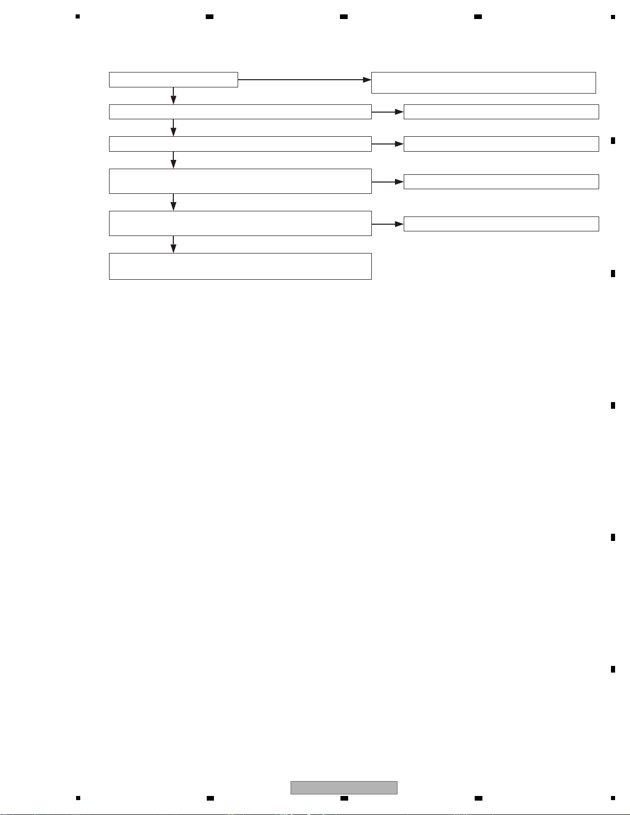
5
No sound from speakers and Preout in EXT STEREO
No sound in plural channels
Check the broken point (start with checking the
relevant channel of CN2003)
Check of power source: Is there ±12V in CN2004 ?
Check of power source: Is there ±6V in CN2004 ?
Check the circuit of the connection destination.
Check the circuit of the connection destination.
Check the circuit of the connection destination.
No sound only in analog input
Check the peripheral circuit of IC2027.
No sound only in COAX input or OPT input
Check the peripheral circuit of IC2003.
No sound only from ZONE 2 of FRONT USB
Check the peripheral circuit of IC2026.
No
No
No
No
No
Yes
Yes
Yes
Yes
Yes
Check the peripheral circuit of X2001.
The signal(DABCK, DALRCK, each DATA) of the relevant
channel exist in CN2001.
80MHz clock exist in 19pins of IC2009 and IC2010.
Check the broken point (start with checking the relevant
channel of CN2003), and check the peripheral circuit.
No sound only in BT
Check the 14, 16pin of JA2010, the power source and control signals.
DAC HIGH ASSY DIGNOSIS
6 7 8
A
B
C
D
E
5
SC-95
6 7 8
F
27
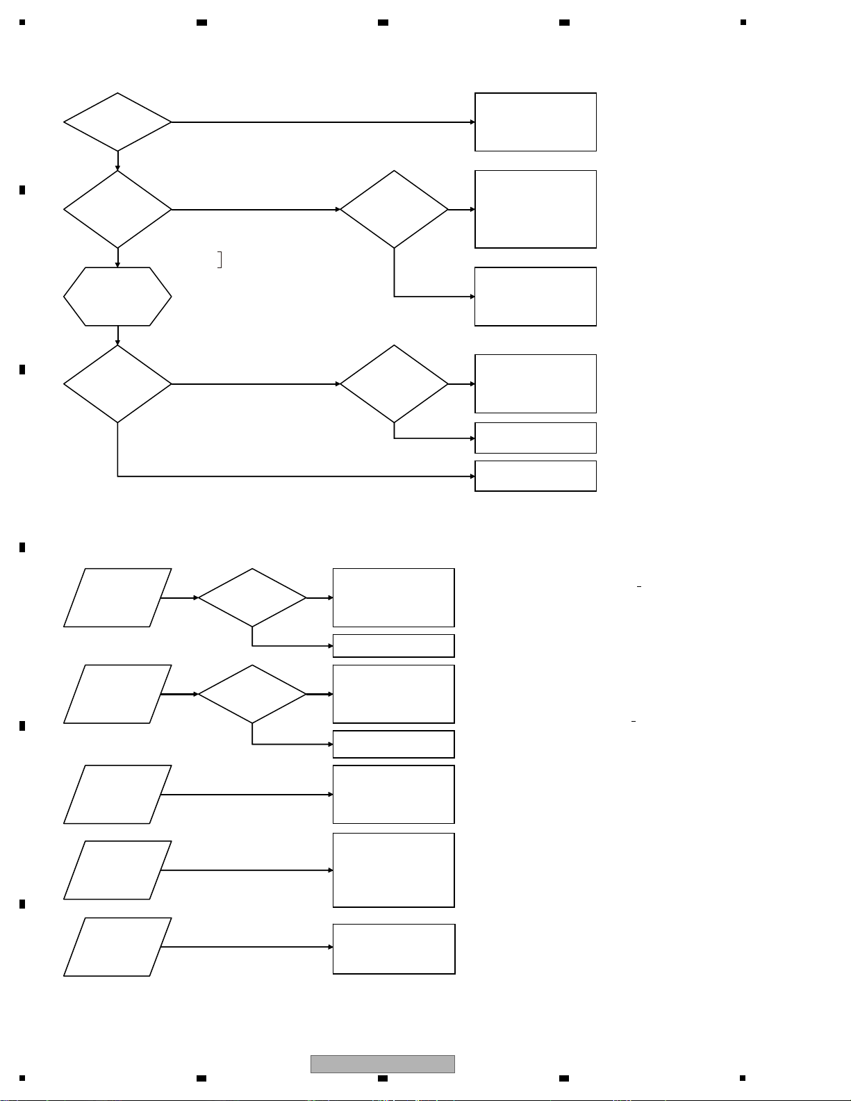
1
1) No Sound
No
Yes
No
No
Yes
Yes
No
No
Yes
Yes
NOTE : Wiring number listed is the example of Front L-ch
2) Diagnosis Flow Chart from Error Symptom
Failure locating method from error symptom is available as diagnosis after product shutdown.
Diagnosis Flow Chart from error symptom due to Amplifier Section is shown here.
Cause of being BERR
When B-Power Supply Voltage exceeds
+
75 V
No
When B-Power Supply Voltage falls below +20 V
Yes
Cause of being OL
No
At Over Current Detected (Not worked with no-load)
At Driver IC not Oscillated
At ZOBEL Detection Circuit Activated
Yes
Cause of being DC
When DC 7V or above is output in Audio Output Line
Cause of being TEMPERR
When MOSFET Temperature exceeds approx. 120 degrees
When MOSFET temperature is suddenly increased
Shorted MOSFET (Q4101, Q4102)
Failure BERR Detection Circuit
(around Q4022, Q4024)
Check Connector Conductivity
Oscillation
Waveform on Driver IC
(IC4101) Output (13pin) seen
just in a moment
at restarting?
Parts Failure after AMPLPF
(L4100, C4101)
Failure in MOSFET (Q4101, Q4102)
Check Power Supply on
Temperature Detection Circuit
(around R4181 and Q4117)
Perform impedance check on
Audio Output Line vs. Power Supply
Failure around Driver ->
Replace Driver IC
Failure around ZOBEL Detection
Circuit (Q4104, etc)
Power
Distribution
Status
Any Switching
Residual Waveform existed
in Speaker Output* ?
(Sine wave = Approx.
450 KHz, 0.7V rms)
Audio Signal Input
Check how far the
signal is passing
MUTE cleared ?
Check MUTE Control
voltage (Q4109 Base)
V = -12V (Normally)
Go to 2) Diagnosis Flow Chart
from Error Symptom if immediate
shut down happens by the
Protection Circuit.
Check LPF COIL Conductivity
(L4100)
Check each Power Supply of
Driver IC (IC4101)
Check Relay (RY4100) is ON
Check MUTE Control Line
Signal exists just
before Driver IC (IC4101) ?
Check the four block ASSY of
D AMP_SS(_S) ASSY
Failure Driver IC (IC4101)
Abnormality
Detection on
AMP Power
Voltage (BERR)
Over Current
Detection (OL)
DC Detection
TEMPERR
Check XBERR Line Conductivity
from D AMP_SS(_S) ASSY
CN4000-6pin to DISPLAY ASSY
CN6001-31pin.
BERR Conductivity
Failure Detection
(CERR)
Approx. DC 2V
exists in
Speaker Output ?
Check Voltage of Driver IC
CSD Port (5pin)
DIGITAL AMP BLOCK FLOWCHART
(Waveform 1 and 2)*
* : Refer to D AMP_SS(_S) ASSY (2/6)
There is a problem
in Conduction of Power
Supply Connector* ?
*: (CN4001, CN4002,
CN4003, CN4004)
*
Precautions for checking the speaker output
For the channel shown below, positive and negative of
SP terminal are inverted.
surround ch :
surround back ch :
The black terminal is HOT
and the red terminal is ground.
Parts Failure after AMPLPF (L4100, Q4101)
A
2 3 4
B
C
D
E
F
28
1
2 3 4
SC-95
5
No Picture
Analog Video IN ?
Diagnose or replace
FRONT HDMI USB ASSY
Composite in
Composite out ?
Check
COMPONENT ASSY
CN8303 video signals
Diagnose COMPONENT ASSY
(around IC8301)
or replace COMPONENT ASSY
Diagnose COMPOSITE ASSY
(input circuits)
or replace COMPOSITE ASSY
Diagnose COMPOSITE ASSY
(output circuits)
or replace COMPOSITE ASSY
Component in
Component out ?
Front HDMI in
HDMI out ?
Diagnose or replace
DIGITAL MAIN ASSY
Composite
(Component) in
HDMI out ?
Diagnose or replace
DIGITAL MAIN ASSY
No GUI ?
HOME MENU GUI
USB GUI
NETWORK GUI
Diagnose DIGITAL MAIN ASSY
(around IC1602)
or Replace DIGITAL MAIN ASSY
No Problem
IN:NG,
OUT:NG
IN:OK,OUT:OK
IN:OK,
OUT:NG
HDMI IN3,IN4, IN6 and IN7
HDMI out ?
NG
OK
Check connection
(FRONT HDMI USB ASSY
DIGITAL MAIN ASSY)
Rear HDMI in
HDMI out ?
Diagnose or replace
DIGITAL MAIN ASSY
Check
DIGITAL MAIN ASSY
CN901 video signals
ONLY GUI ?
Replace Network Module (AXX7293)
NO
YES
This is just for general reference and does not including every single case.
In case of using 4K/60p-compatible TV and no picure.
The receiver’s HDMI input terminals support the 4K/60p signal. However, there are two types of terminals as follows.
Type 1: 4K/60p 4:4:4 24 bit signal (transmission speed up to 18 Gbps) can be transmitted: BD, DVD (HDMI IN 1), SAT (HDMI IN 2)
Type 2: 4K/60p 4:2:0 24 bit signal can be transmitted (4K/60p 4:4:4 24 bit signal is not supported, transmission speed up to 10.2 Gbps):
HDMI input terminals other than the above
NOTE: All input terminals are type 2 when HDZONE is turned on.
1. When a source device that does not support the 4K/60p 4:4:4 24 bit signal is connected to a type 1 terminal, the video image may become reddish,
sound may not be output, or 3D signals may not be output for some devices. For such devices, try the following.
*This is not a malfunction of the receiver.
Connect the device to a type 2 terminal instead of the type 1 terminal.
It is also possible to set all input terminals to type 2. Set the following “HDMI 4K/60p signal output setting” to “4:2:0”.
2. When the video image is not output, is interrupted, or there is noise, the cause may be the HDMI cable. (Some HDMI cables do not support
4K/60p 4:4:4 24 bit signal transmission.) In such cases, set the following “HDMI 4K/60p signal output setting” to “4:2:0”.
HDMI 4K/60p signal output setting
Operation is performed on the front panel of the unit. You cannot perform the setting if the multizone function is not set to MULTI ZONE OFF.
1 Switch the receiver into standby.
2 While holding down ENTER on the front panel, press STANDBY/ON.
The display shows RESET NO .
3 Use / to select ‘4K/60p’.
4 Use / to select the signal to set.
4:4:4 – Select this setting when connecting to a 4K/60p 4:4:4 24 bit compatible TV using HDMI. More high quality video images can be enjoyed.
4:2:0 – Select this setting when connecting to a 4K/60p 4:2:0 24 bit compatible TV using HDMI.
5 When you’re finished, press RETURN.
6 Press STANDBY/ON to switch on the receiver and your TV.
Make sure that the TV’s video input is set to this receiver.
6 7 8
NO PICTURE
A
B
C
D
5
6 7 8
SC-95
E
F
29
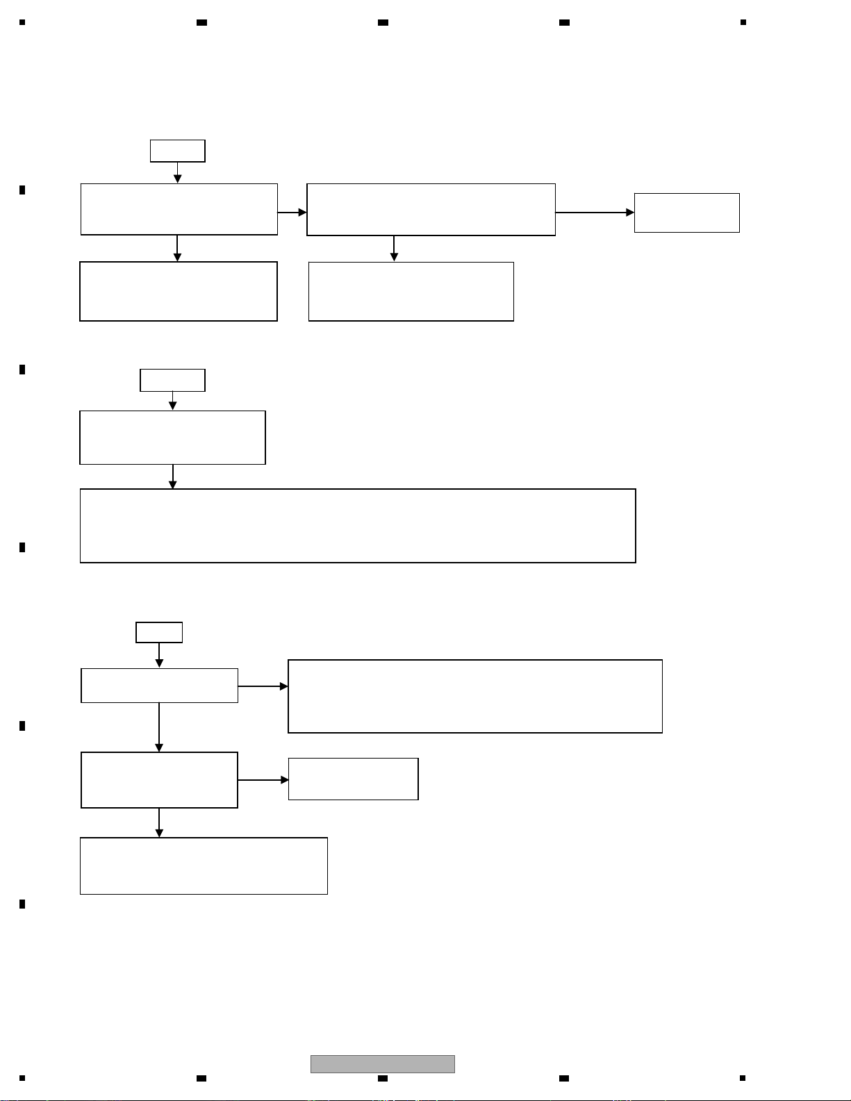
1
This is just for general reference and does not including every single case.
12V Trig
RS-232C
IR
IR
RS-232C
Remote Control
No
Yes
No
No
Still NG
NG
Repair or replace
NG point
No Problem
12V Trig
Check INTERFACE_S ASSY
CN7011 or CN7012 18pin +12V
No
Yes
No
Check the power supply path of V+12_TRG
V-REG_S ASSYINTERFACE_S ASSY
ALL NG
Other results
Repair or replace
NG point
Check the signal path of 232RX,232TX,232POW,232CDET
COMPONENT ASSY DIGITAL MAIN ASSY V-REG_S ASSY DISPLAY ASSY(IC6001)
and check the power supply path of V+5R6_EV
PRIMARY ASSY DIGITAL MAIN ASSY COMPONENT ASSY
Diagnose INTERFACE_S ASSY
(Circuits around Q7008,Q7010)
or replace INTERFACE_S ASSY
Diagnose COMPONENT ASSY
(around IC8601)
or replace COMPONENT ASSY
Diagnose INTERFACE_S ASSY(IR circuits)
or check the signal path of IR-IN
INTERFACE_S ASSY V-REG_S ASSY DISPLAY ASSY
or replace INTERFACE_S ASSY
Check the signal path of
RMC
DISPLAY ASSY
Diagnose DISPLAY ASSY
(RMC signal path, around U6001,IC6001)
or replace DISPLAY ASSY
Diagnose V-REG_S ASSY
(Circuits around IC7551)
or replace V-REG_S ASSY
2 3 4
OTHER
A
B
C
D
E
F
30
1
SC-95
2 3 4
Loading...