

Page 1
ORDER NO.
CRT3466
AVIC-D1/UC
DOUBLE-DIN DVD NAVIGATION SYSTEM
AVIC-D1
This service manual should be used together with the following manual(s):
Model No. Order No. Mech.Module Remarks
CX-3016 CRT3056 MS3 DVD Mech. Module:Circuit Description, Mech. Description, Disassembly
CX-3158 CRT3394 S10.1AAC CD Mech. Module:Circuit Description, Mech. Description, Disassembly
This product has the unit part number as below.
Unit Part No.
CPN1951
*) The unit part numbers listed above are not for the service components.
Description
Navigation Unit
/UC
For details, refer to "Important Check Points for Good Servicing".
PIONEER CORPORATION 4-1, Meguro 1-chome, Meguro-ku, Tokyo 153-8654, Japan
PIONEER ELECTRONICS (USA) INC. P.O. Box 1760, Long Beach, CA 90801-1760, U.S.A.
PIONEER EUROPE NV Haven 1087, Keetberglaan 1, 9120 Melsele, Belgium
PIONEER ELECTRONICS ASIACENTRE PTE. LTD. 253 Alexandra Road, #04-01, Singapore 159936
PIONEER CORPORATION 2005
K-ZZW. APR. 2005 Printed in Japan
Page 2
CAUTIO
e
r
ect
thend
d
the
to
the
d
g
to
ARNING
This
tains
d
tai
ical
tai
icals
hich
to
the
5
g
1234
SAFETY INFORMATION
A
This service manual is intended for qualified service technicians; it is not meant for the casual do-it-yourself
Qualified technicians have the necessary test equipment and tools, and have been trained to properly and safely repai
erformed
ou
renotualified
ARNING
roduct
Health & Safety Code Section 25249.6 - Proposition 6
B
This product contains mercury. Disposal of this material may be regulated due to environmental considerations.
For disposal or recyclin
Alliance: www.eiae.org.
n
information, please contact your local authorities or the Electronics Industries
n adversely
repair
r
n
ff
thisroduct
n
reliability theroduct
roperlyn
r
arts
n
n
ou
m
ndmayvoi
houldnotrisktryin
w
r
nown
- Service Precautions
1. You should conform to the regulations governing the product (safety, radio and noise, and other regulations),
and should keep the safety during servicing by following the safety instructions described in this manual.
C
D
DVD MECHANISM MODULE section precaution
1. EJECT LOCK MODE for DVD mechanism
In order to enter "EJECT LOCK" mode, reset start while pressing the "AV" and "INFO" keys together.
Pressing the "AV" and "INFO" keys until monitor backlight is turned on.
In order to exit "EJECT LOCK" mode, follow the same steps to enter this mode.
2. Before disassembling the unit, be sure to turn off the power. Unplugging and plugging the connectors
during power-on mode may damage the ICs inside the unit.
3. To protect the pickup unit from electrostatic discharge during servicing, take an appropriate treatment
(shorting-solder) by referring to "the DISASSEMBLY" .
4. After replacing the pickup unit, be sure to skew adjustment.
5. During disassembly, be sure to turn the power off since an internal IC might be destroyed when a connector
is plugged or unplugged.
CD MECHANISM MODULE section precaution
1. Before disassembling the unit, be sure to turn off the power. Unplugging and plugging the connectors
during power-on mode may damage the ICs inside the unit.
2. To protect the pickup unit from electrostatic discharge during servicing, take an appropriate treatment
(shorting-solder) by referring to "the DISASSEMBLY".
3. After replacing the pickup unit, be sure to check the grating.
E
F
is a trademark of DVD Format/Logo Licensing Corporation.
2
1234
AVIC-D1/UC
Page 3
5678
[Important Check Points for Good Servicing]
In this manual, procedures that must be performed during repairs are marked with the below symbol.
Please be sure to confirm and follow these procedures.
1. Product safety
Please conform to product regulations (such as safety and radiation regulations), and maintain a safe servicing environment by
following the safety instructions described in this manual.
1 Use specified parts for repair.
Use genuine parts. Be sure to use important parts for safety.
2 Do not perform modifications without proper instructions.
Please follow the specified safety methods when modification(addition/change of parts) is required due to interferences such as
radio/TV interference and foreign noise.
3 Make sure the soldering of repaired locations is properly performed.
When you solder while repairing, please be sure that there are no cold solder and other debris.
Soldering should be finished with the proper quantity. (Refer to the example)
4 Make sure the screws are tightly fastened.
Please be sure that all screws are fastened, and that there are no loose screws.
5 Make sure each connectors are correctly inserted.
Please be sure that all connectors are inserted, and that there are no imperfect insertion.
6 Make sure the wiring cables are set to their original state.
Please replace the wiring and cables to the original state after repairs.
In addition, be sure that there are no pinched wires, etc.
7 Make sure screws and soldering scraps do not remain inside the product.
Please check that neither solder debris nor screws remain inside the product.
8 There should be no semi-broken wires, scratches, melting, etc. on the coating of the power cord.
Damaged power cords may lead to fire accidents, so please be sure that there are no damages.
If you find a damaged power cord, please exchange it with a suitable one.
9 There should be no spark traces or similar marks on the power plug.
When spark traces or similar marks are found on the power supply plug, please check the connection and advise on secure
connections and suitable usage. Please exchange the power cord if necessary.
0 Safe environment should be secured during servicing.
When you perform repairs, please pay attention to static electricity, furniture, household articles, etc. in order to prevent injuries.
Please pay attention to your surroundings and repair safely.
A
B
C
D
2. Adjustments
To keep the original performance of the products, optimum adjustments and confirmation of characteristics within specification.
Adjustments should be performed in accordance with the procedures/instructions described in this manual.
3. Lubricants, Glues, and Replacement parts
Use grease and adhesives that are equal to the specified substance.
Make sure the proper amount is applied.
4. Cleaning
For parts that require cleaning, such as optical pickups, tape deck heads, lenses and mirrors used in projection monitors, proper
cleaning should be performed to restore their performances.
5. Shipping mode and Shipping screws
To protect products from damages or failures during transit, the shipping mode should be set or the shipping screws should be
installed before shipment. Please be sure to follow this method especially if it is specified in this manual.
56
AVIC-D1/UC
E
F
7
8
3
Page 4

1234
CONTENTS
SAFETY INFORMATION.....................................................................................................................................2
1. SPECIFICATIONS ............................................................................................................................................ 5
2. EXPLODED VIEWS AND PARTS LIST............................................................................................................ 8
A
B
C
D
E
F
2.1 PACKING ................................................................................................................................................... 8
2.2 EXTERIOR (1) ......................................................................................................................................... 10
2.3 EXTERIOR (2) ......................................................................................................................................... 12
2.4 EXTERIOR (3) ......................................................................................................................................... 14
2.5 DVD MECHANISM MODULE(MS3).........................................................................................................16
2.6 CD MECHANISM MODULE(S10.1AACA)............................................................................................... 18
3. BLOCK DIAGRAM AND SCHEMATIC DIAGRAM..........................................................................................20
3.1 BLOCK DIAGRAM................................................................................................................................... 20
3.2 OVERALL CONNECTION DIAGRAM...................................................................................................... 32
3.3 CC UNIT (P/S) ......................................................................................................................................... 34
3.4 CC UNIT (CPU, ASIC, SDRAM)(GUIDE PAGE)......................................................................................36
3.5 CC UNIT (GRAPHIC)(GUIDE PAGE) ...................................................................................................... 42
3.6 CC UNIT (ROM, SRAM, BUS-BUFFER) ................................................................................................. 48
3.7 CC UNIT (MAIN, CC CORE I/F) .............................................................................................................. 50
3.8 CC UNIT (GPS, SENSOR, VIDEO, I/F) ................................................................................................... 52
3.9 GPS UNIT (GUIDE PAGE)....................................................................................................................... 58
3.10 DVD CORE UNIT(MS3R)(GUIDE PAGE) .............................................................................................. 64
3.11 COMPOUND UNIT(A) AND COMPOUND UNIT(B) .............................................................................. 72
3.12 PU UNIT(REFERENCE)........................................................................................................................ 73
3.13 CD MECHANISM MODULE(GUIDE PAGE)..........................................................................................74
3.14 SYSTEM UNIT (AUDIO)........................................................................................................................ 84
3.15 SYSTEM UNIT (SYSCOM, VIDEO, I/F)(GUIDE PAGE).........................................................................86
3.16 SYSTEM UNIT (P/S).............................................................................................................................. 92
3.17 MONITOR PCB (GUIDE PAGE)............................................................................................................. 94
3.18 KEYBOARD PCB................................................................................................................................. 102
3.19 PANEL PCB ......................................................................................................................................... 104
3.20 CONNECTOR UNIT.............................................................................................................................106
3.21 MAIN PCB UNIT .................................................................................................................................. 108
4. PCB CONNECTION DIAGRAM ...................................................................................................................110
4.1 CC UNIT.................................................................................................................................................110
4.2 GPS UNIT.............................................................................................................................................. 114
4.3 DVD CORE UNIT(MS3R).......................................................................................................................116
4.4 COMPOUND UNIT(A) AND COMPOUND UNIT(B) .............................................................................. 120
4.5 CD CORE UNIT(S10.1) ......................................................................................................................... 122
4.6 SYSTEM UNIT.......................................................................................................................................124
4.7 MONITOR PCB...................................................................................................................................... 128
4.8 KEYBOARD PCB................................................................................................................................... 132
4.9 PANEL PCB ........................................................................................................................................... 134
4.10 CONNECTOR UNIT.............................................................................................................................136
4.11 MAIN PCB UNIT .................................................................................................................................. 138
5. ELECTRICAL PARTS LIST ..........................................................................................................................140
6. ADJUSTMENT ............................................................................................................................................. 166
6.1 JIG CONNECTION DIAGRAM...............................................................................................................166
6.2 DVD ADJUSTMENT...............................................................................................................................167
6.3 CD ADJUSTMENT................................................................................................................................. 172
6.4 CHECKING THE GRATING AFTER CHANGING THE PICKUP UNIT.................................................. 174
6.5 ERROR MODE ...................................................................................................................................... 176
6.6 MONITOR PCB ADJUSTMENT.............................................................................................................177
6.7 TEST MODE .......................................................................................................................................... 186
6.8 USING THE TEST DISC........................................................................................................................ 209
7. GENERAL INFORMATION........................................................................................................................... 221
7.1 DIAGNOSIS........................................................................................................................................... 221
7.1.1 DISASSEMBLY ................................................................................................................................... 221
7.1.2 PCB LOCATIONS ............................................................................................................................... 231
7.1.3 CONNECTOR FUNCTION DESCRIPTION........................................................................................ 232
7.2 IC ...........................................................................................................................................................233
7.3 EXPLANATION ...................................................................................................................................... 258
7.3.1 MECHANISM DESCRIPTIONS.......................................................................................................... 258
7.3.2 OPERATIONAL FLOW CHART.......................................................................................................... 264
8. OPERATIONS .............................................................................................................................................. 266
4
1234
AVIC-D1/UC
Page 5

5678
1. SPECIFICATIONS
General
Rated power source............14.4 V DC
Grounding system...............Negative type
Max. current consumption
...................................10.0 A
Backup current...................3.0 mA or less
Navigation unit:
Dimensions (W x H x D):
DIN
Chassis.................178 x 100 x 160 mm
Nose......................191 x 114 x 5 mm
D
Chassis.................178 x 100 x 165 mm
Nose......................171 x 93 x 24 mm
Weight..........................2.9 kg (6.4 lbs)
Navigation
GPS Receiver:
System..........................L1, C/Acode GPS
SPS (Standard Positioning Service)
Reception system........8-channel multi-channel
Reception frequency...1,575.42 MHz
Sensitivity.....................–130 dBm
Position update frequency
...................................Approx. once per second
GPS antenna:
Antenna........................Micro strip flat antenna/
Antenna cable.............. 5.0 m (16 ft. 5 in.)
Dimensions (W x H x D)
...................................33 x 13 x 36 mm
Weight..........................105 g(0.23 lbs)
Display
Screen size/aspect ratio.....6.5 inch wide/16:9
Pixels.................................... 336,960 (1,440 x 234)
Type...................................... TFT active matrix, transmis-
Color system........................ NTSC
Operating temperature range
...........................................–14 – +122
Storage temperature range
...........................................–4 – +176
Angle adjustment.................. 0 – 21°
(10.8 - 15.1 V allowable)
(7 x 3-7/8 x 6-1/4 in.)
(7-1/2 x 4-1/2 x 1/4 in.)
(7 x 3-7/8 x 6-1/2 in.)
(6-3/4 x 3-5/8 x 1 in.)
reception system
right-handed helical polarization
(1-1/4 x 1/2 x 1-3/8 in.)
(effective display area: 144 x
76 mm)
sive type
(initial settings: 0°)
°F
°F
Audio
Continuous power output is 22 W per channel minimum
into 4 ohms, both channels driven 50 to 15,000 Hz with
no more than 5% THD.
Maximum power output......50 W x
Load impedance...................4 Ω (4 – 8 Ω [2 Ω for 1 ch]
Preout max output level/output impedance
............................................2.0 V/100 ohm
Equalizer (3-Band Parametric Equalizer):
Low
Frequency.............. 40/80/100/160 Hz
Q Factor..................0.35/0.59/0.95/1.15 (+6 dB
Gain....................... ±12dB
Mid
Frequency..............200/500/1k/2k Hz
Q Factor..................0.35/0.59/0.95/1.15 (+6 dB
Gain.......................±12dB
High
Frequency............. 3.15k/8k/10k/12.5k Hz
Q Factor................. 0.35/0.59/0.95/1.15 (+6 dB
Gain.......................±12dB
Loudness contour
Low................................+3.5 dB (100 Hz), +3 dB (10
Mid.................................+10 dB (100 Hz), +6.5 dB
High....................... +11 dB (100 Hz), +11 dB
HPF:
Frequency..................... 50/80/125 Hz
Slope.............................. –12 dB/oct
Subwoofer:
Frequency..................... 50/80/125 Hz
Slope..............................–18 dB/oct
Gain...............................±12dB
Phase............................Normal/Reverse
CD Drive
System...................................Compact disc audio system
Usable discs..........................Compact disc
Signal format:
Sampling frequency.....44.1 kHz
Number of quantization bits
....................................16; linear
Frequency characteristics...5 – 20,000 Hz (±1 dB)
Signal-to-noise ratio............. 94 dB (1 kHz) (IHF-A net-
Dynamic range.....................92 dB (1 kHz)
Number of channels............2 (stereo)
MP3 decoding format..........MPEG-1 & 2 Audio Layer 3
WMA decoding format........Ver 7, 7.1, 8, 9 (2ch audio)
Wave signal format..............Linear-PCM, MS ADPCM
FM tuner
Frequency range..................87.9 – 107.9 MHz
4
50 W x 2 ch/4 Ω+ 70 W x 1
ch/2 Ω (for subwoofer)
allowable)
when boosted)
when boosted)
when boosted)
kHz)
(10 kHz)
(10 kHz)
(volume: –30 dB)
work)
A
B
C
D
E
56
AVIC-D1/UC
F
7
8
5
Page 6

1234
Usable sensitivity.................. 8 dBf (0.7 µV/75 Ω, mono, S/
A
B
50 dB quieting sensitivity.......10 dBf (0.9 µV/75 Ω, mono)
Signal-to-noise ratio.............. 75 dB (IHF-A network)
Distortion.............................. 0.3 % (at 65 dBf, 1 kHz,
Frequency response.............. 30 – 15,000 Hz (±3 dB)
Stereo separation..................45 dB (at 65 dBf, 1 kHz)
Selectivity..............................80 dB (±200 kHz)
Three-signal intermodulation (desired signal level)
.......................................... 30 dBf (two undesired signal
AM tuner
Frequency range..................530 – 1,710 kHz (10 kHz)
Usable sensitivity.................18 µV (S/N: 20 dB)
Signal-to-noise ratio............. 65 dB (IHF-A network)
N: 30 dB)
stereo)
0.1 % (at 65 dBf, 1 kHz,
mono)
level: 100 dBf)
Note:
• Specifications and the design are subject to
possible modifications without notice due to
improvements.
C
D
E
F
6
1234
AVIC-D1/UC
Page 7

5678
A
B
C
D
E
56
AVIC-D1/UC
F
7
8
7
Page 8
N
1234
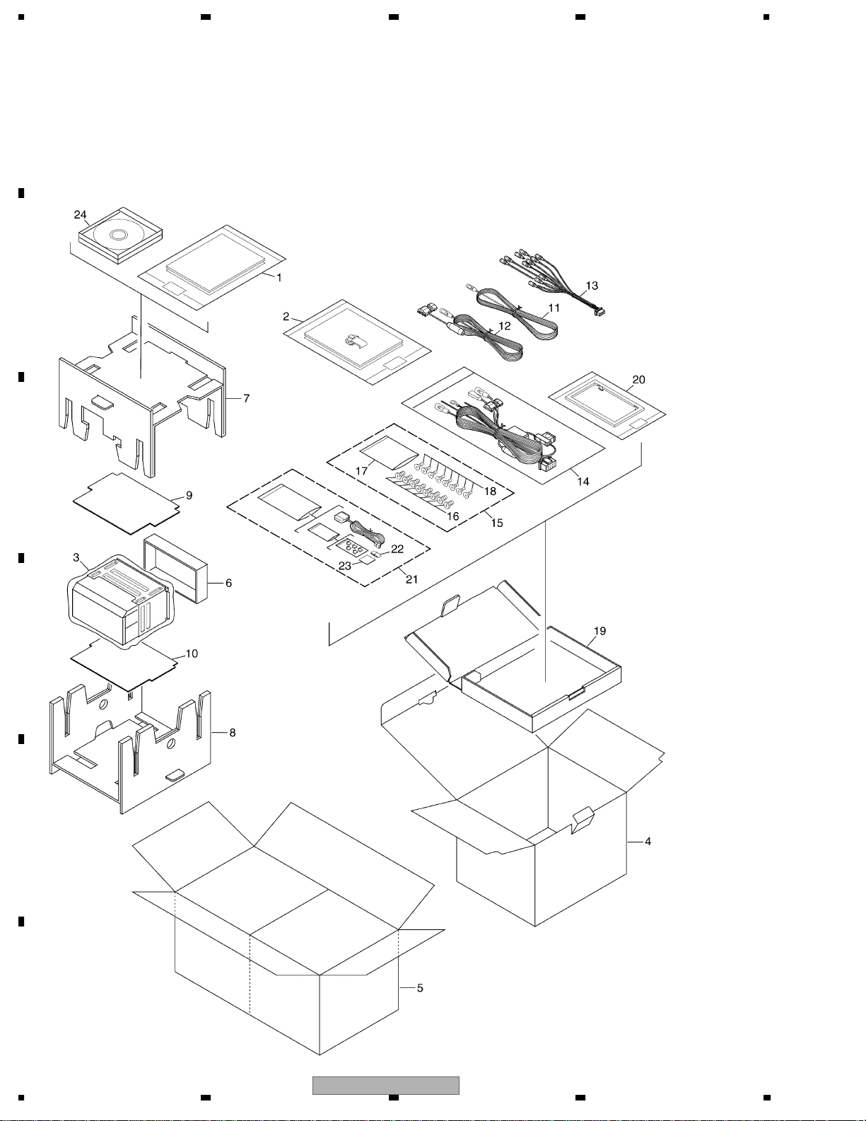
2. EXPLODED VIEWS AND PARTS LIST
OTES : • Parts marked by " * " are generally unavailable because they are not in our Master Spare Parts List.
• The > mark found on some component parts indicates the importance of the safety factor of the part.
A
Therefore, when replacing, be sure to use parts of identical designation.
• Screw adjacent to mark on the product are used for disassembly.
• For the applying amount of lobricants or glue, follow the instructions in this manual.
(In the case of no amount instructions,apply as you think it appropriate.)
2.1 PACKING
B
"
C
D
E
F
8
1234
AVIC-D1/UC
Page 9
- Owner's Manual, Installation Manual
Part No.
CRB2088, CRB2089
CRB2090, CRB2091
CRD3983
Language
English
French
English, French
- Be careful when ordering parts, as the following unit of this mainframe is described on several pages.
MONI_PANEL Unit CWM9920 MONITOR PCB
KEYBOARD PCB
PANEL PCB
Page 15 No. 18(1/2)
Page 15 No. 18(2/2)
Page 11 No. 58
Description Part No. PCB name
Reference page and No.
5678
PACKING SECTION PARTS LIST
Mark No. Description Part No.
* 1-1 Card ARY1048
1-2 Caution Card CRP1310
* 1-3 Registration Card CRY1238
1-4 Polyethylene Bag CEG1116
1-5 Owner's Manual/POC/FRE CRB2091
1-6 Owner's Manual/POC/FRE CRB2090
2-1 Owner's Manual CRB2088
2-2 Owner's Manual CRB2089
2-3 Installation Manual CRD3983
2-4 Connector CKX1049
A
2-5 Polyethylene Bag CEG1116
3 Cover CEG1359
4 Carton CHG5523
5 Contain Box CHL5523
6 Protector CHP2273
7 Protector CHP3006
8 Protector CHP3007
9 Protector CHP3045
10 Protector CHP3046
11 Cord CDE5044
12 Cord CDE6825
13 Cord Assy CDE7838
14 Cord Assy CDE7839
15 Screw Assy CEA3797
16 Screw BMZ50P060FTC
* 17 Polyethylene Bag CEG-127
18 Screw CMZ50P060FTC
19 Sub Carton CHA3298
20 Panel CNS8298
21 GPS Antenna Assy CXC4864
22 Water Proof Pad CZN5442
23 Sheet CZN7008
24 DVD-ROM CPJ1167
B
C
D
56
AVIC-D1/UC
7
E
F
8
9
Page 10
1234
2.2 EXTERIOR (1)
A
B
C
D
E
F
10
1234
AVIC-D1/UC
Page 11

5678
EXTERIOR (1) SECTION PARTS LIST
Mark No. Description Part No.
1 Screw BMZ26P030FTB
2 Screw BMZ26P040FTC
3 Screw BMZ26P060FTB
4 Screw BMZ26P140FTC
5 Screw(M2x3) CBA1527
6 Screw(M3x10) CBA1637
7 Screw(M2x2) CBA1735
8 Screw(M2x3) CBA1877
9 Spring CBH2888
10 Cord Assy CDE7908
11 FFC CDE8006
12 FFC CDE8007
13 Cord Assy CDE8008
14 Screw CMZ50P060FTC
15 Case CNB3109
16 Cover CND1509
17 Holder CND2682
18 Holder CND2683
19 Shield CND2775
20 Holder CND2794
21 Bracket CND2795
22 Insulator CNM8550
23 Insulator CNM9442
24 Gasket CNM9593
25 Cushion CNM9653
Mark No. Description Part No.
50 Holder CND2669
51 Holder CND2670
52 Holder CND2671
53 Holder CND2685
54 Button(CD EJECT) CAC9119
55 Button(DVD EJECT) CAC9120
56 Panel Unit CXC4435
57 Screw IMS26P040FTC
58 MONI_PANEL Unit CWM9920
59 Connector(CN5901) CKS4825
60 Chassis Unit CXC4333
61
62 DVD Mechanism Module(MS3) CXK6333
63 Fan Motor CXM1320
64 Screw ISS26P055FTC
65 Tape CNM9890
66 IC(IC4200) PAL007B
67 Transistor(Q1900, 1902) 2SB1185
68 Transistor(Q1922) 2SD2396
CD Mechanism Module(S10.1AACA)
CXK5668
A
B
C
26 Shield CNM9656
27 Flexible PCB CNP8450
28 Heat Sink CNR1785
29 Cover CNS8290
30 System Unit CWM9918
31 Screw BMZ26P050FTC
32 FM/AM Tuner Unit CWE1646
33 Holder CND1054
34 Terminal(CN1302) CKF1064
35 Terminal(CN1303) CKF1064
36 Terminal(CN1304) CKF1064
37 Terminal(CN1305) CKF1064
38 Terminal(CN4301) CKF1064
39 Connector(CN1801) CKM1438
40 Connector(CN1401) CKM1460
41 Jack(CN1450) CKN1036
42 Connector(CN1803) CKS4822
43 Connector(CN1301) CKS4919
44 Connector(CN1651) CKS4980
45 Connector(CN1701) CKS5110
46 Connector(CN1802) CKS5270
47 Antenna Jack(CN4300) CKX1056
48 Holder CND2667
49 Holder CND2668
D
E
F
56
AVIC-D1/UC
7
8
11
Page 12
1234
2.3 EXTERIOR (2)
A
B
C
D
E
F
12
1234
AVIC-D1/UC
Page 13

5678
EXTERIOR (2) SECTION PARTS LIST
Mark No. Description Part No.
1 Drive Unit CXC4423
2 Screw(M2x6) CBA1399
3 Screw(M2x1.5) CBA1615
4 Screw(M2x2) CBA1771
5 Spring CZB3092
6 Spring CZB3093
7 Screw CZB3097
8 Washer CZB5003
9 Shaft CZL3010
10 Gear CZN7011
11 Gear CZN7012
12 Gear CZN7013
13 Rack CZN7014
14 Holder CZN7015
15 Roller CZN7052
16 Holder CZN7042
17 Holder CZN7043
18 Sheet CZN7044
19 Main PCB Unit CZW3097
20 Screw BMZ26P050FTC
21 Connector(CN2) CKS4600
22 Heat Sink CND1228
23 Connector(CN1) CZK3071
24 Transistor(Q1) 2SB1185
25 Bracket Unit CZX5101
Mark No. Description Part No.
50 Insulator CNM9438
51 Insulator CNM9439
52 GPS Unit CWX3141
53 Connector(CN461) CKS4280
54 Connector(CN504) CKS4432
55 Shield CNC9191
56 Shield CNC9192
57 Holder CND1535
58 Connector(CN2) DKN1236
59 Connector Unit CWM9921
60 Terminal(CN2807) CKF1064
61 Connector(CN2802) CKS3414
62 Connector(CN2801) CKS4590
63 Connector(CN2806) CKS4600
64 Connector(CN2804) CKS5209
65 Holder(CN58) CNC2218
66 Holder CND2673
67 FFC CDE7864
68 FFC CDE8005
69 Screw ISS26P055FTC
70 •••••
71 Cushion CNM9416
A
B
C
26 Motor Unit(FLAP)(M10) CZX5102
27 Chassis Unit CZX5127
28 Frame Unit CZX5160
29 Screw JFZ20P020FTC
30 Washer YE15S
31 CC Unit CWM9919
32 Terminal(CN100) CKF1064
33 Terminal(CN601) CKF1064
34 Terminal(CN602) CKF1064
35 Terminal(CN802) CKF1064
36 Connector(CN701) CKS3805
37 Connector(CN702) CKS3991
38 Connector(CN551) CKS4065
39 Connector(CN651) CKS4473
40 Connector(CN801) CKS4674
41 Connector(CN605) CKS5110
42 Holder CND2672
43 Shield CND2675
44 Shield CND2676
45 Shield CND2679
46 Shield CND2680
47 Sheet CNM6903
48 Insulator CNM9436
49 Insulator CNM9437
D
E
F
56
AVIC-D1/UC
7
8
13
Page 14
1234
2.4 EXTERIOR (3)
A
B
C
D
E
F
14
1234
AVIC-D1/UC
Page 15

5678
EXTERIOR (3) SECTION PARTS LIST
Mark No. Description Part No.
1 Button(MAP, AV) CAC9112
2 Button(OPEN, ANGLE) CAC9114
3 Button(TRFC) CAC9115
4 Button(P.ADJ, MEMO) CAC9118
5 Button(SRC) CAC9429
6 Screw(M2x3) CBA1877
7 FFC CDE8003
8 Insulator CNM9475
9 Cover CNM9655
10 Guide CNV5169
A
11 Touch Panel CSX1085
12 Screw(M2x2) CBA1771
13 Holder CNC9991
14 Holder CND3075
15 Insulator CNM9567
16 Insulator CNM9803
17 Flexible PCB CNP8744
18 MONI_PANEL Unit CWM9920
19 Terminal(CN5003) CKF1064
20 Connector(CN5002) CKS3968
21 Connector(CN5801) CKS3991
22 Connector(CN5700) CKS4130
23 Connector(CN5331) CKS4428
24 Connector(CN5009) CKS4496
25 Connector(CN5007) CKS4675
26 Connector(CN5008) CKS5208
27 LCD Panel CWX3229
28 Screw PMB20P040FTC
29 Knob Unit CXC4417
30 Grille Unit CXC4434
31 Case Unit CXC4436
32 Sheet CNM9862
33 Button Unit(VOL) CXC4455
34 Button Unit(DEST, INFO) CXC4456
35 Cord CDE6825
B
C
D
36 Cap CNS1472
37 Resistor RS1/2PMF102J
38 Cord Assy CDE7838
39 Cap CNV6727
40 Cord Assy CDE7839
> 41 Fuse(10A) CEK1136
42 Cap CNS1472
43 Shield CNM9858
56
AVIC-D1/UC
E
F
7
8
15
Page 16
1234
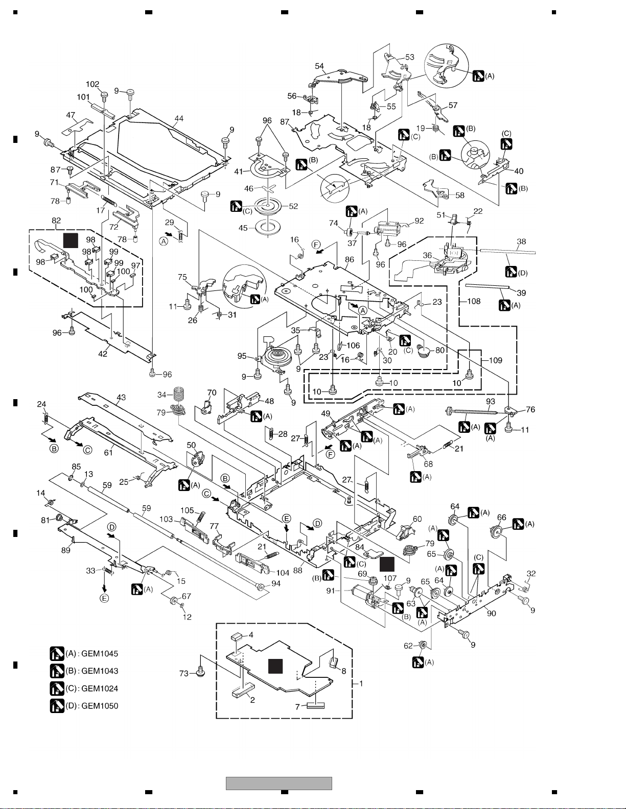
2.5 DVD MECHANISM MODULE(MS3)
A
B
D
C
D
E
E
C
F
16
1234
AVIC-D1/UC
Page 17

5678
DVD MECHANISM MODULE(MS3) SECTION PARTS LIST
Mark No. Description Part No.
1 DVD Core Unit(MS3R) CWX3178
2 Connector(CN601) CKS5055
3 •••••
4 Connector(CN1202) CKS5017
5 •••••
6 •••••
7 Connector(CN1101) CKS4842
8 Connector(CN1201) CKS5043
9 Screw BMZ20P020FTC
10 Screw(M2 x 3.5) CBA1571
11 Screw(M2 x 2.5) CBA1623
12 Washer CBF1038
13 Washer CBF1064
14 Spring CBH2586
15 Spring CBH2587
16 Spring CBH2588
17 Spring CBH2589
18 Spring CBH2590
19 Spring CBH2591
20 Spring CBH2592
21 Spring CBH2593
22 Spring CBH2594
23 Spring CBH2595
24 Spring CBH2596
25 Spring CBH2597
26 Spring CBH2598
27 Spring CBH2599
28 Spring CBH2600
29 Spring CBH2601
30 Spring CBH2602
31 Spring CBH2603
32 Spring CBH2604
33 Spring CBH2605
34 Spring CBH2711
35 Spring CBL1564
36 Pickup Unit(Service) CXX1640
37 Shaft CLA3881
38 Shaft CLA4206
39 Shaft CLA4207
40 Lever CNC9933
41 Holder CNC9939
42 Holder CND2251
43 Holder CNC9941
44 Frame CND2250
45 Sheet CNM6883
46 Sheet CNM8283
47 Sheet CNM8643
48 Lever CNV8076
49 Lever CNV7155
50 Cam CNV7156
51 Rack CNV7157
52 Clamper CNV7158
53 Arm CNV7159
54 Arm CNV7160
55 Arm CNV7161
No. Description Part No.
Mark
56 Arm CNV7162
* 57 Arm CNV7163
58 Arm CNV7164
59 Roller CNV7165
60 Arm CNV7166
61 Guide CNV8093
62 Gear CNV7169
63 Gear CNV7170
64 Gear CNV7171
65 Gear(Black) CNV7172
66 Gear CNV7173
67 Gear CNV7174
68 Rack CNV7175
69 Gear CNV7176
70 Arm CNV8077
71 Lever CNV7178
72 Lever CNV7179
73 Screw IMS20P030FTC
74 Gear CNV7181
75 Holder CNV7183
76 Holder CNV7184
77 Guide CNV7745
78 Roller CNV7344
79 Damper CNV7470
80 Damper CNV7471
81 Collar CNV7645
82 Compound Unit(A) CWX3154
83 Screw(M1.4x1.4) CBA1787
84 Compound Unit(B) CWX3156
85 Washer YE20FTC
86 Chassis Unit CXC3629
87 Arm Unit CXB8681
88 Frame Unit CXB8683
89 Arm Unit CXC4701
90 Bracket Unit CXB8685
91 Motor Unit(LOADING)(M1) CXC4659
92 Motor Unit(CARRIAGE)(M2) CXC4314
93 Screw Unit CXB8689
94 Roller Unit CXB8690
95 Motor(SPINDLE)(M3) CXM1308
96 Screw JFZ20P018FTC
97 Photo-transistor(Q1299) CPT231SCTD
98 Switch(S1201) CSN1069
99 Spring Switch(S1204) CSN1070
100 Resistor(R1298) RS1/16S0R0J
101 Guide CNV7615
102 Screw(M1.7x1.2) CBA1572
103 Arm CNV7742
104 Arm CNV7743
105 Spring CBH2710
106 Spring CBL1643
107 Spring CBH2712
108 Pickup Unit(Service)(Screw) GXX1234
109 Screw Assy CXX1750
A
B
C
D
E
F
56
AVIC-D1/UC
7
8
17
Page 18
1234
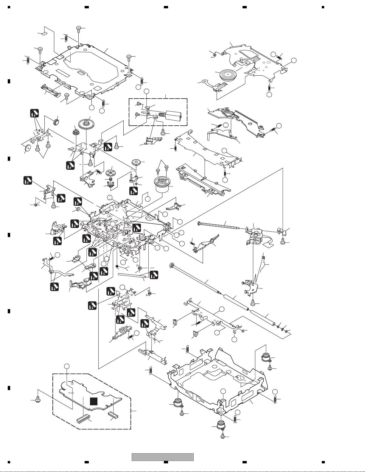
2.6 CD MECHANISM MODULE(S10.1AACA)
42
A
5
13
13
5
81
34
5
15
22
E
F
93
13
A
B
44
5
B
1
54
53
C
52
13
D
86
86
82
83
4
37
71
4
29
51
1
73
50
72
10
1
I
76
B
55
5
36
4
1
18
2
64
47
C
24
2
1
7
61
2
M
1
23
87
75
E
63
57
62
58
1
G
L
1
N
R
1
1
2
1
40
56
D
O
16
P
1
33
1
P
19
J
12
3
20
39
1
69
30
2
21
M
D
79
2
1GEM1024
2GEM1045
3GEM1035
E
92
26
G
68
28
I
H
28
45
J
38
23
K
59
49
F
Q
A
27
H
77
90
48
8
67
17
78
25
70
60
80
N
L
K
43
46
6
60
11
89
10
14
74
R
31
41
85
C
91
F
F
1
2
3
65
85
35
O
31
66
Q
14
85
18
1234
AVIC-D1/UC
Page 19

5678
CD MECHANISM MODULE(S10.1AACA) SECTION PARTS LIST
Mark No. Description Part No.
1 CD Core Unit(S10.1) CWX3096
2 Connector(CN101) CKS4182
3 Connector(CN901) CKS4017
4 Screw BMZ20P035FTC
5 Screw BSZ20P040FTC
6 Screw(M2x4) CBA1362
7 Screw(M2x3) CBA1824
8 Screw(M2x3) CBA1825
9 •••••
10 Washer CBF1038
11 Washer CBF1060
12 Spring CBH2390
13 Spring CBH2606
14 Spring CBH2607
15 Spring CBH2608
16 Spring CBH2609
17 Spring CBH2610
18 Spring CBH2735
19 Spring CBH2612
20 Spring CBH2613
21 Spring CBH2614
22 Spring CBH2615
23 Spring CBH2616
24 Spring CBH2617
25 Spring CBH2620
26 Spring CBH2621
27 Spring CBH2641
28 Spring CBH2642
29 Spring CBH2643
30 Spring CBH2659
31 Spring CBH2688
32 •••••
33 Shaft CLA4441
34 Frame CNC9962
35 Frame CNC9963
36 Bracket CND2712
37 Bracket CND1895
38 Arm CNC9968
39 Arm CND1909
40 Lever CND2032
41 Lever CNC9984
42 Sheet CNM8134
43 Collar CNV7798
44 Guide CNV7799
45 Arm CNV8403
Mark No. Description Part No.
50 Gear CNV8379
51 Gear CNV8380
52 Gear CNV8381
53 Gear CNV8382
54 Gear CNV8383
55 Gear CNV8384
56 Rack CNV8385
57 Arm CNV8386
58 Arm CNV8387
59 Guide CNV8388
60 Roller CNV7218
61 Gear CNV8389
62 Arm CNV8391
63 Arm CNV8390
64 Arm CNV8392
65 Damper CNV7313
66 Damper CNV7314
67 Arm CNV8394
68 Arm CNV8395
69 Guide CNV8396
70 Guide CNV8397
71 Holder CNV8398
72 Arm CNV8402
73 Gear CNV8400
74 Damper CNV7618
75 Motor Unit(M1) CXC4440
76 Chassis Unit CXC2318
77 Screw Unit CXB8729
78 Gear Unit CXC2397
79 Arm Unit CXC2316
80 Arm CND1896
81 Arm CND1894
82 Motor Unit(M2) CXB8933
83 Bracket CNC9985
84 •••••
85 Screw(M2x5) EBA1028
86 Screw JFZ20P020FTC
87 Screw JGZ17P022FTC
88 •••••
89 Washer YE20FTC
90 Pickup Unit(P10)(Service) CXX1641
91 Screw IMS26P030FTC
92 Spring CBL1635
93 Clamper CNV8372
A
B
C
D
E
46 Rack CNV8374
47 Holder CNV8376
48 Holder CNV8377
49 Arm CNV8378
56
AVIC-D1/UC
F
7
8
19
Page 20
N
N
1234
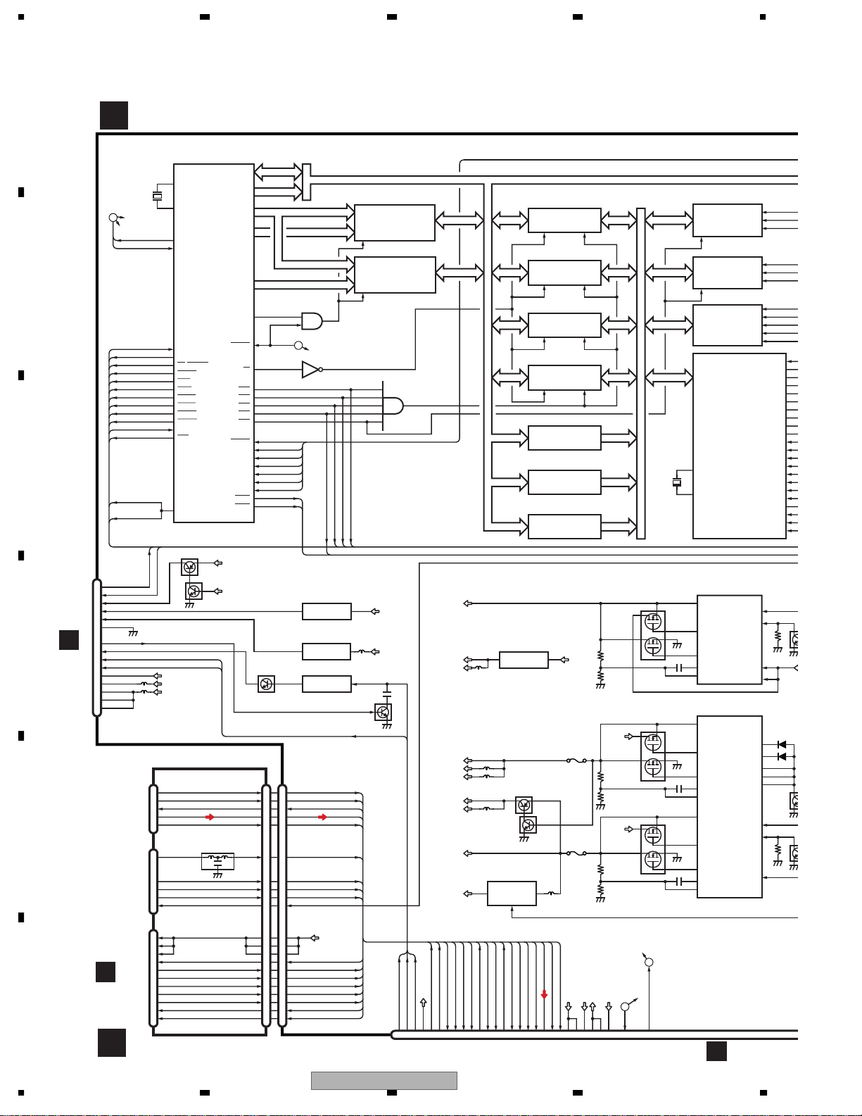
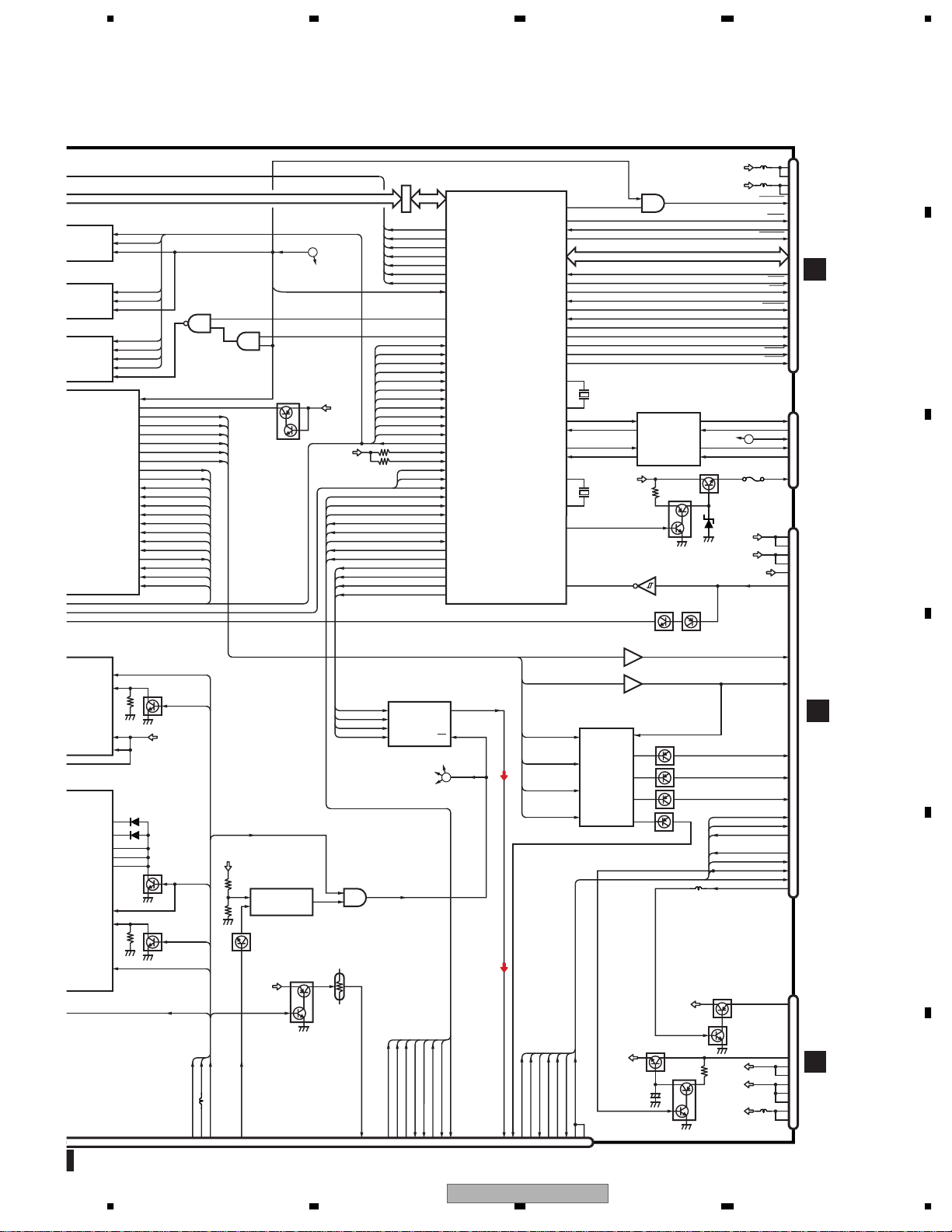
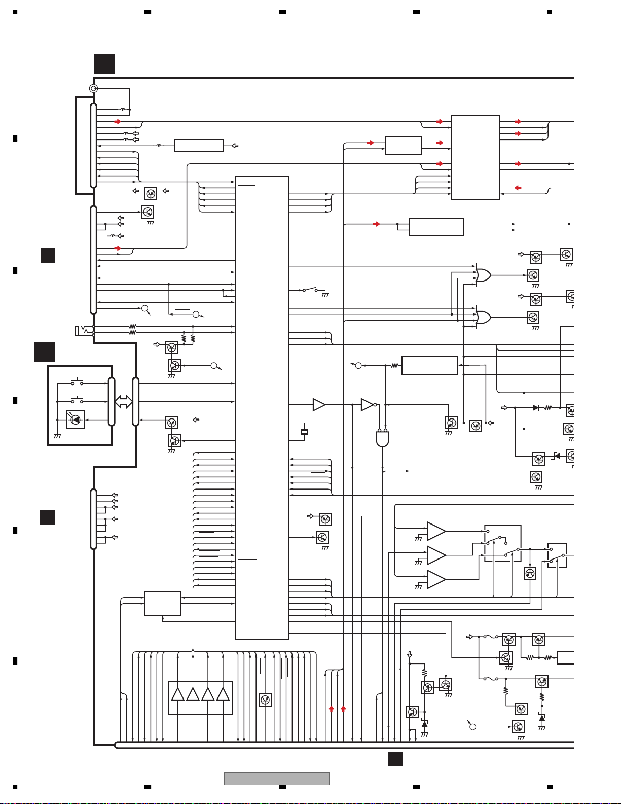
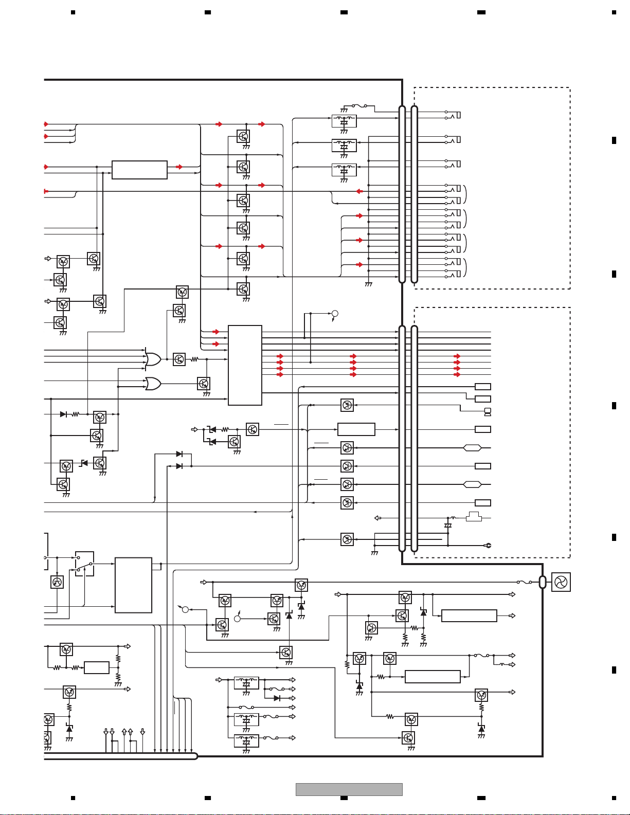
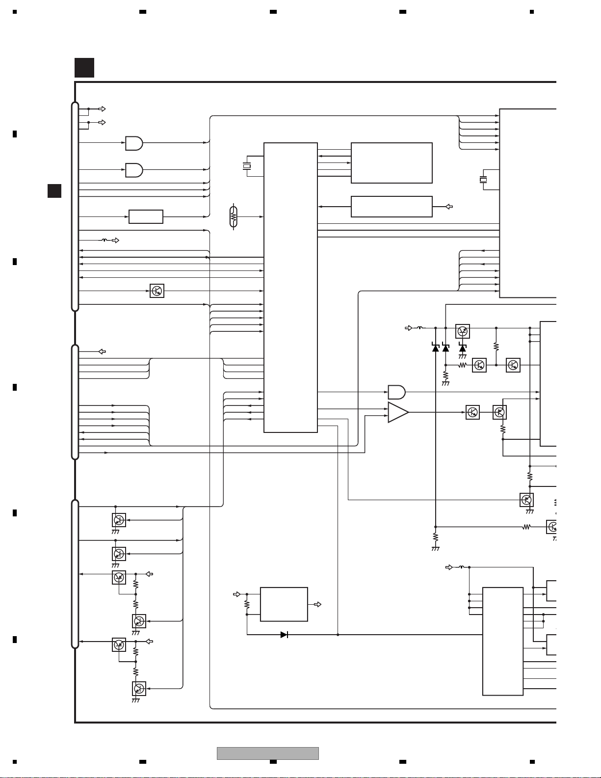
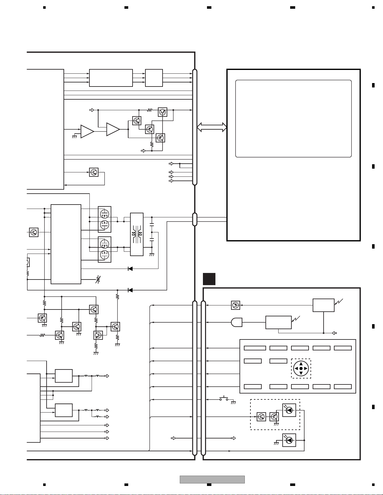
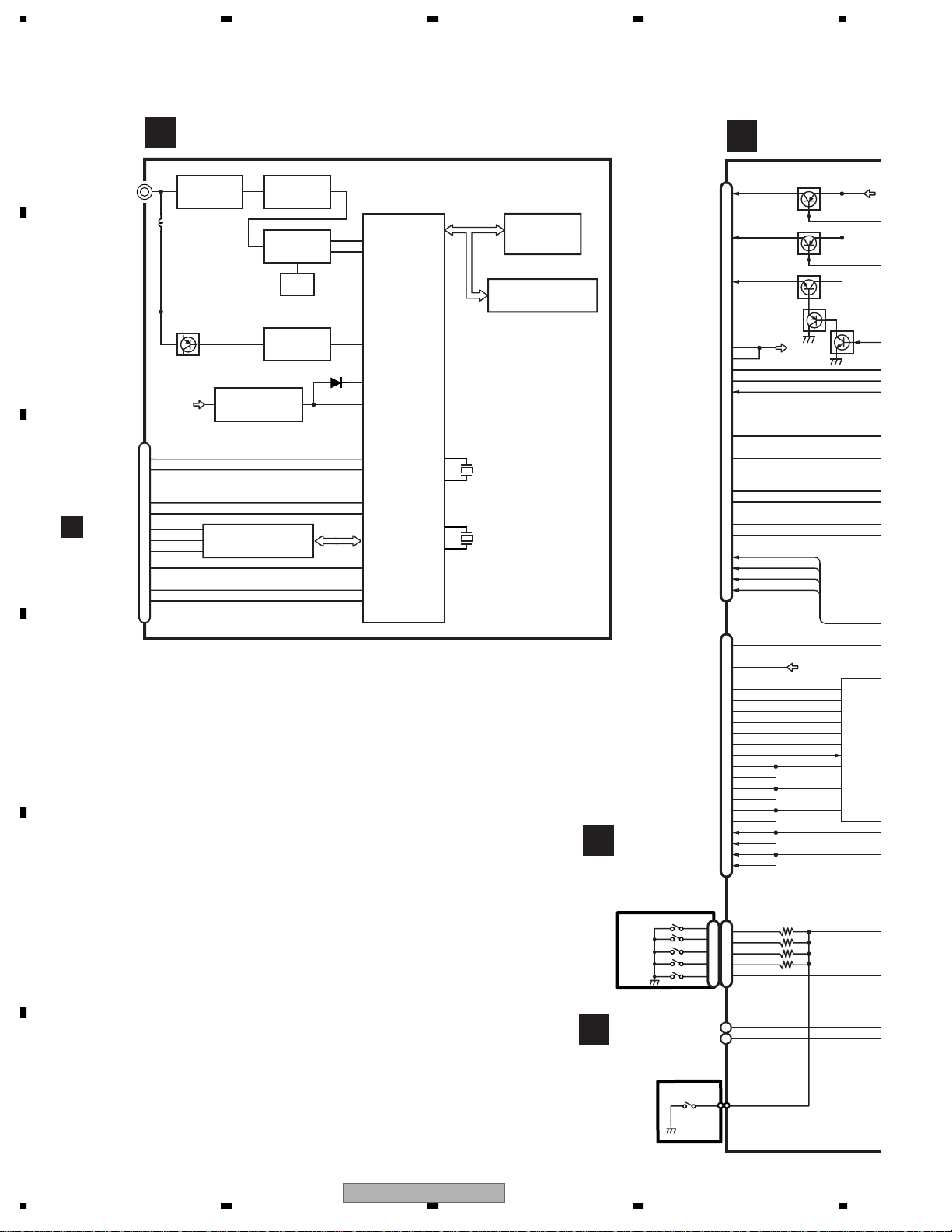
3. BLOCK DIAGRAM AND SCHEMATIC DIAGRAM
3.1 BLOCK DIAGRAM
A
A
CC UNIT
CPU
IC2
UPD705103GM-180S1
56
30.000MHz
A
X1
HYOKA
IRQPWR
X1
57
X2
78
PORTB0/TI
84
PORTB6/INTP02
B
GDC_DMARQ
GDC_DMAACK
XTC
XBCYST
XMRD
XMWR
XLLBEN
XLUBEN
XULBEN
XUUBEN
GDC_INT
XCS3
C
CPU_CLKGDC
CPU_CLKASIC
CN551
GPSTOC
19
CTOGPS
20
VSNS
10
GYROIN
11
GSNSIN
12
FLASHWE
14
PSWOUT
15
D
B
CN461
16
21
22
26
28
27
29
30
SPEED
REVSNS
RQ
BUP3
VCC3
VCC3
ANTVCC
IP-BUS
INPUT
E
AV-BUS
INPUT
L
CN2
F
K
20
1234
86
PORTA5/DMARQ3
90
PORTA7/DMAAK3
94
TC/STOPAK
107
BCYST
115
MRD
114
MWR
113
LLBEN
112
LUBEN
111
ULBEN
110
UUBEN
83
PORTB4/INTP01
99
CS3
PORTB7/INTP03
PORTB2/INTP00
PORTB3/INTP13
PORTA0/DMARQ0
PORTA2/DMARQ1
PORTA4/DMARQ2
46
CLKOUT
Q552
GPSTOC0
CTOGPS0
BUP3S
AD5V
CCD3
CN2802 CN702
BUS+
1
BUS−
5
ASENB
8
BUSL
7
BUSR
9
CN2801
COMP VIDEO
2
IP-SEL1
4
IP-SEL2
5
AV ON
12
10
CN2806
FLPBUP
15
14
13
FLPPW
8
OPENSW
7
HOMESW
6
CFSW
5
PULSE1
4
PULSE0
3
MOT1
2
MOT0
1
Q551
REVERSE
FLPBUP
AD5V
RQ
CONNECTOR UNIT
D0-31
1-23
A
XWE,XCAS,XRAS,XCS0,SDCKOUT
TC7SZ08FU
13
CKE
RST3
63
R/W
CS2
CS4
CS5
CS6
CS7
IORD
105
100
XCS2
982XCS4
974XCS5
9613XCS6
955XCS7
106
85
82
77
89
88
87
108
109
RST3
R/W
XREADY
INT0
INT2
INT3
DREQ0
DREQ1
DREQ2
XIORD
XIOWR
RESET
READY
IOWR
PULSE WA VEFORM CONV.
Q553
CN2804
BUS+
30
1
BUS−
29
BUSL
BUSR
VIDEO
AVON
CFSW
MOT1
MOT0
2
27
4
26
5
24
7
22
9
20
11
19
12
18
13
17
14
15
16
14
17
13
18
8
23
7
24
6
25
5
26
4
27
3
28
2
29
1
30
ASENB
IPSEL1
IPSEL2
REMOUTREMOUT
FLPBUP
FLPPW
OPENSW
HOMESW
PULSE1
PULSE0
SDRAM
IC1
K4S561632E-TL75
LLDQM,LUDQM
ULDQM,UUDQM
IC4
1
4
2
B
IC102
TC7SH04FUS1
24
XCS6
GYRO
GY551
CSX1054
41
VOUT VCC
G SENSOR
GY554
CSX1089
3
OUT VIN
1 5 SPEED
IC551
NJM2904M
BUS+
BUS−
ASENB
BUSL
BUSR
AVV
IPSEL1
IPSEL2
AVON
REMOUT
FLPBUP
FLPPW
OPENSW
OPENSW
CLOSESW
CLOSESW
CFSW
PULSE1
PULSE0
MOT1
MOT0
37
HY57V561620CLT-H
37
XCS5
XCS4
XCS2
1
Q554
REVERSE, RQ
BUSP
BUSM
ASENB0
BUSL
BUSR
AVV
IPSEL1
IPSEL2
AVON
MOTPW
CFSW
PULSE1
PULSE0
MOT1
MOT0
(256MBit)
SDRAM
(256MBit)
IC101
1
TC74LCX08FTS1
AD5V
AD5V
CN605
AVIC-D1/UC
IC3
11
RQ
REVERSE
REVERSE
SPEED SPEED
RQ
124
A2-16,D0-15
A2-16,D16-31
DVD8
BUP3C VDD5
BUP3S
CCD5C
CCV5
CCD5
CCD3C
CCD3
SD3VC
CCD25C
MOT0
MOT1
PULSE0
PULSE1
AD5V
MO0
MO1
PULSE0
PULSE1
3
789
10
S-818A33AUC-BGN
2.5V REG.
BA25BC0WFP
4
OUT
BUSP
BUSM
MOTPW
OPENSW
CLOSESW
BUS+
BUS−
MOTPW
OPENSW
CLOSESW
11
12131425171815
D0-7
D8-15
D16-23
D24-31
A1-8
A9-16
A17-23
3.3V REG.
IC802
VOUT VIN
3V REG.
Q801
IC801
VCC
CTL
1
AVON
CFSW
IPSEL1
ASENB0
ASENB0
IPSEL1
AVONIN
CFSW
16
BUS BUFFER
IC103
TC74LCX245FTS1
119
BUS BUFFER
IC104
TC74LCX245FTS1
119
BUS BUFFER
IC105
TC74LCX245FTS1
119
BUS BUFFER
IC106
TC74LCX245FTS1
119
BUS BUFFER
IC107
TC74LCX541FTS1
BUS BUFFER
IC108
TC74LCX541FTS1
BUS BUFFER
IC109
TC74LCX541FTS1
51
FU803
Q802
FU802
2
AVV
BUSL
BUSR
IPSEL2
CCD5
BUSL
BUSR
AVV
IPSEL2
19202242284041
CCD3
VDD5
VDD
697072
BUPV
BUPV
BD0-7
BD8-15
BD16-23
BD24-31
BA1-8
BA9-16
BA17-23
8.0V
5V
3.3V
SWAC56
B
RST3
54
BA2-23,BD0-15
BA2-23,BD16-31
BA1-17,BD0-15
BA2-23,BD0-31
X202
14.31818MHz
Q811
Q808
Q807
A
IRQPW IRQPWR
51
FLASH ROM
IC110
PEH007A
26
FLASH ROM
IC111
PEH008A
26
SRAM
IC113
M5M5V216ATP-
70HI
SCARLET
IC201
MB86291APFVS-
G-DL
124
CLK
128
OSCOUT
SWITCHING REG.
IC803
TPS5103IDB
18
LL
19
OUT_U
17
OUT_D
3
FB
2
INV
SWITCHING REG.
IC804
TPS5102IDBT
18
LL2
17
OUT2_U
19
OUT2_D
14
FB2
15
INV2
28
LL1
29
OUT1_U
27
OUT1_D
2
FB1
1
INV1
G
STBY
RT
VCC
VCC-SENSE
LH1
LH2
PWM_SKIP
VREF5
COMP
STBY2
RT
STBY1
CN1701
28
12
11
28 XMRD
12
17
41 XMRD
40
39 XLLBE
6
XRST
AOUTR
AOUTG
AOUTB
DCLKO
CSYNC
XRDY
XWE0
XWE1
XWE2
XWE3
DREQ
DRACK
DTACK
BCLKI
10
5
13
14
30
16
4
22
12
10
6
9
XINT
XBS
XCS
XRD
GV
A24
XMWR11
XMRD
XMWR
XMWR
XLUBE
SRAMC
S
44
129
152
147
143
202
204
207
99
97
115
114
116
179
117
118
119
120
98
107
108
113
Page 21
5678
A
H ROM
110
H007A
H ROM
111
H008A
RAM
113
V216ATP-
0HI
ARLET
C201
91APFVS-
G-DL
HING REG.
C803
5103IDB
STBY
VCC
VCC-SENSE
HING REG.
C804
102IDBT
LH1
LH2
PWM_SKIP
VREF5
COMP
STBY2
STBY1
CN1701
RT
RT
28
12
11
28 XMRD
12
17
41 XMRD
40
39 XLLBEN
6
XRST
AOUTR
AOUTG
AOUTB
DCLKO
CSYNC
XINT
XRDY
XBS
XCS
XRD
A24
XWE0
XWE1
XWE2
XWE3
DREQ
DRACK
DTACK
BCLKI
10
5
13
14
30
16
4
22
12
10
6
9
XMWR11
XMRD
XMWR
XMWR
XLUBEN
SRAMCS
44
129
S
152
147
143
202 FSC
204
207
GV
99 GDC_INT
GDC_WT
97
115
XBCYST
114
116
179
117
XLUBEN
118
XULBEN
119
XUUBEN
120
GDC_DMARQ
98
GDC_DMAACK
107
108
CPU_CLKGDC
113
Q804
BUPD1
Q805
Q803
DRAMPW
1 XCS_SRAM
4
2
AOUTRED
AOUTBLUE
OVER
XTC
CCON1
DRAMPW
DRAMPW
CCON
49
50
CCON1
CCD3C
CCON1
FCONT
FCONT
58
4
SYSRST
IC112
TC7SH00FUS1
AOUTGREEN
OUTCSYNC
XCS4
XMRD
XMWR
XLLBEN
CCON1
FCONT
CCON1
FCONT
CCON1
2
1
RESET GEN.
IC301
M51957BFP
2
IN1
5
Cd
Q301
VDD5
52
RST3
B
SRAM_CSE
IC114
TC7SH08FUS1
Q201
6
RSTOUT
Q601
CCD3C
CCD3C
KMODE
ILM
PBSNS
CPUWDT
XCCSTBY
SYSTOC
CTOSYS
ONSEIMUTE
DAC_MCLK
DAC_BCLK
DAC_LRCK
DAC_DATA
DAC_MCLK
DAC_BCLK
DAC_DATA
DAC_LRCK
IC302
TC7SH08FUS1
1
4
2
TH601
NTEMPIN
60
XREADY
INT0
INT2
INT3
DREQ0
DREQ1
DREQ2
XMRD
XLLBEN
GPSTOC0 30
DSP_HRDY
DSP_XHINT
XCS6
XIOWR
XIORD
DAC
IC304
AK4351VT
6
MCLK
3
BICK
4
SDATA
2
LRCK
RST3
ILM
PBSNS
KMODE
CPUWDT
KMODE
ISEN
PKBSNS
CPUWDT
434746
535557
94
176
175
174
172
173
240
108
11
44
170XCS2
171XCS3
238XCS5
169XBCYST
33CPU_CLKASIC
101GDC_WT
88
163XMWR
164
231XLUBEN
29CTOGPS0
75
76
97
90
165
85
48
126
127
49
110
27
129
135
134
56
55
AOUTL
PD
SYSTOC
CTOSYS
XCCSTBY
XCCSTBY
STOC
CTOS
56
ASIC
IC5
PD6336C
XREADY
INT0
INT2
INT3
DREQ0
DREQ1
DREQ2
XRESET
XCS_SRAM
PIO4
XCS2
XCS3
XCS5
XBCYST
CPU_CLK
GDC_WT
XMRD
XMWR
XLLBEN
XLUBEN
UART2_RX
UART2_TX
DSP_HRDY
DSP_XHINT
XCS6
XIOWR
XIORD
PIO28
PIO12
PIO11
PIO13
PIO14
UART3_RX
UART3_TX
PIO17
DAC_MCLK
DAC_BCLK
DAC_LRCK
DAC_DATA
5
RST3
B
ONSEIMUTE
ONSEIMUTE
59
DACOUTL11
RST3
GUIDE
NAVIV
343137
PIO29
PIO3
PIO18
ATA_XRESET
0-15
ATA_DD
ATA_DMARQ
ATA_XDIOW
ATA_XDIOR
ATA_IORDY
ATA_XDMACK
ATA_INT
ATA_DA1
ATA_DA0
ATA_DA2
ATA_XCS0
ATA_XCS1
EXTAL0
XTAL0
UART7_TX
UART7_RX
UART5_TX
UART5_RX
EXTAL1
XTAL1
PIO9
IR_RX
OVER
OUTSYNC
AOUTBLUE
AOUTGREEN
AOUTRED
FSC
STOM
MTOS
MONVBS
SWACPW
FMONV
STOM
MTOS
SWACPW
62646366677677
RST3
IC309
TC7SH08FUS1
2
4
12 XRSTMS3
51 DISC
182
109
246
181
180
179
178
177
191
257
192
X2
18
33.000MHz
16
21
CTOEX0
104
EXTOC0
CTOB0
25
BTOC0
24
60
BUPD1
X3
33.8688MHz
58
ANTON0
125
14
REMOUT
1,2
1,2
NTSC ENCORDING
IC752
BH7236AF
4
SYNCIN
BIN
BOUT
3
GIN
GOUT
2
RIN
ROUT
6
SCIN VOUT
PWRVI
PWRVI
ILMB
HDRST
MEMLED
SWACPW
MEMOLED
HDRST
KEYILM
DVDEJECT42
ATA_XRESET114
ATA_DD0-15
ATA_DMARQ
ATA_XDIOW
ATA_XDIOR
ATA_IORDY
ATA_XDMACK
ATA_INT
ATA_DA1
ATA_DA0
ATA_DA2
ATA_XCS0
ATA_XCS1
RS232C DRIVER
IC651
UPD4721GSS1
7
DIN1
9
ROUT1
8
DIN2
10
ROUT2
IC602
TC7SH14FUS1
42
Q604 Q603
IC751
TC7SH08FUS1
4
IC753
TC7SH08FUS1
4
10
21
22
23
20
PWRFL
MFLPW0
Q809
+
DOUT1
DOUT2
Q651
Q753
Q752
Q751
Q754
Q806
RIN1
RIN2
14
12
13
11
PWRFL
Q813
FLPBUP
DVD8
CCD5
Q652
PWRFL
PWRVI
MONVBS
ILMB
HDRST
MTOS
STOM
SWACPW
MEMLED
Q814
BUPD1
BUPV
FU651
SWAC56
A
VDD8
VDD5
XRESET
EJSW
HRESET
DMARQ
DIOW
DIOR
IORDY
DMACK
INTRQ
DA1
DA0
DA2
CS1FX
CS3FX
CN2
CN651
CTOEX
EXTOC
HYOKA
CTOTA
TATOC
CN701
MOREMREM_IN0
CSYNC
ANB
ANG
ANR
MONVBS
ILMB
HDRST
MTOS
STOM
SWACPW
MEMLED
MFLPWMFLPW0
CN801
PWRFL
PWRVI
VTA
YS
38
37
36
35
34
33
32
28
27
|
12
11
C
10
9
8
7
6
5
4
3
2
1
4
5
6
7
XM TUNER
8
9
1
2
7
8
23
26
13
15
17
18
19
21
22
25
28
29
32
33
31
1
3
5
G
6
9
10
11
18
20
TO
H
CN601
CN5002
CN1802
B
C
D
E
F
56
AVIC-D1/UC
7
8
21
Page 22
2
O
E
D
0
1234
G
A
SYSTEM UNIT
CN4300
AM_ANT
1
FM_ANT
3
Lch
Rch
VCC
ROM_VDD
VDD_3.3
SL
CE2
CE1
CK
DI
DO
CN1301
CD3VON
VD2
VD
VDD
LOUT
ROUT
BRST
BRXEN
BSRQ
CSENS
RESET
BDATA
BSCK
VDCONT
WCONT
WREMIN
CN1802
BUPV
TUNPDO
5
4
2
TUNL
TUNR
TUNSL
TUNCE2
TUNCE1
TUNCK
TUNPDI
CDL
CDR
PWRFL
PWRVI
FLPBUP
BUPD
BACKUP2
BUS−
BUS+
BUS−
VD56
VD83
VDD5
MEMOLED
BUS+
VDORA85
VDD5
VD2
A
VDD2
Q1920
Q1924
VD83VD56
IC4301
NJM2391DL1-33
RESET
Q1501
CN1651
DVEJKY
5
CDEJKY
4
FLAPILM
PNLILM
2
IP-BUS DRIVER
HA12240FP
5
BUS−
6
BUS+
TC74VHCT08AFTS1
MTOS
STOM
NTEMPI
Q1940
IC1601
STBN
8
3V→5V
IC1501
STOC
FCONT
DIN1
DOUT
Q1941
CTOS5
11
12,13
3.3V REG.
B
(1/2)
CCON
Q1501
(2/2)
MEMOLED
MTOS
STOM
NTEMPI
FCONT
STOC
CTOS5
XCCSTBY5
RST3U
CPUWDT
SYSRST
DRAMPW
VSELIN2
VSELIN1
AVONIN
CFSW
MOTPW
CLOSESW
OPENSW
PULSE1
PULSE0
MOT1
MOT0
1
2
XCCSTBY5
6
4,5
TUNSL
TUNCE2
TUNCE1
TUNCK
TUNPDO
TUNPDI
BUP
RST3U
8
9,10
C
CPUWDT
3
1,2
13
VDORA85
SYSTEM MICRO
77
TUNSL
96
TUNCE2
95
TUNCE1
99
TUNCK
98
TUNPDO
97
TUNPDI
13
BRST
30
BRXEN
14
BSRQ
3
CSENSOUT
34
RESET
15
BSI
16
BSO
17
BSCK
80
WCONT
79
WREMIN
93
DVDEJECT
94
CDEJECT
62
FLAPILM
63
MEMOLED
6
MTOS
7
STOM
78
TEMP
2
FCONT
1
STOC
100
CTOS
82
XCCSTBY
81
RST3
83
CPUWDT
57
SYSRST
54
DRAMPW
19
VSELIN2
18
VSELIN1
20
AVONIN
50
EJECTSW
47
MOTPW
49
HOMESW
48
OPENSW
44
PULSE1
43
PULSE0
46
MOT1
45
MOT0
27
TX
26
RX
28
IPPW
SYSRST
DRAMPW
IC1502
PE5478A
MUTEAMP
AVONIN
VSELIN2
VSELIN1
22
VCK
23
VDT
VST
MUTEVOL
NOSELL
EQSW
NOSELR
MUTENS
MUTEALL
AMPSTBY
IRQPW
REVSENS
PBSENS
ANTPW
BSENS
ASENS
ILMSEN
TELIN
ASENB0
VFSEL0
VFSEL1
VRSEL
REARON
CCON
FANUP
SWACPW
SYSPW
ILMPW
CFSW
Q1502
X1
X2
MOTPW
CLOSESW
VDT
24
VST
25
MUTEVOL
52
S1501
4
53
51
68
MUTEAMP
67
MUTEALL
65
AMPSTB
5V→3V
IC1503
TC7SH08FUS1
56 1,2 4 2 4
39
X1501
12.58MHz
38
86
REVSNS
85
PKBSNS
60
ANTPW
90
BSENS
91
ASENS
92
ISENS
84
TELIN
Q1601
BUP
29
Q1602
69
VFSEL0
70
VFSEL1
72
VRSEL
73
REARON
55
CCON
66
FANUP
11
SWACPW
12
61
MOT1
MOT0
PULSE1
PULSE0
OPENSW
BUSL
BUSR
DACOUTL1
ONSEIMUTE1
BUSL
BUSR
ONSEIMUTE1
B
IC1505
TC7S04FU
IRQPW3
RESET
12
HDRST
IC4401
TA2050FS1
13
IN1A
12
IN2A
1
RESET
TC7SH00FUS1
4
RQ
HDRST
RQ
1
OUT1
8
OUT2
VCK
VDT
VST
MUTEVOLVCK
NJM2068V
3DACOUTL1
A+INPUT
5
B+INPUT
NOSELL
NOSELR
MUTENS
ONSEIMUTE1
RESET
IC1506
S-80840CNMC-B8Z
IC1507
VIDEO ISOLATOR
3
VCRINV
2
3
AVV
2
3
BACKV
2
BUP
ILMPW
Q1942
23
24
4
13
17
5
6
8
9
FM/AM TUNER UNIT
10
14
B
F
CN901
WIRED
C
REMOTE
J
PANEL PCB
CN1450
S5902
S5901
D5901-D5906
1
2
3
4
5
10
12
6
7
8
14
15
17
18
19
CN5901
DVEJKY
CDEJKY
PNLILM
D
20
18
16
15
A
CN801
12
11
10
3
1
E
F
MEMOLED
MTOS
STOM
NTEMPIN
FCONT
22
BUS−
CN1701
BUS+
STOC
151866671921232524
CTOS
XCCSTBY
26
1234
RST3
27
SYSRST
CPUWDT
282932
DRAMPW
IPSEL2
IPSEL1
CFSW
MOTPW
CLOSESW
AVONIN
6364686970717273744456
61
62
AVIC-D1/UC
OPENSW
PULSE1
PULSE0
MO1
MO0
ONSEIMUTE
GUIDE
BUSR
22
BUSL
59
IRQPW
30
ASENB0
657814
HDRST
RQ
AVV
FMONV
53
A
NAVIV
50
47
CN605
KEYILM
4
5
TUNL
TUNR4038
CDL
CDR
LPF
IC4500
A_OUTPUT
B_OUTPUT
+
−
IC1002
NJM2137V
+
−
IC1001
NJM2137V
+
−
IC1003
NJM2137V
Q1943
(1/2)
AUDIO SELECT
IC4001
PML009A
IN1L
Rearout_L
IN1_R
Rearout_R
Preout_L
IN2L
IN2_R
IN3L
IN3_R
CLK
DAT A
STB
MUTE
2
1
7
D4500-D4503
RESETM
Preout_R
Frontout_L
Frontout_R
IN4+_L
IN4+_R
Q1503
(2/2)
41
37
42
36
17
18
19
20
Q1503
(1/2)
FRONT VIDEO SELECTOR
11
3
1
1
BUP
Q1943
(2/2)
5
FU1900
Q1904
FU1920
VDCONT
A
11
23
12
22
10
24
43
35
AV85
AV85
MUTEAMP
MUTEALL
AMPSTB
MBUP
VDD5
IC1201
NJM2235V
2
4
VFSEL0
VDORA85
Q1903
Q1923
(2/2)
RL1
RR1
SWL1
SWR1
VCRINL
VCRINR
L/R SW(MUTE)
Q4503
(1/2)
Q4503
(2/2)
Q4500
(1/2)
Q4500
(2/2)
Q4202
(1/2)
REAR VIDEO SEL
Q1201
VFSEL1
FMONV
NAVIV
Q1902
Q1922
VD
Q1923
(1/2)
Q4501
Q4502
Q4211
(2/2)
Q4202
(2/2)
IC1202
NJM2235V
17
3
2
VRSEL
REAR
IC19
M5237
1SYSPWR
IN
Q42
(1/
7
A
Page 23
5678
A
RL1
RR1
SWL1
SWR1
VCRINL
VCRINR
L/R SW(MUTE)
4503
503
/2)
500
/2)
L
1/2)
4500
1/2)
P
Q4202
(1/2)
Q4211
Q4202
(2/2)
(2/2)
Q4501
Q4502
Q4211
(1/2)
ECTOR
REAR VIDEO SELECTOR
IC1202
NJM2235V
17
7 4
3
2
1201
NV
IV
RA85
VD
1923
1/2)
Q1902
Q1922
VRSEL
REARON
IC1900
M5237ML
IN
ADJ
AUDIO MIX AMP
IC4100
NJM2058V
9
C_INPUT
6
B_INPUT
D4200,D4201
MUTEAMP
MUTEALL
RESETM
OFMT
RESETM
OFMT
Q4201
IC1204
NJM2561F1
Vin
1
POWER_SAVE
VDORA85
31
VD83
CCD5
CCD3
VDD5
SWAC56
VDD
9
394012
113441
D_OUTPUT
A_OUTPUT
D4204
Vout
Vsag
AD5V
778017
REVSNS
2
3
CCON
SWACPW
SWACPW
CCON
31
14
1
Q4210
(1/2)
Q4210
(2/2)
Q4209
RSMT
PKBSNS
REVERSE
PKBSNS
BUP
ISENS
ISEN
FL1
FR1
BUP
C
CCON
FANUP
SWACPW
KMODE
SPEED SPEED
KMODE
383579
Q4212
CCON
RL1
RR1
SWL1
SWR1
FL1
FR1
MUTERCA
FL1
FR1
RL1
RR1
Q1881
MBUP
POWER AMP
IC4200
PAL007B
12
FLIN
11
FRIN
14
RLIN
15
RRIN
22
MUTE
B.REMOTE
4
STBY
Q1882
D
FU1820
REARV
RL
Q4205
Q4208
Q4207
Q4206
Q4203
Q4204
RR+
FR+
RR−
FR−
RL+
FL+
RL−
FL−
B SENS
Q1860
(1/2)
Q1860
(2/2)
FANCNT
Q1833
(2/2)
+
+
+
17
9
19
7
21
5
23
3
25
BACKV, VCRINV
FU1821
FU1830
BACKV
RR
VCRINV
SWL GNDVCRL
SWR SWL
FL GNDA
FR FR
BSENS
REARV
KMODE
Q1884
Q1833
(1/2)
Q1885
BUP
FU1823
BUPD
BACKUP2
FLPBUP
PWRFL
PWRVI
VCRINL
VCRINR
FANCNT
D
PKBSNS
Q1802
ANTENNA ON
ANTPW
ASENS
Q1861
Q1810
ISENS
TELIN
K MODE
BACKUP2 AV85
FU1401
+
+
+
SWL
SWR
RL
RR
FL
FR
SPEED PULSESPEED
SYSTEM REMOTEBREM
PARKING SENS
PARKING BRAKE
IC1801
TPD1018F
A SENS
REVERSE SENS
REVERSE SIGNAL
ILM SENS
Q1820
TEL MUTE
Q1821
MBUP
Q1960
Q1842 Q1841
CN1401
BACKVG
GNDVCRR
CN1801
16
AV85
GNDVR
REARV
BACKV
GNDVV
VCRV
VCRL
VCRR
GNDA
GNDA
SWR
GNDA
GNDA
GNDA
RR+
FR+
RR−
FR−
A.ANT
ACC
MUTE
B.UP
VGND
KMODE
GND
Q1901
(1/2)
Q1901
(2/2)
RL
RR
FL
RL+
FL+
RL−
FL−
ILL
CORD ASSY(AV)
GNDVR
1
1
REARV
2
2
BACKVG
5
5
BACKV
6
6
GNDVV
7
7
VCRV
8
8
GNDVCRL
9
9
VCRL
10
10
GNDVCRR
11
11
VCRR
12
12
GNDA
13
13
SWL
14
14
GNDA
15
15
SWR
16
16
GNDA
17
17
RL
18
18
GNDA
19
19
RR
20
20
GNDA
21
21
FL
22
22
GNDA
23
23
FR
24
24
REAR MONITOR OUTPUT
BACK CAMERA INPUT
VIDEO INPUT
AUDIO INPUT
SUB WOOFER and NON FADER OUTPUT
REAR
FRONT
CORD ASSY(POWER SUPPLY)
RR+
1
1
FR+
2
2
RR−
3
3
FR−
4
4
RL+
5
5
FL+
6
6
RL−
7
7
FL−
8
8
SPEED PULSE
9
9
SYSTEM REMOTE
10
10
PARKING BRAKE
11
11
A.ANT
12
12
ACC
13
13
REVERSE SIGNAL
14
14
ILL
15
15
MUTE
16
16
B.UP
17
17
VGND
18
18
KMODE
19
19
GND
20
20
Q1900
VDD5V REG.
IC1840
S-812C50AUA-C3E
Q1850
(1/2)
Q1850
(2/2)
+
AD5V REG.
IC1902
S-812C50AUA-C3E
32
Q1851
RR+
FR+
RR−
FR−
RL+
FL+
RL−
FL−
CAR SPEED SIGNAL INPUT
SYSTEM REMOTE CONTROL
PARKING BRAKE
AUTO-ANTENNA REMOTE CONTROL
1KΩ
ACC
REVERSE-GEAR SIGNAL INPUT
1KΩ
ILL
CELLULAR MUTE
10A
BACK UP
GND
FU1840
SWAC56
B
C
D
FAN MOTOR
CN1803
FU1880
2
32
AD5V
VDD5
VDD2
SWAC56
E
F
56
AVIC-D1/UC
7
8
23
Page 24
O
T
X
H
C
V
O
N
T
T
0
A
C
Z
V
5
5
1234
A
B
CN701
C
D
A
H
MONITOR PCB
CN5002
PWRFL
1
2
7
8
13
15
17
18
19
21
22
23
25
26
28
29
31
32
33
BUP (VFL)
PWRVI
BUP (V14)
YS YS
NVSYNC NVSYNC
NVBLUE
NVGREN ANG
NVRED
CSYNCO
ILMB
ACC5V
HDRST
REMIN REMIN
MTOSYS
SYSTOM
MFLPW 10
SWACPW
MEMLED
TC7SH08FUS1
TC7SH00FUS1
1,2
FILTER
Q5101-Q5103
VSW5V
IC5061
41,2
IC5026
4
Q5603
ANB
ANR
CSYNCO
ILMB
HDRST
MEMLED
X5601
TEMP.Sens
TH5601
KDT0
KDT1
KDT2
KDT3
LSEN
CN5009
VCC
OSDCS
OSDCK
OSDDT
EPRTES
OSDR
OSDG
OSDB
BLK
OSDV
SCKE
OSDH
DIMOFF
V332
OSDCS
OSDCK
OSDDT
EPRTES
OSDR
OSDG
OSDB
BLK
OSDV
SCKE
OSDH
OSDCS
OSDCK
OSDDT
EPRTES
PNLADY
PNLADX
PNLVD
PNLXV
PNLYV
20
19
18
17
3
14
13
12
11
10
9
8
2
MONITOR CPU
IC5601
PE5479A
70
X1
69
X2
80
TEMPSEN
61
REMIN
9
TXD
8
RXD
MFLPW
62
VDDSENS
76
KEY0
77
KEY1
78
KEY2
79
KEY3
2
LSEN
14
OSDCS
18
OSDCK
17
OSDDT
21
EPRTEST
3
PNLADY
1
PNLADX
31
PNLVD
24
PNLXV
25
PNLYV
EPRPROT
EPRDI
EPRDO
EPRSK
EPRCS
RESET
SDA
SCL
PIPRES
INVPUL
DIMMER
INVBST_DA
MVIPW
50 8
49 6
48 5
47 4
46 3
60 1
44
5
6
13
EEP-ROM
PRO
DO
DI
SK
CS
IC5651
S-29221BROI-J8T1
POWER ON RESET
IC5602
S-80835CNNB-B8U
BUP (VFL)
IC5333
TC7SH08FUS1
6
2,5
DIMMER BLOCK
IC5901
NJM2903V
VIDEO PROCESS BL
IC5001
TC90A64AF-P
YS
NVSYNC
ANB
ANG
ANR
CSYNCO
2
VSW5V
SCKE
OSDH
OSDV
BLK
OSDB
OSDG
OSDR
Q5351
41,2
7
93
18
54
53
52
65
82
X5001
83
9927
9628
10429
101
9
100
92
91
90
89
INVERTER
Q5343 Q5342
Q5332
Q5331
FNAVI
HDIN
BIN
GIN
RIN
CVI1
XO
XI
IICDA
IICCK
RESET
SCKE
CLAMP0
NDSV
BLNK
OSDB
OSDG
OSDR
ROU
GOU
BOU
STH1
C
CP
POL
CP
STV1
CDA
CKI
I
O
5
VDD
14
DIM
15
LCT
3
ENA
18
CT
7
V250
9
FB
IC5851
BD6171KV
PVCC1
OUT2
PVCC2
DVCC
PVCC3
VCC
PVCC4
PVCC5
EN1
OUT1
OUT3
OUT4
OUT5
Q5373
VS2
VS1
Q5371
8V
4
7
3
Q
4
23
48
37
3.3
4
10
3
Q
13
22
47
38
CN5007
PNLADY PNLADY
4
Q5683
(1/2)
PNLADX
3
Q5683
(2/2)
PNLXV
E
2
Q5682
(1/2)
TOUCH PANEL
Q5682
(2/2)
PNLYV
1
Q5681
(1/2)
Q5681
(2/2)
PNLVD
PNLADX
PNLYV
VSW5V
PNLXV
VSW5V
PNLYV
V332
2.5V REG.
2
IC5841
R1130H251B
5
(BUP)V14
1
V25
D/D CONVERTER
11
6
41
42
32
F
24
1234
AVIC-D1/UC
Page 25
O PROCESS BLOCK
IC5001
TC90A64AF-P
FNAVI
HDIN
BIN
GIN
RIN
CVI1
XO
XI
IICDA
IICCK
RESET
SCKE
CLAMP0
NDSV
BLNK
OSDB
OSDG
OSDR
ROUT
GOUT
BOUT
STH1
CPH
POLC
CPV
STV1
CDAO
CKIN
CX
5678
RGB AMP
34
36
38
14 STH1
13 CX
8
28 6
4 CPV
2
72
74
IC5151 NJM2138V
V8
-
72
5
+
VCOM AMP
IC5181
NJM082BV
Q5002
Q5151
3,8
-
Q5153
+
-
Q5182
1
(1/2)
VM12
Q5183
(1/2)
Q5154
|
Q5156
Q5182
(2/2)
V332
V18
VM12
V5
Q5183
(2/2)
CN5801
CPH
VCOM
STV1
VDD3
VGH
VDD5
VGL
A
VR
28
VG
27
VB
26
24
22
20
17
B
7
5
L/R
23
12
15
13
2
LCD PANEL
TER
Q5342
Q5373
VERTER
851
71KV
OUT2
VS2
PVCC3
PVCC4
PVCC5
OUT1
VS1
OUT3
OUT4
OUT5
IC5331
OZ961ISN
520
VDDA NDRV_B
14
DIM
15 5
LCT
19
ENA
CT
V2500
FB
Q5371
8V REG.
4
3
Q5832
3.3V REG.
4
3
Q5831
PDRV_A
NDRV_D
PDRV_C
OVP
Q5372
RT
1,2,5,6
1,2,5,6
11
12
17
2
Q5380
VR5331
Q5375
(2/2)
Q5375
(1/2)
V8
V33
V332
V5
V18
VM12
3
18
7
9
7
4
23
48
37
10
13
22
47
38
Q5333
Q5334
4
3
2
T5331
6
7
LSEN
REMIN REMIN
KDT3
KDT2
KDT1
KDT0
HDRST
MEMLED
VSW5V
ILMB
CN5331
FLP
FLW
CN5008
LSEN
KDT3
KDT2
KDT1
KDT0
HDRST
MEMLED
REMPWR
ILMB
1
2
I
KEYBOARD PCB
CN5700
LSEN
2
2
REMIN 2
3
3
KDT3
4
4
KDT2
5
5
KDT1
6
6
KDT0
7
7
HDRST
8
8
MEMLED
10
10
REMPWR(5V)
11
11
ILMB(10V)
12
12
Q5703
4
IC5701
TC7SH08FUS1
S5700
RESET
REMOTE CONTROL SENSOR
1,2
S5715
DESTINATION
S5709
WIDE
S5701 S5702
SOURCE
REMPWR
SBX3050-01
Q5701
IC5700
1
S5716
ANGLE
S5710
MEMO
VOL−
Q5702
OPTICAL SENSOR
4
IC5702
TPS850
S5717
OPEN INFO
S5713
S5703
VOL+
D5712
S5719
TRAFIC
S5704
D5700-D5711
D5713-D5716
C
D
3
REMPWR
S5720
E
S5718
AV MAP
F
56
AVIC-D1/UC
7
8
25
Page 26
O
E
/
A
V
1234
A
B
GPS UNIT
CN504
1
GPS
ANTENNA
IC 401
UPC2749T
B
Q441
BUP3V
4
2
5
1
RESET
6
IC 504
MAX6364PUT29
F401
CTF1548
IC 402
UPB1027GS
19
X401
16.368MHz
IC 441
NJM2100V
1
4
FLASH ROM
22
143
IF
17
110
CRCK
IC 501
PD3390A
DRAGON
130
PIN0
131
140
120
CPU
PIN1
BOWWOWB
RESETB
7
IC 502
PD6519A
DRAM
IC 503
M5M5V216ATP-70HI
CN461
RQ
22
REVSNS
21
SPEED
16
PSWOUT
C
CN551
A
15
13
11
12
3
3
20
19
SL
GYROIN
GSNSIN
SD
CTOGPS
GPSTOC
1
2
IC 461
3
ADC12H034CIMSAS1
132
133
128
PIN2
PIN3
9
SPEED
17
ADIO2
28
PLIO2
PLIO2
8
RXD0
7
TXD0
XAUXIN
XAUXOUT
XRTCIN
XRTCOUT
129
102
103
X502
20.00MHz
X501
32.768kHz
D
D
COMPOUND
C
DVD CORE U
CN1101
65LD
26
78LD
24
VSHF
23
PICKUP UNIT(SERVICE) CARRIAGE MOTOR
VCC
19
MDC
9
VREF
22
TEMP
20
SW
18
A
17
B1
16
B2
15
−
RF
14
B3
13
+
RF
12
B4
11
C
10
65MD
7
78MD
5
+
F
4
−
F
3
−
T
2
+
T
1
Q1104
VCC5
Q1101
Q1102
Q1105
FOP
FOM
TOP
TOM
Q1103
CD
T
CN1201
SWITCH
20
+
HALL_BIAS
18
SPINDLE MOTOR
17
16
15
14
13
12
11
10
9
8
7
6
5
4
3
2
1
+
HALL_U
−
HALL_U
+
HALL_V
−
HALL_V
HALL_W
HALL_W
HALL_BIAS
COIL_U
COIL_U
COIL_W
COIL_W
COIL_V
COIL_V
CRGD1
CRGD2
CRGR1
CRGR2
+
−
−
VCC5
8
9
10
11
12
13
14
6
4
5
IC1202
BA6859
+
H1
−
H1
+
H2
−
H2
+
H3
−
H3
VH
A1
A3
A2
UNIT(A)
2
3
4
5
6
CN1202
12cm
5
8cm
4
disc ditect
3
8cm
2
Photo
1
E
12cm
8cm
Disc sens
Disc sens
8cm
S1201
S1202
S1203
S1204
S1205
LOADING
MOTOR
E
COMPOUND
UNIT(B)
F
26
1234
AVIC-D1/UC
CLAMP SW
S1206
Page 27
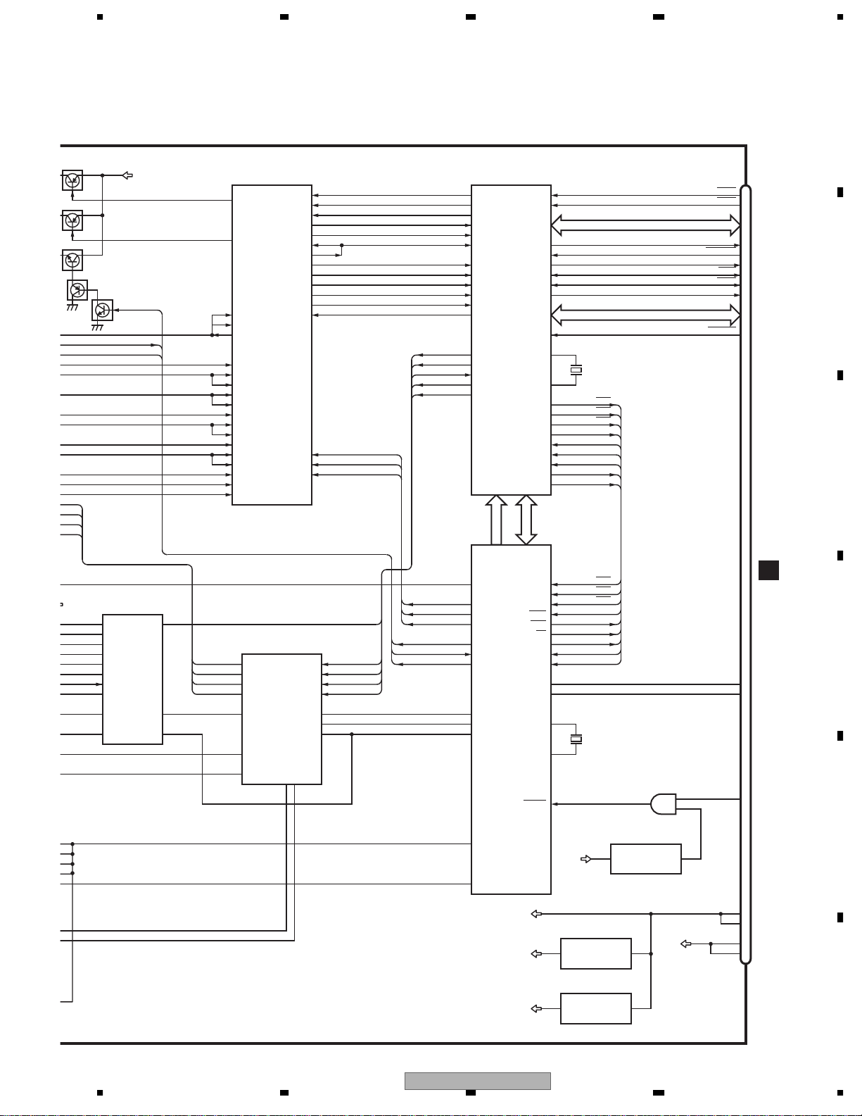
CORE UNIT
5678
A
Q1101
Q1102
Q1105
C5
FOP
FOM
TOP
TOM
VCC5
Q1103
CD/DVD
IC1202
BA6859AFP-Y
8
+
H1
9
−
H1
10
+
H2
11
−
H2
12
+
H3
13
−
H3
14
VH
6
A1
4
A3
5
A2
VCC5
TEMP
OEIC
IC1101
AN8703FH
FEP
2
LPCO1
4
LPCO2
53
VIN9
54
VIN10
56
VREF1
63
VIN12
57
VIN1
49
VIN5
58
VIN2
50
VIN6
48
RFINN
59
VIN3
51
VIN7
47
RFINP
60
VIN4
52
VIN8
62
VIN11
1
LPC1
3
LPC2
TBAL
FBAL
JLINE
TEOUT
ASOUT
FEN
FEOUT
DFLTON
DFLTOP
OFTR
BDO
RFENV
TESTSG
SEN
SCK
STDI
6
7
16
18
20
21
22
30
31
39
40
41
46
FD
TD
FG
MD
CRGDRV
12
13
14
LTFEP
SCKCOMN
SOCOMN
IC1301
MNZS26EDCUB
SODC
65
TBAL
66
FBAL
84
JLINE
118
AD1
119
AD2
117
AD0
110
NARF
111
ARF
51
OFTR
52
BDO
120
AD3
82
TESTSG
115
DAC1
114
DAC0
69
FG
68
SPDRV
67
TRSDRV
A0-17
IC401
PE5430A
CPU
79
P75
LTFEP
SCKCOMN
22 FG
FG
IC1201
BA5985FM
18
TOP
TOM
FOP
FOM
20 7 18
EC
PS
17
16
15
13
14
VO3(+)
VO3(−)
VO4(+)
VO4(−)
OUTPUT2
VO1(−)
VO1(+)
VOL+,910
26
OPIN4(−)
OPIN3(−)
OPIN2(+)
OPIN1(−)
FWD
REV
MUTE
FD
23
TD
5
MD
3
CRGDRV
28 9
21 1021
SOCOMN
CD/DVD
TEMP
OEIC
91
P05
96
SCK0
95
SO0
99
P15
74
ANI0
93
P07
TO2
TO3
P30
75
ANI1
76
ANI2
NCS3FX
NCS1FX
INTRQ
NDMACK
IORDY
NIORD
NIOWR
DMARQ
NRESET
OSCO1
OSCI1
NINT0
NINT1
NINT2
WAITODC
NWR
NRD
NRST
MONI0
MONI1
D0-7
INTP0
INTP1
INTP3
WAIT
WRL
P25
P83
P82
P96
P74
RESET
136
135
141
142
145
146
147
148
175
80
X1301
79
1
2
5
6
WAITODC
35
XWR
36
47
XODCRES
127
DVDLOCK
128
CDLOCK
87
88
90
39
WAITODC
40
XWR
43
RD
5
XODCRES
85
DVDLOCK
84
CDLOCK
46
78
36
X1
X2
X401
16.00MHz
35
31 4
VCC33
HDD0-15
INT0
INT1
INT2
XRD
INT0
INT1
INT2
XRD
IC402
S-80827CNNB
-B8M
DA0-2
IC404
TC7S08F
CN601
HCS1
45
HCS0
44
43
|
41
HINTRQ
40
HDMACK
39
IORDY
38
DIOR
37
DIOW
HDMARQ
HRESET
36
35
34
|
19
18
B
C
CN2
A
D
DISC
14
EJ
13
XRESET
1
2
12
E
12
VCC5
VCC33
VCC18
AVIC-D1/UC
56
3.3V REG
IC601
BA033FP
1.8V REG
IC602
BA18BC0FP
7
11
10
DVD8
VD8
13
13
9
8
F
8
27
Page 28
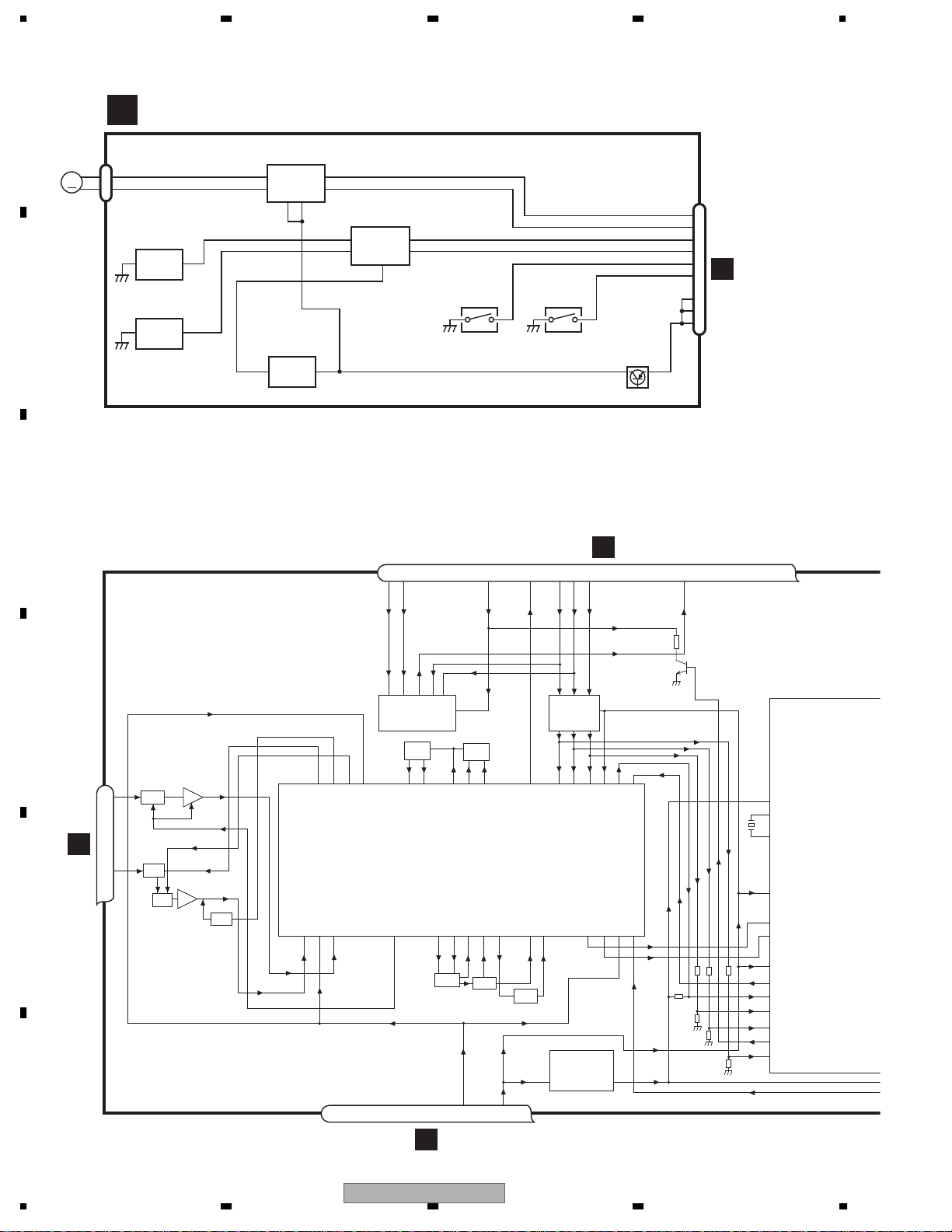
1234
A
FLAP
MOTOR
M
B
L
MAIN PCB UNIT
CN1
1
2
IC4
GP2L24B
3
GP2L24B
3
2
IC5
2
IC1
BA6288FS
3
14
45
IC2
S-812C50AMC-C3E
3
2
6
11
IC3
TC7W14FU
1
3
8
CN2
MOT0
15
MOT1
7
5
S2
HOME SW
S1
OPEN SW
Q1
2SB1185
PULSE0
PULSE1
HOMESW
OPENSW
14
13
12
10
K
9
CN2806
3
2
1
C
FM/AM TUNER UNIT
7 6 13 5 10 9 8 11 14 18 19 20 21
WC
CE2
SL
G
DI
CK
CE1
NC
DO
NCNCNC
NC
ROM_VDD
3.3V
IC 5
←
5V 3.3V
IC 4
←
3.3V 2.5V
2.5V
IC 2
2.5V
DET, FM MPX
D
AM ANT
1
ATT
G
FM ANT
3
E
F
ATT
ANT adj
FMRF
FMRF
RF adj
RFGND
212 1522 16 4 17
IC 3 EEPROM
OSCGND
5.0V
OSC
MIXER, IF AMP
DGND
AUDIOGNDNCVCC
IC 1
3.3V
T51
LPF
CF52
CF51
VDD_3.3
28
G
AVIC-D1/UC
1234
Page 29
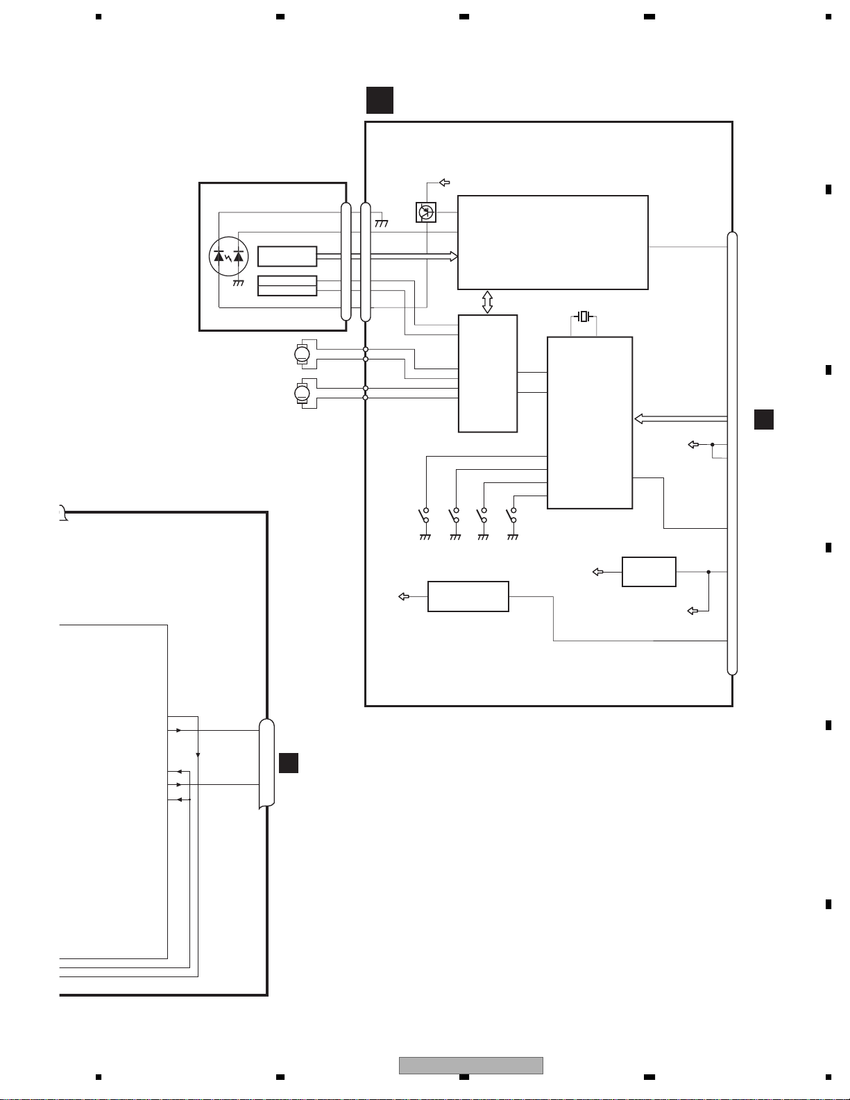
O
OR
E
OCUS ACT.
.
5678
PICKUP UNIT
(P10)(SERVICE)
LASER
DIODE
HOLOGRAM
UNIT
F
TRACKING ACT
NIT
M
DIOD
M1
SPINDLE
MOTOR
M2
LOADING/CARRIAGE
MOTOR
F
CD CORE UNIT(S10.1)
V3R3D
A
CN101
LD-
15
15
MD
FOP
TOP
LD+
5
1
4
14
Q101
5
AC,BD
E,F
FOP
1
TOP
4
14
M
M
142
LD
143
PD
RF AMP, CD DECODER,
MP3 AND WMA DECODER,
DIGITAL SERVO/DATA PROCESSOR
FD,TD
SD,MD
12
FOP
13
TOP
CD
DRIVER
16
SOP
SOM
LCOP
CONT
LCOM
IC 301
BA5835FP
LOEJ
15
18
17
IC 201
UPD63763GJ
MICRO
COMPUTER
53
22
LOEJ
9
47
CONT
32
12EJ
31
8EJ
30
DSCSNS
97
HOME
X701
1312
X1
IC 701
PE5454B
X2
VDCONT
LOUT
49
31
CN901
LOUT
BRST,BRXEN,BSRQ
BDATA,BSCK
VD
VD
10
CN1301
3
4
B
G
C
IC 2
2.5V
DET, FM MPX
Rch
Lch
VDCONT
19
S903
DSCSNS
S901
HOME
1
VD2
3V REGULATOR
3VDD
S-812C33AUA-C2N
VDD
VDD
2
VD2
5
2
D
3
IC 703
V3R3D
S904
S905
12EJ
8EJ
3
IC 203
NJM2885DL1-33
3.3V REGULATOR
24
G
23
E
F
56
AVIC-D1/UC
7
8
29
Page 30
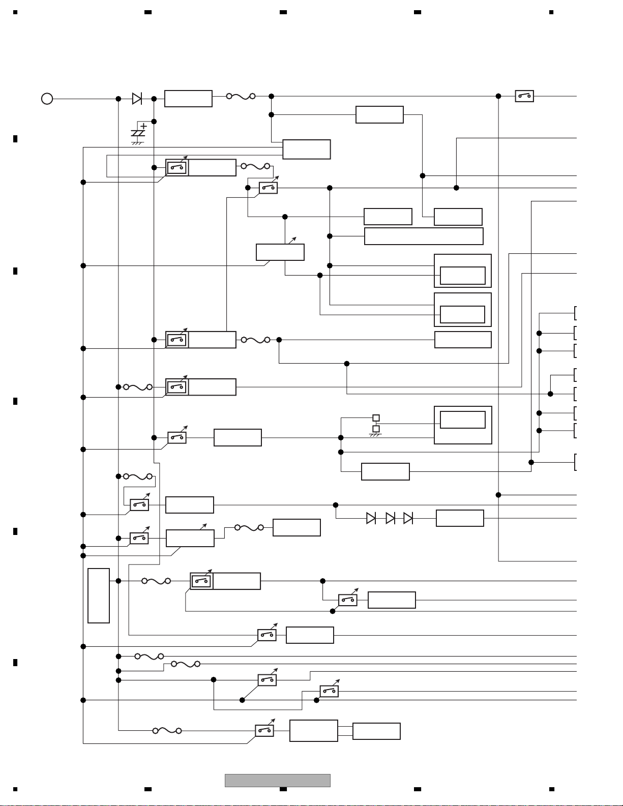
1234
A
A
V
m
0
4
0
)
m
- Power supply system figure
A
B
14.4V
B.U (CC)
BUP
13.8V
0.70W typ
5.0V Reg
3.3V D/D
[DRAMPW and CCON]
Max 1880mA
BUPV
typ 47mA
(Max 110mA)
FU1840
0.25A
FU802
2.5A
SD3V
Max 0.62W
Max 880mA
[CCON]
Max 40mA
(typ 25mA)
[CCD5]
2.5V Reg
VDD5
0.27mA
SYS µ-com
Max 580mA
CCD3
(Max 420mA)
CCD2.5
3.3V Reg
400mA
280mA
CCD3 2mA
CCD2.5 660mA
SRAM3
Max 110mA
0.1mA (Max 60mA)
SDRAM SRAM
ASIC, ROM
GDC : outside
inside
[IPPWR]
0.1mA (Max 60mA)
Max 180mA 3.3 ± 0.1
7.7m
24m
typ 4.5
300
20
11mA
AD5
V833 : outside
inside
Reference
LPF, SW
22mA
3.3V Reg
VD2
DAC
57mA
15mA
VCC5 ± 0.25V (Max 400mA)
DVD8 ± 0.4V (Max 1600mA)
typ 103mA (Max 1
11mA
30mA
43mA
28mA
15mA
17mA
VDORA33
typ 172mA (Max 2
typ 20mA (Max 60mA
typ 200mA (Max 1000mA)
typ 200
CCD3 24mA
CCD2.5 220mA
FU803
1A
C
5V D/D
[CCON]
FU1823
4A
Max 550mA
8.0V D/D
200mA (Max 1600mA)
Max 493mA
CCD5
DVD8
CCD5
[CCON]
Max 1.38W
8.5V Reg
AV85 234mA
[CCON]
D
E
FU1900
1A
[SYSPWR]
[CCON]
FU1920
1.75A
1.85W
8.5V Reg
8-12V Reg
[FANUP]
[VDCONT]
VDORA85
FU1880
0.5A
8.3V D/D
275mA (Max 340mA)
Fan Motor
VD
20mA
CCV5
AU4.7
Max 201mA
5.0V Reg
5.6V Reg
POWER AMP
FU1821
2A
FU1830 1A
PWRFL
PWRVI
[SWACPW]
[ILMPW]
F
30
1234
FU1820
2A
[MOTPW]
AVIC-D1/UC
[CD3VON]
5.6V Reg
DRIVER
SWAC56
[FLAPILM]
Flap Motor
Max 95mA
Page 31

WR]
7.7mA
24mA
5678
A
IP-BUS
232C Driver
mA (Max 60mA)
180mA 3.3 ± 0.1V
typ 4.5mA
300mA
200mA
57mA
E. Volume
15mA
11mA
Guide MIX
30mA
75Ω Driver
43mA
NTSC Enc.
28mA
15mA
Video ISO
17mA
p 103mA (Max 140mA)
2mA
RA33
p 172mA (Max 200mA)
GPS Unit
SRAM
DRAGON
A/D Con.
DVD Core Unit
VDD5
DVD8
IP ISO
VSEL
Gyro, G-sensor
TUNER
ROM
RF
PLL
B
C
D
0mA (Max 60mA)
A (Max 1000mA)
typ 200mA
CD Core Unit
VDD5
VD 8.3V
VD2 5.6V
20mA
40mA
[MEMOLED]
AVIC-D1/UC
56
7
Max 45mA
[MFLPW]
[SWACPW]
Monitor µ-com
Touch Panel
Remote control sensor
Back Light
Picture
Key LED
8
E
F
31
Page 32

1234
G
L
W
R
N
r
3.2 OVERALL CONNECTION DIAGRAM
Note: When ordering service parts, be sure to refer to " EXPLODED VIEWS AND PARTS LIST" or
"ELECTRICAL PARTS LIST".
A
FAN
MOTOR
G
SYSTEM UNIT
J
PANEL PCB
1/3
AUDIO
G
SYSCOM, VIDEO, I/F
2/3
G
P/S
3/3
G
B
MECHANISM
C
F
CD
MODULE
(S10.1AACA)
A
CC UNIT
1/6
P/S
A
CO
Wi
CPU, ASIC, SDRAM
2/6
C
D E
DVD
MECHANISM
D
E
MODULE
(MS3)
TOUCH PANEL
A
GRAPHIC
3/6
A
ROM, SRAM, BUS-BUFFER
4/6
A
MAIN, CC CORE I/F
5/6
A
GPS, SENSOR, VIDEO, I/F
6/6
A
B
K
LCD PANEL
I
KEYBOARD PCB
H
MONITOR PCB
F
32
1234
AVIC-D1/UC
Page 33

5678
WIRED
REMOTE
CONTROLLER
FM/AM
ANTENNA
A
R
CORD ASSY
Wired Remote
ANTENNA IN
FM/AM TUNER UNIT
EXTERNAL
IN/OUT
XM TUNER
AV
IN/OUT
POWER
SUPPLY
B
SUB WOOFER and NON FADER OUTPUT
CORD ASSY
C
etc.
B
GPS UNIT
K
GPS IN
CONNECTOR UNIT
GPS
ANTENNA
ASSY
IP-BUS
IN
AV-BUS
IN
IP-BUS
AV-BUS
D
E
L
MAIN PCB UNIT
56
AVIC-D1/UC
F
7
8
33
Page 34

1234
3.3 CC UNIT (P/S)
A
B
A
5/6
A
CC UNIT (P/S)
1/6
>
>
C
6/6
A
D
E
F
1/6
A
34
1234
AVIC-D1/UC
Page 35

5678
NOTE :
Symbol indicates a resistor.
No differentiation is made between chip resistors and
discrete resistors.
Symbol indicates a capacitor.
No differentiation is made between chip capacitors and
discrete capacitors.
The > mark found on some component parts indicates
the importance of the safety factor of the part.
Therefore, when replacing, be sure to use parts of
identical designation.
Decimal points for resistor
and capacitor fixed values
are expressed as :
←
2.2 2R2
←
0.022 R022
A
B
CN1802
3/3
G
C
D
56
AVIC-D1/UC
7
2SA1385-ZS1
E
F
1/6
A
8
35
Page 36

1234
A-a
A-b
A-a
A-b
A-b
A-a
3.4 CC UNIT (CPU, ASIC, SDRAM)(GUIDE PAGE)
Large size
A
B
A-a
A-a
SCH diagram
A-b
A-a
A-a
A-b
Guide page
CC UNIT (CPU, ASIC, SDRAM)
2/6
A
Detailed page
A-b
2/6
5/6
A
C
D
E
F
2/6
A
36
1234
AVIC-D1/UC
3/6
A
Page 37

5678
CN601
C
5/6
A
A-b
2/6
5/6
A
A
B
C
D
E
4/6
A
F
56
AVIC-D1/UC
2/6
A
7
8
37
Page 38

A
B
A-b
1234
2/6
1
5/6
A
C
A-b
A-a
A-a
D
E
F
A-a
38
CC UNIT (CPU, ASIC, SDRAM)
2/6
A
2/6
AVIC-D1/UC
1234
Page 39

5678
A
2
A-b
2/6
B
3/6
A
A-b
A-a
A-a
C
D
E
56
AVIC-D1/UC
F
A-a
2/6
7
8
39
Page 40

1234
A
5/6
A
B
C
A-b
A-a
D
CN601
E
C
F
A-b
40
2/6
1234
1
AVIC-D1/UC
Page 41

5678
A
B
4/6
A
C
A-b
A-a
D
E
56
AVIC-D1/UC
F
2
7
A-b
8
2/6
41
Page 42

1234
3.5 CC UNIT (GRAPHIC)(GUIDE PAGE)
A
CC UNIT (GRAPHIC)
3/6
A
B
2/6
A
C
A-a
3/6
4/6
A
D
E
F
42
A
3/6
AVIC-D1/UC
1234
Page 43

5678
A-b
3/6
A
B
5/6
A
C
D
E
F
56
AVIC-D1/UC
3/6
A
7
8
43
Page 44

A
B
A-b
1234
3/6
1
C
A-b
A-a
A-a
D
E
F
A-a
44
CC UNIT (GRAPHIC)
3/6
A
2/6
A
3/6
1234
AVIC-D1/UC
Page 45

5678
A
2
3
A-b
3/6
B
A-b
A-a
A-a
C
D
E
4/6
A
AVIC-D1/UC
56
F
A-a
3/6
7
8
45
Page 46

1234
A
5/6
A
B
C
A-b
A-a
D
E
F
A-b
46
3/6
1234
1
AVIC-D1/UC
Page 47

5678
A
B
A-b
A-a
C
D
E
2
AVIC-D1/UC
56
F
3
7
A-b
8
3/6
47
Page 48

1234
3.6 CC UNIT (ROM, SRAM, BUS-BUFFER)
A
B
C
2/6
A
D
E
F
4/6
A
48
1234
AVIC-D1/UC
Page 49

5678
A
CC UNIT (ROM, SRAM, BUS-BUFFER)
4/6
A
B
C
A
3/6
A
D
E
5/6
F
56
AVIC-D1/UC
4/6
A
7
8
49
Page 50

1234
3.7 CC UNIT (MAIN, CC CORE I/F)
A
A
B
C
CC UNIT (MAIN, CC CORE I/F)
5/6
A
2/6
A
AUDIO SIGNAL
A
4/6
D
3/6
A
E
F
50
A
5/6
AVIC-D1/UC
1234
Page 51

5678
A
1/6
A
B
C
A
6/6
A
A
D
A
E
56
AVIC-D1/UC
F
5/6
A
7
8
51
Page 52

1234
3.8 CC UNIT (GPS, SENSOR, VIDEO, I/F)
A
CC UNIT (GPS, SENSOR, VIDEO, I/F)
6/6
A
R
B
5/6
A
C
A-a
6/6
>
R
D
1/6
A
S
E
F
R
V
V
R
S
S
R
V
S
52
A
6/6
CN5002
H
AVIC-D1/UC
1234
Page 53

5678
CN461
B
A-b
6/6
V
COMPOSIT VIDEO SIGNAL
R
RGB SIGNAL
S
SYNC SIGNAL
A
AUDIO SIGNAL
A
B
A
V
V
V
2/3
G
CN1701
C
D
E
A
V
CN2804
K
AVIC-D1/UC
56
F
6/6
A
7
8
53
Page 54

A
B
A-b
1234
6/6
>
1
C
A-b
A-a
A-a
D
R
E
F
A-a
54
CC UNIT (GPS, SENSOR, VIDEO, I/F)
5/6
6/6
A
A
6/6
1234
AVIC-D1/UC
Page 55

5678
A
A-b
6/6
R
V
S
B
S
R
S
V
R
V
CN5002
H
C
A-b
A-a
A-a
R
S
D
E
1/6
A
AVIC-D1/UC
56
F
A-a
6/6
7
8
55
Page 56

1234
A
B
V
V
A
COMPOSIT VIDEO SIGNAL
RGB SIGNAL
SYNC SIGNAL
AUDIO SIGNAL
S
R
V
C
A
2/3
G
CN1701
V
A-b
A-a
D
CN461
B
E
F
A-b
56
6/6
1
AVIC-D1/UC
1234
Page 57

CN1701
5678
A
B
C
A-b
A-a
A
V
CN2804
D
K
E
56
AVIC-D1/UC
F
A-b
6/6
7
8
57
Page 58

1234
3.9 GPS UNIT (GUIDE PAGE)
A
GPS ANTENNA
B
C
B-a
D
E
6/6
A
CN551
F
58
B
AVIC-D1/UC
1234
Page 59

5678
B-b
B
A
GPS UNIT
B
C
D
E
F
56
AVIC-D1/UC
B
7
8
59
Page 60

A
B
B-b
1234
1
2
3
4
5
C
B-b
A-a
B-a
D
E
F
B-a
60
GPS ANTENNA
AVIC-D1/UC
1234
Page 61

5678
A
6
7 8
B-b
B
B-b
A-a
B-a
C
D
E
6/6
A
CN551
56
AVIC-D1/UC
F
B-a
7
8
61
Page 62

1234
A
GPS UNIT
B
B
C
B-b
B-a
D
E
F
B-b
62
1
1234
2
AVIC-D1/UC
3
4
5
Page 63

5678
A
B
B-b
B-a
C
D
E
6
7 8
AVIC-D1/UC
56
F
B-b
7
8
63
Page 64

1234
3.10 DVD CORE UNIT(MS3R)(GUIDE PAGE)
A
B
PICKUP UNIT(SERVICE)
V
C-a
C
F
F
T
T
1
D
E
M3 SPINDLE MOTOR
CXM1308
CARRIAGE MOTOR
CXC4314
M2
4
T
T
F
F
3
5
F
T
2
sense
D
F
M1 LOADING MOTOR
CXC4659
AVIC-D1/UC
64
C
1234
E
Page 65

5678
A
C-b
B
DVD CORE UNIT (MS3R)
C
A
CN2
C
2/6
D
E
: The power supply is shown with the marked box.
AVIC-D1/UC
56
F
AB
7
8
C
65
Page 66

A
B
C-b
1234
1
C
1
C-b
A-a
C-a
D
E
F
C-a
66
V
F
T
F
T
PICKUP UNIT(SERVICE)
AVIC-D1/UC
1234
Page 67

5678
A
1
2
C-b
B
C
5
F
2
sense
D
TTF
T
F
4
3
E
C-b
A-a
C-a
CXC4659
M1 LOADING MOTOR
D
E
M3 SPINDLE MOTOR
CXM1308
AVIC-D1/UC
56
M2
CARRIAGE MOTOR
CXC4314
7
8
F
C-a
67
Page 68

1234
A
2/6
CN2
A
B
DVD CORE UNIT (MS3R)
C
C
C-b
C-a
D
E
F
C-b
68
1
AVIC-D1/UC
1234
Page 69

2/6
A
5678
A
CN2
B
: The power supply is shown with the marked box.
C
C-b
C-a
D
E
F
1
2
AVIC-D1/UC
56
C-b
7
8
69
Page 70

1234
- Waveforms
Note:1. The encircled number denote measuring pointes in the circuit diagram.
2. Reference voltage VHALF : 1.65V(TD1,FD1,CRGDRV)
: 2V Center(ANAMONI1)
A
1 RFOUT 0.2V/div. 0.1µs/div.
CDRF
B
2 TD 0.5V/div. 100µs/div.
0.2V/div. 100µs/div.
Interval
C
VHALF→
In this waveform, it is seeing on the GND standard.
Offset of 1.65V or 2V is put in.
1 RFOUT
0.2V/div. 0.1µs/div.
DVDRF DVDRF(BD1mm)
VHALF→VHALF→
2 TD 0.5V/div. 100µs/div.
Interval FWD
VHALF→ VHALF→
1 RFOUT
VHALF→
2 TD
Interval REV
0.5V/div. 100µs/div.
2 CH1: TD
0.5V/div.5ms/div. 2 CH1: TD
3 CH2: COP-COM 2.0V/div.5ms/div.
Traverse501FWD
VHALF→
D
VHALF→
E
0.5V/div.5ms/div. 2 CH1: TD
3 CH2: COP-COM 2.0V/div.5ms/div.
Traverse501REV
VHALF→
VHALF→
0.5V/div.5ms/div.
3 CH2: COP-COM 2.0V/div.5ms/div.
Traverse5000FWD
VHALF→
VHALF→
F
70
1234
AVIC-D1/UC
Page 71

5678
2 CH1: TD
0.5V/div.5ms/div.
3 CH2: COP-COM 2.0V/div.5ms/div.
Traverse5000REV
VHALF→
VHALF→
2 TD
0.5V/div.20ms/div.
Play TD
VHALF→
5 FD
Focus jamp L 0
0.5V/div.500µs/div.
→ L1
2 TD
0.5V/div.500µs/div.
Multi 32FWD
VHALF→
4 CRGPRV
0.5V/div. 100µs/div.
ID search Insaide
VHALF→
5 FD
0.5V/div.500µs/div.
Focus jamp L1
→ Outside
→ L 0
2 TD
0.5V/div.500µs/div.
Multi 32REV
VHALF→
5 FD 0.5V/div. 1ms/div.
Focus close
VHALF→
5 FD
0.5V/div.20ms/div.
Play TD
A
B
C
VHALF→
VHALF→
VHALF→
D
E
56
AVIC-D1/UC
F
7
8
71
Page 72

1234
3.11 COMPOUND UNIT(A) AND COMPOUND UNIT(B)
COMPOUND UNIT(A)
A
D
B
C
C
CN1202
6
5
DISC SENS
4
CSN1069
3
CSN1069
2
CSN1069
1
8cm
12cm
R1298
0R0
Q1299
CPT231SCTD
DISC SENS
S1203
S1202
S1201
R1299
0R0
S1204
CSN1070
8cm
CSN1070
S1205
COMPOUND UNIT(B)
E
CLAMP
D
C
E
F
D E
72
1234
AVIC-D1/UC
Page 73

5678
3.12 PU UNIT(REFERENCE)
Short round
Iop78
IC1
C6
L1
L3
65LD78LD
1715
C1
LDGND
16
MDA
98
C8
C9
MDC
A
SW
12
Vcc
13
GND
14
V r
C7
R1C5 Short round
up
Top View
MDA
L6
RF+
LC
GND
Vcc
GND
Im/ 2
Im
B1
B2
RF-
B3
B4
C
R2
Im/ 2
1
2
3
4
5
6
7
L2
C4
Vshf : 4V
C2C3
VR1/ 78RmdVmda
L4
Iop65
C10TH1
78LD
65LD
LDGND
65MD
65MDGVR2/ 65Rmd
78MD
78MDG
MDG
RF+
Vref : 2.5V
GND
TEMP
Vcc
SW
24
Ishf
23
26
25
07
08
05
C
06
CN1101
09
B1
16
B2
15
RF-
14
B3
13
12
B4
11
C
10
22
21
20
19
18
A
17
NC
27
T-
02
A
B
C
D
E
56
AVIC-D1/UC
T+
01
F-
03
F+
04
F
7
8
73
Page 74

1234
Y
3.13 CD MECHANISM MODULE(GUIDE PAGE)
A
F-a
PICKUP UNIT(P10)(SERVICE)
B
F
T
C
S
%
F
T
F
T
T
F
F
T
F
F
T
T
#
@
C
D
3
2
1
E
M1 CXC4440
SPINDLE MOTOR
M2 CXB8933
LOADING
/CARRIAGE
MOTOR
S
S
C
C
T
9
F
0
F
F
T
T
CD DRIVER
$
S
7
C
8
4
5
S
C
S
C
T
F
F
74
1234
AVIC-D1/UC
Page 75

5678
A
F-b
SWITCHES:
CD CORE UNIT(S10.1)
ras
!
S901:HOME SWITCH..........ON-OFF
S903:DSCSNS SWITCH......ON-OFF
S904:12EJ SWITCH.............ON-OFF
S905:8EJ SWITCH...............ON-OFF
The underlined indicates the switch position.
SIGNAL LINE
F
FOCUS SERVO LINE
T
TRACKING SERVO LINE
C
CARRIAGE SERVO LINE
S
SPINDLE SERVO LINE
CD CORE UNIT(S10.1)
F
B
TYPE_A/D
MICRO COMPUTER
PE5454B
SRAMLEVEL2
SRAMLEVEL1
SRAMLEVEL0
3V REGULATOR
3.3V REGULATOR
C
D
2/3
G
CN1301
6
E
^
&
AVIC-D1/UC
56
F
F
7
8
75
Page 76

A
F-b
1234
1
2
B
C
F-b
F-a
A-a
F
T
C
S
#
@
%
T
T
F
F
D
T
T
E
F
F
T
TFF
F
F-a
76
1234
PICKUP UNIT(P10)(SERVICE)
AVIC-D1/UC
Page 77

5678
A
2
3 4
5 6
F-b
B
4
C
7
$
S
T
8
C
T
C
S
S
CD DRIVER
F-b
F-a
A-a
D
C
9
5
F
T
F
0
F
E
2
3
1
S
S
M1 CXC4440
SPINDLE MOTOR
C
AVIC-D1/UC
56
C
LOADING
/CARRIAGE
M2 CXB8933
7
MOTOR
8
F
F-a
77
Page 78

1234
A
B
CD CORE UNIT(S10.1)
3.3V REGULATOR
F
SIGNAL LINE
FOCUS SERVO LINE
TRACKING SERVO LINE
CARRIAGE SERVO LINE
C
SWITCHES:
CD CORE UNIT(S10.1)
S901:HOME SWITCH..........ON-OFF
S903:DSCSNS SWITCH......ON-OFF
S904:12EJ SWITCH.............ON-OFF
S905:8EJ SWITCH...............ON-OFF
F-b
F-a
D
F
The underlined indicates the switch position.
SPINDLE SERVO LINE
T
S
C
E
F
F-b
78
!
ras
1
2
AVIC-D1/UC
1234
Page 79

5678
2/3
G
CN1301
6
A
B
SRAMLEVEL2
3V REGULATOR
SRAMLEVEL0
SRAMLEVEL1
^
&
C
F-b
F-a
D
E
PE5454B
MICRO COMPUTER
TYPE_A/D
F
2
3 4
AVIC-D1/UC
56
5 6
7
8
F-b
79
Page 80

1234
- Waveforms Note : 1. The encircled numbers denote measuring points in the circuit diagram.
2. Reference voltage REFO1(1.65V)
A
1 DSCSNS
2 8SNS
3 12SNS
4 LOEJ
12 cm CD Loading operation
5V/div
5V/div
5V/div
5V/div
500ms/div
1 DSCSNS
5 CLCONT
4 LOEJ
6 VD
12 cm CD Loading operation 8 cm CD Loading operation
5V/div
5V/div
5V/div
10V/div
500ms/div
1 DSCSNS
2 8SNS
3 12SNS
4 LOEJ
5V/div
5V/div
5V/div
5V/div
500ms/div
Ref.:
GND
Mode:
Normal
B
7 SIN
8 CIN
9 TIN
12 cm CD-DA setup operation after loading 12 cm CD-ROM(3 sessions) setup operation
Ref.:
C
REFO
Mode:
Normal
0 FIN
! RFOK
7 SIN
12 cm CD-DA Source On setup operation
D
1V/div
500mV/div
500mV/div
200mV/div
2V/div
2V/div
2s/div
500ms/div
Ref.:
GND
Mode:
Normal
7 SIN
8 CIN
9 TIN
12 cm CD-ROM(1 session) setup operation
after loading
Ref.:
REFO
Mode:
Normal
@ TE
# FE
Source On setup operation CD-DA Play operation
1V/div
500mV/div
500mV/div
500mV/div
500mV/div
1s/div
200ms/div
Ref.:
GND
Mode:
Normal
7 SIN
8 CIN
9 TIN
after loading
Ref.:
REFO
Mode:
Normal
# FE
0 FIN
@ TE
9 TIN
1V/div
500mV/div
500mV/div
500mV/div
500mV/div
500mV/div
500mV/div
2s/div
20ms/div
Ref.:
REFO
Mode:
Normal
# FE
0 FIN
E
@ TE
9 TIN
CD-ROM play operation(Regular track Jump)
Ref.:
REFO
Mode:
Normal
F
80
500mV/div
500mV/div
500mV/div
500mV/div
1234
20ms/div
Ref.:
REFO
Mode:
Normal
$ MDX
7 SIN
Spindle waveform during play operation Spindle waveform during play operation
Ref.:
REFO
Mode:
Normal
1V/div
200mV/div
50ms/div
Ref.:
REFO
Mode:
Normal
$ MDX
7 SIN
(Wider)
Ref.:
REFO
Mode:
Normal
2V/div
1V/div
5µs/div
AVIC-D1/UC
Page 81

5678
0 FIN
# FE
Focus Search waveform
Ref.:
REFO
Mode:
TEST
% RFAGC
@ TE
9 TIN
4 Tracks Jump waveform 32 Tracks Jump waveform
Ref.:
REFO
Mode:
TEST
500mV/div
500mV/div
1V/div
500mV/div
500mV/div
200ms/div
500µs/div
@ TE
% RFAGC
500mV/div
500mV/div
2ms/div
% RFAGC
@ TE
9 TIN
Track Open waveform 1 Track Jump waveform
Ref.:
REFO
Mode:
TEST
% RFAGC
@ TE
9 TIN
10 Tracks Jump waveform
Ref.:
REFO
Mode:
TEST
1V/div
500mV/div
500mV/div
1ms/div
Ref.:
REFO
Mode:
TEST
% RFAGC
@ TE
9 TIN
Ref.:
REFO
Mode:
TEST
1V/div
500mV/div
500mV/div
1V/div
500mV/div
500mV/div
500µs/div
A
B
2ms/div
C
% RFAGC
@ TE
8 CIN
7 SIN
Search operation(Outter to Inner)
Ref.:
REFO
Mode:
Normal
1 DSCSNS
5 CLCONT
4 LOEJ
12 cm CD Eject operation
Ref.:
GND
Mode:
Normal
1V/div
1V/div
500mV/div
2V/div
5V/div
5V/div
5V/div
200ms/div
500ms/div
^ LOUT
& ROUT
Analog audio waveform
Ref.:
AGND
Mode:
Normal
1 DSCSNS
2 8SNS
3 12SNS
4 LOEJ
8 cm CD Eject operation
Ref.:
GND
Mode:
Normal
1V/div
1V/div
5V/div
5V/div
5V/div
5V/div
200µs/div
500ms/div
1 DSCSNS
2 8SNS
3 12SNS
4 LOEJ
12 cm CD Eject operation
Ref.:
GND
Mode:
Normal
7 SIN
8 CIN
9 TIN
CD-DA >> CD-ROM mode change(Band key)
Ref.:
REFO
Mode:
Normal
5V/div
5V/div
5V/div
5V/div
1V/div
500mV/div
500mV/div
500ms/div
500ms/div
D
E
56
AVIC-D1/UC
F
7
8
81
Page 82

1234
7 SIN
8 CIN
A
9 TIN
CD-ROM >> CD-DA mode change(Band key)
Ref.:
REFO
Mode:
Normal
B
C
1V/div
500mV/div
500mV/div
500ms/div
% RFAGC
9 TIN
@ TE
0 FIN
Black dot(800µm) during play
Ref.:
REFO
Mode:
Normal
1V/div
1V/div
1V/div
1V/div
500µs/div
D
E
F
82
1234
AVIC-D1/UC
Page 83

5678
A
B
C
D
E
56
AVIC-D1/UC
F
7
8
83
Page 84

1234
3.14 SYSTEM UNIT (AUDIO)
A
3/3
G
G
2/3
B
2/3
G
A
A
C
D
A
A
A
A
A
A
A
A
A
A
A
A
E
2/3
G
F
1/3
G
84
1234
AVIC-D1/UC
Page 85

5678
A
AUDIO SIGNAL
G
SYSTEM UNIT (AUDIO)
1/3
A
A
A
A
A
A
AA
A
A
A
A
A
A
A
A
A
A
2/3
G
3/3
G
B
C
D
56
AVIC-D1/UC
A
A
1/3
G
7
8
E
F
85
Page 86

1234
R
3.15 SYSTEM UNIT (SYSCOM, VIDEO, I/F)(GUIDE PAGE)
A
B
V
V
V
G-a
V
V
V
2/3
1/3
G
A
A
A
V
V
V
V
V
V
A
V
V
A
V
C
D
6/6
A
CN605
A
V
V
E
V
A
SYSTEM CONTROLLE
F
86
G
2/3
AVIC-D1/UC
1234
Page 87

5678
G-b
CN901
F
A
V
A
V
V
V
A
A
A
A
2/3
SYSTEM UNIT (SYSCOM, VIDEO, I/F)
2/3
G
V
COMPOSIT VIDEO SIGNAL
A
AUDIO SIGNAL
>
V
V
V
A
A
A
A
>
B
C
A
EM CONTROLLER
J
CN5901
D
3/3
G
E
56
AVIC-D1/UC
F
2/3
G
7
8
87
Page 88

A
B
G-b
1234
2/3
1
A
V
V
A
V
2
1/3
G
A
A
A
C
G-b
A-a
G-a
V
V
V
V
V
V
D
V
V
V
V
V
V
E
F
G-a
88
2/3
AVIC-D1/UC
1234
Page 89

5678
R
3
G-b
2/3
A
SYSTEM CONTROLLE
B
C
G-b
A-a
G-a
D
E
V
V
A
V
A
6/6
A
CN605
56
AVIC-D1/UC
F
G-a
2/3
7
8
89
Page 90

1234
A
VVV
A
A
A
V
A
>
J
CN5901
B
>
SYSTEM UNIT (SYSCOM, VIDEO, I/F)
COMPOSIT VIDEO SIGNAL
AUDIO SIGNAL
A
V
2/3
G
C
A
G-b
G-a
D
E
V
V
A
A
A
CN901
F
A
F
G-b
90
2/3
1
2
AVIC-D1/UC
1234
Page 91

5678
A
3/3
G
B
G-b
G-a
C
D
E
NTROLLER
AVIC-D1/UC
56
F
3
7
G-b
8
2/3
91
Page 92

1234
3.16 SYSTEM UNIT (P/S)
A
A
A
B
1/3
G
C
D
>
>
>
>
2/3
G
E
>
>
F
CN801
1/6
A
3/3
G
92
1234
AVIC-D1/UC
Page 93

5678
>
FAN MOTOR
CXM1320
G
PTZ27(B)
A
AUDIO SIGNAL
SYSTEM UNIT (P/S)
3/3
A
B
C
>
PTZ27(B)
A
A
D
E
>
AVIC-D1/UC
56
F
3/3
G
7
8
93
Page 94

1234
S
7
3.17 MONITOR PCB (GUIDE PAGE)
A
H-a
POWER SUPPLY
(
B
1 2
4
DIMMER
3
5
6
C
TEMPERATURE
SENSOR
V
D
A
6/6
CN701
S
V
8
R
!
E
⁄
¤
)
F
: The power supply is shown with the marked box.
Monitor Adjustment PCB(GGF1416)
H
94
1234
AVIC-D1/UC
Page 95

5678
IMMER
H-b
MONI_PANEL UNIT
Consists of
MONITOR PCB
KEYBOARD PCB
PANEL PCB
MONITOR PCB
H
LCD PANEL
A
B
7
6
TOUCH PANEL
C
@
Y/C
Separation
OSD
Interface
R
S
P in P IC
I
CN5700
V
D
9
R
^
%
*
LCD PANEL
$
E
&
Multi
Processing
P in P
Video
TFT
Controller
R
#
R
0
56
AVIC-D1/UC
R
: RGB Signal
S
: Sync Signal
V
: Composite Video Signal
7
F
H
8
95
Page 96

1234
6
A
B
C
H-b
DIMMER
5
V
4
H-b
A-a
H-a
D
1 2
3
POWER SUPPLY
(
E
SENSOR
TEMPERATURE
F
H-a
96
1234
AVIC-D1/UC
Page 97

5678
A
1
2
⁄
¤
)
3
H-b
B
C
Monitor Adjustment PCB(GGF1416)
H-b
A-a
H-a
D
E
!
R
V
A
6/6
CN701
8
S
AVIC-D1/UC
56
: The power supply is shown with the marked box.
F
H-a
7
8
97
Page 98

1234
N
LCD PANEL
A
TOUCH PANEL
C
I
MONITOR PCB
H
B
MONI_PANEL UNIT
Consists of
MONITOR PCB
KEYBOARD PCB
C
PANEL PCB
H-b
H-a
D
P in P IC
S
R
E
F
H-b
98
7
6
IMMER
AVIC-D1/UC
1234
Page 99

5678
P
in
P
IC
I
CN5700
LCD PANEL
A
$
*
^
R
0
%
R
&
: RGB Signal
: Sync Signal
RSV
B
: Composite Video Signal
C
R
9
#
Controller
TFT
H-b
H-a
D
V
@
Video
Multi
P in P
Processing
Y/C
Separation
OSD
Interface
E
1
2
AVIC-D1/UC
56
F
3
7
8
H-b
99
Page 100

1234
G
T
G
C585
0
C585
7
C585
38
C585
7
C590
2
C590
6
C590
7
C0
S2
GOUT
G
C0
OL
COM
G
C0
CX
1
G
- Waveforms
A
B
C
CH1 : I
CH2 : I
CH1 : I
CH2 : I
1 Pin 1
1 Pin
1 Pin
1 Pin
CH3 : I
CH4 : I
CH3 : I
The encircled number denote measuring pointes in the circuit diagram.
1 Pin
1 Pin 4
1 Pin
CH1 : CSYN
CH2 : CVB
CH1 : CSYN
CH2 : P
CH3 :
CH4 : V
CH3 : V
CH4 : V
D
CH1 : AN
CH3 : V
CH2 : GOU
E
F
CH1 : CSYN
CH2 :
CH3 : STH
CH4 : V
100
1234
AVIC-D1/UC
 Loading...