

Philips FWC-550 Service manual

Service
Service
Service
Service
FW-C550
A01 - 156
Service
Product Service Group CE Audio
Service Information
Already published Service Informations :
CORRECTION TO SERVICE MANUAL
*Page 1-3 : The correct Tuner FM Aerial input for /37 version
*Page 9-5 : Due to some error, the Tape Adjustment & Check Table
*Correction of Mechanical & Accessories parts list (Page 13-2):
Change 0151 3139 118 16080 Cover Cassette Left
*Correction of circuit drawing and parts list for Front Control
Board:
Change 6842 9322 172 75676 LED VS LTL-1CHKFK
*Correction of circuit drawing and parts list for Front Display
Board:
Add 2508 3198 024 44730 47nF 50V
Change 3407 4822 051 20109 10R 5% 0,1W
*Correction of circuit drawing and parts list for AF9 Board:
Add 2210 4822 126 13879 220nF +80/-20% 16V
Change 2208 4822 126 13879 220nF +80/-20% 16V
Delete 4102, 4118
should be 300ohm click fit.
is enclosed.
0152 3139 118 16090 Cover Cassette Right
0153 3139 114 72820 Lens Cassette Left
0154 3139 114 72830 Lens Cassette Right
1503 3139 110 35880 FFC Foil 15P/180/15P BD
3408 4822 051 20109 10R 5% 0,1W
3410 4822 051 20109 10R 5% 0,1W
3411 4822 051 20109 10R 5% 0,1W
3535 4822 051 20109 10R 5% 0,1W
3536 4822 051 20109 10R 5% 0,1W
3570 4822 051 20109 10R 5% 0,1W
3571 4822 051 20109 10R 5% 0,1W
5403 2422 543 01069 RES XTL 32,768kHz
6420 9322 167 73676 LED VS LTL-4221NLC-KA
!
3821 4822 052 10109
4148 4822 051 30008 0R Jumper 0603
4151 4822 051 30008 0R Jumper 0603
4152 4822 051 30008 0R Jumper 0603
2626 4822 124 40769 4,7uF 20% 100V
3534 4822 051 30273 27k 5% 0,062W
10R 5% 0,33W
*Correction of circuit drawing and parts list for MMPWR 100W
Module (L/R Amplifier & Supply Board):
Change 2345 2020 561 90365 100nF +80/-20% 50V
CHANGES DURING PRODUCTION
MECHANICAL & ACCESSORIES PARTS LIST (Page 13-2)
*From production week 0140 onwards the following has been
changed due to UL Requirement to use V2 material for all major
enclosure parts.
Change 0253 3139 114 74780 Panel Left (V2)
FRONT CONTROL BOARD
*From production week 0110 onwards pt.2 Board (identified by the
last digit of the 12NC - 3139 113 3446
reason new layout and circuit drawing are enclosed.
Reason : ESD solution.
FRONT DISPLAY BOARD
*From production week 0110 onwards pt.2 Board (identified by the
last digit of the 12NC - 3139 113 3447
reason new layout and circuit drawing are enclosed.
Reason : Solution for tuner-locking issue.
Add 6415 4822 130 11397 BAS316
Change 3409 4822 117 12925 47k 1% 0,063W
Delete 3405
Reason : ESD solution.
Add 2585 4822 126 13883 220pF 5% 50V
Change 2563 5322 126 11583 10nF 10% 50V
Delete 9513, 9514 Bare wires
0254 3139 114 74790 Panel Right (V2)
0255 3139 114 74800 Cover Top (V2)
0256 3139 114 74850 Panel Rear (V2)
2) is introduced. For this
2) is introduced. For this
2586 4822 126 13883 220pF 5% 50V
2587 3198 017 41050 1uF 10V
2588 4822 126 13879 220nF +80/-20% 16V
2589 3198 017 41050 1µF 10V
5408 4822 157 62552 Coil 2,2uH 5%
5409 4822 157 62552 Coil 2,2uH 5%
(P.T.O.)
15 - 01 - 2002
3139 785 30004

*From production week 0115 onwards the software of the main
processor IC (7400) has been upgrade to version 14. The new
service code is 9965 000 10407.
*From production week 0121 onwards pt.4 Board (identified by the
last digit of the 12NC - 3139 113 3434
4) is introduced. For this
reason new layout and circuit drawing are enclosed.
*From production week 0126 onwards the following has been
changed to lower ADC step from 255 to 253 so as to solve
irregularly power-up recording problem.
Add 3524 4822 051 30109 10R 5% 0,062W
Delete 4405
AF9 BOARD
*From production week 0110 onwards pt.3 Board (identified by the
last digit of the 12NC - 3139 113 3435
3) is introduced.
Reason : For process, EMC & ESD improvement.
Add 2950 4822 126 13881 470pF 5% 50V
2951 4822 126 13881 470pF 5% 50V
2952 4822 122 31765 100pF 2% 63V
2953 4822 126 13881 470pF 5% 50V
3820 4822 116 52176 10R 5% 0,5W
Change 6206 4822 130 31878 1N4003G
Delete 9614 Bare wire
*From production week 0122 onwards the following has been
changed for GSM solution.
Add 3525 4822 051 30471 470R 5% 0,062W
3526 4822 051 30471 470R 5% 0,062W
3645 4822 051 30221 220R 5% 0,062W
3646 4822 051 30221 220R 5% 0,062W
4153 4822 051 30008 0R Jumper 0603
4641 4822 051 30008 0R Jumper 0603
4642 4822 051 30008 0R Jumper 0603
Delete 3641, 3642
Reason : For EMC solution.
Add 2370 2020 561 90365 100nF +80/-20% 50V
2371 2020 561 90365 100nF +80/-20% 50V
2372 4822 126 12878 1,5nF 10% 16V
3395 4822 116 52175 100R 5% 0,5W
*From production week 0137 onwards the following has been
changed for EMC performance.
Change 2330 4822 122 33519 470pF 10% 50V
2335 4822 122 33519 470pF 10% 50V
Delete 2328, 2331
*From production week 0132 onwards the following has been
changed to solve capacitor current leakage issue.
Change 2503 4822 124 22466 1uF 20% 50V
2504 4822 124 22466 1uF 20% 50V
2511 4822 124 22466 1uF 20% 50V
2512 4822 124 22466 1uF 20% 50V
*During production pt.4 Board (identified by the last digit of the 12NC
– 3139 113 3435
4) is introduced. For this reason new layout and
circuit drawing are enclosed.
MMPWR 100W MODULE - MAINS BOARD
*During production pt.7 Board (identified by the last digit of the 12NC
- 3139 113 3433
7) is introduced. For this reason new layout and
circuit drawing are enclosed.
MMPWR 100W MODULE - L/R AMP. & SUPPLY BOARD
*From production week 0121 onwards the following has been
changed to increase Fan speed.
!
Change 3304 4822 052 10108
1R 5% 0,33W
3305 4822 116 83876 270R 5% 0,5W
3306 4822 116 83876 270R 5% 0,5W
*From production week 0121 onwards the following has been
changed for NTC sensitivity adjustment.
Add 3292 4822 116 52263 2k7 5% 0,5W
Change 6258 4822 130 34173 BZX79-B5V6
FRONT CONTROL BOARD
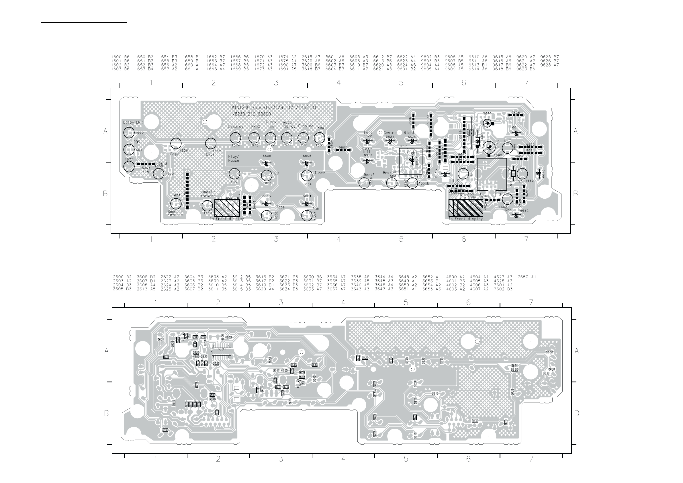
FRONT CONTROL BOARD - COMPONENT LAYOUT
This assembly drawing shows a summary of all possible versions. For components used in a specific version see schematic diagram and respective parts list.
FRONT CONTROL BOARD - CHIP LAYOUT
3139 113 3446 pt2 dd wk0116
This assembly drawing shows a summary of all possible versions. For components used in a specific version see schematic diagram and respective parts list.
3139 113 3446 pt2 dd wk0116

FRONT CONTROL BOARD - CIRCUIT DIAGRAM
This assembly drawing shows a summary of all possible versions.
For components used in a specific version see schematic diagram and respective parts list.
3139 113 3446 pt2 dd wk0116
IR-EYE BOARD - COMPONENT LAYOUT IR-EYE BOARD - CHIP LAYOUT
1600 F1
1601 H2
1602 D1
1603 H1
1650 D2
1651 C2
1652 C3
1653 C3
1654 C3
1655 C2
1656 D3
1657 D3
1658 D3
1659 D2
1661 D4
1662 C5
1663 C6
1664 C6
1665 C7
1666 C5
1668 C4
1669 C4
1670 C6
1671 D6
1672 D6
1673 D5
1674 D5
1675 D4
1690 B1
1691 A3
2600 G5
2603 G5
2604 B4
1667 C4
1660 D5
1234567
A
JOG_A
JOG_B
1690
EC16
MT14MT2
10K
3606
3607
1
2
3
5
2606
10n
2607
B
3610
150R
1651
GND-B
1650
GND-B
Gnd
Woox_A
Woox_B
Vac
DSC
9618
# 3600
470R
Max_Woox_LedShClk
+5V6
Gnd
Gnd
PLAY
3630
150R
S_fwd
Gnd
9610
Gnd Gnd
C
FE-ST-VK-N
D
E
F
G
1602
1600
FE-ST-VK-N
1
2
3
4
5
6
7
8
9
10
11
12
FE-ST-VK-N
1
2
3
4
5
6
7
8
1603
Key2
Key1
1
2
3
4
5
6
7
8
9
10
1601
FE-ST-VK-N
Tuner
Tape
1
2
3
4
5
6
7
8
GND-B
JOG_A
H
2605 B4
2623 F7
2606 B2
2607 B2
2608 C7
2613 D6
2615 A4
2620 F3
10K
10n
3611
220R
1652
1655
CD
GND-B
GND-B
3631
220R
1659
S_back
GND-B
GND-B GND-B
DBB_ShStr
IS_ShData
4600
VacJOG_B
6610
DSC
6611
6612
DBB_Led
IS_Led
6613
2624 G4
2625 G4
3600 G2
3604 A4
3605 A4
3612
270R
TAPE
3632
270R
1658
+5V6
2620
3649
3648
Gnd
Green-Led
10u
10K
3607 A2
3608 G5
3609 G4
3610 C2
3611 C3
3612 C3
Woox_A
Woox_B
3613
390R
1653
AUX
GND-B
3633
390R
1657
STOP
GND-B GND-B
Tap eCD
Aux
TunerAux
CD
7650
BC847B
10K
3654 120R
1691
EC12
MT14MT2
Gnd
GND-B
NEXT
220R3651
220R3652
270R3653
1654
3650
Gnd
+5V6
3613 C3
3614 C4
3615 C4
3616 C5
3617 C5
3618 C6
3619 C6
5
3614
560R
1656
4K7
1
TUNER
3621
120R
3622
120R
3623
120R
3624
120R
3
2
1669
GND-B
3634
560R
PREV
10K
Gnd
3620 C7
3621 E4
3622 E4
3623 E4
3624 E4
3630 D2
3631 D3
1675
GND-B
Tape
Aux
Tuner
CD
220p
3609
Gnd
3604
2604
Gnd
WOOX_A
GND-B
3635
820R
2624
10n
1668
NEWS
6603
6604
6605
6606
Max_Woox_LedShClk
3606 A2
2622 F6
+5V6
6602
10K
3605
2605
Gnd
3615
820R
DBB_ShStr
IS_ShData
3632 D3
3633 D3
3634 D4
3635 D4
3636 D4
3637 D5
3638 D5
1N4148
10K
10n
Max/DPL
3636
1K2
1661
Green-Led
Gnd
220p
Gnd
2615
Gnd
1667
GND-B
RDS
2625
3639 D6
3640 D6
3643 G6
3644 G6
3645 G6
3646 H7
3647 H6
47u
1660
GND-B
5601
220p
Gnd
WOOX_B
GND-B
3637
1K8
2u2
2600
3616
1662
Dolby NR
GND-B
10K
Gnd
4605
1K2
1674
3648 G3
3649 F3
3650 F3
3651 H3
3652 H3
3653 H3
3654 H3
DBB
3608
6604 E4
3655 H6
4600 G2
4605 H5
4606 H6
5601 F5
6602 A4
6603 E4
Note : Some values may varies, see respective
6620 G7
6605 E4
6621 G7
6606 E4
6622 G7
6610 H3
6623 H7
6611 H3
6624 H7
6612 H3
7601 F5
7602 H7
6613 H3
parts list for correct value.
# : Provision
3617
1K8
1666
IS
GND-B
3638
2K7
DISPLAY
GND-B
7601
74HC4094D
15
EN1
1
STB
3
2
D1
2603
220p
1673
SRG8
1664
GND-B
3639
4K7
16
8
PROG
Gnd
3618
2K7
GND-B
DSC
1672
1663
GND-B
4
5
6
7
14
13
12
11
9
10
3619
4K7
3640
4K7
CLK
GND-B
3643 180R
3644
4606
VAC
1671
1670
GND-B
180R
180R3645
3647
180R
3655
1K
AUTO REV
+5V6
2622
Gnd
Max_Led(Amber)
7650 F3
9610 G2
9618 G2
3620
10K
Dubbing
2613
GND-B
100n
6621
6622
6620
6624
Dpl_surr_R
1665
GND-B
100p
2623
Gnd
Gnd
REC
100n
7602
BC847B
Dpl_surr_C
Dpl_left
Dpl_right
DBB_Led
Gnd
Dpl_surr_L
6623
2608
GND-B
Vac
DSC
+5V6
100p
3646180R
This assembly drawing shows a summary of all possible versions.
For components used in a specific version see schematic diagram and respective parts list.
A
3139 113 3446 pt2 dd wk0116
B
IR-EYE BOARD - CIRCUIT DIAGRAM
C
20 A1 2860 A2 2861 B1 2862 A1 3860 A1 3861 A2 3862 B2 7800 A2
D
123
Note : Some values may varies, see respective parts list for correct value.
E
20
Gnd
100R
3860
Gnd
47n2n2
2862
Gnd
3862
2861
Gnd
1K
47u
2860
Gnd
10K
7800
TSOP2236
3861
VS2
OUT1
DEM
CTRL
CIRCUIT
BAND
PASS
INP
AGC
GND3
3139 118 54530...for 89660...3446 pt2 dd wk0116
PIN
A
B
A
1
2
3
F
DIPMATE
G
B
H
123
3139 118 54530...for 89600...3446 pt2 dd wk0116
1234567
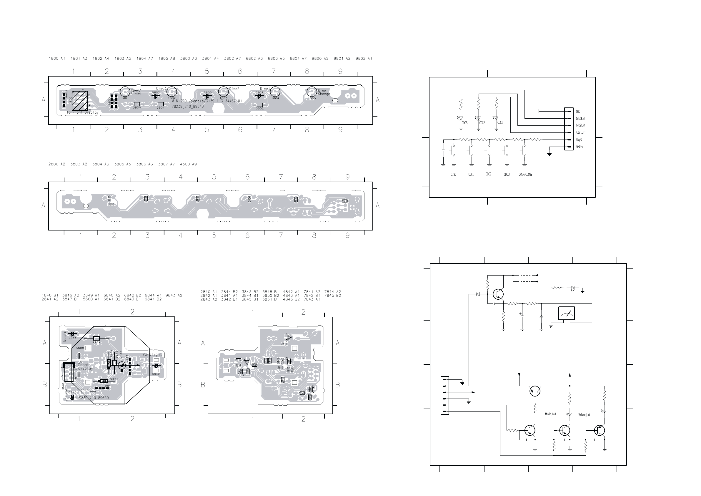
KEY-CDC BOARD - CIRCUIT DIAGRAMKEY-CDC BOARD - COMPONENT LAYOUT
This assembly drawing shows a summary of all possible versions. For components used in a specific version see schematic diagram and respective parts list.
KEY-CDC BOARD - CHIP LAYOUT
3139 113 3446 pt2 dd wk0116
1800 A3
1801 B2
1802 B2
1803 B2
1804 B1
1805 B1
2800 B1
3800 A1
3801 A1
3802 A2
123
Note : Some values may varies, see respective parts list for correct value.
3801
3800
220R
220R
3802
220R
A
6804
3803
560R
1805
6803
1804
3804
390R
3805
270R
1803
3806
220R
1802
2800
6802
100p
B
GND-B GND-B
GND-B GND-B
1
GND-B
GND-B
3139 118 54530...for 89610...3446 pt2 dd wk0116
23
3803 A1
3804 A1
GND
3807
150R
1801
3805 A2
3806 A2
GND-B
3807 A2
6802 A1
FE-ST-VK-N
1800
1
2
3
4
5
6
6803 A1
6804 A2
A
B
This assembly drawing shows a summary of all possible versions. For components used in a specific version see schematic diagram and respective parts list.
VU METER BOARD - COMPONENT LAYOUT VU METER BOARD - CHIP LAYOUT
This assembly drawing shows a summary of all possible versions.
For components used in a specific version see schematic diagram and respective parts list.
3139 113 3446 pt2 dd wk0116
This assembly drawing shows a summary of all possible versions.
For components used in a specific version see schematic diagram and respective parts list.
3139 113 3446 pt2 dd wk0116
3139 113 3446 pt2 dd wk0116
VU METER BOARD - CIRCUIT DIAGRAM
1840 C1
2842 D2
3841 A2
3844 A3
3847 D4
3850 C4
2840 A2
2843 D3
3842 A2
3845 D2
2841 A2
2844 D4
3843 A2
3846 D3
3848 C3
3849 C3
1234
Note : Some values may varies, see respective parts list for correct value.
# : Provision
47K
3841
A
6840
1N4148
2840
100p
3842
7841
BC847B
3843
100K
B
1840
FE-BT-VK-N
1
C
2
3
4
5
6
To Front
D
VUMeter
+5V6
Gnd
Bit0
Bit1
3845
1K2
1K
+5V6
3851 A3
4842 A2
# 4842
4843
2841
2842
100p
3844
8K2
1u
BC857B
Gnd
4843 A2
5600 A4
6840 A1
+5V6
+Vu
6841
7842
3848
470R
7843
BC847B
1N4148
6841 A3
6842 A4
6843 D4
Vu-backlight
3851
180R
12
2843
100p
4K7
Gnd
3846
+Vu
6844
6844 D3
7841 A2
7842 C3
LB3333
6842
3849
150R
7844
BC847B
7843 D3
7844 D3
7845 D4
Gnd
5600
Vu-meter
3847
2844
100p
220R
Gnd
3850
6843
390R
BC857B
7845
A
B
C
D
3139 118 54530...for 89650...3446 pt2 dd wk0116
1234
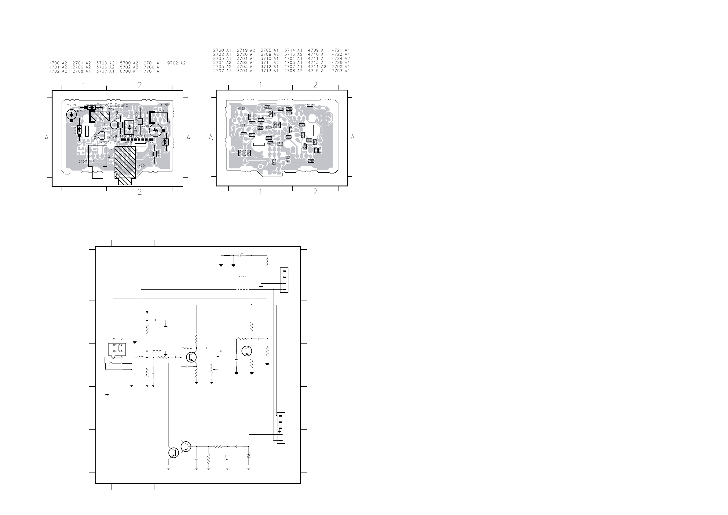
KARAOKE BOARD - COMPONENT LAYOUT KARAOKE BOARD - CHIP LAYOUT
This assembly drawing shows a summary of all possible versions.
For components used in a specific version see schematic diagram and respective parts list.
3139 113 3446 pt2 dd wk0116
KARAOKE BOARD - CIRCUIT DIAGRAM
1700 C1
2700 C1
2703 C3
2706 A3
2719 C3
1701 A4
2701 C2
2702 C2
2704 C3
2705 B4
1702 D4
123 4
Note : Some values may varies, see respective parts list for correct value.
# : Provision
A
2720 B2
2707 E2
3700 B1
2708 E3
SIMPLE KARAOKE
(FOR /21 VERSION ONLY)
3701 C2
3702 C1
3703 C2
3704 C2
3705 B2
3706 C2
This assembly drawing shows a summary of all possible versions.
For components used in a specific version see schematic diagram and respective parts list.
3139 113 3446 pt2 dd wk0116
3707 C3
3711 B4
3714 E3
5700 C1
6701 E4
3709 B4
3710 C4
mic_gnd
3712 C4
3713 A4
agnd
2706
100u
5702
2u2
9702
3715 E3
4708 C3
agnd
5702 A4
6700 E3
3713
470R
7700 C2
7701 C4
1701
FE-BT-VK-N
4
+12A
3
MIC
2
agnd
1
MIC_DET
7702 E2
7703 E2
9702 A4
A
B
3
2
1
C
TC38
1700
agnd
agnd
6
5
4
8
7
9
mic_gnd
D
E
3139 118 54530...for 89630...3446 pt2 dd wk0140
123 4
5700
22u
mic_gnd
3702
+12A
3700
10K
# 2720
100n
1K5
# 3701
330R
2700
mic_gnd
agnd
agnd
3703
10K
4n7
7702
BC847B
agnd
2701
100n
2K7
3705
2703
3704
2702
mic_gnd
BC847B
470n
1M
7700
BC550C
3
1n
7703
3706
2707
agnd
33R
100n
3707
3714
agnd
20K
1
agnd
1M
FOR VIDEO CD ONLY
2719
3715
150K
3711
B
680R
2705
3709
1u
1M
4708
470n
2704
2
6700
1N4148
10u
2708
agnd
agnd
680p
3710
1N4148
agnd
7701
BC550C
330R
agnd
6701
agnd
3712
agnd
100K
FE-BT-VK-N
1
2
3
4
5
1702
C
D
+Kara
VCD_IN1
agnd
VCD_IN2
MIC_DET
E

FRONT DISPLAY BOARD
FRONT DISPLAY BOARD - COMPONENT LAYOUT
This assembly drawing shows a summary of all possible versions. For components used in a specific version see schematic diagram and respective parts list.
3139 113 3447 pt2 dd wk0119
 Loading...