Philips EM8E Service Manual

Colour television Chassis
EM8E
AA
E_14780_000.eps
170704
Contents Page Contents Page
1 Technical Specifications, Connections,
and Chassis Overview 2
2 Safety Instructions, Warnings, and Notes 6
3 Directions for Use 8
4 Mechanical Instructions 9
5 Service Modes, Error Codes, and Faultfinding 15
6 Block Diagrams, Testpoint Overview, and
Waveforms (Not Applicable yet)
Wiring Diagram 32” Sharp LCD 21
7 Circuit Diagrams and PWB layouts Diagram PWB
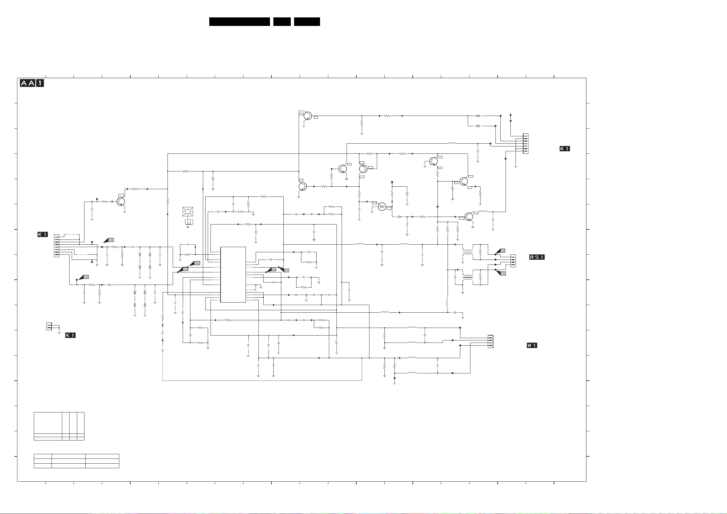
LCoS Audio Amplifier Board (Diagram AA1) 22 23
LCoS System Board (Diagram K1) 24 28
LCoS System Board (Diagram K2) 25 28
LCoS System Board (Diagram K3) 26 28
LCoS System Board (Diagram K4) 27 28
LED Sensor Panel (Diagram LS) 29 30
LCoS Side Jack Panel (Diagram O) 31 32
LCoS LED / Keyboard Panel (Diagram P1) 33 34
LCoS MSB: OSD Insertion (Diagram SL1A) 35 (NA)
LCoS MSB: OSD Insertion (Diagram SL1B) 36 (NA)
LCoS MSB: OSD Insertion (Diagram SL1C) 37 (NA)
LCoS MSB: TMDS-TX (Diagram SL2) 38 (NA)
LCoS MSB: Scaler 1 (Diagram SL3A) 39 (NA)
LCoS MSB: Scaler 2 (Diagram SL3B) 40 (NA)
LCoS MSB: Scaler 3 (Diagram SL3C) 41 (NA)
LCoS MSB: LVDS Receiver (Diagram SL3D) 42 (NA)
LCoS MSB: HD Sync Slicer (Diagram SL4A) 43 (NA)
LCoS MSB: HD2 + VGA Input (Diagram SL4B) 44 (NA)
LCoS MSB: HD1 - 2 Selector (Diagram SL4C) 45 (NA)
LCoS MSB: DVI Receiver (Diagram SL5) 46 (NA)
LCoS MSB: DC-Converter (Diagram SL6) 47 (NA)
Thermo Sensor Panel (Diagram TS1) 48 48
LCoS Main Power Board (Diagram U1) 49 50
LCoS SCART Daughter Board (Diagram VDS1) 51 52
©
Copyright 2004 Philips Consumer Electronics B.V. Eindhoven, The Netherlands.
All rights reserved. No part of this publication may be reproduced, stored in a
retrieval system or transmitted, in any form or by any means, electronic,
mechanical, photocopying, or otherwise without the prior permission of Philips.
LCoS 1fH SCART Panel (Diagram VS1) 53 56
LCoS 1fH SCART Panel (Diagram VS2) 54 56
LCoS 1fH SCART Panel (Diagram VS3) 55 56
LCoS Input Power Board (Diagram W1) 57 59
LCoS Input Power Board (Diagram W2) 58 59
8 Alignments 61
9 Circuit Descriptions 67
List of Abbreviations 93
IC Data Sheets (Not Applicable)
10 Spare Parts List 95
11 Revision List 106
Published by JH 0467 TV Service Printed in The Netherlands Subject to modification EN 3122 785 14780
EN 2 EM8E1.
Technical Specifications, Connections, and Chassis Overview
1. Technical Specifications, Connections, and Chassis Overview
Index of this chapter:
1. Technical Specifications
2. Connections
3. Chassis Overview
Note: Figures below can deviate slightly from the actual
situation, due to the different set executions.
1.1 Technical Specifications
1.1.1 Vision
Display type : Rear projection, LCD
Screen size : 55” (140 cm), 16:9
Resolution (HxV) : 1280 x 720p, WXGA
Viewing angle (HxV) : 160 x 120 deg.
Tuning system : PLL
Colour systems : PAL B/G, D/K, I
: SECAM B/G, D/K, L/L’
Add. systems Ext in : NTSC 3.58, 4.43
: 576i (YPrPb)
: 576p (YPrPb)
: 720p
: 1080i
: SECAM
: VGA (640 x 400)
: VGA (640 x 480)
: WVGA (848 x 480)
: WVGA (852 x 480)
: SVGA (800 x 600)
: XGA (1024 x 768)
: SXGA (1280 x 1024)
Channel selections : 100 presets
: UVSH
Aerial input : 75 ohm, IEC-type
1.1.2 Sound
1.2 Connections
Note: The following connector colour abbreviations are used
(acc. to DIN/IEC 757): Bk= Black, Bu= Blue, Gn= Green, Gy=
Grey, Rd= Red, Wh= White, and Ye= Yellow.
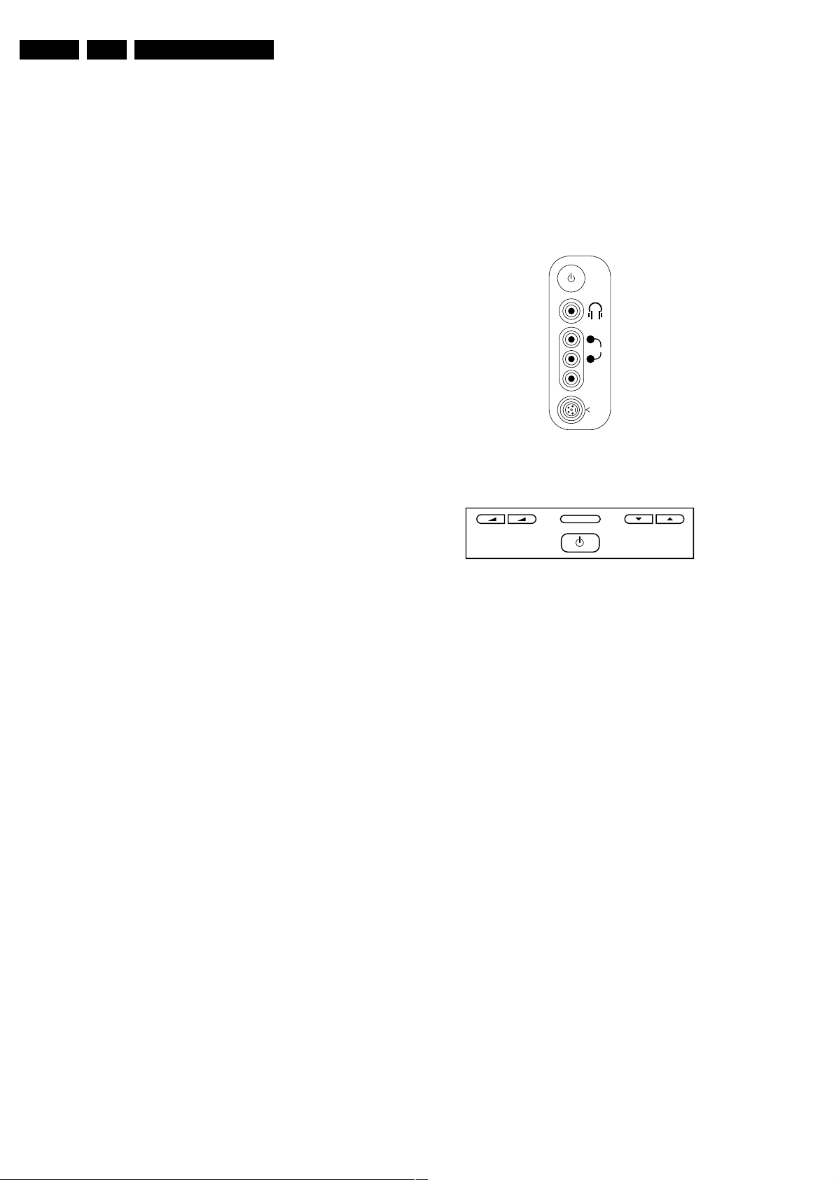
1.2.1 Side Connections / Top Control
R
AUDIO
L
VIDEO
S-VIDEO
E_14780_011.eps
250604
Figure 1-1 Side I/O connections
-+
VOLUME CHANEL
Figure 1-2 Top Control
Mini Jack: Audio Headphone - Out
Bk -Headphone 32 - 600 ohm / 10 mW ot
MENU
E_14780_012.eps
250604
Sound systems : AV stereo,
: FM/FM B/G (5.5-5.74)
: FM/FM Cz (6.5-6.25)
: NICAM B/G (5.5-5.85)
: NICAM D/K (5.5-5.85)
: NICAM I (6.0-6.52)
: NICAM L (6.5AM-
5.85)
Maximum power : 2 x 25 WRMS (int.)
1.1.3 Miscellaneous
Power supply:
- Mains voltage : 220 - 240 VAC
- Mains frequency : 50 / 60 Hz.
Ambient conditions:
- Temperature range : +5 to +40 deg. C
- Maximum humidity : 90 % R.H.
Power consumption
- Normal operation : ca. 270 W
- Standby : < 1 W
Dimensions (WxHxD) : 1437 x 968 x 443 cm
Weight : 40 kg
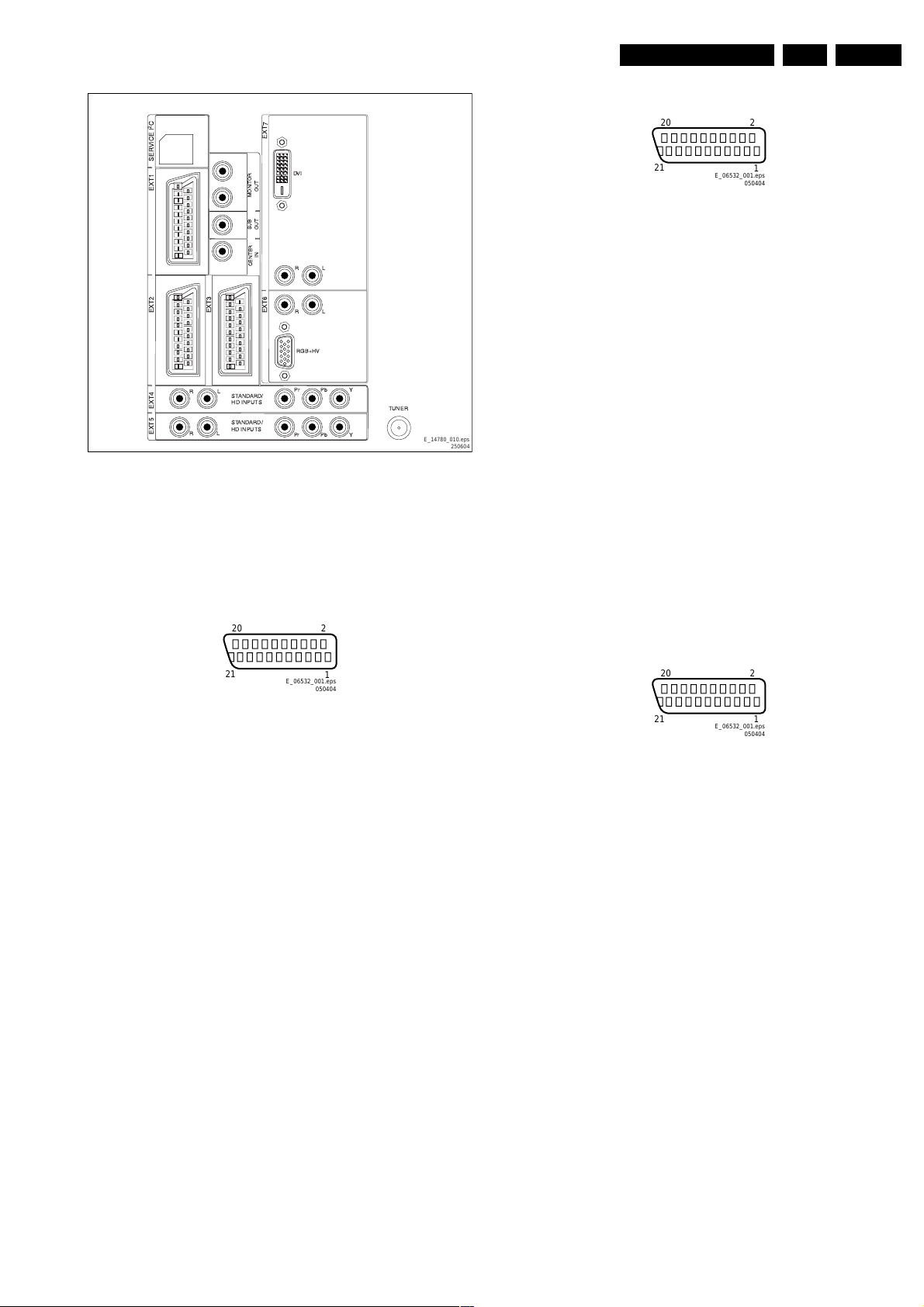
1.2.2 Rear Connections
Cinch: Audio - In, CVBS - In
Re - Audio - R 0.5 VRMS / 10 kohm jq
Wh -Audio - L 0.5 VRMS / 10 kohm jq
Ye -CVBS 1 VPP / 75 ohm jq
Hosiden: SVHS - In
1-Y Ground H
2-C Ground H
3-Y 1 VPP / 75 ohm j
4-C 0.3 VPP / 75 ohm j
Technical Specifications, Connections, and Chassis Overview
External 2: Audio - In/Out, RGB/YUV - In, CVBS - In/Out
EN 3EM8E 1.
C
2
EXT3
R
L
EXT5 EXT4 EXT2 EXT1 SERVICE I
L
R
STANDARD/
HD INPUTS
STANDARD/
HD INPUTS
OUT
MONITOR
SUB
OUT
IN
CENTER
EXT7
EXT6
DVI
R
R
RGB+HV
PrPrPb
L
L
Y
TUNER
Pb
Y
E_14780_010.eps
250604
Figure 1-3 Rear connections
Service Connector (ComPair)
1-SDA-S I2C data (5 V) jk
2-SCL-S I2C clock (5 V) j
3-GND Ground H
External 1: Audio In/Out, RGB/YUV - In , CVBS - In/Out
20
2
20
21
2
E_06532_001.eps
050404
1
Figure 1-5 SCART connector
1-Audio - R 0.5 VRMS / 1 kohm k
2-Audio - R 0.5 VRMS / 10 kohm j
3-Audio - L 0.5 VRMS / 1 kohm k
4-Audio - gnd Ground H
5-Blue - gnd Ground H
6-Audio - L 0.5 VRMS / 10 kohm j
7-Blue/U - in 0.7 VPP / 75 ohm j
8-CVBS-status 0 - 2 V: INT
4.5 - 7 V: EXT 16:9
9.5 - 12 V: EXT 4:3 j
9-Green - gnd Ground H
10 - Easylink P50 j
11 - Green/Y - in 0.7 VPP / 75 ohm j
12 - n.c.
13 - Red - gnd Ground H
14 - FBL - gnd Ground H
15 - Red/V - in 0.7 VPP / 75 ohm j
16 - Status/FBL 0 - 0.4 V: INT
1 - 3 V: EXT / 75 ohm j
17 - Video Ground H
18 - Video Ground H
19 - CVBS - out 1 VPP / 75 ohm k
20 - CVBS - in 1 VPP / 75 ohm j
21 - Shielding Ground H
External 3: Audio - In, CVBS - In
21
E_06532_001.eps
050404
1
Figure 1-4 SCART connector
1-Audio - R 0.5 VRMS / 1 kohm k
2-Audio - R 0.5 VRMS / 10 kohm j
3-Audio - L 0.5 VRMS / 1 kohm k
4-Audio - gnd Ground H
5-Blue - gnd Ground H
6-Audio - L 0.5 VRMS / 10 kohm j
7-Blue/U - in 0.7 VPP / 75 ohm j
8-CVBS-status 0 - 2 V: INT
4.5 - 7 V: EXT 16:9
9.5 - 12 V: EXT 4:3 j
9-Green - gnd Ground H
10 - n.c.
11 - Green/Y - in 0.7 VPP / 75 ohm j
12 - n.c.
13 - Red - gnd Ground H
14 - FBL - gnd Ground H
15 - Red/V - in 0.7 VPP / 75 ohm j
16 - Status/FBL 0 - 0.4 V: INT
1 - 3 V: EXT / 75 ohm j
17 - Video Ground H
18 - Video Ground H
19 - CVBS - out 1 VPP / 75 ohm k
20 - CVBS - in 1 VPP / 75 ohm j
21 - Shielding Ground H
20
21
2
E_06532_001.eps
050404
1
Figure 1-6 SCART connector
1-n.c.
2-Audio - R 0.5 VRMS / 10 kohm j
3-n.c.
4-Audio - gnd Ground H
5-Blue - gnd Ground H
6-Audio - L 0.5 VRMS / 10 kohm j
7-n.c.
8-CVBS-status 0 - 2 V: INT
4.5 - 7 V: EXT 16:9
9.5 - 12 V: EXT 4:3 j
9-Green - gnd Ground H
10 - n.c.
11 - n.c.
12 - n.c.
13 - Red - gnd Ground H
14 - FBL - gnd Ground H
15 - n.c.
16 - n.c.
17 - Video Ground H
18 - Video Ground H
19 - n.c.
20 - CVBS - in 1 VPP / 75 ohm j
21 - Shielding Ground H
EN 4 EM8E1.
Technical Specifications, Connections, and Chassis Overview
Cinch: Audio Centre - In
Gn -Centre 0.5 VRMS / 10 kohm jq
Cinch: Audio Subwoofer - Out
Bk -Subwoofer 0.5 VRMS / 1 kohm kq
Cinch: Audio Monitor - Out
Rd -Audio - R 0.5 VRMS / 1 kohm kq
Wh -Audio - L 0.5 VRMS / 1 kohm kq
External 4 (Cinch): YPbPr - In (2fH)
Gn -Y 0.7 VRMS / 10 kohm kq
Bu -Pb 0.7 VRMS / 10 kohm kq
Rd -Pr 0.7 VRMS / 10 kohm kq
Rd -Audio - R 0.5 VRMS / 10 kohm kq
Wh -Audio - L 0.5 VRMS / 10 kohm kq
External 5 (Cinch): YPbPr - In (2fH)
Gn -Y 0.7 VRMS / 10 kohm kq
Bu -Pb 0.7 VRMS / 10 kohm kq
Rd -Pr 0.7 VRMS / 10 kohm kq
Rd -Audio - R 0.5 VRMS / 10 kohm kq
Wh -Audio - L 0.5 VRMS / 10 kohm kq
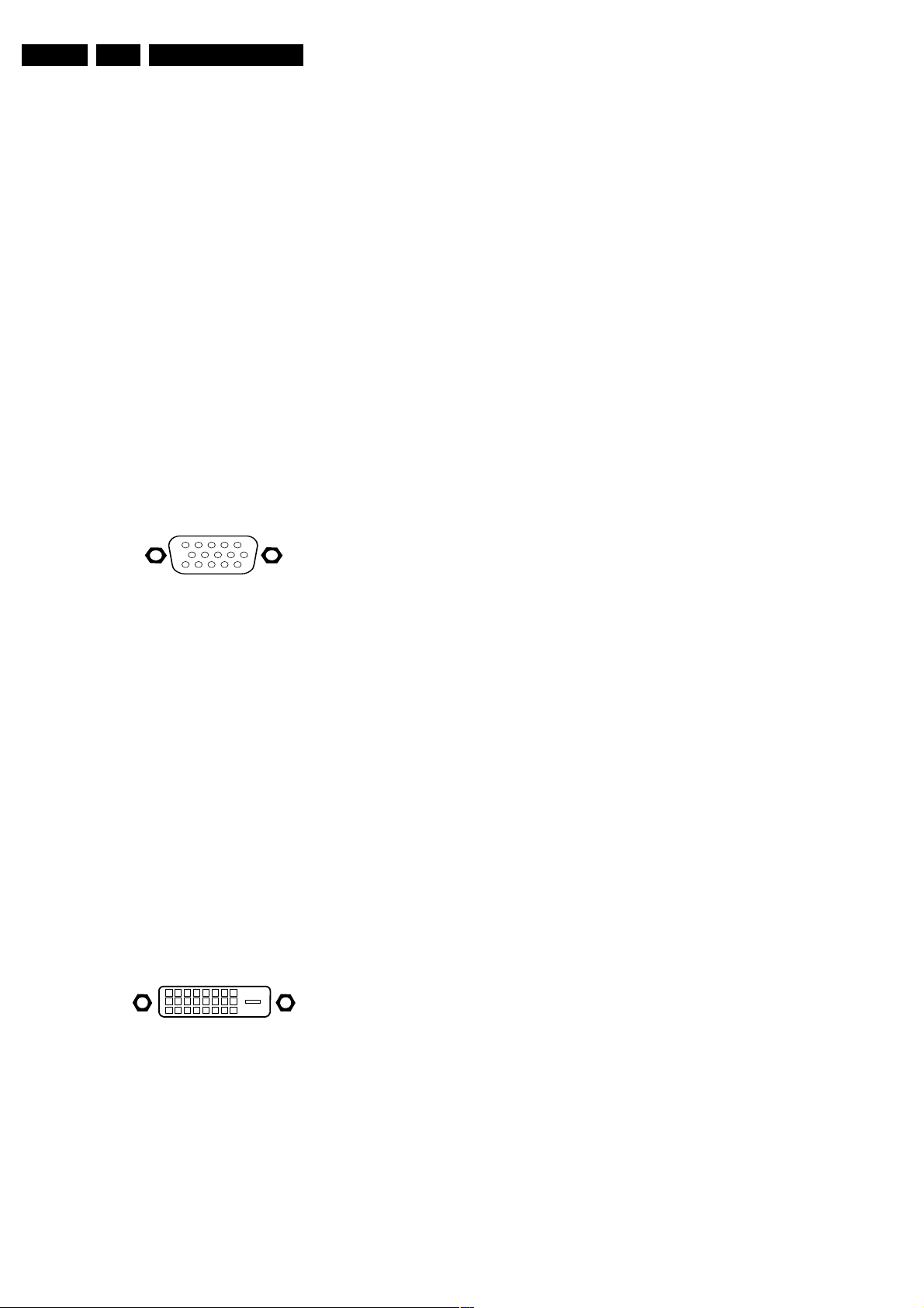
External 6: VGA - In
1
6
11
5
10
15
E_06532_002.eps
050404
11 - Ground GND H
12 - n.c.
13 - n.c.
14 - +5V
15 - Ground GND H
16 - + 5V Hot Plug
17 - RX0- j
18 - RX0+ j
19 - Ground GND H
20 - n.c.
21 - n.c.
22 - Ground GND H
23 - RXC+ j
24 - RXC- j
C5 - Ground GND H
External 7 (Cinch): DVI Audio - In
Rd - Audio - R 0.5 VRMS / 10 kohm jq
Wh -Audio - L 0.5 VRMS / 10 kohm jq
Aerial - In
-IEC-type Coax, 75 ohm D
Figure 1-7 VGA Connector
1-Red 0.7 VPP / 75 ohm j
2-Green 0.7 VPP / 75 ohm j
3-Blue 0.7 VPP / 75 ohm j
4-TXD k
5- Ground H
6-Red Ground H
7-Green Ground H
8-Blue Ground H
9-RC k
10 - Ground H
11 - RXD j
12 - DDC_SDA j
13 - H-sync 0 - 5 V j
14 - V-sync 0 - 5 V j
15 - DDC_SCL j
External 6 (Cinch): VGA Audio - In
Rd -Audio - R 0.5 VRMS / 10 kohm jq
Wh -Audio - L 0.5 VRMS / 10 kohm jq
External 7: DVI-D: In
18
916
17
24
E_06532_003.eps
C5
050404
Figure 1-8 DVI-D connector
1-RX2- j
2-RX2+ j
3-Ground GND H
4- n.c.
5- n.c.
6-SCL_DVI k
7-SDA_DVI jk
8- n.c.
9-RX1- j
10 - RX1+ j
Technical Specifications, Connections, and Chassis Overview
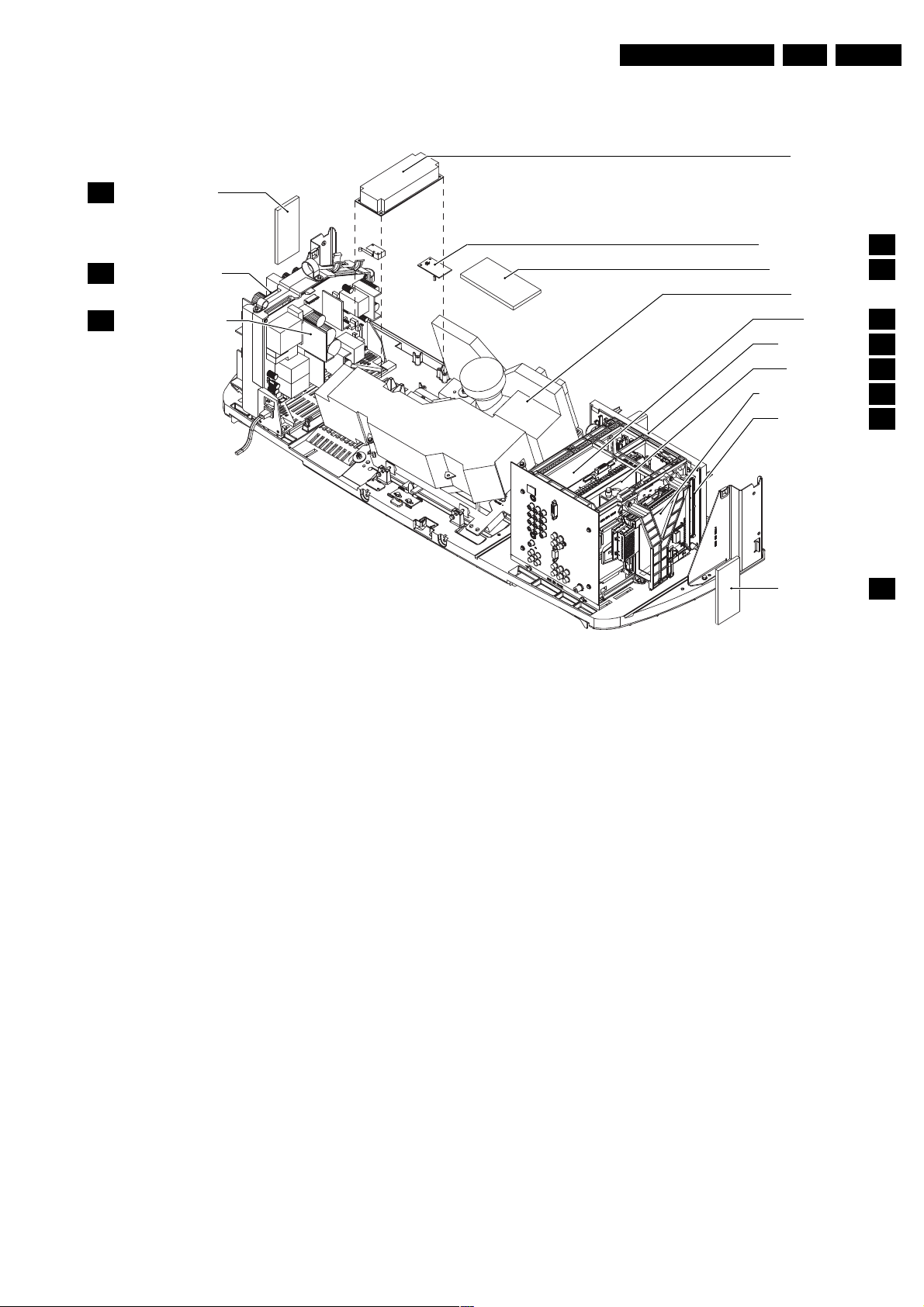
1.3 Chassis Overview
LED SENSOR PANEL
LS
EN 5EM8E 1.
LAMP SUPPLY
MAIN POWER BOARD
U
POWER INPUT BOARD
W
Figure 1-9 PWB location
TEMP SENSOR BOARD
KEYBOARD PANEL
LIGHT ENGINE
JACK PANEL
AUDIO AMPLIFIER
SCALER BOARD
SMALL SIGNAL BOARD
SYSTEM BOARD
SIDE JACK PANEL
E_14780_013.eps
TS
P
VS
AA
SL
B
K
O
190704

EN 6 EM8E2.
Safety Instructions, Warnings, and Notes
2. Safety Instructions, Warnings, and Notes
2.1 Safety Instructions
Safety regulations require that during a repair:
• Connect the set to the mains via an isolation transformer
(> 800 VA).
• Replace safety components, indicated by the symbol h,
only by components identical to the original ones. Any
other component substitution (other than original type) may
increase risk of fire or electrical shock hazard.
Safety regulations require that after a repair, the set must be
returned in its original condition. Pay in particular attention to
the following points:
• Route the wire trees correctly and fix them with the
mounted cable clamps.
• Check the insulation of the mains lead for external
damage.
• Check the strain relief of the mains cord for proper function.
• Check the electrical DC resistance between the mains plug
and the secondary side (only for sets which have a mains
isolated power supply):
1. Unplug the mains cord and connect a wire between the
two pins of the mains plug.
2. Set the mains switch to the "on" position (keep the
mains cord unplugged!).
3. Measure the resistance value between the pins of the
mains plug and the metal shielding of the tuner or the
aerial connection on the set. The reading should be
between 4.5 Mohm and 12 Mohm.
4. Switch "off" the set, and remove the wire between the
two pins of the mains plug.
• Check the cabinet for defects, to avoid touching of any
inner parts by the customer.
2.2 Warnings
voltages in the power supply section both in normal
operation (G) and in standby (F). These values are
indicated by means of the appropriate symbols.
• The semiconductors indicated in the circuit diagram and in
the parts lists, are interchangeable per position with the
semiconductors in the unit, irrespective of the type
indication on these semiconductors.
• Manufactured under license from Dolby Laboratories.
“Dolby”, “Pro Logic” and the “double-D symbol”, are
trademarks of Dolby Laboratories.
E_06532_006.eps
240604
Figure 2-1 Dolby PL Symbol
2.3.2 Schematic Notes
• All resistor values are in ohms and the value multiplier is
often used to indicate the decimal point location (e.g. 2K2
indicates 2.2 kohm).
• Resistor values with no multiplier may be indicated with
either an "E" or an "R" (e.g. 220E or 220R indicates 220
ohm).
• All capacitor values are given in micro-farads (µ= x10-6),
nano-farads (n= x10-9), or pico-farads (p= x10-12).
• Capacitor values may also use the value multiplier as the
decimal point indication (e.g. 2p2 indicates 2.2 pF).
• An "asterisk" (*) indicates component usage varies. Refer
to the diversity tables for the correct values.
• The correct component values are listed in the Electrical
Replacement Parts List. Therefore, always check this list
when there is any doubt.
• All ICs and many other semiconductors are susceptible to
electrostatic discharges (ESD w). Careless handling
during repair can reduce life drastically. Make sure that,
during repair, you are connected with the same potential as
the mass of the set by a wristband with resistance. Keep
components and tools also at this same potential.
Available ESD protection equipment:
– Complete kit ESD3 (small tablemat, wristband,
connection box, extension cable and earth cable) 4822
310 10671.
– Wristband tester 4822 344 13999.
• Be careful during measurements in the high voltage
section.
• Never replace modules or other components while the unit
is switched "on".
• When you align the set, use plastic rather than metal tools.
This will prevent any short circuits and the danger of a
circuit becoming unstable.
2.3 Notes
2.3.1 General
• Measure the voltages and waveforms with regard to the
chassis (= tuner) ground (H), or hot ground (I), depending
on the tested area of circuitry. The voltages and waveforms
shown in the diagrams are indicative. Measure them in the
Service Default Mode (see chapter 5) with a colour bar
signal and stereo sound (L: 3 kHz, R: 1 kHz unless stated
otherwise) and picture carrier at 475.25 MHz for PAL, or
61.25 MHz for NTSC (channel 3).
• Where necessary, measure the waveforms and voltages
with (D) and without (E) aerial signal. Measure the
2.3.3 Rework on BGA (Ball Grid Array) ICs
General
Although (LF)BGA assembly yields are very high, there may
still be a requirement for component rework. By rework, we
mean the process of removing the component from the PWB
and replacing it with a new component. If an (LF)BGA is
removed from a PWB, the solder balls of the component are
deformed drastically so the removed (LF)BGA has to be
discarded.
Device Removal
As is the case with any component that, it is essential when
removing an (LF)BGA, the board, tracks, solder lands, or
surrounding components are not damaged. To remove an
(LF)BGA, the board must be uniformly heated to a temperature
close to the reflow soldering temperature. A uniform
temperature reduces the chance of warping the PWB.
To do this, we recommend that the board is heated until it is
certain that all the joints are molten. Then carefully pull the
component off the board with a vacuum nozzle. For the
appropriate temperature profiles, see the IC data sheet.
Area Preparation
When the component has been removed, the vacant IC area
must be cleaned before replacing the (LF)BGA.
Removing an IC often leaves varying amounts of solder on the
mounting lands. This excessive solder can be removed with
either a solder sucker or solder wick. The remaining flux can be
removed with a brush and cleaning agent.
After the board is properly cleaned and inspected, apply flux on
the solder lands and on the connection balls of the (LF)BGA.
Note: Do not apply solder paste, as this has shown to result in
problems during re-soldering.

Safety Instructions, Warnings, and Notes
Device Replacement
The last step in the repair process is to solder the new
component on the board. Ideally, the (LF)BGA should be
aligned under a microscope or magnifying glass. If this is not
possible, try to align the (LF)BGA with any board markers.
To reflow the solder, apply a temperature profile according to
the IC data sheet. So as not to damage neighbouring
components, it may be necessary to reduce some
temperatures and times.
More Information
For more information on how to handle BGA devices, visit this
URL:
http://www.atyourservice.ce.philips.com (needs
subscription). After login, select “Magazine”, then go to
“Workshop Information”. Here you will find Information on how
to deal with BGA-ICs.
2.3.4 Practical Service Precautions
• It makes sense to avoid exposure to electrical shock.
While some sources are expected to have a possible
dangerous impact, others of quite high potential are of
limited current and are sometimes held in less regard.
• Always respect voltages. While some may not be
dangerous in themselves, they can cause unexpected
reactions - reactions that are best avoided. Before reaching
into a powered TV set, it is best to test the high voltage
insulation. It is easy to do, and is a good service precaution.
EN 7EM8E 2.

EN 8 EM8E3.
3. Directions for Use
You can download this information from the following website:
http://www.philips.com/support
Directions for Use
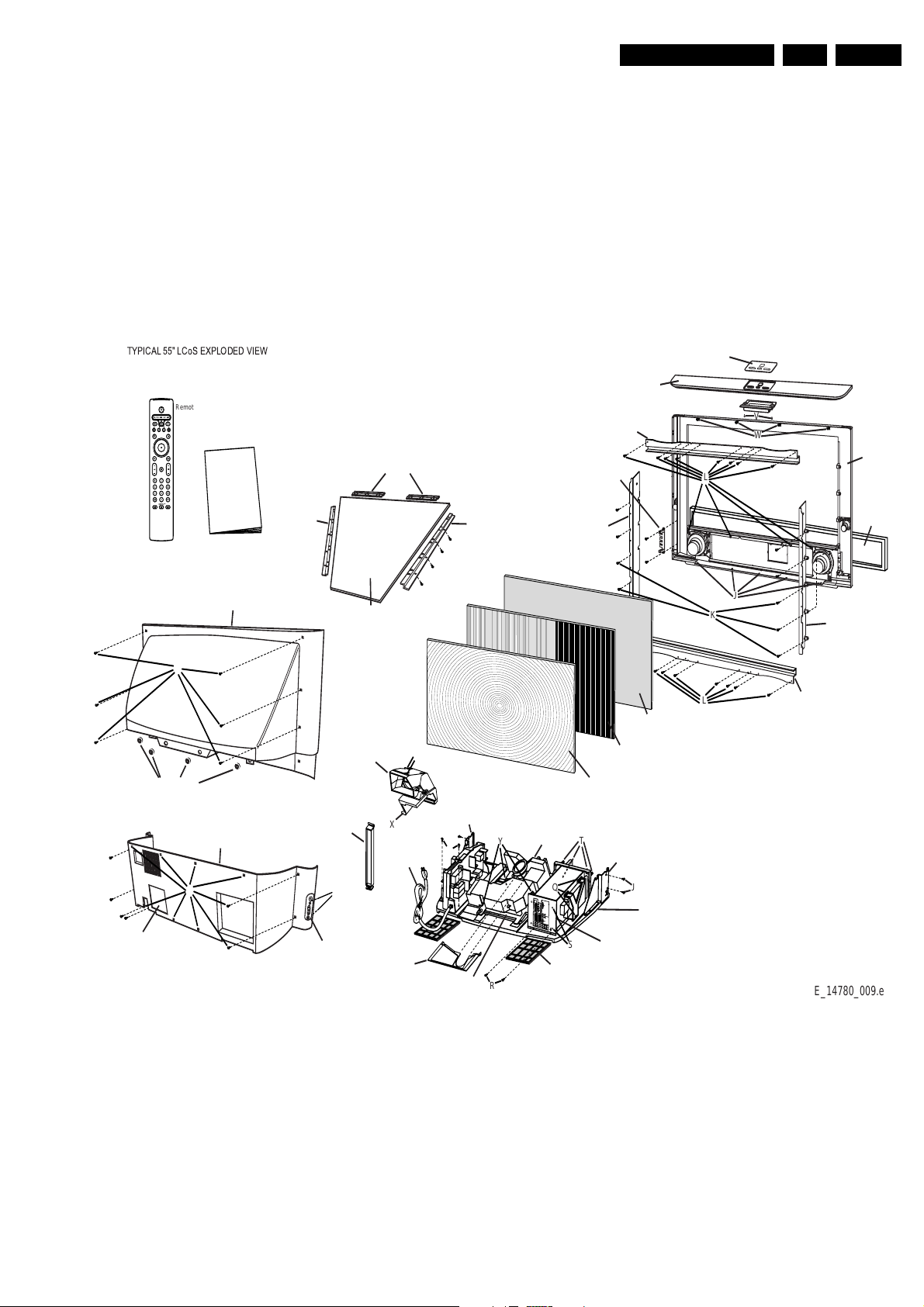
4. Mechanical Instructions
Mechanical Instructions
EN 9EM8E 4.
Index of this chapter:
1. Dust Filter
2. Rear Covers
3. Mirror
4. Top Control
5. Speakers
6. Screen Assembly
7. Side Jack Panel
8. Small Signal Package
9. Large Signal Package
10. LED/Sensor Panel
11. Lamp Replacement
Remote Control
N
¨
¨
¨
¨
DFU
Owner's Manual
Item 0034
Back Cover,
(Upper)
Item 0080
Support,
Mirror,
(Left)
Item 0021
Mirror
Item 0078
Support,
Mirror,
(Top)
Item 0079
Support,
Mirror,
(Right)
12. Light Engine Replacement
13. Re-assembly
Notes:
• Figures below can deviate slightly from the actual situation,
due to the different set executions.
• Follow the disassemble instructions in described order.
• Use Torx T10 and T20 screwdrivers to dismantle the set.
Item 0066
Overlay,
Control Housing
L
J
K
V
W
Item 0076
Rail, Screen,
(Vertical Right)
Item 0030
Front,
Cabinet
Item 0039
Baffle,
Speakers
Rail, Screen,
(Horizontal)
Item 0132
Frame, LED
Sensor Board
Item 0075
Rail, Screen,
(Vertical Left)
Item 0077
Item 0032
Cap,
(Top)
Item 0096
Door,
Lamp Access
C
Item 0144 & 0145
Cap Mounting
A
Item 0036
Back Cover,
(Lower)
Item 0093
Support,
Back
B
Item 0127
Side Jacks for
Mains Knob
Item 0150
Fan Assembly
Item 8190 (UK/HK)
Item 8191 (Europe)
D
Item 0090
Bracket,
X
Mains Cord
Item 0023
Light
Shield
Left Interconnect
N
Item 0018
Bracket,
Light Engine
R
Figure 4-1 Exploded view
Item 0077
L
Item 0022
Screen,
Protector
Item 0019
Screen,
Lenticular
Item 0020
Lens,
Fresnel
Item 0017
Xion-1
Light Engine
Y
Q
Item 0098
Assembly Filter
(2 Required)
T
S
Item 0091
Bracket,
Right Interconnect
Item 0067
Label,
Rear Jack Scart
J
Item 0038
Base,
Cabinet
Rail, Screen,
(Horizontal)
E_14780_009.eps
240604
EN 10 EM8E4.
Mechanical Instructions
4.1 Dust Filter (Item 0098)
E_14780_071.eps
Figure 4-2 Dust filter removal
One dust filter is located under the Power Cord another one
under the Small Signal Package, to prevent dust buildup in the
set.
Under certain conditions, if this filter becomes dirty, the set
could overheat and shut down.
This item can be replaced by the customer.
290604
• It may be necessary to press on the sides of the upper back
where it “snaps” into place at the front cabinet to get it to
release.
• When replacing the Upper Cabinet Rear, care should be
used to properly route the cable for theTop Control
assembly.
• When re-installing the Upper Cabinet Rear, care should be
taken to correctly position the Light Shield that is attached
to the Upper Cabinet Rear.
1. Remove (8) T20 Torx screws (C).
2. Remove (2) T20 Torx screws (D) attaching the Fan Motor
Assembly to the Upper Rear Cover.
3. Remove (4) T20 Torx screws (E) attaching the small signal
cable assembly harness to the Upper Cabinet Rear (not
shown).
4.3 Mirror (Item 0021)
1. Remove both Lower and Upper Rear Covers.
2. Remove both the Left and Right Vertical mirror support
brackets (items 0079 and 0080).
3. Remove both Horizontal Mirror support brackets and
remove the mirror (items 0078).
Note: Care should be taken NOT to place fingerprints or
smudges on the mirror.
4.2 Rear Covers
4.2.1 Lower Rear Cover (item 0036)
1. Make sure all power-, audio-, video-, coax-, and SCART
cables are unplugged.
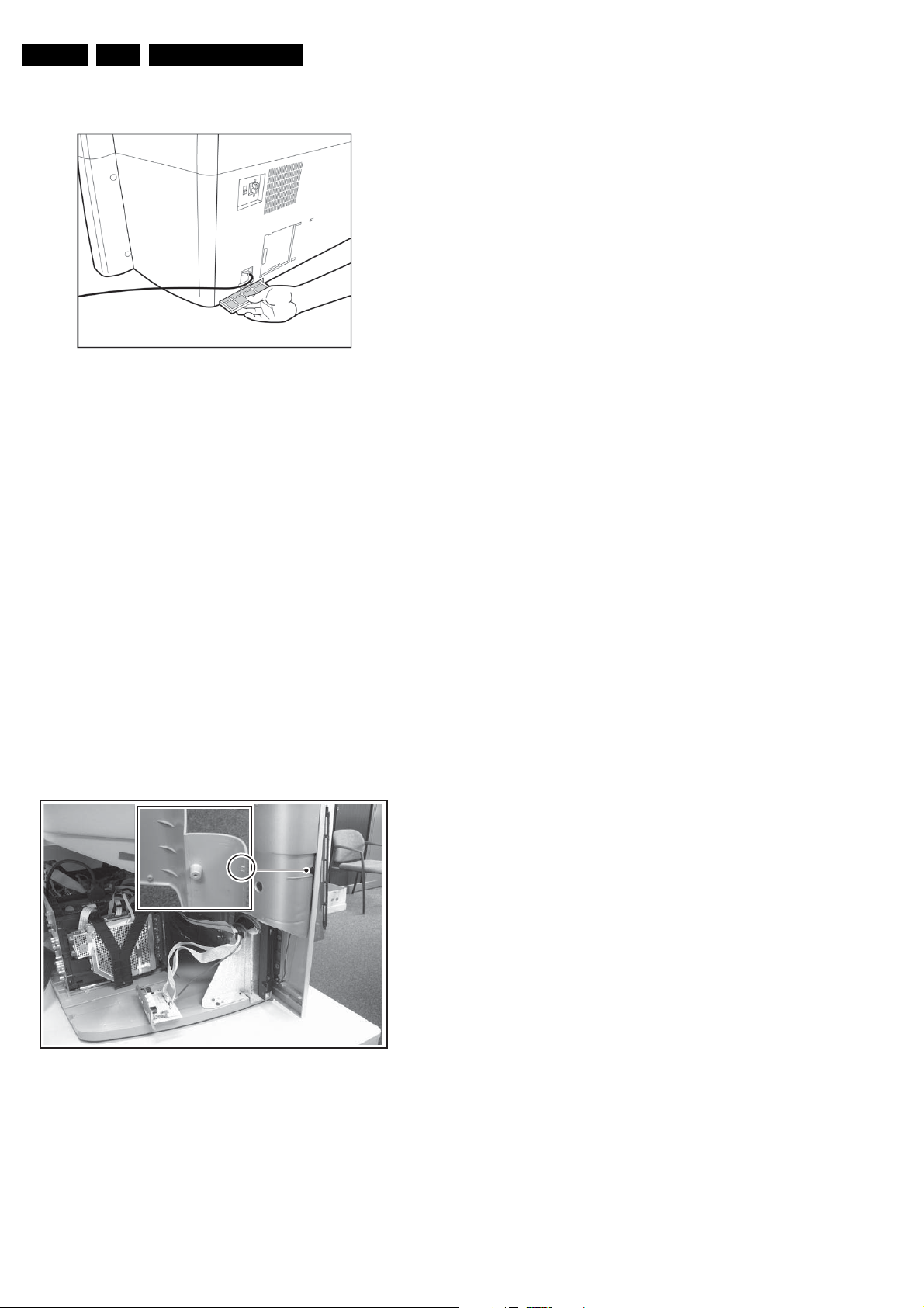
2. Remove all fixation screws (A) from the Rear Cover (lower
part only).
3. Pull the Rear Cover a few inches away from the set. Note:
It is clamped at the upper left and right side. Therefore you
must e.g. insert a thin metal plate (do not use a
screwdriver!) to release this clamp (see figure “Rear cover
clamp”).
4. Now, unplug the Side Jack panel (B).
5. Remove the Rear Cover and set it aside.
4.4 Top Control (Item 1032)
1. Remove (2) T20 Torx screws (V) holding the Keyboard and
cover to the cabinet cap.
2. Remove (2) T6 Torx screws holding the circuit board to the
control bracket.
3. Release (4) plastic clips holding the circuit board to the
control bracket and lift the PWB from the bracket.
4. Disconnect connector 1201 and ground clip 1202.
4.5 Speakers
4.5.1 Woofer (Item 5213)
1. Remove Lower Rear Cover item 0034.
2. Remove (2) T20 Torx screws (R) to allow the small signal
assembly to slide to the rear.
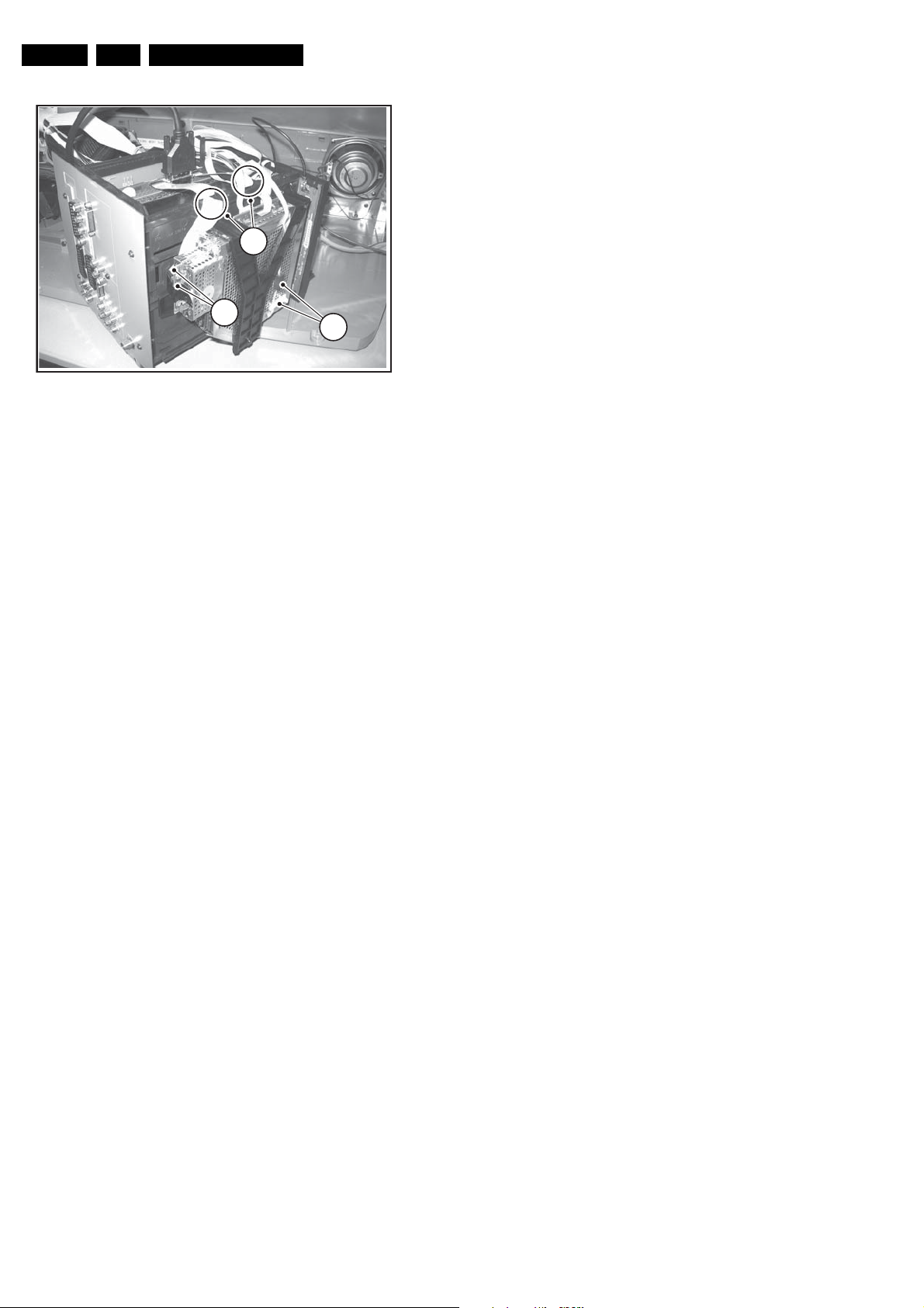
3. Remove (2) T20 Torx screws (N) to allow the power
assembly to slide to the rear.
4. Remove (4) T20 Torx screws from the speakers and
disconnect the speaker wires.
4.5.2 Tweeter (Item 5214)
1. Remove both the Lower and Upper Rear Covers.
2. Remove (2) T20 Torx screws and disconnect the speaker
wires.
Figure 4-3 Rear cover clamp
4.2.2 Upper Rear Cover (Item 0034)
Notes:
• The Lower Rear Cover must be removed before removing
the Upper Rear Cover.
• The Upper Rear Cover holds the Mirror.
E_14780_001.eps
240604
4.5.3 Speaker Baffle (Item 0039)
Note: There are no adjustments that require the removal of the
speaker baffle.
Caution: Do NOT reposition the light engine to gain access to
the speaker baffle tabs.
1. Remove the Lower Rear Cover.
2. Carefully release the (20) plastic tabs holding the speaker
baffle in place.
Mechanical Instructions
EN 11EM8E 4.
4.6 Screen Assembly (Item 0030)
1. Remove the Lower and Upper Rear Covers.
2. Remove (4) T20 Torx screws (W) and remove the Top Cap
with Customer Control Assembly (0032).
3. Disconnect the Tweeter speaker wiring.
4. Remove (9) T20 Torx screws (J).
5. Lay lens assembly on flat clean surface.
6. Remove (12) T20 Torx screws (K) from vertical side rails
Item 0075 and 0076.
7. Remove (16) T20 Torx screws (L) from horizontal screen
rails Item 0077.
4.7 Side Jack Panel (Item 0127)
• Make sure all cables of the Side Jack panel are unplugged.
• Remove the two mounting screws.
• Unlock the clamps, which secure the panel, and remove
the Side Jack panel.
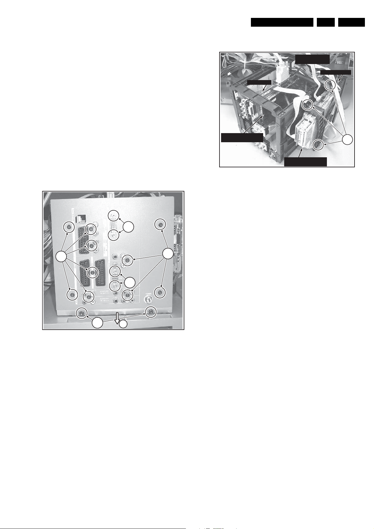
4.8 Small Signal Package
3
4.8.2 Jack Panel
AUDIO AMPLIFIER
(at the rear)
SYSTEM BOARD
JACK PANEL
MAIN SCALER BOARD
(MSB)
SMALL SIGNAL BOARD
(SSB)
Figure 4-5 Boards of the Small Signal Package
Pull out the Jack panel from the Small Signal Package,
unplugging it from the System Board connector.
See Figure “Boards of the Small Signal Package”.
Note: For measurements it is sometimes necessary to place
the Jack Panel in a service position. In this case it is necessary
to use the specific “Extending card” (4835 310 57605)
1
E_14780_002.eps
240604
2
3
1a
1b
Figure 4-4 Small Signal Package
1. Remove the two package mounting screws (1a).
1. Slide the Small Signal Package forward (1b).
4.8.1 Cover Plate
1. Remove all Cover Plate mounting screws (2). See Figure
“Small Signal Package”.
2. Use a 5 mm socket screwdriver to remove the four
connector distance bolts (3). See Figure “Small Signal
Package”.
3. Remove the Cover Plate.
2
E_14780_005.eps
240604
4.8.3 Main Scaler Board (MSB)
1. Disconnect the DVI connector and all cables from the top
of the MSB.
2. Pull out the MSB from the Small Signal package,
unplugging it from the System Board connector.
3. Remove both cover shields from the MSB.
See Figure “Boards of the Small Signal Package”.
Note: For measurements it is sometimes necessary to place
the MSB in a service position. In this case it is necessary to use
the specific “Extending card”, including two cables (4835 310
57605).
4.8.4 Small Signal Board (SSB)
1. Disconnect all cables from the SSB.
2. Remove the three mounting screws (1) from the SSB
bracket. See Figure “Boards of the Small Signal package”.
3. Carefully pull out the SSB, unplugging it from the System
Board connector.
4. Remove all shieldings from the SSB.
Note: For measurements sometimes it is necessary to place
the SSB in a service position. In this case it is necessary to use
the specific “Repair kit board” (order nr. 9965 000 14526)
4.8.5 Audio Amplifier Board
The Audio Amplifier is located at the rear of the System Board.
1. Disconnect all cables from the Audio Amplifier board.
2. Remove the four mounting board screws.
3. Remove the board.
EN 12 EM8E4.
Mechanical Instructions
4.8.6 System Board
Figure 4-6 Rear side of the Small Signal Package
4.9.1 Main Power Board
1. Remove the six board mounting screws (1).
2. Disconnect all cables from the Main Power board.
3. Unlock the clamp, which secures the board at the topside,
and remove the Main Power board.
4.9.2 Input Power Board
1
1. Remove the six board mounting screws.
2. Disconnect all cables from the Input Power Board.
3. Unlock the clamps, which secure the board at the topside,
and remove the Input Power Board.
4.10 LED/Sensor Panel (Item 0132)
E_14780_003.eps
240604
1. Remove the two Sensor panel mounting screws.
2. Remove the Sensor panel bracket.
3. Disconnect all cables from the Sensor panel. Unlock the
two clamps, which secure the panel, and remove the
Sensor panel.
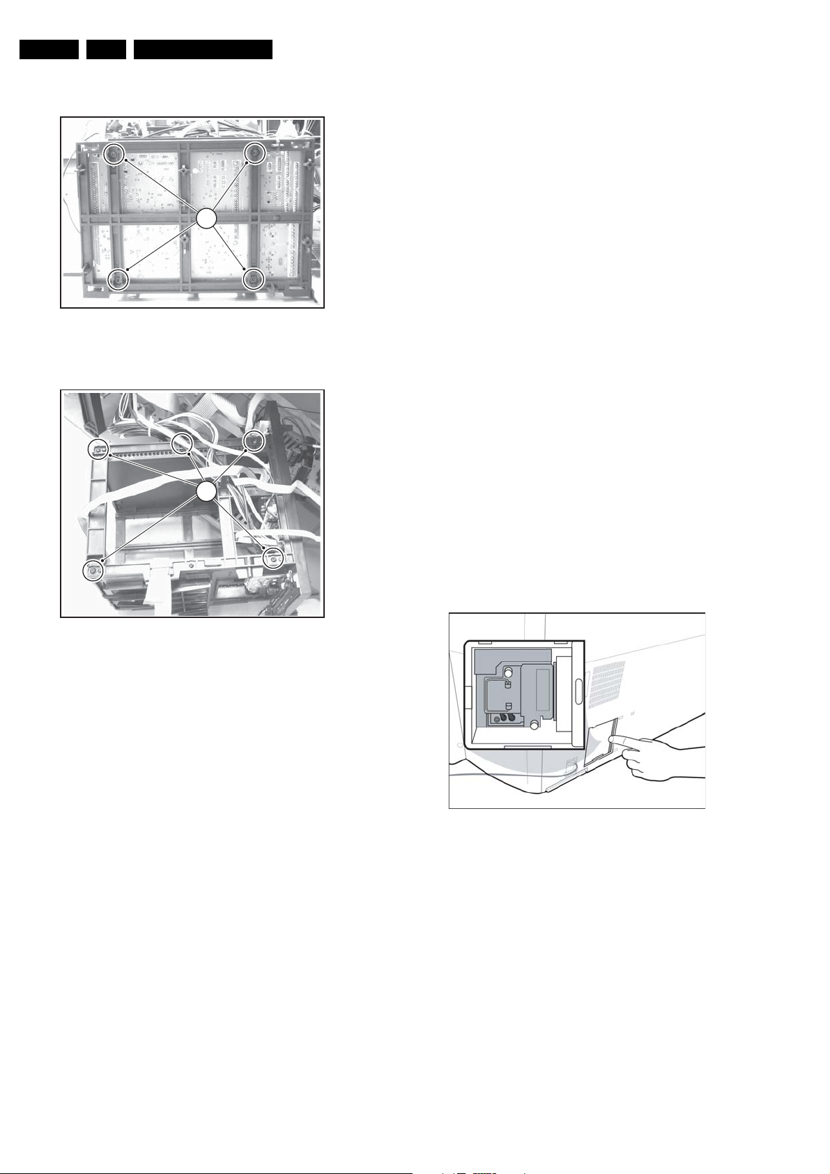
4.11 Lamp Replacement
Caution: The light source lamp produces extreme heat. Allow
a cool-down period before touching or replacing the lamp
1
assembly.
Notes:
• The lamp is easy accesible via the sliding door in the lower
rear cover.
• For protection, the lamp circuit contains a “normally closed”
switch. Therefore, the lamp will not operate with the lamp
access door in the open position.
• There are no tools required for this procedure.
E_14780_004.eps
Figure 4-7 Top side of the Small Signal Package
Note: The Audio, Jack, Scaler, and SSB panels should be
removed prior to removal of the system board.
1. Disconnect all cables from the System Board.
2. Disconnect the Arial-In cable.
3. Remove the four mounting screws at the rear side of the
Small Signal package (1). See Figure “Rear side of the
Small SignalPpackage”.
4. Remove the six mounting screws at the top side of the
Small Signal package (1). See Figure “Top side of the
Small Signal Package”.
5. Remove the six mounting screws from the bottom side of
the Small Signal Package (1). See Figure “Top side of the
Small Signal Package”.
6. Remove the two side panels from the Small Signal
Package.
7. Unlock the clamp, which secures the board at the bottom
side, and remove the System Board.
4.9 Large Signal Package
1. Remove the two Large Signal Package mounting screws
(1). See figure “Cable dressing part 1: PSU” further on.
2. Slide the package out of the set (2). Note: It may be
necessary to release some of the cable holders first.
240604
E_14780_072.eps
290604
Figure 4-8 Lamp replacement
To replace the lamp assembly:
1. Slide the Lamp Access Door on the rear of the unit to the
right.
2. Unscrew the two silver thumbscrews holding the assembly
in place.
3. Slide the old lamp assembly out by crisping the “metal
handle” and pulling straight out.
4. Install the replacement lamp assembly by pushing into
place and tightening the thumbscrews.
5. Slide the Lamp Access Door to the left to close (the unit will
not operate with this door open).
Mechanical Instructions
EN 13EM8E 4.
4.12 Light Engine Replacement
Notes:
• The LCoS Light Engine comes pre-adjusted. No
adjustment for focus should be required. In rare cases, the
set may require a minor focus touch up (see chapter
“Alignments”).
• Due to screw placement, to replace the Light Engine, it is
necessary to remove the upper rear cover before
beginning the replacement. Use care with the routing of the
wiring for the Customer Keypad when replacing the upperback. Also, note mounting direction of the Upper-back
support bracket for proper re-installation.
Caution:
• Do not remove the three “silver” nuts and washers, as
these hold the Light Engine support bracket and are
critical adjustment points for focus and picture alignment.
• The Light Engine has an operating voltage of
approximately 1,000 volts. Always use caution when
working in the vicinity of the Light Engine while the unit is
in operation.
4.13 Re-assembly
To re-assemble the whole set, execute all processes in reverse
order.
Note: While re-assembling the set, make sure that:
• All cables are placed and connected in their original
position (see next figures).
• All cables are routed such that contact with any PWB is
prevented.
• All cables are dressed away from the Lamp Power Supply
(located behind the lamp assy).
• All "grounding" wires are re-connected (Side I/O, Audio
Amplifier, System Board, and PSU).
4.13.1 Cable Dressing
3
4
Remove the screws shown.
1 2
Remove the bracing bar
Figure 4-9 Light engine removal (part 1)
4 4 4
Figure 4-10 Light engine removal (part 2)
E_14780_081.eps
050704
E_14780_082.eps
050704
2
1
E_14780_006.eps
240604
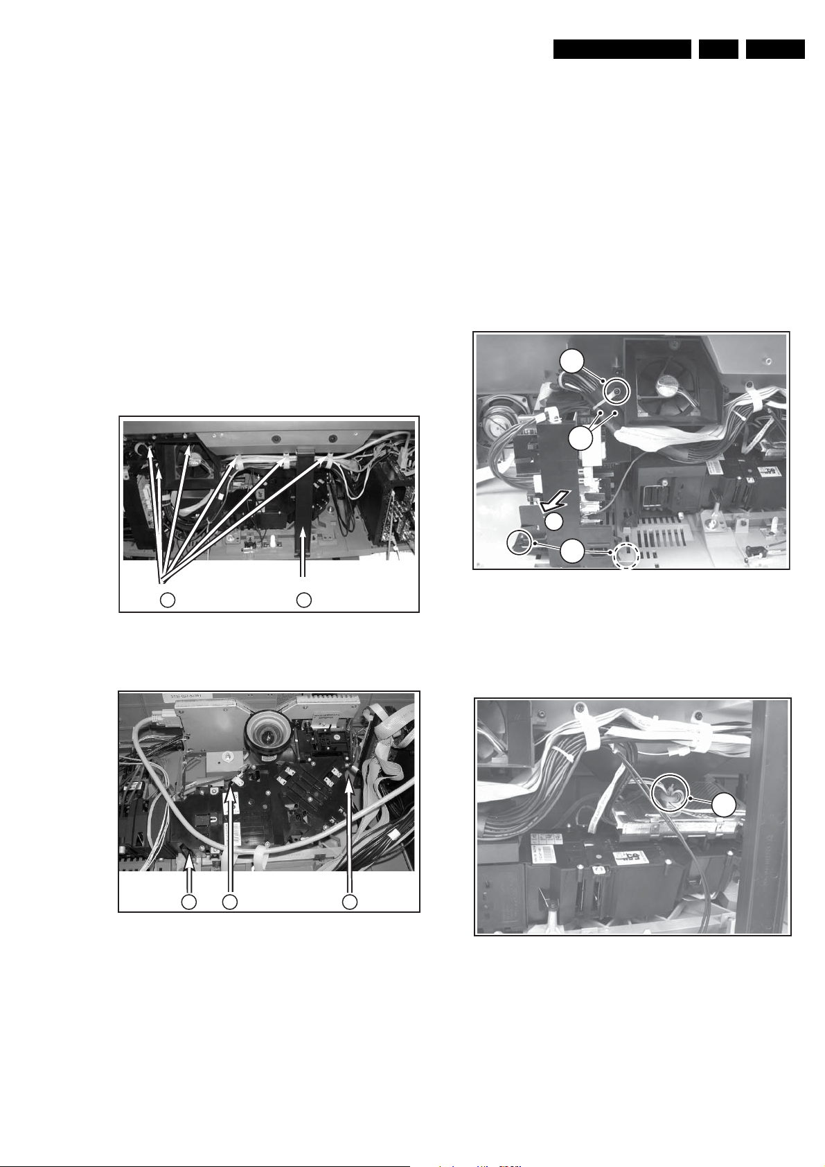
Figure 4-11 Cable dressing part 1: PSU
• Screw mounted cable tie to the fan assy (3).
• Be sure that the wires between the fan assy and the PSU
(4) are fitted with double insulation (heat shrink sleeve).
5
E_14780_007.eps
240604
1. First, disassemble the fan assy and the cable tree (1).
2. Then, remove the bracing bar (2).
3. Next, take out the screws (“C”, see exploded view) and
remove the top cover
4. Remove the three “black” T-10 Torx screws (3) located in
the vicinity of each of the three “silver” nuts and washers.
5. Re-install the Light Engine in reverse order
Figure 4-12 Cable dressing part 2: Light Engine
• Attach the ferrite to the shield (5) with a cable tie .
EN 14 EM8E4.
Mechanical Instructions
8
7
6
E_14780_008.eps
240604
Figure 4-13 Cable dressing part 3: SSP
• Route the flat foil cable through the clip and through the
ferrite (6).
• Be sure that a ferrite (2422 549 00125) is mounted on the
flat foil cable near the PWB connector (7). The flat foil cable
must be secured with tape at this side (the tape must
overlap both sides of the SSB shielding).
• Both flat foil cables from the SSB to the Scaler board must
be routed through the strain reliefs (8) on the bracket.

Service Modes, Error Codes, and Fault Finding
5. Service Modes, Error Codes, and Fault Finding
EN 15EM8E 5.
Index of this chapter
1. Test Conditions
2. Service Modes
3. Error Codes
4. ComPair
5. The “Blinking LED” Procedure
6. Fault Finding
5.1 Test Conditions
The chassis is equipped with test points, printed on the circuit
board assemblies. They refer to the diagram letters. The
numbering is in a logical sequence for diagnostics. Always start
diagnosing (within a functional block), in the sequence of the
relevant test points for that block.
Perform measurements under the following conditions:
• Service Default Mode (SDM).
• Video: colour bar signal.
• Audio: 3 kHz left, 1 kHz right.
5.2 Service Modes
Service Default Mode (SDM) and Service Alignment Mode
(SAM) offer several features for the service technician, while
the Customer Service Mode (CSM) is used for communication
between a Philips Customer Care Centre (P3C) and a
customer.
There is also the option of using ComPair, a hardware interface
between a computer (see requirements below) and the TV
chassis. It offers the ability of structured troubleshooting, test
pattern generation, error code reading, software version
readout, and software upgrading.
Minimum requirements: a Pentium processor, Windows 95/
98, and a CD-ROM drive.
5.2.1 Service Default Mode (SDM)
Upon entry into the Service default mode, the letters “SDM” will
be displayed at the upper right corner of the screen.
Special SDM functions
Access to Normal user menu
Press the “MENU” button on the remote control to switch from
the SDM to the normal user menu (with the SDM mode still
active in the background).
How to exit
To exit the Service default mode, enter zero “0” twice.
Note: To save the error codes, “unplug” the AC power cord
without turning the set "off".
5.2.2 Service Alignment Mode (SAM)
Purpose
The Service alignment mode (SAM) is used to align the set
and/or adjust the option settings and to display/clear the error
code buffer values.
How to activate SAM
Use one of the following methods:
• Via a standard RC transmitter: key in the code “062596”
directly followed by the “OSD [i+]” button. After activating
SAM with this method a service warning will appear on the
screen, you can continue by pressing any digit key on the
RC.
• Short for a moment the two solder pads on the SSP with
the indication "SAM". Depending on the software version,
it is possible that a service warning will appear. You can
continue by pressing any digit key on the RC.
• Use the DST-emulation feature of ComPair.
• Press the ALIGN button on the DST while the set is in the
normal operation
After activating this mode, “SAM” will appear in the upper right
corner of the screen.
Introduction
The Service default mode (SDM) is a technical aid for the
service technician. The Service default mode (SDM)
establishes fixed, repeatable settings of customer controls,
which allow consistent measurements to be made. The SDM
also initiates the blinking LED procedure and, if necessary,
overrides the 5V protection.
The following functions are turned OFF while in SDM:
• Timer
• Sleep timer
The following functions are disabled during SDM (and enabled
after leaving SDM):
• Parental lock
• Blue mute
• Hospitality mode
• No-ident timer (normally the set is automatically switched
off when no video signal (IDENT) is received for 15
minutes).
All other controls operate normally.
How to enter
To enter the Service alignment mode (SAM), press the
following key sequence on the standard remote control
transmitter: 0-6-2-5-9-6-[MENU]. Do not allow the display to
“time out” while entering the key sequence.
• DEFECTIVE MODULE: Displays “Unknown” if no defective module is found.
Contents of SAM
• OPERATION HOURS (Run Timer). Displays the
accumulated total of operational hours (in hexadecimal
format).
• SW VERSION INFO (example):
– ROM VERSION. Displays the date of the software and
the software version of the ROM
(e.g.: EM8EU1_1.0_01234 = AAABBC_X.Y_NNNNN).
• AAA= the chassis name.
• BB= the region: EU= Europe, AP= Asia Pacific
PAL/Multi, AN= Asia Pacific NTSC, US= USA, LT=
LATAM.
• C= the language cluster number.
• X.Y= the software version, where X is the main
version number (different numbers are not
compatible with one another) and Y is the sub
version number (a higher number is always
compatible with a lower number).
• NNNNN= last five digits of 12nc code software.
– SW VERSION MAIN SCALER: Displays the software
version of the MSP.
– SW VERSION EPLD. Displays the software version of
the EPLD.
– SW VERSION GDE: Displays the software version of
the System Board.
• ERRORS (10 errors possible): Displays the 10 most
recent errors. The most recent error is displayed at the
upper left.

EN 16 EM8E5.
Service Modes, Error Codes, and Fault Finding
• RESET ERROR BUFFER: Pressing the “OK” or RIGHT
cursor clears the error buffer and the “Errors” level shows
“No Errors.”
• ALIGNMENTS: Allows access to 6 alignment menus.
General, Luminance Delay, MSB, GDE-Video, GDE-NVM,
and Gamma.
• DEALER OPTIONS: Allows access to dealer “Personal
Options” menu.
• SERVICE OPTIONS: Allows access to 6 service option
menus. Dual Screen, Video repro, Source Select, Audio
repro, Miscellaneous, Opt. No.
• INITIALISE NVM: Not Accessible (only after replacing the
NVM).
• STORE OPTIONS: Select “OK” to save previously
changed selections.
• FUNCTIONAL TEST: Finds module Errors and places the
Error code in the “Errors” register and shows the module
name at the “Defective Module” level. If this test finds no
faults, the ERROR buffer is set to “No Errors” and the
“Defective Module” level shows “NONE.”
• BROADCAST INFO. The purpose of this menu is to debug
the broadcast, NOT the TV. The menu gives an overview
of what is received on the current preset related to Time
extraction, CNI codes, and NexTView transmission.
Following items are displayed:
– Preset. Shows the preset number.
– Local. Local date and time from the selected preset.
– UTC (Coordinated Universal Time). Extracted from the
selected preset.
– LTO (Local Time Offset). Extracted from the selected
preset.
– CNI (Country and Network Identification). Extracted
from the current preset (displayed as a four digit
hexadecimal number. The CNI number identifies the
broadcaster.
– NexTView service (optional). This item gives
information about the type of NexTView service that is
available for the current preset. The possible strings
are:
1. NexTView provider.
2. NexTView data available from preset xx (where xx
is the preset number).
3. No NexTView data available.
– CNI Linking (optional). 'Link' refers to the connection
between the broadcasted NexTView programme
information and the preset number. The possible
strings are:
1. Data available for preset xx xx xx (where xx xx xx
is a list off all presets for which a CNI link is
available).
2. 'Automatic link' or ' Manual link', depending on
what is read from the broadcast and from the CNI
table in the NVM. 'Automatic' means that the link
has been made based on broadcasted information,
without user-interaction. 'Manual' means that the
user has established this link by selecting a preset
in the pop-up menu that you get after setting a
reminder/recording/lock/watch in EPG. Erase a
wrong 'Manual link' by entering the Manual
Installation menu and (without changing anything)
activate 'Store'.
3. Nothing is shown.
How to navigate
• Use the Cursor UP/DOWN keys to select Menu items. The
selected option will be highlighted. When not all menu
options fit on the screen, press the Cursor UP/DOWN or
LEFT/RIGHT keys on the remote transmitter, to display the
next/previous menu.
• With the cursor LEFT/RIGHT keys, it is possible to:
– activate/deactivate the selected menu (e.g.
ALIGNMENTS/GENERAL)
– change the value of the selected menu item (e.g.
TUNER AGC)
– activate the selected submenu (e.g. TEST PATTERN)
How to exit
Press the “MENU” button, enter zero “0” twice, or switch the set
off with the power button.
Note: To save the error codes, “unplug” the AC power cord
without turning the set off.
5.2.3 Customer Service Mode (CSM)
Purpose
When a customer is having problems with his TV-set, he can
call his dealer. The service technician can than ask the
customer to activate the CSM, in order to identify the status of
the set. Now, the service technician can judge the severity of
the complaint. In many cases, he can advise the customer how
to solve the problem, or he can decide if it is necessary to visit
the customer.
The CSM is a read only mode; therefore, modifications in this
mode are not possible.
How to activate CSM
Use one of the following methods:
• Press the “MUTE” button on the RC-transmitter
simultaneously with the “MENU” button on the TV (top
control) for at least 4 seconds.
• Key in the code “123654” via the standard RC transmitter.
Note: Activation of the CSM is only possible if there is no (user)
menu on the screen!
How to navigate
By means of the “CURSOR-DOWN/UP” knob on the RCtransmitter, you can navigate through the menus.
Contents of CSM
CUSTOMER SERVICE MENU 1
• SW VERSION. Displays the built-in software version of the
SSB micrprocessor. In case of field problems related to
software, software can be upgraded. You will find details of
the software versions in the chapter “Software Survey” of
the “Product Survey - Colour Television” publication. This
publication is generated four times a year.
• SW VERSION MAIN. Displays the built-in software
version for the Main Scaler Board.
• SW VERSION EPLD. SW VERSION MAIN. Displays the
built-in software version of the EPLD.
• SW VERSION GDE. SW VERSION MAIN. Displays the
built-in software version of the System Board.
• LIGHT ENG SW VERSION.SW VERSION MAIN.
Displays the built-in software version of the LE.
• LIGHT ENG HW VERSION. Displays the hardware
version of the LE.
• MANUFACTURER’S ID. Each Manufacturer that uses this
Light Engine got an ID number assigned to them. This
number shown in CSM is used to verify that a light engine
for one mfgr did not get mixed up with another mfgr. Size is
up to 5 characters
• PRODUCT ID. This is the product ID, basically the
identification number for the given manufacturer, which
light engine product is hooked up. It will tell if the engine is
a Xion engine, or a Venus engine. For 2k4 based LCoS
products, this means it will always see a XIon ID. For 2k5
with Jaguar, this may be Xion or Venus. Size is up to 5
characters.
• ENGINE DRB SERIAL. The serial number of the DRive
module Board, the electronics of the light engine. Size is up
to 10 characters.
• ENGINE OPTICS SERIAL. This is the serial number of the
optics assemly of the light engine. The big black plastic part
containing the prisms, mirrors, etc. Size is up to 10
characters

Service Modes, Error Codes, and Fault Finding
EN 17EM8E 5.
CUSTOMER SERVICE MENU 2
• LAMP LIFETIME COUNTER. This is the count of hours
since the time the lamp lifetime reset was pressed. This
reset is available to the customer. Range is 0 to 32,767.
• LAMP EXPECTED. This is the setting the customer chose
as the type of lamp he is using, and then the number of
hours based on that type of lamp. (e.g. customer selects
lamp type X, and this is converted into hours) . Range is 0
to 32,767.
• ENGINE LIFETIME. This is the total number of hours the
engine itself has been run with the lamp “on”. This is
important for later service as the Light Engine can be
swapped from final TV to TV. Range is 0 to 32,767.
• POLARIZE LIFETIME. This is the total number of hours
that the polarizer within this light engine has been active.
Again, important because engines can be swapped, or
polarizers repaired and replaced in an existing engine.
Range is 0 to 32,767.
• PANEL LIFETIME. This is the total number of hours that
the LCoS Panel itself within this light engine has been
active. Again, important because engines can be swapped,
or panels repaired and replaced in an existing engine.
Range is 0 to 32,767.
• SET TYPE. This information is very helpful for a help desk/
workshop as reference for further diagnosis. In this way, it
is not necessary for the customer to look at the rear of the
TV-set.
• CODE 1. Gives the latest five errors of the error buffer. As
soon as the built-in diagnose software has detected an
error the buffer is adapted. The last occurred error is
displayed on the left most position. Each error code is
displayed as a 3-digit number. When less than 10 errors
occur, the rest of the buffer is empty (000). See also
paragraph Error Codes for a description.
• CODE 2. Gives the first five errors of the error buffer. See
also paragraph Error Codes for a description.
• VOLUME. Gives the last status of the volume as set by the
customer. The value can vary from 0 (volume is minimum)
to 100 (volume is maximum). Volume values can be
changed via the volume key on the RC-transmitter.
CUSTOMER SERVICE MENU 3
• BRIGHTNESS. Gives the last status of the brightness as
set by the customer. The value can vary from 0 (brightness
is minimum) to 100 (brightness is maximum). Brightness
values can be changed via the “CURSOR LEFT” and
“CURSOR RIGHT” keys on the RC-transmitter after
pressing the “MENU” button and selecting “PICTURE” and
“BRIGHTNESS”.
• CONTRAST. Gives the last status of the contrast as set by
the customer. The value can vary from 0 (contrast is
minimum) to 100 (contrast is maximum). Contrast values
can be changed via “CURSOR LEFT” and “CURSOR
RIGHT” keys on the RC-transmitter after pressing the
“MENU” button and selecting “PICTURE” and
“CONTRAST”.
• COLOUR. Gives the last status of the colour saturation, as
set by the customer. The value can vary from 0 (colour is
minimum) to 100 (colour is maximum). Colour values can
be changed via “CURSOR LEFT” and “CURSOR RIGHT”
keys on the RC-transmitter after pressing the “MENU”
button and selecting “PICTURE” and “COLOUR”.
• HUE. Only relevant for NTSC-signals (e.g. NTSC DVD
discs)
• SHARPNESS. Gives the sharpness value. The value can
vary from 0 (sharpness is minimum) to 7 (sharpness is
maximum). In case of bad antenna signals, a too high
value of the sharpness can result in a noisy picture.
Sharpness values can be changed via the “CURSOR
LEFT” and “CURSOR RIGHT” keys on the RC-transmitter
after pressing the “MENU” button and selecting “PICTURE”
and “SHARPNESS”.
• HEADPHONE VOLUME. Gives the last status of the head
phone volume, as set by the customer. The value can vary
from 0 (volume is minimum) to 100 (volume is maximum).
Head phone volume values can be changed via the
“CURSOR LEFT” and “CURSOR RIGHT” keys on the RCtransmitter after pressing the “MENU” button and selecting
“SOUND” and “HEADPHONE VOLUME”.
• TUNER FREQUENCY. Indicates the frequency the
selected transmitter is tuned to. The tuner frequency can
be changed via the “CURSOR LEFT” and “CURSOR
RIGHT” keys for fine tune after opening the installation
menu and selecting “INSTALL” and “MANUAL INSTALL”.
• DIGITAL OPTION. Gives the selected digital mode,
“PROGRESSIVE SCAN”, “MOVIE PLUS” or “PIXEL
PLUS”. Change via “MENU”, “PICTURE”, “DIGITAL
OPTIONS”.
• TV SYSTEM. Gives information about the video system of
the selected transmitter.
– BG: PAL BG signal received.
– DK: PAL DK signal received.
– I: PAL I signal received.
– L/La: SECAM L/La signals received.
– M: NTSC M signal received with video carrier on 38.9
MHz.
• DNR. Gives the selected DNR setting (Dynamic Noise
Reduction), “OFF”, “MINIMUM”, “MEDIUM”, or
“MAXIMUM”. Change via “MENU”, “PICTURE”, “DNR”
CUSTOMER SERVICE MENU 4
• NOISE FIGURE. Gives the noise ratio for the selected
transmitter. This value can vary from 0 (good signal) to 127
(average signal) and to 255 (bad signal). For some
software versions, the noise figure will only be valid when
“Active Control” is set to “medium” or “maximum”.
• SOURCE. Indicates which source is used and the video/
audio signal quality of the selected source. (Example:
Tuner, Video/NICAM) Source: “TUNER”, “EXT1”, “EXT2”,
“EXT3”, “EXT4”, “SIDE”, “AV1”, “AV2”, “AV3” or “AV4”.
Video signal quality: “VIDEO”, “S-VIDEO”, “RGB 1FH”,
“YPBPR 1FH 480P”, “YPBPR 1FH 576P”, “YPBPR 1FH
1080I”, “YPBPR 2FH 480P”, “YPBPR 2FH 576P”, “YPBPR
2FH 1080I”, “RGB 2FH 480P”, “RGB 2FH 576P” or “RGB
2FH 1080I”. Audio signal quality: “STEREO”, “SPDIF 1”,
“SPDIF 2”, or “SPDIF”.
• AUDIO SYSTEM. Gives information about the audio
system of the selected transmitter: “ANALOGUE MONO”,
“ANALOGUE STEREO”, “PCM 2/0”, “DD 1/0”, “DD 2/0
LtRt”, “DD 2/0 L0R0”, “DD 2/1”, “DD 2/2”, “DD 3/0”, “DD 3/
1”, “DD 3/2”, “DD 1+1”, “MPEG 1/0”, “MPEG 2/0”, “MPEG
2/0 LtRt”, “MPEG 2/1”, “MPEG 2/2”, “MPEG 3/0”, “MPEG
3/1”, “MPEG 3/2”, “MPEG 1+1” or “MPEG 2+2”.
• TUNED BIT. Gives information about the tuning method of
the stored pre-set. If a channel is found via “automatic
installation”, you will see the value “YES”. When you
change this (automatically found) frequency via “fine tune”
adjustment (installation menu - manual installation), the
displayed value will change to “NO”. Therefore, when you
see the value “NO” in this line, it is an indication that the
received channel is a non-standard signal (e.g. of a VCR).
• ON TIMER. Indicates if the “On Timer” is set “ON” or “OFF”
and if the timer is “ON” also displays start time, start day
and program number. Change via “MENU”, “TV”,
“FEATURES”, and “ON TIMER”.
• PRESET LOCK. Indicates if the selected preset has a child
lock: “LOCKED” or “UNLOCKED”. Change via “MENU”,
“TV”, “FEATURES”, “CHILD LOCK”, and “CUSTOM
LOCK”.
• CHILD LOCK. Indicates the last status of the general child
lock: “UNLOCK”, “LOCK”, or “CUSTOM LOCK”. Change
via “MENU”, “TV”, “FEATURES”, “CHILD LOCK”, and
“LOCK”.
• AGE LOCK. Indicates the last status of the EPG rating for
child lock: “OFF”, “4 YEARS”, “6 YEARS”, “8 YEARS”, “10
YEARS”, “12 YEARS”, “14 YEARS” or “16 YEARS”. This is
only displayed if child lock is set to “CUSTOM LOCK”
• LOCK AFTER. Indicates at what time the child lock is set:
“OFF” or e.g. “18:45” (lock time). This is only displayed if
child lock is set to “CUSTOM LOCK”

EN 18 EM8E5.
Service Modes, Error Codes, and Fault Finding
• CATEGORY LOCK. Indicates the last status of the EPG
theme child lock: “MOVIES”, “NEWS”, “SHOWS”,
“SPORTS”, “CHILDREN”, “MUSIC”, “CULTURE”, or
“SERIES”. This is only displayed if child lock is set to
“CUSTOM LOCK”. It is possible that more than one value
is shown.
CUSTOMER SERVICE MENU 5
• PROGRAM CATEGORY. Indicates the theme of the
selected transmitter: “MOVIES”, “NEWS”, “SHOWS”,
“SPORTS”, “CHILDREN”, “MUSIC”, “CULTURE”, or
“SERIES”.
• SW CODE 1.
• SW CODE 2.
• TV RATINGS LOCK. Only applicable for US.
• MOVIE RATINGS LOCK. Only applicable for US.
• V-CHIP TV STATUS. Only applicable for US.
• V-CHIP MOVIE STATUS. Only applicable for US.
• OPTION S 1. Gives the option codes of option group 1 as
set in SAM (Service Alignment Mode).
• OPTION S 2. Gives the option codes of option group 2 as
set in SAM (Service Alignment Mode).
• LAMP SERVICE COUNTER.
CUSTOMER SERVICE MENU 6
• BULB REPLACED INST. 1 - 5. These each should be
zero, unless a customer has replaced his bulb. This will
show the last 5 run time hours of the set, where the
customer has pressed the lamp replaced menu item to
“yes”. Multiples are kept as a customer may errantly press
the button, and these numbers, along with the lifetime of
the engine, can be used in warranty claim questions as to
whether a lamp has been replaced by customer or by
service, or not. Or if a kid has pressed it just to see what it
would do, etc. Range is 0 to 65,535.
SW EVENT - LOG
This item contains 'software event logging' information that can
be delivered to the Philips development centre on special
request.
How to exit CSM
Use one of the following methods:
• After you press a key on the RC-transmitter (with exception
of the “CHANNEL”, “VOLUME” and digit (0-9) keys), or
• After you switch the TV-set “OFF” with the mains switch.
5.3 ComPair
5.3.1 Introduction
ComPair (Computer Aided Repair) is a service tool for Philips
Consumer Electronics products. ComPair is a further
development on the European DST (service remote control),
which allows faster and more accurate diagnostics. ComPair
has three big advantages:
• ComPair helps you to quickly get an understanding on how
to repair the chassis in a short time by guiding you
systematically through the repair procedures.
• ComPair allows very detailed diagnostics (on I2C level)
and is therefore capable of accurately indicating problem
areas. You do not have to know anything about I2C
commands yourself because ComPair takes care of this.
• ComPair speeds up the repair time since it can
automatically communicate with the chassis (when the
microprocessor is working) and all repair information is
directly available. When ComPair is installed together with
the SearchMan electronic manual of the defective chassis,
schematics and PWBs are only a mouse click away.
5.3.2 Specifications
ComPair consists of a Windows based faultfinding program
and an interface box between PC and the (defective) product.
The ComPair interface box is connected to the PC via a serial
or RS232 cable.
For this chassis, the ComPair interface box and the TV
communicate via a bi-directional service cable via the service
connector.
The ComPair faultfinding program is able to determine the
problem of the defective television. ComPair can gather
diagnostic information in two ways:
• Automatic (by communication with the television): ComPair
can automatically read out the contents of the entire error
buffer. Diagnosis is done on I2C level. ComPair can access
the I2C bus of the television. ComPair can send and
receive I2C commands to the micro controller of the
television. In this way, it is possible for ComPair to
communicate (read and write) to devices on the I2C
busses of the TV-set.
• Manually (by asking questions to you): Automatic
diagnosis is only possible if the micro controller of the
television is working correctly and only to a certain extends.
When this is not the case, ComPair will guide you through
the faultfinding tree by asking you questions (e.g. Does the
screen give a picture? Click on the correct answer: YES /
NO) and showing you examples (e.g. Measure test-point I7
and click on the correct oscillogram you see on the
oscilloscope). You can answer by clicking on a link (e.g.
text or a waveform picture) that will bring you to the next
step in the faultfinding process.
By a combination of automatic diagnostics and an interactive
question / answer procedure, ComPair will enable you to find
most problems in a fast and effective way.
Beside fault finding, ComPair provides some additional
features like:
• Up- or downloading of pre-sets.
• Managing of pre-set lists.
• Emulation of the Dealer Service Tool (DST).
• If both ComPair and SearchMan (Electronic Service
Manual) are installed, all the schematics and the PWBs of
the set are available by clicking on the appropriate
hyperlink.
Example: Measure the DC-voltage on capacitor C2568
(Schematic/Panel) at the Mono-carrier.
– Click on the “Panel” hyperlink to automatically show
the PWB with a highlighted capacitor C2568.
– Click on the “Schematic” hyperlink to automatically
show the position of the highlighted capacitor.
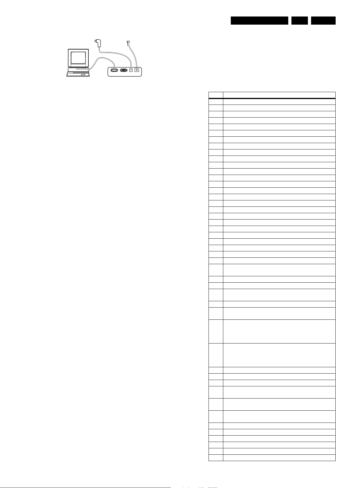
5.3.3 How To Connect
1. First, install the ComPair Browser software (see the Quick
Reference Card for installation instructions).
2. Connect the RS232 interface cable between a free serial
(COM) port of your PC and the PC connector (marked with
“PC”) of the ComPair interface.
3. Connect the mains adapter to the supply connector
(marked with “POWER 9V DC”) of the ComPair interface.
4. Switch the ComPair interface “OFF”.
5. Switch the television set “OFF” with the mains switch.
6. Connect the ComPair interface cable between the
connector on the rear side of the ComPair interface
(marked with “I2C”) and the ComPair connector at the rear
side of the TV.
7. Plug the mains adapter in a mains outlet, and switch the
interface “ON”. The green and red LEDs light up together.
The red LED extinguishes after approx. 1 second while the
green LED remains lit.
8. Start the ComPair program and read the “Introduction”
chapter.
Service Modes, Error Codes, and Fault Finding
Note: A fault in the protection detection circuitry can also lead
to a protection.
TO SERVICE
CONNECTOR
PC VCR I2CPower
9V DC
E_06532_008.eps
190204
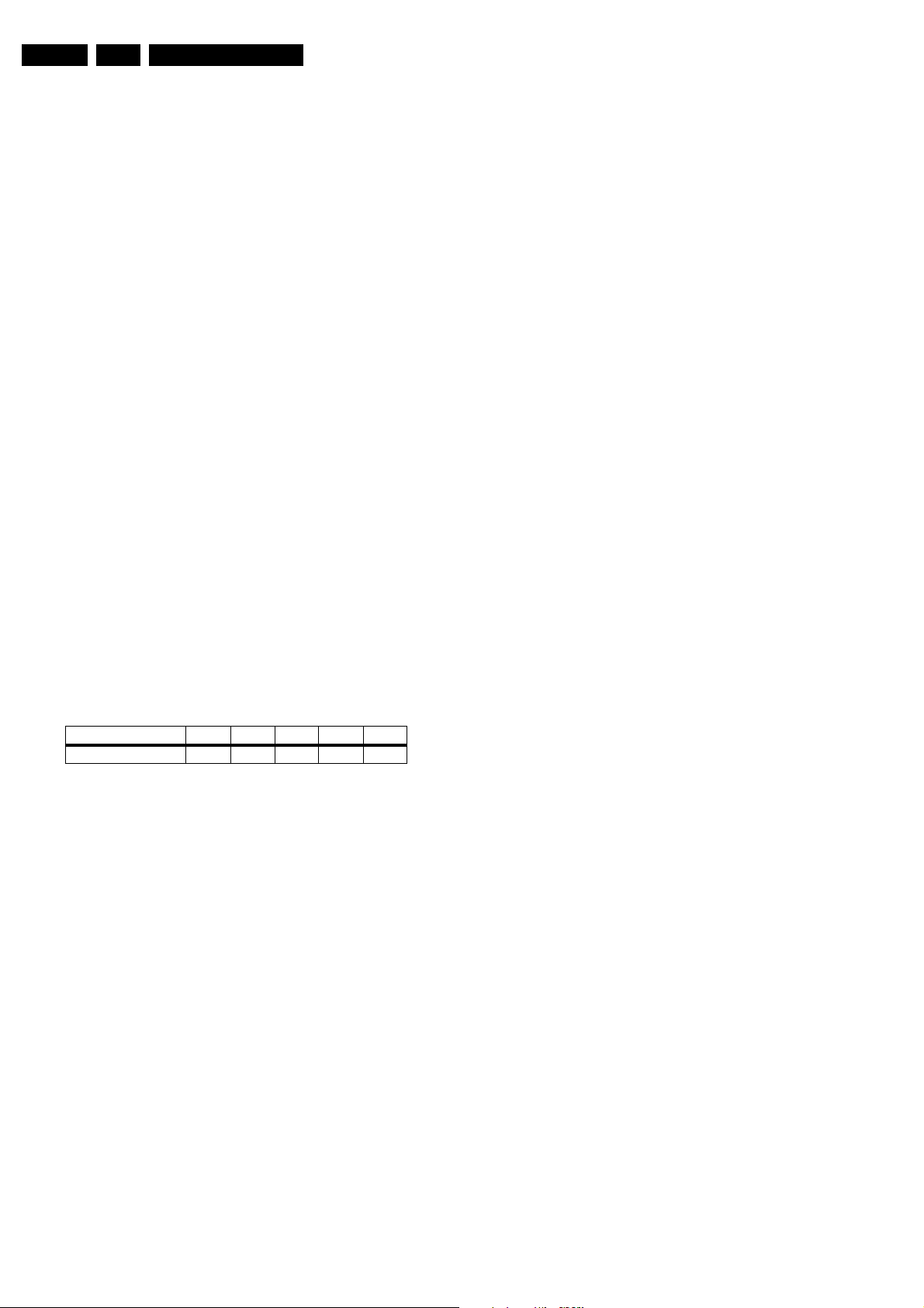
Error codes "01", "02", "03", and "04" are protection codes, and
in this case the supplies of some circuits will be switched "off".
Also in protection, the LED will blink the number of times
equivalent to the most recent error code.
Table 5-1 Error codes
EN 19EM8E 5.
Figure 5-1 ComPair Interface connection
5.3.4 How To Order
ComPair order codes (EU/AP/LATAM):
• Starter kit ComPair32/SearchMan32 software and
ComPair interface (excl. transformer): 3122 785 90450.
• ComPair interface (excluding transformer): 4822 727
21631.
• Starter kit ComPair32 software (registration version): 3122
785 60040.
• Starter kit SearchMan32 software: 3122 785 60050.
• ComPair32 CD (update): 3122 785 60070 (year 2002,
3122 785 60110 (year 2003).
• SearchMan32 CD (update): 3122 785 60080 (year 2002),
3122 785 60120 (2003), 3122 785 60130 (2004).
• ComPair interface cable: 3122 785 90004.
• ComPair firmware upgrade IC: 3122 785 90510 (only
useful for TV-sets with flashable software).
• Transformer (non-UK): 4822 727 21632.
• Transformer UK: 4822 727 21633.
Note: If you encounter any problems, contact your local
support desk.
5.4 Error Codes
5.4.1 Introduction
The error code buffer contains all errors detected since the last
time the buffer was erased. The buffer is written from the left to
the right. When an error occurs, which is not yet in the error
code buffer, the error code will appear at the left side and all
other errors shift one position to the right.
5.4.2 How to clear the Error Buffer
Use one of the following methods:
• Activate “Reset Error Buffer” in SAM menu
• If the content of the error buffer was not changed for 50+
hours, it resets automatically.
By leaving SDM or SAM via the power switch, the error buffer
will not be reset.
Examples:
ERROR: 000 000 000 : No errors detected
ERROR: 036 000 000 : Error code 036 is the last and only
detected error
ERROR: 018 036 000 : Error code 036 was first detected and
error code 018 is the last detected (newest) error
The contents of the error buffer can also be displayed by using
of the “blinking LED” procedure, if no picture is available. See
the chapter “The blinking LED procedure “below.
5.4.3 Error Code Definition
In case of non-intermittent faults, clear the error buffer before
you begin the repair. Make sure “old” error codes are not
present. If possible, check the entire content of the error
buffers. In some situations an error code is only the result of
another error code (and not the actual cause).
Error Description
1 (1) NVM (M24C32)
2 HFB protection
3 Picnic (SAA4978)
4 5VProtection
5 8V Protection
6 (2) Slow I2C bus blocked
8 HIP I/O-video processing (TDA9320)
9 Wireless Expander (PCF8574)
12 Topic (LT P Peaking) (TDA9178)
13 Tuner Protection
14 ITT Sound Processor (MSP3411/3412/3452)
15 3D Combfilter protection (mPD64083)
16 Feature Box Protection (FBX)
17 I/O Expander HD Interface (M62320P)
18 Fast I2C bus blocked
19 Auto Scavem DAC (TDA8444)
21 PIP I/O Expander (M62320P)
22 PIP BOCMA (TDA888X)
23 PIP Tuner
24 PIP Muppet (SAB9081)
25 PIP V-Chip (Z86130)
26 Falconic (SAA4992)
27 Eagle device
28 Back Current loop
32 Flash Ram (EPG)
36 Light engine shutdown Protection Error
37 Light engine shutdown protection. Spontaneous
blinking 37-37-37.
38 Lamp Failure.
39 Light engine polarizer fan failure, protection error.
41 Shutdown protection error, spontaneous blinking 41-
41-41. GDE not responding
42 Not protection error. GDE NVM error
43 Fan Fault. Not protection error. Shut down if error
exists continuously for 2 minutes
44 Ambient Temperature Warning. Not protection error.
Message should be displayed for 6 seconds and every
15 minutes as long as temp is above ambient temp.
warning
45 High temperature alert. Not protection error. Shut
down message should be displayed and system
should enter standby after 1 minute if the temperature
exceeds this limit.
46 Audio fault (audio board). N ot protection error.
47 Audio fault (audio board). N ot protection error.
48 Thermo cutoff SW. Protection error
49 Engine Fault Lamp Off. Unexpected Lamp Off.
System should enter into standby.
51 Main scaler not working. Communication via EPLD is
ok, scaler not responding. Not a protection error.
52 NVM error MSB Pixelworks (local error number
MSB=3),
53 Video switch. Local error number MSB=4
54 Audio switch (local error number MSB=5) (TEA6422D)
55 EPLD (local error number MSB=6)
56 ADC error (local error number MSB=7) (AD9888)
57 MSB I2C error. Not protection error
59 Reserved error codes for NAFTA Digital TV
EN 20 EM8E5.
Service Modes, Error Codes, and Fault Finding
(1) This error should start the Blinking LED procedure when it
occurs.
(2) This error has the highest priority, so if other errors occur
simultaneously, this should go first.
5.5 The Blinking LED Procedure
NOTE: Perform this procedure without any signal applied.
This is necessary because making any adjustment, such as
lowering the volume, will render the Blinking LED procedure
inoperative.
The contents of the error buffer can also be made visible
through the “blinking LED” procedure. This is especially useful
when there is no picture.
When the SDM is entered, the LED will blink the number of
times, equal to the value of any error codes.
The ON/OFF indicator turning orange for 500 ms precedes all
error code sequences (there is a possibility of up to 10).
After the 500 ms delay, the ON/OFF indicator will turn green for
1500 ms before the first code begins. If an error code is smaller
than 10, the ON/OFF indicator will rapidly flash orange 1-9
times to indicate the code (EXP. Six rapid flashes indicates an
error code of 6.)
There will be a delay, green light, of approximately 3 seconds
between codes.
For error codes of 10 and higher, the ON/OFF indicator will
slowly flash orange the correct number of times to indicate the
first digit, and then will rapidly flash orange the correct number
of times to indicate the second digit (EXP. Three slow orange
flashes followed by 6 rapid orange flashes indicate an error
code of 36.)
When all error-codes are displayed, the sequence is finished
and the ON/OFF indicator turns green for 3 seconds. At this
point the sequence will begin again as indicated by the ON/
OFF indicator turning orange for 500 ms.
approximately 3.3 V. This voltage can be measured on Pin 36
of 1205.
When the set is turned "On", the OTC will pull the Standby Line
Low. The relay on the Input Power board will then turn "On",
providing RAW_DC voltage to the Main Power board via Pin 1
of 1311. If 5 V is present on Pin 11 of 1403, Pin 1 and 3 of 1460,
and Pins 1 and 2 of 1410, the Standby line on Pin 9 of 1403 is
Low, RAW_DC should be present on Pin 1 of 1311. If it is not,
the Input Power board should be repaired or replaced.
When the RAW_DC voltage is applied to the Main Power
board, +36 V should appear on Pin 4 of 1312.
Additional voltage are 5 V on Pins 3, 4 and 5 of 1313, +9 V on
Pins 1 and 2 of 1314, +3.3 V on Pins 5 and 6 of 1314, and +12
V on 1314.
Operating voltages are applied to the Light Engine on
connector 1315.
5.6.2 Troubleshooting Audio Problems
The Audio Power supply is located on the Input Power board.
A positive 25 V should be present on Pin 1 of 1316 and a minus
25 V on Pin 4. An audio signal should be present on Pins 1 and
4 of 1700. The SOUND_ENABLE line should be High to switch
the Audio Amplifier "On".
5.6.3 Troubleshooting Video Problems
The 1fH signals from the SCART panel or Side Jack panel are
fed to the SSB for processing. The signal is fed to the Scaler
board in a digital format via 1401. (Figure 75) After processing,
the signal is fed to the Light Engine via connector 1200. The
SSB can be bypassed by selecting the inputs on the Scaler
board.
Table 5-2 Example of the blinking LED procedure
Error code position 1 2 3 4 5
Error buffer: 018 006 036 0 0
After entering SDM: The sequence will begin with 1 long blink
of 500 ms, then pause 1500 ms, then slowly blink once followed
by 8 rapid blinks (indicating error code 18), next the LED will
pause for 3 seconds followed by 6 rapid blinks (indicating error
code 6), next the LED will pause for 3 seconds, then slowly
blink 3 times followed by 6 rapid blinks (indicating error code
36), then pause 3 seconds ending the sequence in this
example. If there were error codes in positions 4 and 5, those
sequences would also be given.
5.6 Fault Finding
5.6.1 Troubleshooting a Dead Set
If the status lamp is Red, the 5 V supply is present and the OTC
is working. If the indicator LED is "Off", the Standby Supply may
not be working. The Standby Supply is located on the Main
Power Board. This voltage can be measured on Pin 2 of
connector 1312.
This voltage is then fed to the Input Power board on 1403, Pin
1. The 5 V Standby voltage is also fed to the Side Jack Panel
via Pin 4 of 1344. It is then fed back to the System board on Pin
5 of 1344 and then to the Input Power board on Pin 11 of 1403.
If the voltage on Pin 5 of 1344 is High, the +5V_STBY_SW
voltage is switched "On" and fed to the SSB via Pin 40 of
connector 1205.
The ON/OFF LED voltage is fed to the System board via Pin 77
of 1205. It is then fed to the LED Sensor Panel via Pin 5 of
1214. In the Standby mode, the Standby line will be

Block Diagrams, Testpoint Overview, and Waveforms
6. Block Diagrams, Testpoint Overview, and Waveforms
Not applicable yet
EN 21EM8E 6.
Circuit Diagrams and PWB Layouts
7. Circuit Diagrams and PWB Layouts
LCoS Audio Amplifier Board
EN 22EM8E 7.
1
A
B
C
D
E
F
TO SYSTEM
BOARD
(1700)
G
SOUND_ENABLE
H
I
J
K
L
M
N
3135_037_11411_01 X
RESERVED
O
Ref Des
P
9710 NOT USED
9711 NOT USED
3135 033 3353.3
1
2
3
47
LCOS AUDIO AMPLIFIER BOARD
I713
3702
6K8
5V2
5V2
I711
3701
10K
2739
100R
7701
0V
BC847B
A1
I707
2701
3793
100R
47n
2703
330n
330n
3790
100R
6708
6709
4
1700
B8B-EH-A
9711
8
NOT USED
7
6
5
4
AUDIO_R
3
2
1
AUDIO_L
1216
1
2
F702
TO SYSTEM
BOARD
E
N
A
U
F
R
T
O
A
P
E
X
NOT USED
3135_037_11411_01 RESERVED
2
9710
A2
2740
n
o
t
_
u
s
e
d
X
F700
100n
2729
F701
F703
3792
100R
47n
3791
319803690010
319803690010
3
F708
I750
5
I714
6704
6706
BAS316
BAS316
6705
6707
BAS316
BAS316
6710
2704
BAS316
6711
BAS316 BAS316
BAS316
NOTES
1. CAPACITANCE VALUES ARE IN F
m= MILI u= MICRO n= NANO p= PICO f= FEMT
2. RESISTANCE VALUES ARE IN OHMS:
R= OHM K= KILO M= MEGA G= GIGA T= TERA
3. SAFETY TRIANGLE REPRESENTS PCEC REPLA
4. FOR VALUE SEE TABLE.
*
5
6
3703
33K
10K
3704
I710
100n
2702
100n
10R
3705
I704
220n
2708
I702
220n
2720
1701
HEATSINK
123
2718
27p
3712
10K
I708
I712
A4
100n
2706
470p
2722
I751
2721
ARADS:
6
I709
4
I738
A3
3721
470p
2705
-23V1
26V
0V
0V
0V
5V1
-14V2
5V3
24V6
24V6
5K6
3722
68K
O
CEMENT PART ONLY.
7
8
2u2 50V
470p
2709
2710
I717
470p
I718
7700
TDA7490
14
CURREF
8
OSC
7
FEED1
9
FEED2
10
IN1
0V
18
IN2
17
0V
FEED3
19
0V
FEED4
6
STBY-MUTE
25
VREG
-VCCSIGNSUB
12
+5V
4
-VCCPOW1
+VCCPOW1
22
-VCCPOW2
+VCCPOW2
I715
3723
56K
8
913
3708
56K
5K6
3706
3707
68K
I719
3711
120K
220n
2723
0V
11
T1
5
9V2
BOOT1
3
0V
OUT1
OUT2
BOOT2
T2
NC1
GND
-5V
I732
0V
23
9V3
21
15
0V
20
13
1
-24V6
-5V4
16
-24V6
2
24
-24V6
2743
220n
220n
2732
9
10
BC847B
I736
2714
33n
I731
A6
A5
I739
2726
33n
I705
I703
2727
1n0
I742
2733
220n
220n
2724
2742
220n
10
11
7710
BC847B
5V1
5V1
0V
0V
7711
4V9
BC847B
4V9
I720
5V1
5V1
7707
0V6
I721
2719
2715
1n0
1n0
2716
330p
3710
22K
2728
330p
3725
22K
2707
100n
I746
I747
2711
1n0
3799
3714
I756
47K
3728
220R
I722
3709
220R
2744
220n
2712
2725
220n
220n
3724
220R
3729
220R
I723
BC857B
0V6
47K
2731
7706
I726
3713
2713
5701
68u
2745
220n
2m2
12
I757
3K3
3797
3716
47K
5V2
5V2
5V2
5V2
V06
V06
100R
I728
V06
V06
100n
I724
1311
1702
BT169B
2777
1412
I758
3798
3K3
I725
3715
47K
+5V
3K3
2735
3726
I727
4V7
4V7
6703
1N4148
2717
5716
680n
I743
5702
68u
1K0
3720
I735
1K0
2m2
2730
3719
F719
14
15 18
I730
10u 50V
I755
3727
47K
100p
10n
2737
5714
1u0
2780
5717
5713
5718
100n
1u0
1u0
1u0
15
3730
3717
2781
5V2
5V2
7705
BC847B
0V
0V
100R
F709
150K
16
5708
7704
BC847B
0V
0V
2776
47u 50V
I737
0V6
0V6
10K
3796
3718
150K
I733
1
1703
2
I734
1
10n
2736
1704
2
5715
2763
680n
F710
F712
F711
100n
F718
16
17 19
+5V
1n0
5707
17
F714
F716
F717
F715
F713
100R
1n0
2741
1321
A7
26-62-7051
F704
1K5
F705
F706
F707
A8
1K5
1316
1
+V_AUDIO
2
3
4
-V_AUDIO
B4P-VH
18
6702
1N4148
6701
1N4148
2734
5V2
5V2
I740
0V
0V
3731
0V3
0V3
7708
BC847B
3
3732
CM08
4
3
3733
CM08
4
24V6
-24V6
1305
+5V
1
GND
2
PWR_FAIL
3
PWRFAIL_STDBY
4
AUDIO_FAULT
5
GND
6
DC_FAULT
7
B7B-PH-K
FOR NAFTA
TO CENTER CHANNEL OR SPEAKERS
RIGHT+
1
RIGHT-
2
LEFT-
3
5
OR
LEFT+
FOR EUROPE
CONNECT TO THE SPEAKERS
TO INPUT
POWER BOARD
(1316)
19
(1349)
20
TO SYSTEM
BOARD
(1305)
E_14780_137.eps
130704
20
A
B
C
D
E
F
G
H
I
J
K
L
M
N
O
P
1216 J2
1305 C18
1316 K17
1321 H18
1700 H2
1701 F6
1702 F13
1703 G16
1704 H16
2701 G5
2702 H6
2703 I4
2704 I5
2705 E7
2706 I6
2707 I10
2708 K6
2709 F8
2710 F8
2711 J11
2712 I11
2713 F13
2714 H9
2715 F10
2716 G11
2717 F14
2718 G6
2719 F11
2720 K6
2721 K7
2722 J6
2723 G9
2724 K9
2725 I11
2726 I10
2727 J10
2728 H11
2729 F3
2730 L14
2731 K12
2732 L9
2733 K10
2734 C17
2735 E14
2736 H16
2737 H15
2739 H4
2740 I3
2741 F17
2742 L10
2743 K9
2744 G11
2745 I12
2763 J16
2776 E16
2777 G13
2780 K15
2781 L15
3701 E4
3702 E5
3703 D6
3704 E6
3705 J6
3706 F9
3707 F8
3708 E9
3709 F12
3710 H11
3711 F9
3712 H6
3713 E13
3714 E11
3715 D14
3716 D13
3717 G15
3718 G16
3719 L13
3720 K13
3721 J7
3722 K7
3723 J8
3724 J11
3725 I11
3726 E14
3727 F15
3728 F12
3729 J11
3730 D15
3731 E17
3732 G17
3733 H17
3790 H4
3791 I3
3792 I3
3793 G4
3796 G16
3797 B13
3798 B13
3799 D12
5701 G13
5702 J13
5707 F17
5708 C16
5713 L14
5714 J14
5715 I16
5716 G14
5717 K14
5718 L14
6701 B17
6702 B17
6703 F14
6704 H5
6705 H5
6706 H5
6707 H5
6708 I5
6709 J5
6710 I5
6711 J5
7700 H8
7701 E4
7704 E16
7705 D15
7706 D13
7707 F11
7708 F16
7710 B11
7711 D12
9710 H3
9711 G2
F700 E3
F701 G3
F702 I3
F703 H3
F704 H17
F705 H17
F706 H17
F707 H17
F708 G3
F709 F15
F710 J16
F711 K16
F712 K16
F713 D18
F714 B17
F715 C17
F716 B18
F717 B17
F718 L16
F719 L14
I702 K6
I703 J10
I704 J6
I705 I10
I707 G4
I708 H6
I709 E7
I710 F6
I711 E4
I712 H6
I713 E4
I714 E5
I715 J7
I717 F8
I718 F8
I719 F9
I720 D12
I721 F11
I722 F11
I723 L11
I724 G13
I725 D14
I726 E12
I727 E14
I728 E13
I730 D14
I731 H10
I732 H9
I733 G16
I734 H16
I735 L14
I736 G10
I737 F16
I738 G7
I739 H10
I740 E17
I742 K10
I743 J14
I746 J11
I747 J10
I750 I3
I751 J6
I755 F14
I756 E11
I757 B13
I758 B14
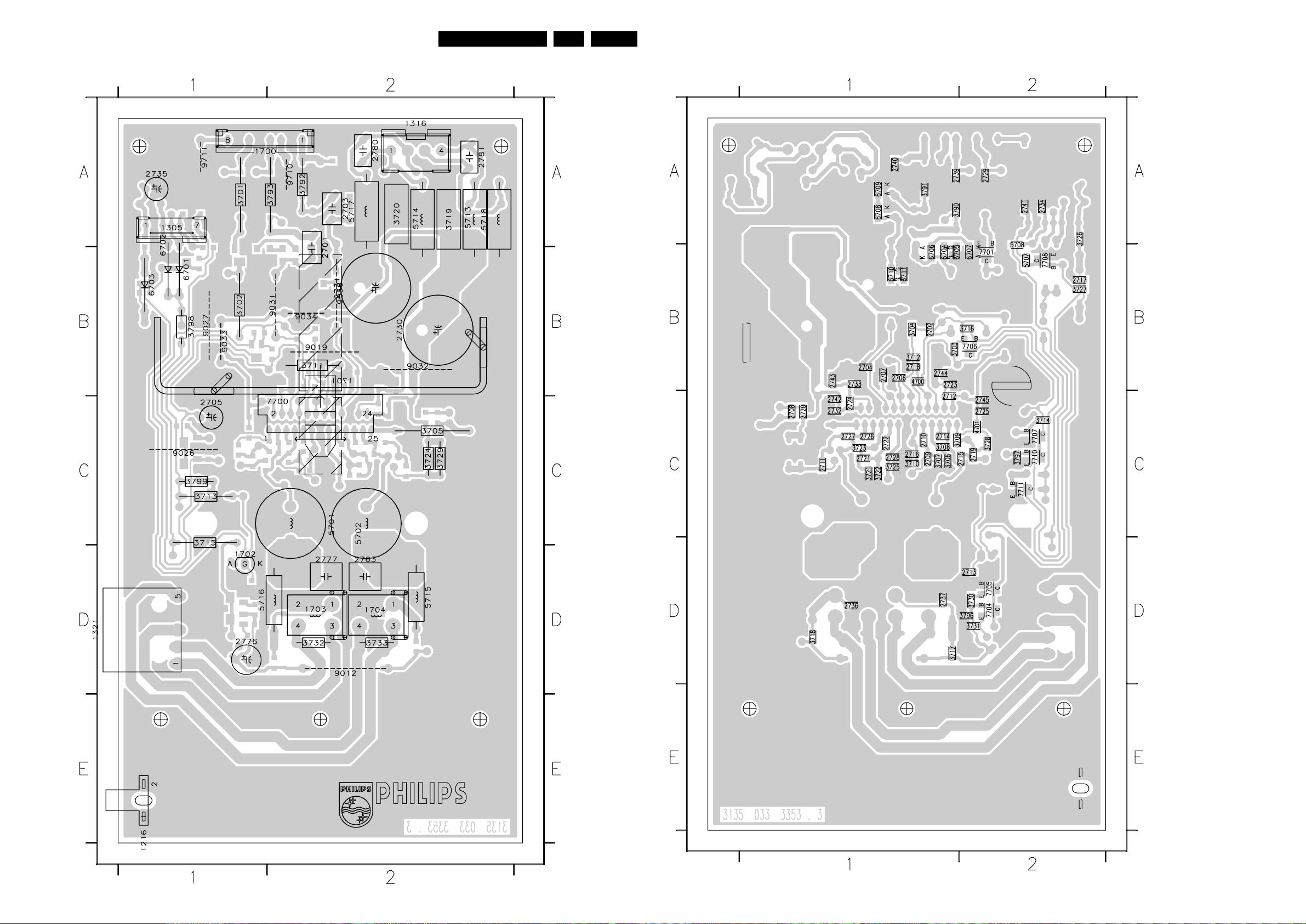
Circuit Diagrams and PWB Layouts
EN 23EM8E 7.
Layout LCoS Audio Amplifier Board (Top Side)
3135 033 3353.3
E_14780_078.eps
090704
1216 E1
1305 A1
1316 A2
1700 A1
1701 B2
1702 D1
1703 D2
1704 D2
2701 B2
2703 A2
2705 C1
2730 B2
2731 B2
2735 A1
2763 D2
2776 D1
2777 D2
2780 A2
2781 A2
3701 A1
3702 B1
3705 C2
3711 B2
3713 C1
3715 C1
3719 A2
3720 A2
3724 C2
3729 C2
3732 D2
3733 D2
3792 A2
3793 A2
3798 B1
3799 C1
5701 C2
5702 C2
5713 A2
5714 A2
5715 D2
5716 D1
5717 A2
5718 A2
6701 B1
6702 A1
6703 B1
7700 C2
9012 D2
9019 B2
9026 C1
9027 B1
9030 B2
9031 B2
9032 B2
9033 B1
9034 B2
9710 A2
9711 A1
Layout LCoS Audio Amplifier Board (Bottom Side)
3135 033 3353.3
E_14780_079.eps
120704
2702 B1
2704 B1
2706 B1
2707 B1
2708 C1
2709 C1
2710 C1
2711 C1
2712 C1
2713 D2
2714 C1
2715 C2
2716 C1
2717 B2
2718 B1
2719 C2
2720 C1
2721 C1
2722 C1
2723 B1
2724 C1
2725 C2
2726 C1
2727 C1
2728 C1
2729 A2
2732 C1
2733 B1
2734 A2
2736 D1
2737 D1
2739 A1
2740 A1
2741 A2
2742 C1
2743 B1
2744 B1
2745 C2
3703 B1
3704 B1
3706 C1
3707 C1
3708 C1
3709 C1
3710 C1
3712 B1
3714 C2
3716 B2
3717 D1
3718 D1
3721 C1
3722 C1
3723 C1
3725 C1
3726 A2
3727 B2
3728 C2
3730 D2
3731 D2
3790 A1
3791 A1
3796 D2
3797 C2
4700 B1
4701 C2
5707 B2
5708 B2
6704 B1
6705 B1
6706 B1
6707 B2
6708 A1
6709 A1
6710 B1
6711 B1
7701 B2
7704 D2
7705 D2
7706 B2
7707 C2
7708 B2
7710 C2
7711 C2
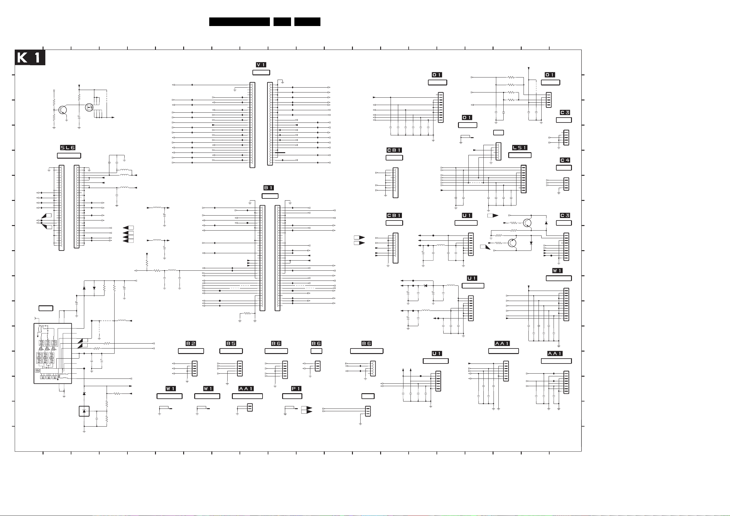
LCoS System Board
1
1
A
A
B
B
C
C
D
D
EE
F
F
GG
H
H
I
I
J
J
K
K
L
L
M
M
N
N
O
O
P
P
SDA-PW
SCL-PW
L-D1
3-D13
R-D1
3-D20
L-D2
3-D13
R-D2
3-D20
3-G20
3-H20
3135 033 3299.6
1
1
2
2
LCoS SYSTEM BOARD (1 OF 4)
VACATION_SW
4-C5,1-K18,1-E16,1-C17
10K
3103
10K
3104
I163
0V0
I164
0V0
0V0
I167
0V0
I170
C3
3V3
F134
F135
3V3
C4
MT1
52479-0640
TUNER
1203
UV1316-MK3
MT113MT2
L
H
M
L
H
M
MT315MT4
TUNER_GND
2
2
+5V_STDBY
7019
BC847B
SCALER (MSB)
1210-1
1210-2
ROW_A
ROW_B
A1
B1
A2
B2
A3
B3
A4
B4
A5
B5
A6
B6
A7
B7
A8
B8
A9
B9
A10
B10
A11
B11
A12
B12
A13
B13
A14
B14
A15
B15
A16
B16
A17
B17
A18
B18
A19
B19
A20
B20
A21
B21
A22
B22
A23
B23
A24
B24
A25
B25
A26
B26
A27
B27
A28
B28
A29
B29
A30
B30
A31
B31
A32
B32
52479-0640
MT2
TUNER_GND
12
AGC
1
TU
2
AS
3
SCL
4
SDA
5
6
NC1
VS
7
ADC
8
VST
9
PLL
IF2|NC2
10
IF1
11
14
TL431BCLP
3
3
3105
220K
4123
35V4u7
2128
I168
0V0
I171
0V0
I174
0V2
0V0
4-G15,3-L9,2-F18,1-C8,1-H13,1-I12,#3
4V
4-G15,3-M9,2-F18,1-C6,1-H13,1-I7,#3
4V
I192
I195
6102
6101
BAS316
I207
50V
2102
100u
F108
C2
C1
I209
2104
F109
32V3
6112
BZV85-C15
16V8
7115
1
K
2V4
R
3
A
2
3
3
Circuit Diagrams and PWB Layouts
6
Pr
CVBS-SC1_AV1-IN
R-SC1_AV-OUT
L-SC2_AV2-IN
SCL-EMG
L-Y2
L-Y1
AUDIO-SW
R-FRONT-IN
R-MSB
R-SC2-OUT
STATUS-SC3
SNDR-SC3-IN
5108
+8V6A
1u0
16V330u
2123
5109
+3V3A
1u0
2124
470u 10V
10K
100R
3101
SCL-EMG
SDA-EMG
2116
Y-COMB
C-COMB
CVBS-IN
5106
1n0
INPUT POWER
1217
0-106451-1
61
7119
SI4431ADY
5678
3-C13
3-C20
1-H11
1-H7
5V
2-I17,2-B20
2-I17,2-C20
5V
BAS316
4103
3111
47R
1n0
2103
2105
4
4
9002
+5V_STDBY_SW
2351
100n
100n
2352
+3V3
+12V
100n
2353
L-RGB
R-RGB
HFB
VFB
SDA-EMG
SCL-EMG
SDA-GDE
SCL-GDE
SOUND-ENABLE
10K
3K9
3107
3106
5101
4104
6u8
3110
4-G15,3-M9,2-F18,1-C6,1-H13,1-I7,#3
47R
4-G15,3-L9,2-F18,1-C8,1-H13,1-I12,#3
220u
3108
75R
3112
120K
10K
100n
3109
4
4
5307
5308
5309
2130
1u0 50V
1-G8
C1
C2
C5
C6
1-N19,1-C10
1-H7
+5V
IF-TER
PIP_TUNER_33V
+36V
5
5
SEL-SVHS-RR_STATUS2
4-G15,3-M9,2-F18,1-H13,1-I7,1-O11,#3
+5V2A
+9V
+8V6
+3V3
+5V_STDBY
3122
AGC
5
5
2-N14,1-F19
1-G12
1-J7
1-I7
1-H7
3-D13
3-D13
1-J12
1-C13,1-J12
3-F20
1-J7
1-N9
1-M9
SEL-SVHS-RR_STATUS2
470p
2101
EMG* 3D COMB
1-F13
1-F13
1-E13
1
2
7
7
I100
FBL-SC1-IN
I105
L-SC1_AV-OUT
I108
CENTER-IN
I112
R-SC2_AV2-IN
I115
4-G15,3-L9,2-F18,1-H13,1-I12,1-O11,#3
SDA-EMG
+9V
I121
R-Y2
I125
R-Y1
L-FRONT-IN
I133
L-MSB
I137
P50-W
I140
L-SC2-OUT
I144
SNDL-SC3-IN
I147
2-M13
B-SC1_U-IN
C-SC2_SVHS-IN
CVBS-TER-OUT
LIGHT-SENSOR
R-SC1_AV-OUT
HEADPHONE-L
1-C12
1-D12
1-J5
AGC
1-C6
1-G4
VFB
1-F16
4-G15,3-M9,2-F18,1-C6,1-H13,1-O11,#3
SCL-EMG
1-C6
L-SC2_AV2-IN
L-SC2-OUT
1-E8
1-E6
R-SC2-OUT
1-C6
1-E12,1-C13
Y-F RO N T-I N
1-C13,1-D8
L-FRONT-IN
3-K2
1-C12
L-CL_VL-OUT
4-J8
AUDIO- L
1-F16
ON-OFF-LED
1-E16
KEYBOARD
1303
B5B-PH-K
R-SC3_V-IN
1
G-SC3_Y-IN
2
B-SC3_U-IN
3
4
FBL-SC3-IN
5
INPUT POWER
1218
0-106451-1
7
7
8
1-G12
1-J12
4-J8
1-J11
3-D20
3-D20
1-C13,1-J7
3-F13
1-H12
1-J7
1-M9
I149
R-SC1_V-IN
CVBS-SC2_MON-OUT
I159
I165
I172
F137
F139
I204
EMG* SCART3
1-D10
1-E10
1-E12
1-D10
1
2
8
98
9
REAR JACK PANEL
1fH CINCH
1220-2
1220-1
ROW_B
ROW_A
IF-TER
0V0
I103
I107
I111
4V4
I114
4V4
4V
I116
4V
0V
I123
0V
0V
I127
0V
0V
I131
0V
0V
I135
4V4
4V4
I143
I146
MT1
2-M17
1-B12
1-N5
+8V6A
+5V
+3V3A
I179
I181
4125
4122
3113
10R
52479-0640
I151
F136
A1
A2
A3
A4
A5
A6
A7
A8
A9
A10
A11
A12
A13
A14
A15
A16
A17
A18
A19
A20
A21
A22
A23
A24
A25
A26
A27
A28
A29
A30
A31
A32
MT2
1205-A
ROW_A
87613-8001
AUDIO_GND
B1
B2
B3
B4
B5
B6
B7
B8
B9
B10
B11
B12
B13
B14
B15
B16
B17
B18
B19
B20
B21
B22
B23
B24
B25
B26
B27
B28
B29
B30
B31
B32
52479-0640
EMG*SSB
1
3
5
7
9
11
13
15
17
19
21
23
25
27
29
31
33
35
37
39
41
43
45
47
49
51
53
55
57
59
61
63
65
67
69
71
73
75
77
79
EMG* SCART3
1402
B5B-PH-K
1
SNDR-SC3-IN
2
3
SNDL-SC3-IN
4
5
CVBS-SC3-IN
STATUS-SC3
AUDIO AMPLIFIER
1216
1
2
106957
NOTES
1. CAPACITANCE VALUES ARE IN F
m=MILI u=MICRO n=NANO p=PICO f=FEMT
2. RESISTANCE VALUES ARE IN OHMS:
R=OHM K=KILO M=MEGA G=GIGA T=TERA
3. SAFETY TRIANGLE REPRESENTS PCEC REPLA
4. FOR VALUE SEE TABLE.
*
9
9
10
10
0V
0V
2V3
0V
0V
0V9
0V1
0V
1V
I124
1V4
I128
I132
0V
3-L2,1-I12
4V4
4V4
0V
CVBS-FRONT-IN
0V
I145
Note: See SSB Schematic B1 for
Voltages and Waveforms for
Connector 1205
1205-B
ROW_B
I150
2
4
6
8
10
12
14
I160
16
18
I162
20
22
24
26
28
30
32
34
I169
36
I173
38
40
42
44
46
48
50
I182
52
54
56
58
60
I194
62
64
66
F138
68
70
72
I200
74
F140
76
I203
78
80
87613-8001
1680
B6B-PH-K
1-E6
1-E8
1-D12
1-E6
KEYBOARD
1215
0-106451-1
ARADS:
10
10
EN 24EM8E 7.
1111 13
I101
I102
I104
I106
I110
I109
I113
1-I5,1-N19
SOUND-ENABLE
+9V
1-D19
C-PIP
1-M8
FBL-SC3-IN
1-M8
R-SC3_V-IN
L-SC1_AV1-IN
1-M8
G-SC3_Y-IN
2-N20
1-C12
1-C12
1-G4
1-F16,1-K18
4-G15,3-L9,2-F18,1-C8,1-H13,1-O11,#3
4-E15
1-C8
1-C13
4126
4123
1-C12
4-K8
1-H19
1
HA50
2
3
VA50
1-H19
4
5
6
1
C1
2
C2
O
CEMENT PART ONLY.
11
2-N10,1-F19
Pb
2-N17,1-F19
Y
1-G8
CVBS-SC2_MON-OUT
1-J11
R-CL_VL-OUT
1-J7
L-CL_VL-OUT
1-G11
Y-CVBS-SC2_AV2-IN
1-G7
C-SC2_SVHS-IN
I117
1-H11
SC1-STATUS
I122
1-D19
Y-CVBS-PIP
I126
1-G7
CVBS-TER-OUT
I130
1-M9
CVBS-SC3-IN
1-C13,1-J12
I134
C-FRONT-IN
3-M2,1-J12
I138
R-SC1_AV1-IN
1-C13,1-J7
I142
Y-F RO N T-I N
I148
1-M8
B-SC3_U-IN
G-SC1_Y-IN
1-B8
Y-CVBS-SC2_AV2-IN
1-C6
SC1-STATUS
1-E8
HFB
STANDBY
+5V_STDBY_SW
+3V3A
INT-EMG
3-L2,1-D10
1-C8
R-SC2_AV2-IN
3-M2,1-D12
FRONT-DETECT
1-D12,1-C13
1-C13,1-D6
3-M2
R-CL_VL-OUT
1-D6
AUDIO- R
1-F16
EMG*
1681
B3B-PH-K
I2S_DATA_IN
1
I2S_DATA_OUT
2
3
4-G15,3-L9,2-F18,1-C8,1-H13,1-I12,#3
SDA-EMG
SCL-EMG
4-G15,3-M9,2-F18,1-C6,1-H13,1-I7,1-L5,#2
12
12
FRONT-DETECT
FBL-SC1-IN
CVBS-SC1_AV1-IN
STAT1_AFT_PIP-50-60HZ
P50-W
C1
4-G15,3-L9,2-F18,1-C8,1-I12,1-O11,#3
C2
4-G15,3-M9,2-F18,1-C6,1-I7,1-O11,1-L5,#2
SDA-EMG
L-SC1_AV1-IN
L-SC1_AV-OUT
R-SC1_AV1-IN
C-FRONT-IN
R-FRONT-IN
HEADPHONE-R
AUDIO-SW
RC5
EMG* AUDIO DELAY
2-C9
2-C1
I118
2-M10
I2S_CLK
I119
12
13
+8V6
Y-F RO N T-I N
C-FRONT-IN
L-FRONT-IN
R-FRONT-IN
CVBS-IN
C-COMB
Y-COMB
SDA-EMG
SCL-EMG
05FMN-BTK-A
PWRFAIL_STDBY
I I C
1244
B3B-EH-A
13
13
+9V
+5V
+5V
1683
PWR_FAIL
1
2
3
14
14 19
15
15
16
HP_OUT_L
3-M13
17
17
SIDE JACK
1335
1-E12,1-J7
1-D12,1-J12
1-D8,1-J7
1-J11
1-D6,1-J12
B11B-EH-A
1
2
3
4
5
6
7
8
9
10
11
1n0
1n0
2354
2357
100p
2355
2356
100p
1n0
1n0
2359
2358
HP_OUT_R
VACATION_SW
SIDE JACK
1337
0-106451-1
3-N13
4-C5,1-K18,1-E16,1-B2
1
2
+5V
2362
I T V
1245
95003-2661
1n0
3D COMB
1008
09JL-BT-E
1-M6
1-M6
1-M6
1
2V8
2
3
4
5
6
1V5
7
8
0V9
9
101112
13
3D COMB
1009
09JL-BT-E
1
+15V_STBY
4V1
2
+5V2A
3
4V1
4
+5V
5
8V9
6
7
8
9
12
10
11
13
+9V
+8V6
+3V3
2114
F102
F103
2110
100n
2111
470u 16V
F104
10V2m2
2115
100n
2113
VACATION_SW
KEYBOARD
LAMP_FAULT
ON-OFF-LED
LIGHT-SENSOR
F101
16V
1m0
6105
SB140
5104
1u0
+12V
STANDBY
F100
2112
2108
RC5
+9V
F105
4-C5,1-K18,1-B2,1-C17
1-K7
1-K7
4-H5
1-I11,1-K18
1-K12
1-I7
5102
1u0
1n0
100n
5103
1u0
100n
2109
2m2 25V
1n0
2381
2380
1n0
2369
MAIN POWER
+5V2
1n0
2370
2371
+9VR
1n0
2379
9001
1n0
2368
1313
B8P-VH
1
2
3
4
5
6
7
8
MAIN POWER
1314
B9P-VH
1
2
3
4
5
6
7
8
9
1n0
1n0
1n0
2367
2366
4-G15,3-L9,2-F18,1-C8,1-H13,1-I12,#3
SDA-EMG
C1
+5V
3121
100K
3120
+5V
47K
C2
SCL-EMG
4-G15,3-M9,2-F18,1-C6,1-H13,1-I7,#3
DC_FAULT
THERMO_CUTOFF
DOOR_INTERLOCK
STANDBY
VACATION_SW
AUDIO AMPLIFIER
1
2
3
4
5
4-E5,2-J8,1-M17
4-F5,2-J8,1-M17
14
1412
+5V_STDBY
2388
1n0
+33V
MAIN POWER
1312
B7B-EH-A
F106
1n0
1n0
2386
2387
15
15
1
2
3
4
5
6
7
1n0
2385
PWRFAIL_STDBY
AUDIO_FAULT
16
16
PWR_FAIL
DC_FAULT
+5V
4-E5,2-J8,1-N13
4-F5,2-J8,1-N13
2-F11
1-J18
2127
17
17 18
1n0
1n0
2129
2125
1n0
1n0
2126
AUDIO_GND
18
18
3114
56R
3115
56R
3116
56R
3117
56R
1n0
2363
1
2
3
4
5
LED SENSOR
6
1n0
2365
2364
3118
47K
3119
100K
1-N17
4-D5
4-E5
1-I11,1-F16
4-C5,1-E16,1-B2,1-C17
+5V
1305
B7B-PH-K
1
2
3
4
5
6
7
SOUND-ENABLE
18
1n0
B10B-EH-A
7023
BC847B
+5V_STDBY
1214
+5V_STDBY
L
R
1-I5,1-C10
1916
4117
1n0
2361
2360
Y-CVBS-PIP
1
2
3
4
5
6
7
8
9
10
7022
BC847B
6114
VA50
BAS316
HA50
+8V6
PIP_TUNER_33V
1n0
2378
2376
1n0
2377
4-J16
4-K16
2383
AUDIO_GND
19
19
SIDE JACK
1344
B5B-EH-A
1
2
3
4
5
1n0
1-D10
C-PIP
1-D12
2-N10,1-B12
Pb
2-N17,1-B12
Y
2-N14,1-B6
Pr
6113
BAS316
1-M11
1-M11
+5V
F107
INPUT POWER
1n0
1n0
2374
1n0
2372
2375
AUDIO AMPLIFIER
I120
I129
1n0
1n0
2382
2384
E_14780_113.eps
20
20
PIP MOD
B5B-EH-A
PIP MOD
B4B-EH-A
PIP MOD
B10B-EH-A
4V0
B12B-EH-A
1n0
B8B-EH-A
1n0
20
20
1200
1207
1201
1403
1700
1
2
3
4
5
1
2
3
4
1
2
3
4
5
6
7
8
9
10
1
2
3
4
5
6
7
8
9
10
11
12
1
2
3
4
5
6
7
8
130704
A
A
B
B
C8C
D
D
E
E
F
F
G
G
H
H
I
I
J
J
K
K
L
L
M
M
N
N
O
O
P
P
1008 E14
1009 H14
1200 D20
1201 H20
1203 K2
1205-A G9
1205-B G10
1207 F20
1210-1 E2
1210-2 E3
1214 E18
1215 N10
1216 N9
1217 N6
1218 N7
1220-1 B9
1220-2 B9
1244 N13
1245 D17
1303 M7
1305 M18
1312 M15
1313 H16
1314 J16
1335 B15
1337 D16
1344 B19
1402 M8
1403 J20
1680 M10
1681 M11
1683 M13
1700 M20
2101 J6
2102 K3
2103 M4
2104 M3
2105 O3
2108 J15
2109 J15
2110 J14
2111 J14
2112 I15
2113 K14
2114 I15
2115 K14
2116 J6
2123 G6
2124 I6
2125 N17
2126 N17
2127 N17
2128 C3
2129 N17
2130 J4
2351 E4
2352 E4
2353 F4
2354 D14
2355 D14
2356 D14
2357 D14
2358 D15
2359 D15
2360 C19
2361 C18
2362 C17
2363 C17
2364 G18
2365 G17
2366 G17
2367 G17
2368 G16
2369 G16
2370 I16
2371 I16
2372 L19
2374 L19
2375 L19
2376 L19
2377 L18
2378 L18
2379 L16
2380 L16
2381 L15
2382 N19
2383 N19
2384 N19
2385 N15
2386 N14
2387 N14
2388 N14
3101 I6
3103 C2
3104 C2
3105 C3
3106 J4
3107 J4
3108 N4
3109 O4
3110 L4
3111 L3
3112 O4
3113 K9
3114 B18
3115 B18
3116 B18
3117 C18
3118 G18
3119 H18
3120 H17
3121 H17
3122 I5
4103 L4
4104 K4
4117 B19
4122 J8
4123 J11
4125 J9
4126 J10
5101 K4
5102 H15
5103 J16
5104 K15
5106 I6
5108 G6
5109 H6
5307 E4
5308 F4
5309 F4
6101 J3
6102 J3
6105 J15
6112 N3
6113 H19
6114 H18
7019 C2
7022 G19
7023 H18
7115 N3
7119 C3
9001 F17
9002 C4
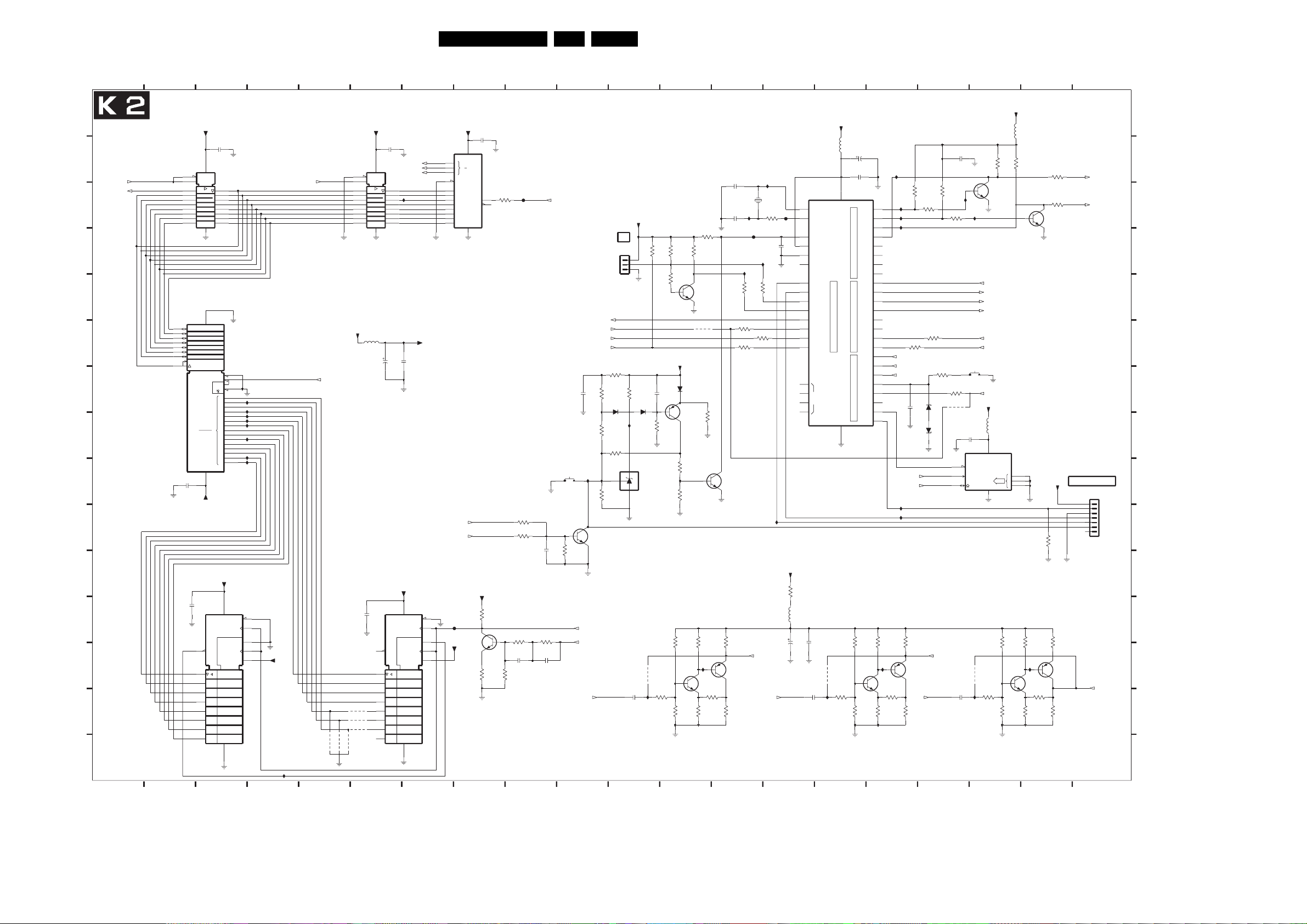
Circuit Diagrams and PWB Layouts
EN 25EM8E 7.
LCoS System Board
3227
4K7
4K7
3240
1K0
I261
7001
BC847B
270R
3220
470R
13
13
2309
27p
2308
I231
27p
F112
I237
3330
100R
3339
100R
3328
100R
4K7
7025
BC847B
1K0
3209
1-G7
7005
BC857B
1K0
3214
13
149
1412
I224
12M
1600
DSX840GA
I236
3314
3315
100R
B-SC1_U-IN R-SC1_V-IN
21
F113
3333
20
33R
10
35
2213
100p
32
33
11
100R
15
16
17
18
19
1
12
23
34
I257
+9V
10R
3395
8u2
5317
16V22u
2219
1-F19,1-B6
14
2391
2209
7108
P89C668
XTAL1
XTAL2
RST
EA_|VPP
PSEN_
ALE
RXD
TXD
INT0_
INT1_
T0|CEX3
T1|CEX4
WR_
RD_
NC
100n
2u2
15
15
+5V
5301
4422
VCC
PORT3
VSS
3207
4131
3226
I260
10R
3218
15
2307
10u50V
2302
100n
AD0
AD1
AD2
AD3
AD4
PORT0PORT1PORT2
AD5
AD6
AD7
T2
T2EX
ECI
CEX0
CEX1
CEX2
SCL
SDA
A8
A9
A10
A11
A12
A13
A14
A15
3212
100K
39K
3224
16
16
I213
I229
43
I232
42
I234
41
40
39
38
37
36
2
313
414
5
6
7
8
9
24
A
2-B7
25
B
2-B7
26
C
2-B7
27
28
29
30
31
SCL-GDE
SDA-GDE
I255
I256
1K0
3213
I259
7003
BC847B
3225
100R
3216
330R
16
16 17
3306
3309
100R
2215
1K0
7007
BC857B
1K0
1n0
17
17
4K7
4K7
3307
3319
3320
4K7
4K7
4-G15,3-M9,1-I17,1-H4,1-L5,1-O11,1-I7,#2
3308
100R
3228
1K0
3233
100R
4129
6201
PDZ6.8-B
6202
PDZ6.8-B
1-H4,2-C20
1-H4,2-B20
1-G8
1-F19,1-B12
17 18149
18
+5V
5315
2390
100n
I230
3-K19
3-K19
3-M19
3-L19
4-G15,3-L9,1-G18,1-H4,1-L5,1-O11,#3
1204
SKQNAB
2303
100n
7
WC
6
SCL
5
2208
I264
2u2
I233
3-C8
EEPROM
4132
3322
7008
BC847B
S_DATA_OUT
SHIFT_CLK
ADC_SEL
S_DATA_IN
SCL-EMG
SDA-EMG
POL_FAN_FAULT
+5V
5316
7107
M24C32-WMN6T
8
?
(4Kx8)
ADR
4
3204
10R
4K7
3323
0
1
2SDA
3206
100K
27K
3221
18
19
19
4K7
3311
100R
3316
100R
7009
BC847B
1
2
3
3210
3222
1K0
I262
7002
BC847B
150R
3223
180R
+5V
4K7
3321
1K0
3211
7006
BC857B
1K0
3215
19
1-H4,2-I17
SDA-GDE
1-H4,2-I17
SCL-GDE
PROGRAMMING
1241
B7B-EH-A
1-G11
G-SC1_Y-IN
E_14780_114.eps
20
2015
203
1
2
3
4
5
6
7
ENABLE
TXD
RXD
RST
130704
1
A
A
B
B
2-C5,2-G5,2-L10
CLK
I2S_DATA_OUT
C
C
D
D
E
E
F
F
G
G
H
H
I
I
J
J
K
K
L
L L
M
M
N N
N
O
O
1-M12
21
LCoS SYSTEM BOARD (2 OF 4)
1
11
2
3
4
5
6
7
8
9
CY7C199-15ZC
19
18
17
16
15
13
12
11
2202
100n
3135 033 3299.6
1
2
2
7104
74HCT573
7103
A,1D
A
2201
9
15
1
2
3
4
5
6
7
EN
C1
1D
32kx8
3 183
+5VD
2203
100n
20
19
18
17
16
15
14
13
12
10
14
20
G2
27
2C1
22
2EN
10
14
9
13
8
12
7
11
6
10
5
9
4
8
32k-1
3
A
7
0
2
6
1
5
26
4
25
3
24
2
23
1
21
0
RAM
28
+5VD
+5VD
7101
100n
TC74HC590AF
16
EN3
C2
CTR8
G1
(CT=255)Z4
4
1+
CT=0
2D3
8
3
4 2010
4
2-C5,2-C1,2-L10
I239
I241
I242
I243
I244
I248
I253
I254
14
13
12
11
10
+5VD
I266
4
4
5
2-C1,2-G5,2-L10
CLK
5125
100R
95
F111
3232
3230
1-M12
3244
4K7
3389
4K7
2217
3202
3231
1K0
3K9
2210
2216
82p
82p
1K0
6
6
+5VD
2204
100n
7105
20
74HCT573
1
EN
11
C1
2
1D
3
4
5
6
7
8
9
10
+5V
5302
50V10u
2211
CLK
100n
2206
9
4
15
1
2
3
4110
4
4111
5
4112
6
4113
7
4115
4114
6
6
19
18
17
16
15
14
13
12
+5VD
16
(CT=255)Z4
2D3
I217
2212
7102
TC74HC590AF
CTR8
8
100n
CT=0
EN3
C2
A
B
C
G1
1+
7
7
2-F16
2-G16
2-G16
+5VD
PWRFAIL_STDBY
14
13
12
11
10
71
7
11
10
9
7
4
3
2
1
15
14
13
12
PWR_FAIL
F110
+5VD
0
G
1
2
EN
0
1
2
3
4
5
6
7
+5VD
16
MUX
0
7
8
4-F5,1-M17,1-N13
4-E5,1-N13,1-M17
7004
BC847B
8
8
2205
100n
7106
CD74ACT151M96
5
6
+5VD
3201
470R
22R
3229
8
8
I2S_DATA_IN
1202
SKQNAB
1n0
3388
2-C5,2-C1,2-G5
1-M12
10
PWM_DRIVE
SYS_TACH
SYS_FAN_FAULT
AUDIO_FAULT
2218
100n
I258
7016
BC847B
4K7
CLK
I2S_CLK
Pb YPr
10
11
112
+5V
I R
1243
3235
680R
1K2
3237
2K2
3243
1-F19,1-B12
B3B-EH-A
3234
100R
6304
3238
220K
1
2
3
3-H6
3-I2
3-G6
1-M17
3
I250
R
3236
7109
TL431BCLP
1
K
A
2
2207
2u2
560R
10K
3334
3390
3332
100n
2214
6305
BAS316BAS316
3239
100K
4130
3203
I263
10R
11 1913
4K7
3331
4K7
7010
BC847B
4128
+5V
6306
BAS316
7024
BC857B
22K
3241
22K
3242
3205
3208
100K
39K
3217
3219
12
A
A
B
B
C
C
D
D
E
E
F
F
G
G
H
H
I
I
J
J
K
K
L
M
M
N
O
O
1202 I10
1204 G17
1241 I20
1243 D11
1600 C13
2201 L2
2202 I2
2203 B3
2204 B6
2205 B8
2206 L6
2207 M11
2208 M17
2209 M14
2210 M9
2211 G6
2212 G6
2213 D14
2214 G11
2215 H16
2216 M9
2217 K9
2218 G10
2219 L14
2302 C15
2303 H17
2307 B15
2308 C13
2309 C13
2390 B17
2391 L14
3201 L8
3202 L9
3203 M11
3204 M18
3205 L12
3206 L18
3207 L15
3208 L12
3209 L13
3210 L18
3211 L19
3212 L15
3213 L16
3214 N13
3215 N19
3216 N16
3217 N12
3218 N15
3219 N12
3220 M12
3221 N18
3222 N18
3223 M18
3224 N15
3225 M16
3226 M15
3227 D12
3228 G17
3229 M8
3230 M8
3231 L9
3232 C8
3233 G17
3234 G10
3235 G10
3236 G11
3237 H10
3238 H10
3239 H11
3240 H12
3241 I12
3242 I12
3243 I10
3244 J9
3306 C16
3307 C17
3308 F16
3309 F16
3311 C19
3314 E13
3315 F13
3316 C19
3319 C16
3320 C17
3321 J19
3322 B18
3323 B18
3328 F13
3330 E13
3331 D12
3332 E11
3333 C13
3334 D11
3339 F13
3388 K9
3389 J9
3390 D11
3395 K14
4110 N6
4111 N6
4112 N6
4113 O5
4114 O5
4115 O6
4128 F12
4129 G17
4130 M11
4131 M14
4132 M17
5301 B15
5302 F6
5315 B18
5316 H17
5317 L14
6201 H16
6202 H16
6304 G10
6305 G11
6306 G12
7001 M12
7002 M18
7003 M16
7004 L8
7005 M13
7006 M19
7007 M16
7008 C18
7009 C19
7010 E12
7016 J10
7024 H12
7025 I13
7101 L3
7102 L7
7103 E3
7104 B3
7105 B6
7106 B8
7107 H18
7108 C14
7109 I11
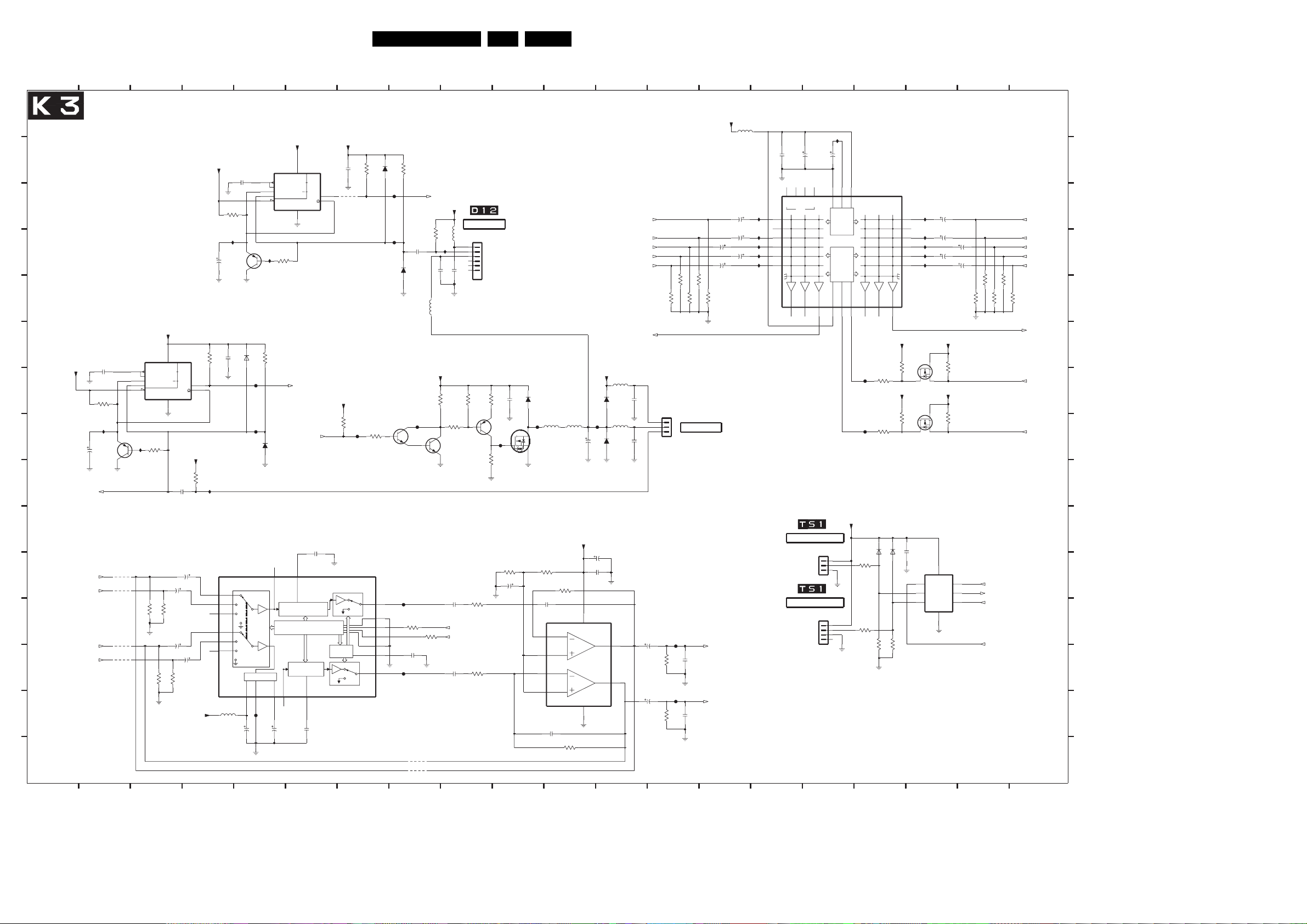
LCoS System Board
1
1
A
A
A
B8B
C
C
C
D
D
E
E
E
F
F
F
G
G
G
H
H
H
I
I
I
J
J
J
K
K
K
LDL
L
M
MBM
N
N
N
O
O
O
3135 033 3299.6
1
1
1
23
LCoS_SYSTEM_BOARD (3 OF 4)
2324
+5V
100n
3347
1M0
I292
50V1u0
BC857B
2325
2-F11
SYS_TACH
HEADPHONE-L
1-J7
L-SC1_AV1-IN
1-I12,1-D10
HEADPHONE-R
1-J12
R-SC1_AV1-IN
1-J12,1-D12
2
Circuit Diagrams and PWB Layouts
5
5
3342
1M0
I290
BC857B
7017
100n
7116
2106
100n
6110
INPUT
SELECTOR
SUPPLY
VS
16
2316
5
BAS316
F129
F128
AGND
715
F118
16V100u
AUDIO_GND
543
5
3346
6111
7118
NE555D
COMP
5
U
AU
6
X
2
Y
4
R1
3357
I291
1K0
100K
2-F11
BAS316
1
RECL
VOLUME+
LOUDNESS
SERIAL BUS DECODER
CREF
RECR
10
16V22u
2317
6
+5V +5V
8
RX>U
U
Y<
S
2
3
1
7
1
1
SYS_FAN_FAULT
2-F11
PWM_DRIVE
SYS_FAN_TACH
2319
100n
19
LOUDL
+ LATCHES
SOFT
MUTE
VOLUME+
LOUDNESS
LOUDR
12
100n
2318
6
62
7
7
10K
3358
2117
100n
4121
+5V
4K7
3350
F127
OUTL 2
MUTE
SDA
MUTE
7
7
3351
100K
3359
6103
100K
BAS316
F132
2-G18
F133
2120
100n
6104
BAS316
5312
F126
7011
BC847B
F114
6DGND
4
5SCL
8ADDR
3CSM
9OUTR
4-G15,2-F18,1-G18,1-H4,1-L5,1-O11,#3
3305
100R
3329
100R
4-G15,2-F18,1-I17,1-H4,1-L5,1-O11,#3
2331
22n
F115
4101
4102
8
8
3
3
+5V
7111
NE555D
8
COMP
5
U
AU
6
Y<
X
2
Y
4
R1
1
3349
I297
7015
1K0
4108
3302
560R
AUDIO_GND
3303
2313
4u7 35V
3301
560R
3304
560R
AUDIO_GND
4109
4116
4118
3
4
41
4
+5V
2107
1u0 50V
10K
2323
3348
RX>U
U
S
2
3
1
7
1
+12V
10K
3345
2322
I303
100n
2312
2314
35V4u7
2315
4u7
560R
TDA7309D-TR
35V4u7
17 IN1L
18 IN2L
20 IN3L
14 IN1R
13 IN2R
11 IN3R
35V
5305
+9V
2u2
4
4
POL_FAN_FAULT
+12V
10K
3360
5311
I296
2121
100n
2122
+12V
10K
3352
3353
3K3
7012
BC847B
2336
470n
SDA-EMG
SCL-EMG
2338
470n
9
9
LIGHTENGINE
1252
BM06B-SRSS-TBT
1
2
3
4
5
6
100n
78
10K
3354
AUDIO_GND
3313
10K
3335
10K
9
9
3355
3356
220R
7013
BC857B
F125
1K2
EN 26EM8E 7.
1210
2326
8
VSS
4
F123
25V220u
2389
16V 100u
2345
100n
+12V
6108
6109
OUTA
OUTB
12
L-RGB
L-Y1
L-Y2
L-D1
L-D2
L-MSB
5304
2301
100n
BAS316
5303
100n
2306
BAS316
1
16V 100u
7
12
12
12 13
11
11
10
10
100n
2321
6302
7014
STD3NK60Z
3312
3K3
2343
100u 16V
10 1413
10
11
BAS316
5313
5310
F124
8u2
330u
+5V
3317
3K3
3318
68K
2344
100p
7117
TDA1308
2
3
6
5
INA_NEG
INA_POS
INB_NEG
INB_POS
2396
100p
VDD
3336
68K
1111 15
18
14
14
3376
10K
3382
1-B17
6n8
AUDIO_GND
1-B17
6n8
AUDIO_GND
10K
3374
HP_OUT_L
HP_OUT_R
149
+9V
2330
4u7
2332
2333
4u7
2334
4u7
2335
4u7
4u7
10K
14118
138613
1312
1-G4
1-D6
1-D6
1-F1
1-G1
10K
3381
10K
3380
1-D8
1251
B3B-EH-A
1
2
SYSTEM FAN
3
F116
2392
10K
2393
3338
F117
2394
100u16V
10K
3337
2395
13
5306
I271
I275
I278
I281
I282
15 1716
15
15
100n
2328
22
NC321NC4
NC
L1
L2
L3
L4
L5
L6
LOUT3
16
THERMAL SENSOR
THERMAL SENSOR
8
LOUT2
14
22u
NC17NC2
1262
B3B-PH-K
1
2
3
1261
B4B-PH-K
1
2
3
4
LOUT1
12
2327
4
5
6
9
10
11
15
15 16
16
16
16
16
17
17
I270
22u
2329
3
2
1
GND
SUPPLY
DECODER
ADDR
26
CAP
BUS
SCL27SDA
+5V
7113
TEA6422
VS
ROUT3
15
17
28
F119
3365
100R
F120
3366
100R
6106
6107
BAS316
3340
100R
3341
100R
3343
3344
100K
17
17
18 19 20
18
2337
I272
R1
25
R2
24
R3
23
R4
20
R5
19
R6
18
ROUT113ROUT2
+5V +3V3
BSN20
10K
3392
+5V
10K
3102
2320
BAS316
100K
7121
312
7120
BSN20
3
100n
4u735V
2339
I276
4u735V
I277
2341
I279
4u735V
I280
3393
+3V3
1
3391
2
7110
8TLC0832CD
1
CLK
CS_
VCC|REF
2
CH0
3
CH1
GND
4
18
18
1814
19
19
2340
35V 4u7
2119
35V 4u7
10K
3377
10K
10K
3383
3379
10K
10K
2-E18
7
SHIFT_CLK
2-E18
6
DO
DI
S_DATA_OUT
2-E18
5
S_DATA_IN
2-E18
ADC_SEL
1917
19519
1-G4
1-D8
1-D8
1-F1
1-G1
10K
3384
10K
3385
1-D6
1-G1
1-G1
E_14780_115.eps
20
20
R-RGB
R-Y1
R-Y2
R-D1
R-D2
R-MSB
SDA-PW
SCL-PW
20
20
20
130704
A
A
A
B
B
B
C
C
C
D
D
D
E
E
E
F
F
F
G
G
G
H
H
H
II
I
J
J
J
KK
K
L
L
L
M
M
M
N
N
N
O
O
O
1251 G13
1252 D9
1261 L16
1262 J16
2106 C5
2107 D4
2117 B7
2119 D18
2120 D8
2121 E8
2122 E9
2301 G12
2306 H12
2312 K4
2313 K3
2314 L3
2315 M4
2316 N5
2317 N5
2318 N6
2319 J6
2320 K17
2321 G10
2322 I4
2323 F4
2324 G2
2325 H2
2326 H11
2327 B15
2328 B15
2329 B16
2330 C14
2331 M8
2332 D14
2333 D14
2334 D14
2335 D14
2336 K9
2337 C18
2338 M9
2339 D18
2340 D18
2341 D18
2343 K10
2344 K10
2345 K11
2389 K11
2392 L12
2393 M13
2394 M12
2395 N13
2396 N10
3102 H17
3301 L3
3302 L3
3303 M3
3304 M3
3305 L8
3312 K10
3313 K9
3317 K10
3318 K11
3329 L8
3335 M9
3336 N11
3337 N13
3338 M13
3340 K16
3341 L16
3342 C4
3343 L17
3344 L17
3345 I4
3346 F5
3347 G2
3348 F4
3349 H3
3350 H7
3351 H7
3352 G8
3353 H9
3354 G9
3355 G9
3356 I9
3357 D5
3358 B7
3359 B8
3360 D8
3365 G17
3366 H17
3374 E13
3376 E13
3377 E19
3379 E18
3380 E13
3381 E13
3382 E13
3383 E19
3384 E19
3385 E19
3391 H18
3392 G17
3393 G18
4101 O8
4102 O8
4108 K2
4109 K2
4116 L2
4118 M2
4121 C7
5303 H12
5304 G12
5305 N4
5306 B14
5310 H10
5311 D9
5312 E8
5313 H11
6103 B7
6104 E8
6106 K17
6107 K17
6108 G11
6109 H11
6110 F5
6111 H5
6302 G10
7011 H8
7012 H8
7013 H9
7014 H10
7015 H2
7017 D5
7110 K18
7111 F3
7113 C17
7116 K5
7117 L11
7118 B6
7120 G17
7121 F17

LCoS System Board
1
A
B
C
D
E
F
G
H
I
J
K
Circuit Diagrams and PWB Layouts
2 14
3
54
76
EN 27EM8E 7.
9
10 11
13128
LCoS SYSTEM BOARD (4 OF 4)
VACATION_SW
1-C17,1-B2,1-E16,1-K18
THERMO_CUTOFF
DOOR_INTERLOCK
PWR_FAIL
PWRFAIL_STDBY
LAMP_FAULT
F130
1-K18
F131
1-K18
2-J8,1-N13,1-M17
2-J8,1-M17,1-N13
1-F16
BC847B
4127
3362
100R
3373
100R
7021
5107
5110
5111
5112
5113
+5V_STDBY
3372
3375
3378
2342
2347
2348
F141
2K2
15K
39K
470p
470p
470p
3371
6301
3325
3310
3324
2349
2350
2K2
2K2
2K2
470p
470p
10K
BC847B
BAS316
7020
3394
1K0
3396
1K0
3370
56K
6300
BAS316
VAC_SW
TH_CUT
D_SW
PWR_F
PWR_S
AUDIO-L
CENTER-IN
AUDIO-R
1-K7
1-C8
1-K11
I288
I283
I284
I287
I289
4
5
6
7
9
10
11
12
3400
150R
4119
4120
+5V_STDBY
10K
F122
7114
PCF8574T
13
INT_
A0
A1
A2
SCL
SDA
VDD
VSS
+9V
7112
16
VDD
MDX
G4
1
2
4X1
4X2
VEE VSS
78
AUDIO_GND
1
2
3
14
15
16
8
2346
100n
14
15
4
AUDIO_GND
2118
100n
3404
3411
22K
56K
+9V
3405
3412
22K
56K
AUDIO_GND
SHIFT
REGISTER
22K
3402
56K
3409
INTERRUPT
22K
3403
56K
3410
LOGIC
BUS C2I
CONTROL
22K
56K
POWER-ON
RESET
AUDIO_GND
INPUT
FILTER
74HC4053D
6
12
13
11
2
1
10
5
3
9
LP FILTER
P0
P1
P2
P3
I/O
I136
2403
PORTS
10u 16V
10u 16V
10u 16V
22n
BIT 8
+9V
3401
2400
2401
3408
P4
P5
P6
P7
I293
I294
I295
2404
220u 16V
3369
4107
3406
7027
BC847B
3415
3417
10K
10R
75R
75R
3368
4106
2405
3361
4124
4K7
10K
10K
3367
4105
3-L9,2-F18,1-G18,1-H4,1-L5,1-O11,#3
+9V
10R
3407
220u 16V
7026
BC847B
75R
3416
75R
3418
3364
3363
3-M9,2-F18,1-I17,1-H4,1-L5,1-O11,1-I7,#2
2406
100u
16V
2407
100u16V2402
4K7
7018
BC847B
AUDIO_GND
F121
3413
100R
3414
100R
3326
2408
10K
1-I11
22n
INT-EMG
SCL-EMG
SDA-EMG
22n
2409
1-M19
1-N19
2118 F10
2342 B4
2346 H9
2347 C4
A
2348 D4
2349 E4
2350 F4
2400 I7
2401 I7
2402 J7
2403 J7
B
2404 H10
2405 H11
2406 I12
2407 J12
2408 J12
2409 J13
3310 C4
C
3324 D4
3325 B4
3326 E12
3361 C11
3362 B3
3363 D11
3364 D12
D
3367 D11
3368 D11
3369 D11
3370 F4
3371 G4
3372 G4
3373 D3
E
3375 G4
3378 H4
3394 E4
3396 E4
3400 I6
3401 I7
3402 I7
3403 I8
F
3404 I10
3405 I10
3406 H11
3407 H11
3408 J7
3409 J7
3410 J8
G
3411 J10
3412 J10
3413 I12
3414 J12
3415 J11
3416 J11
3417 J11
H
3418 J11
4105 E11
4106 E11
4107 E11
4119 H6
4120 J6
4124 D12
4127 H3
I
L
5107 B3
5110 C3
5111 D3
5112 E3
J
5113 E3
6300 F5
6301 H4
7018 E12
R
7020 G4
7021 H3
7026 I11
7027 I11
7112 H9
7114 D8
K
L
3135 033 3299.6
1
L
E_14780_116.eps
2
3
5
6
7
8
9
10
114
12 13
130704
14
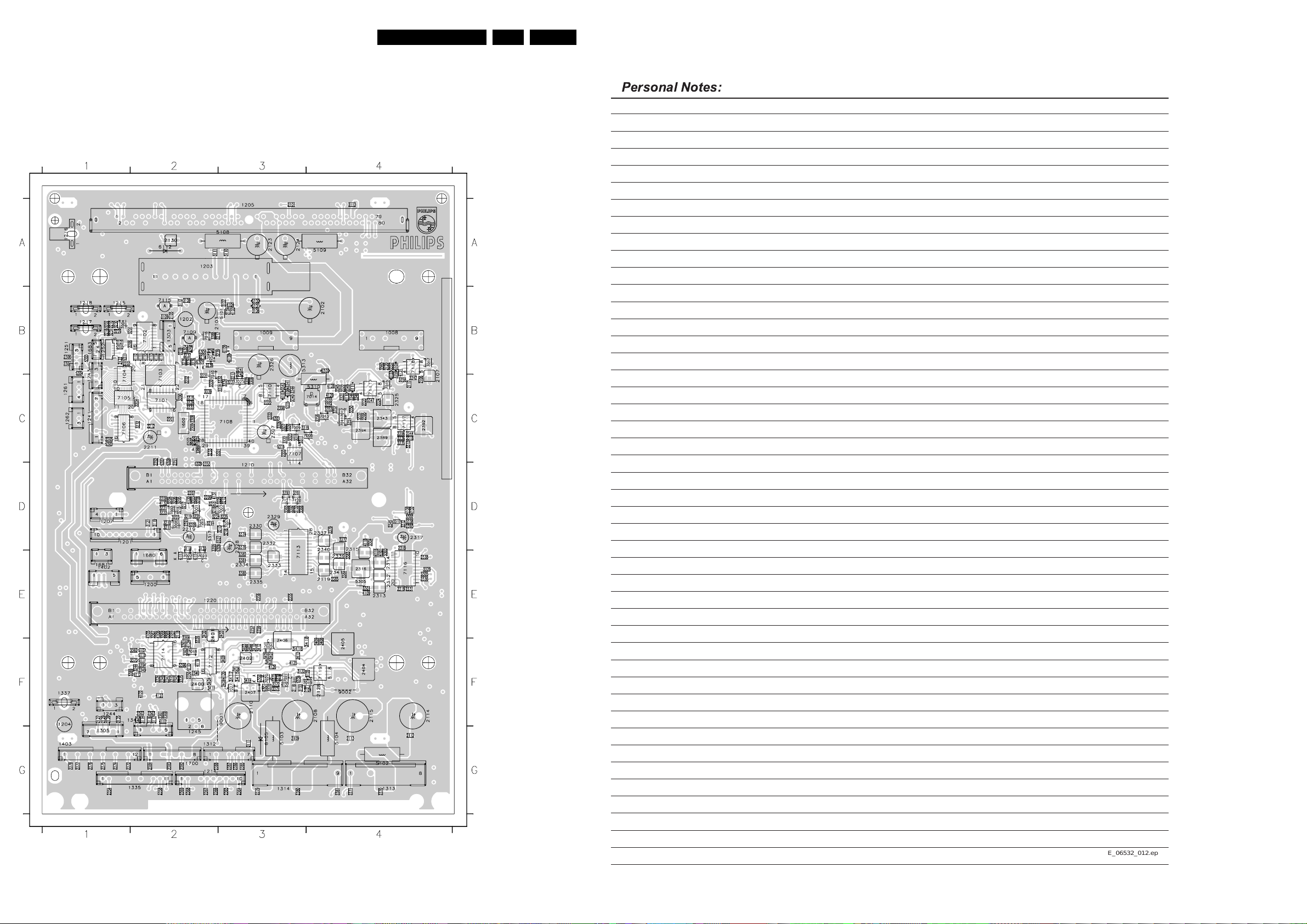
Circuit Diagrams and PWB Layouts
Layout LCoS System Board (Top Side)
2306 B1
2210 B1
2127 F1
2114 F4
2101 A3
1312 G2
1217 B1
1008 B4
1009 B3
1200 E2
1201 D1
1202 B2
1203 A2
1204 F1
1205 A3
1207 D1
1210 D3
1214 G2
1215 B1
1216 A1
1218 B1
1220 E2
1241 C1
1243 C1
1244 F1
1245 G2
1251 B1
1252 B1
1261 C1
1262 C1
1303 B2
1305 G1
1313 G4
1314 G3
1335 G2
1337 F1
1344 F2
1402 E1
1403 G1
1600 C2
1680 E2
1681 E1
1683 B1
1700 G2
3135 033 3299.6
2102 B4
2103 B2
2104 B3
2105 B2
2106 C4
2107 C4
2108 F4
2109 G3
2110 F3
2111 G3
2112 G4
2113 G4
2115 F4
2116 F3
2117 C4
2118 E2
2119 E4
2120 B4
2121 B1
2122 B1
2123 A3
2124 A3
2125 F1
2126 F1
2128 F4
2129 F1
2130 A2
2201 C2
2202 C2
2203 B1
2204 C2
2205 C1
2206 B1
2207 D2
2208 D2
2209 D2
2211 C2
2212 C2
2213 C3
2214 B2
2215 C2
2216 B1
2217 B2
2218 B2
2219 D2
2301 B1
2302 C3
2303 C3
2307 C3
2308 C2
2309 C2
2312 E4
2313 E4
2314 E4
2315 D4
2316 E4
2317 D4
2318 D4
2319 E4
2320 C3
2321 C4
2322 C4
2323 C4
2324 C4
2325 C4
2326 B3
2327 D3
2328 D3
2329 D3
2330 D3
2331 E4
2332 D3
2333 E3
2334 E3
2335 E3
2336 E4
2337 D4
2338 E4
2339 E4
2340 D4
2341 E4
2342 F2
2343 C4
2344 C4
2345 D4
2346 F2
2347 F2
2348 F2
2349 F2
2350 F2
2351 C2
2352 C2
2353 D2
2354 G1
2355 E3
2356 E3
2357 E3
2358 G2
2359 E3
2360 F2
2361 F2
2362 F2
2363 F2
2364 G3
2365 G3
2366 G2
2367 G2
2368 G2
2369 G2
2370 G4
2371 G4
2372 G1
2374 G1
2375 G1
2376 G1
2377 G1
2378 G1
2379 G3
2380 G3
2381 G4
2382 G2
2383 G2
2384 G2
2385 G3
2386 G3
2387 G3
2388 G2
2389 C4
2390 C3
2391 D2
2392 C4
2393 D4
2394 C4
2395 C4
2396 C4
2400 F2
2401 E2
2402 F3
2403 E3
2404 F4
2405 F4
2406 F3
2407 F3
2408 F3
2409 F4
3101 F3
3102 D3
3103 F3
3104 F4
3105 F4
3106 B3
E_14780_117.eps
3107 B3
3108 B2
3109 B2
3110 A3
3111 A2
3112 B2
3113 A4
3114 F2
3115 F2
3116 F2
3117 F2
3118 D2
3119 D2
130704
3120 D2
3121 D2
3122 F3
3201 B1
3202 B1
3203 D2
3204 D2
3205 D2
3206 D2
3207 D2
3208 D2
3209 D2
3210 D2
3211 D2
3212 D3
3213 D3
3214 D2
3215 D2
3216 D3
3217 D2
3218 D2
3219 D2
3220 D2
3221 D2
3222 D2
3223 D2
3224 D2
3225 D3
3226 D3
3227 C3
3228 C2
3229 B1
3230 B1
3231 B1
3232 C2
3233 C2
3234 B2
3235 B2
3236 B2
3237 B2
3238 B2
3239 B2
3240 B2
3241 B3
3242 C3
3243 B2
3244 F2
3301 E4
3302 D4
3303 E4
3304 D4
3305 E4
3306 C3
3307 C3
3308 C3
3309 C3
3310 F2
3311 C3
3312 D4
3313 C4
3314 C3
3315 C2
3316 C3
3317 D4
3318 C4
3319 C3
3320 C3
3321 C3
3322 C3
3323 C3
3324 F2
3325 F2
3326 F2
3328 C2
3329 E4
3330 C2
3331 C2
3332 C3
3333 C2
3334 C3
3335 C4
3336 C4
3337 C4
3338 D4
3339 C2
3340 C3
3341 C3
3342 C4
3343 C3
3344 C3
3345 C4
3346 C4
3347 C4
3348 C4
3349 C4
3350 C4
3351 C4
3352 C4
3353 C4
3354 C4
3355 C4
3356 C4
3357 B4
3358 C4
3359 C4
3360 B4
3361 F2
3362 F2
3363 F2
3364 E2
3365 D3
3366 D3
3367 E2
3368 E2
3369 E2
3370 F3
3371 F3
3372 F3
3373 F2
3374 D3
3375 F3
3376 D3
3377 D4
3378 F3
3379 D4
3380 E3
3381 E3
3382 E3
3383 E4
3384 E4
3385 E4
3388 B2
3389 F2
3390 C2
3391 D3
3392 D3
3393 D3
3394 F2
3395 D2
3396 F2
3400 E2
3401 F3
3402 F3
3403 F3
3404 F2
3405 F3
3406 F3
3407 F3
3408 F4
3409 F3
3410 F3
3411 F2
3412 F3
3413 F3
3414 F3
3415 F3
3416 F3
3417 F3
3418 F4
4101 E4
4102 D4
4103 B3
4104 B3
4105 E2
4106 E2
4107 E2
4108 D4
4109 E4
4110 B2
4111 B2
4112 B2
4113 B2
4114 B2
4115 B2
4116 E4
4117 F2
4118 D4
4119 F2
4120 F3
4121 B4
4122 F2
4123 F2
4124 F2
4125 F3
4126 F3
4127 F3
4128 C4
4129 C4
4130 D2
4131 D2
4132 D2
5101 B3
5102 G4
5103 G3
5104 G4
5106 F3
5107 F2
5108 A3
5109 A4
5110 F2
5111 F2
5112 F2
5113 F2
5301 C3
5302 C1
5303 B1
5304 B1
5305 E4
5306 D3
5307 C2
5308 C2
5309 D2
5310 C4
5311 B1
5312 B1
5313 B3
5315 C3
5316 C3
5317 D2
6101 B3
6102 B3
6103 C4
6104 B4
6105 G3
6106 C3
6107 C3
6108 B3
6109 B3
6110 C4
6111 C4
6112 A2
6113 E2
6114 E2
6201 C2
6202 C2
6300 F3
6301 F3
6302 B4
6304 B2
6305 B2
6306 B2
7001 D2
7002 D2
7003 D3
7004 B1
7005 D2
7006 D2
7007 D3
7008 C4
7009 C3
7010 C2
7011 C4
7012 C4
7013 C4
7014 C4
7015 C4
7016 B2
7017 B4
7018 F2
EN 28EM8E 7.
7019 F4
7020 F3
7021 F3
7022 E2
7023 E2
7024 B2
7025 C3
7026 F3
7027 F3
7101 C2
7102 B2
7103 C2
7104 C1
7105 C1
7106 C1
7107 C3
7108 C3
7109 B2
7110 C3
7111 C4
7112 F2
7113 E3
7114 F2
7115 B2
7116 E4
7117 C4
7118 B4
7119 F4
7120 D3
7121 D3
9001 F3
9002 F4
E_06532_012.eps
130204
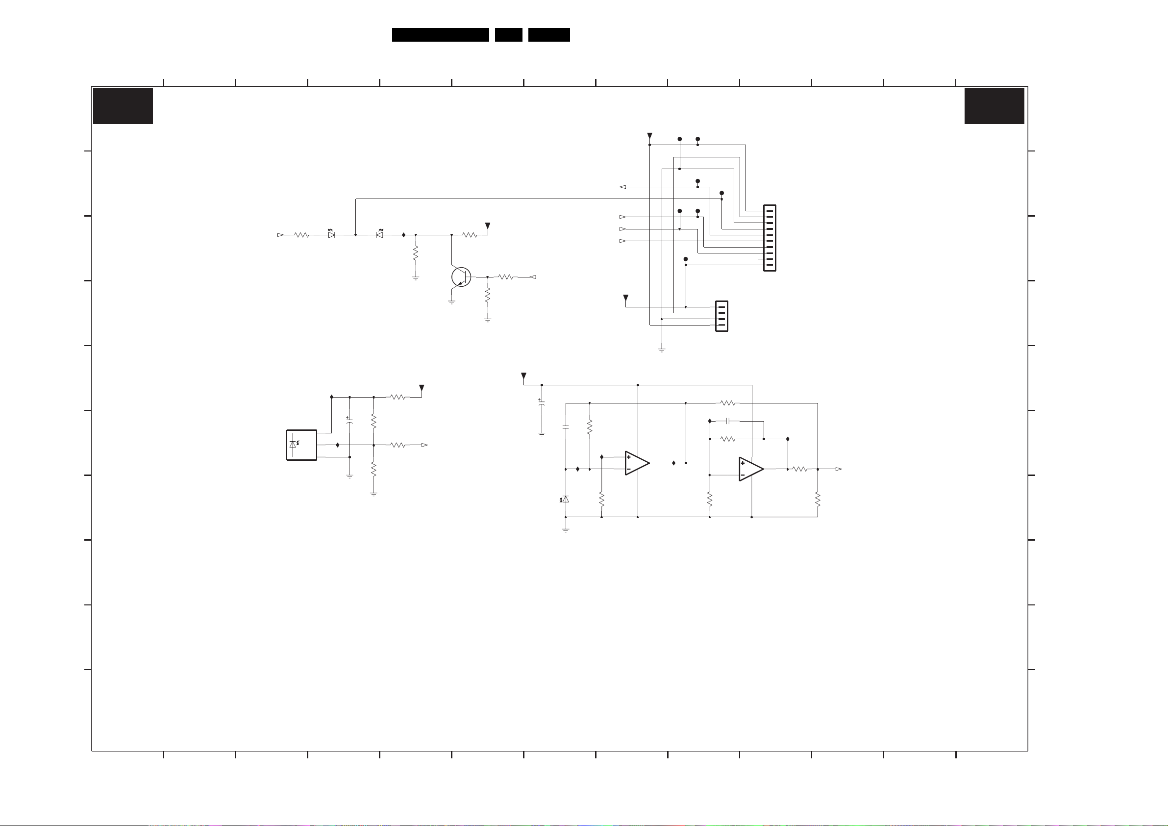
LED Sensor Panel
L S
L S
Circuit Diagrams and PWB Layouts
EN 29EM8E 7.
LS
A
B
C
D
E
F
G
21
3
LED SENSOR PANEL
ON_OFF_LED
1-B8
3001
150R
6003
VS
OUT
GND
TSOP2136UH1
6000-1
TLUV5300
ORANGE-RED
12
I012
2003
2
I013
1
3
10V100u
6000-2
TLUV5300
GREEN
6K8
3008
10K
3013
32
3006
330R
3002
470R
I011
+5V_STDBY
54
3007
1-B8
1K5
BC847B
RC5
7001
3003
1K2
6
+9V
3004
10K
3005
15K
+9V
1-C8
STANDBY
50V10u
2001
7
2002
6004
ON_OFF_LED
LIGHT_SENSOR
STANDBY
470n
3009
I015
BPW46
1M5
I016
3014
RC5
1M5
1-C3
1-F5
1-F11
1-C7
+9V
+5V_STDBY
8
7000-1
LM358DR2
4
F001
F004
I017
F006
F002
F003
F005
1201
S4B-EH
I020
3016
F007
1
+9V
2
KEYBOARD
3
GND KEYBOARD
4
+5V_STDBY
3010
10K
2004
470n
3011
3K3
1K0
1214
S10B-EH
8
7000-2
LM358DR2
4
+5V STANDBY
1
KEYBOARD
2
SGND
3
LAMP FAULT
4
ON/OFF LED
5
STANDBY
6
RC5
7
LIGHT SENSOR
8
9
+9V
10
I019
3012
4K7
3017
1-C8
3K3
111098
LIGHT_SENSOR
1312
LS
A
B
C
D
E
F
G
1201 D9
1214 B10
2001 E7
2002 F7
2003 F4
2004 F9
3001 C3
3002 F5
3003 C6
3004 D6
3005 C6
3006 E5
3007 C5
3008 F4
3009 F7
3010 E9
3011 F9
3012 F10
3013 F4
3014 G8
3015 G9
3016 G9
3017 G11
6000-1 C4
6000-2 C4
6003 F3
6004 G7
7000-1 F8
7000-2 F10
7001 C6
F001 A9
F002 A9
F003 B9
F004 B9
F005 B9
F006 C9
F007 B9
I011 C5
I012 E4
I013 F4
I015 F7
I016 F8
I017 F9
I019 F10
I020 F9
H
I
J
3135 033 3315.4
1
NOTES
1. CAPACITANCE VALUES ARE IN FARADS:
m=MILI u=MICRO n=NANO p=PICO f=FEMTO
2. RESISTANCE VALUES ARE IN OHMS:
R=OHM K=KILO M=MEGA G=GIGA T=TERA
3. SAFETY TRIANGLE REPRESENTS PCEC REPLACEMENT PART ONLY.
4. FOR VALUE SEE TABLE.
*
5432
H
I
J
E_14780_096.eps
130704
6
7
98
1110
12
13
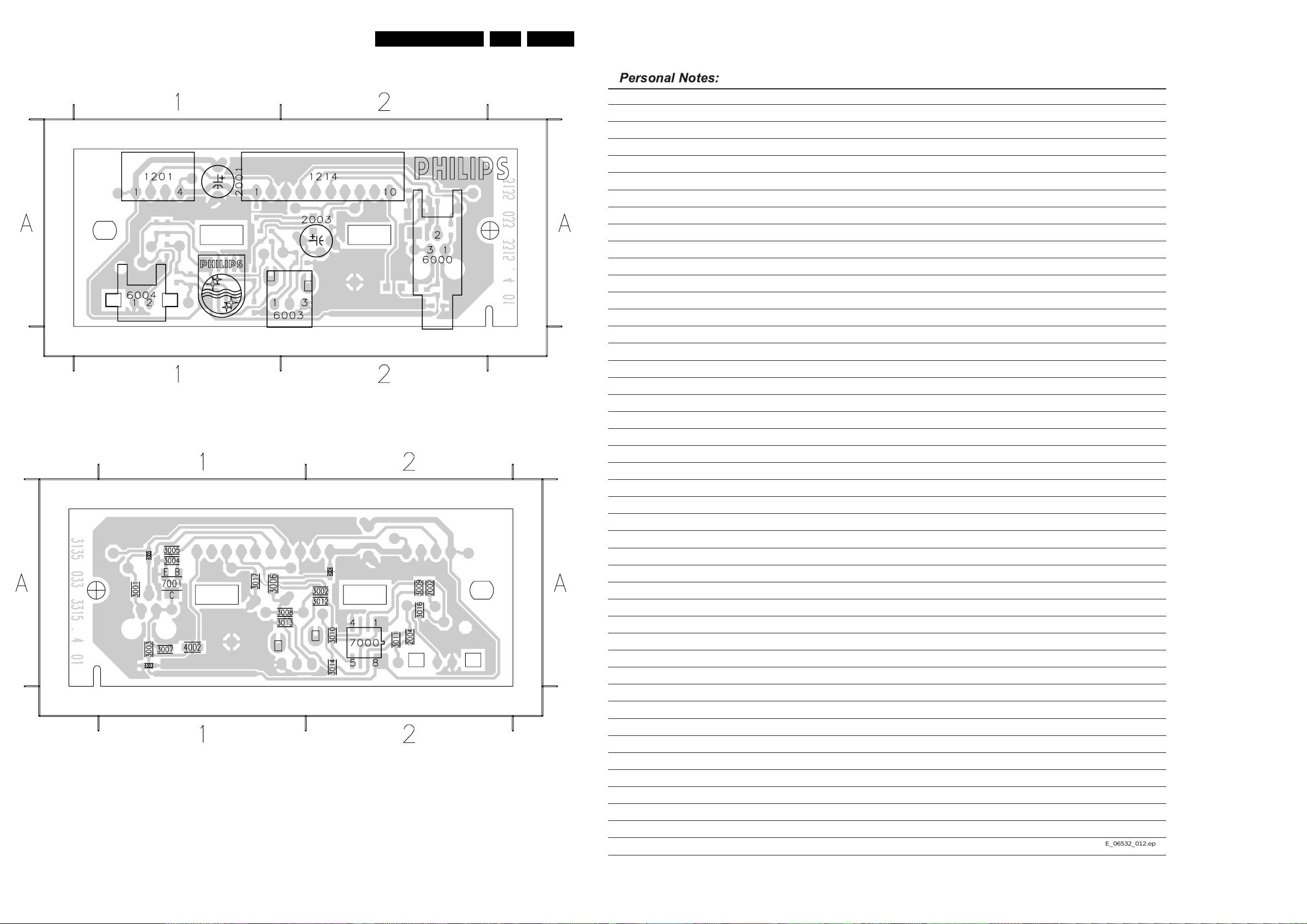
Circuit Diagrams and PWB Layouts
Layout LED Sensor Panel (Top Side)
1201 A1 1214 A2 2001 A1 2003 A2 6000 A2 6003 A2 6004 A1
EN 30EM8E 7.
3135 033 3315.4
Layout LED Sensor Panel (Bottom Side)
2002 A2
2004 A2
3001 A1
3002 A2
3003 A1
3004 A1
3005 A1
3006 A1
3007 A1
3008 A1
3009 A2
3010 A2
3011 A2
3012 A2
3013 A1
3014 A2
3016 A2
3017 A1
4002 A1
4003 A1
4004 A2
4005 A1
7000 A2
7001 A1
E_14780_098 .eps
130704
3135 033 3315.4
E_14780_099 .eps
130704
E_06532_012.eps
130204
 Loading...