

Page 1

PHILIPS SERVICE AND QUALITY/TRAINING
LCOS
LIQUID CRYSTAL ON SILICON
EM7U LCOS REAR PROJECTION TV
PHILIPS
TECH
VIDEOTAPE S
MANUALS
PHILIPS SERVICE AND QUALITY/TRAINING
ONE PHILIPS DRIVE
PO BOX 14810
KNOXVILLE, TN 37914-1810
PHONE: 865-521-4397
FAX: 865-521-4818
TRAINING
EMAIL: TECHNICAL.TRAINING@PHILIPS.COM
Page 2

Page 3

Table of Contents
Introduction . . . . . . . . . . . . . . . . . . . . . . . . . . . . . . . . . . . . . . . . . . . . . . . . . . . . . . . . . .1
Set Operation . . . . . . . . . . . . . . . . . . . . . . . . . . . . . . . . . . . . . . . . . . . . . . . . . . . . . . . .2
Remote Control . . . . . . . . . . . . . . . . . . . . . . . . . . . . . . . . . . . . . . . . . . . . . . . . . . . . . . .3
Picture Formats . . . . . . . . . . . . . . . . . . . . . . . . . . . . . . . . . . . . . . . . . . . . . . . . . . . . . . .4
Reflective LCD Projection System . . . . . . . . . . . . . . . . . . . . . . . . . . . . . . . . . . . . . . . . .6
Power Supply Block . . . . . . . . . . . . . . . . . . . . . . . . . . . . . . . . . . . . . . . . . . . . . . . . . . .8
AC Input . . . . . . . . . . . . . . . . . . . . . . . . . . . . . . . . . . . . . . . . . . . . . . . . . . . . . . . . . . . .8
Standby Supply . . . . . . . . . . . . . . . . . . . . . . . . . . . . . . . . . . . . . . . . . . . . . . . . . . . . . . .12
Main Power Supply . . . . . . . . . . . . . . . . . . . . . . . . . . . . . . . . . . . . . . . . . . . . . . . . . . . .14
3.3 Volt Regulator . . . . . . . . . . . . . . . . . . . . . . . . . . . . . . . . . . . . . . . . . . . . . . . . . . . . .16
Audio Power Supply . . . . . . . . . . . . . . . . . . . . . . . . . . . . . . . . . . . . . . . . . . . . . . . . . . .18
Lamp Supply . . . . . . . . . . . . . . . . . . . . . . . . . . . . . . . . . . . . . . . . . . . . . . . . . . . . . . . . .20
Video Signal Flow Block . . . . . . . . . . . . . . . . . . . . . . . . . . . . . . . . . . . . . . . . . . . . . . . .22
Overall Block 1FH Section . . . . . . . . . . . . . . . . . . . . . . . . . . . . . . . . . . . . . . . . . . . . . . .23
Side Jack Panel . . . . . . . . . . . . . . . . . . . . . . . . . . . . . . . . . . . . . . . . . . . . . . . . . . . . . .25
AV1 Input . . . . . . . . . . . . . . . . . . . . . . . . . . . . . . . . . . . . . . . . . . . . . . . . . . . . . . . . . . .26
1H Component Input . . . . . . . . . . . . . . . . . . . . . . . . . . . . . . . . . . . . . . . . . . . . . . . . . . .27
1FH Jack Panel Switching . . . . . . . . . . . . . . . . . . . . . . . . . . . . . . . . . . . . . . . . . . . . . . .28
Main Tuner . . . . . . . . . . . . . . . . . . . . . . . . . . . . . . . . . . . . . . . . . . . . . . . . . . . . . . . . . .29
HIP (High-end Input Processor) Circuit . . . . . . . . . . . . . . . . . . . . . . . . . . . . . . . . . . . . .30
NTSC Comb Filter Circuit . . . . . . . . . . . . . . . . . . . . . . . . . . . . . . . . . . . . . . . . . . . . . . .32
PIP/Double Window Input . . . . . . . . . . . . . . . . . . . . . . . . . . . . . . . . . . . . . . . . . . . . . . .34
Double Window PIP Output . . . . . . . . . . . . . . . . . . . . . . . . . . . . . . . . . . . . . . . . . . . . . .34
Double Window Control and Power Supply . . . . . . . . . . . . . . . . . . . . . . . . . . . . . . . . . .34
Feature Box . . . . . . . . . . . . . . . . . . . . . . . . . . . . . . . . . . . . . . . . . . . . . . . . . . . . . . . . .38
Eagle . . . . . . . . . . . . . . . . . . . . . . . . . . . . . . . . . . . . . . . . . . . . . . . . . . . . . . . . . . . . . .40
LVDS Transmitter . . . . . . . . . . . . . . . . . . . . . . . . . . . . . . . . . . . . . . . . . . . . . . . . . . . . .42
2H Section Block . . . . . . . . . . . . . . . . . . . . . . . . . . . . . . . . . . . . . . . . . . . . . . . . . . . . . .43
AV3 and AV4 Inputs . . . . . . . . . . . . . . . . . . . . . . . . . . . . . . . . . . . . . . . . . . . . . . . . . . .47
Analog Input A/D Conversion . . . . . . . . . . . . . . . . . . . . . . . . . . . . . . . . . . . . . . . . . . . . .49
Reference Voltage and A/D Converters . . . . . . . . . . . . . . . . . . . . . . . . . . . . . . . . . . . . .59
Input Latch and PLD Sync . . . . . . . . . . . . . . . . . . . . . . . . . . . . . . . . . . . . . . . . . . . . . . .59
ADC Clock Circuit . . . . . . . . . . . . . . . . . . . . . . . . . . . . . . . . . . . . . . . . . . . . . . . . . . . . .59
Light Engine Block . . . . . . . . . . . . . . . . . . . . . . . . . . . . . . . . . . . . . . . . . . . . . . . . . . . . .63
Audio Signal Delay . . . . . . . . . . . . . . . . . . . . . . . . . . . . . . . . . . . . . . . . . . . . . . . . . . . .71
Audio Power Amplifier . . . . . . . . . . . . . . . . . . . . . . . . . . . . . . . . . . . . . . . . . . . . . . . . . .74
Audio Protection Circuit . . . . . . . . . . . . . . . . . . . . . . . . . . . . . . . . . . . . . . . . . . . . . . . . .76
Center Channel Switch . . . . . . . . . . . . . . . . . . . . . . . . . . . . . . . . . . . . . . . . . . . . . . . . .76
Headphone Switch and Amplifier . . . . . . . . . . . . . . . . . . . . . . . . . . . . . . . . . . . . . . . . . .78
OTC Communication . . . . . . . . . . . . . . . . . . . . . . . . . . . . . . . . . . . . . . . . . . . . . . . . . . .80
Light Sensor . . . . . . . . . . . . . . . . . . . . . . . . . . . . . . . . . . . . . . . . . . . . . . . . . . . . . . . . .82
Keyboard . . . . . . . . . . . . . . . . . . . . . . . . . . . . . . . . . . . . . . . . . . . . . . . . . . . . . . . . . . .82
2
I
C Interconnect - Part One . . . . . . . . . . . . . . . . . . . . . . . . . . . . . . . . . . . . . . . . . . . . . .83
LED Circuit . . . . . . . . . . . . . . . . . . . . . . . . . . . . . . . . . . . . . . . . . . . . . . . . . . . . . . . . . .83
2
I
C Interconnect - Part Two . . . . . . . . . . . . . . . . . . . . . . . . . . . . . . . . . . . . . . . . . . . . . .85
2
I
C Interconnect - Part Three . . . . . . . . . . . . . . . . . . . . . . . . . . . . . . . . . . . . . . . . . . . . .85
Fan Drive Circuit . . . . . . . . . . . . . . . . . . . . . . . . . . . . . . . . . . . . . . . . . . . . . . . . . . . . . .87
Wiring Interconnect . . . . . . . . . . . . . . . . . . . . . . . . . . . . . . . . . . . . . . . . . . . . . . . . . . . .91
Disassembly . . . . . . . . . . . . . . . . . . . . . . . . . . . . . . . . . . . . . . . . . . . . . . . . . . . . . . . . .94
Page 4
INTRODUCTION
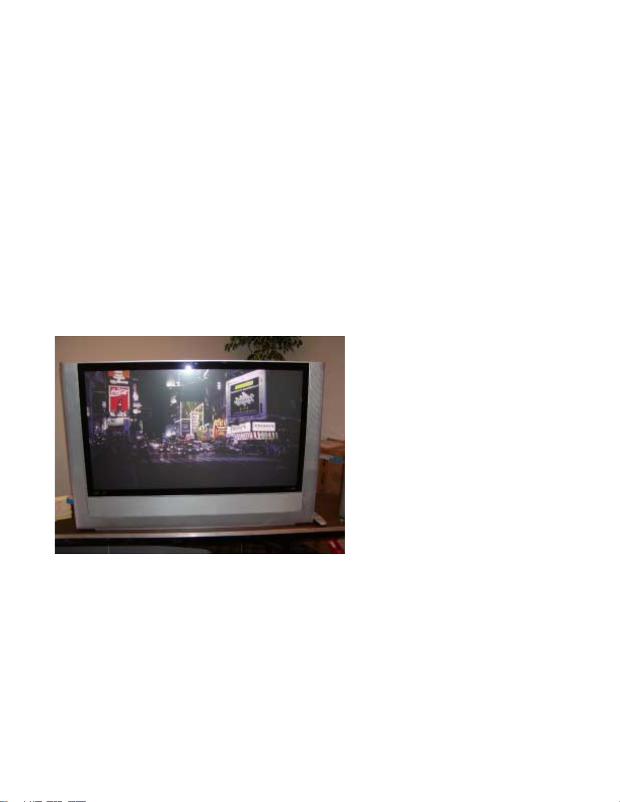
The EM7U chassis is designated for release in the 2003 model year. This is a rear projector
based on LCOS (Liquid Crystal on Silicon) technology. LCOS is a reflective LCD technology.
The light source is an ARC projection lamp that is replaceable by the customer. This projector is lighter and more compact that comparable size projection sets using tubes. They will
be available in 44 and 55 inch screen sizes. All of the screen sizes will have a 16x9 aspect
ratio. The following table shows the dimensions and weights.
Screen size Height Width Depth Weight
44 inch 31.7" 46.7" 14.6" 68.8 lbs
55 inch 38.7" 57" 17.7" 83.9lbs
The EM7U will come in the Epic and Matchline formats. The Matchline version will have
Pixel Plus for the 1H inputs. The EM7U is a High Definition Ready set with a screen resolution of 1280x720. It does not have a ATSC Tuner built in. A Set Top box will be required for
viewing ATSC signals.
44 INCH LCOS PROJECTOR
INPUTS
2 1FH INPUTS
1 COMPONENT
3 SVHS
3 COMPOSITE
4 2FH INPUTS
2 COMPONENT
1 RGB
1 DVI
Page 1
Page 5
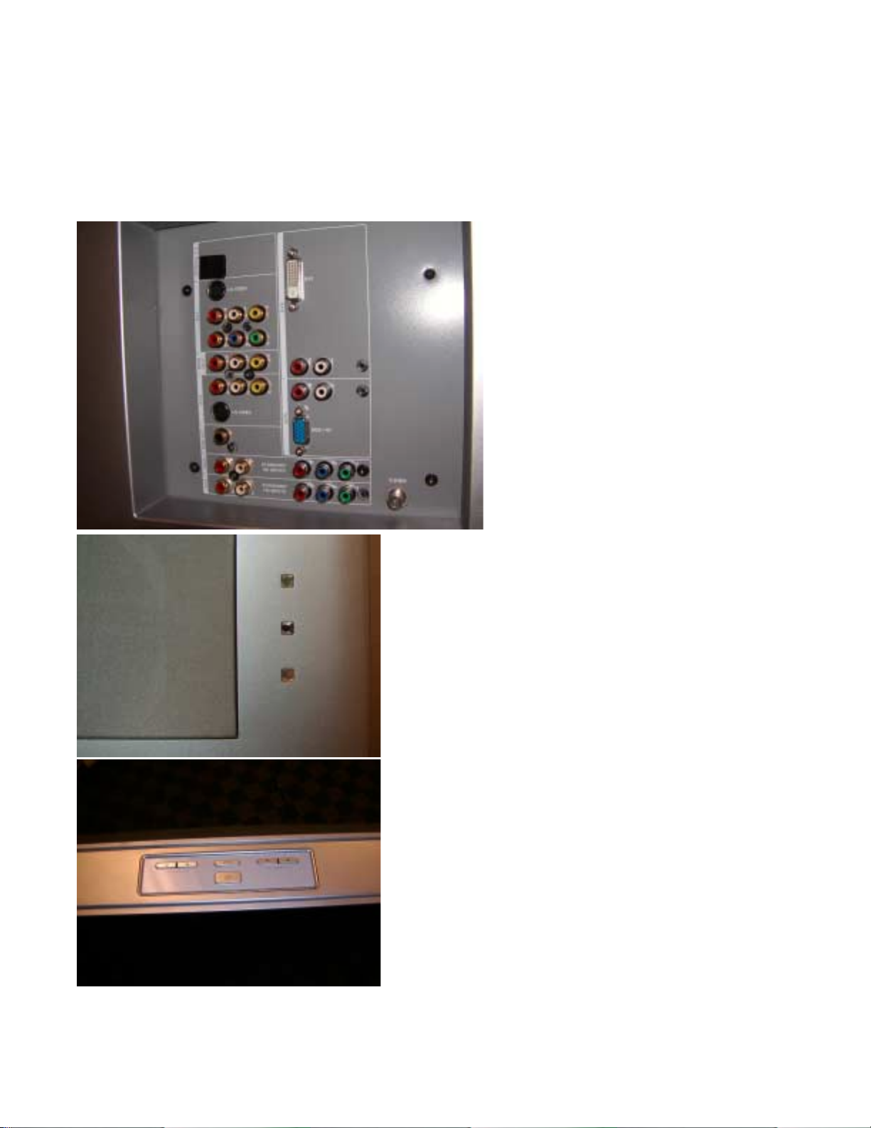
SET OPERATION
The set has three 1H or NTSC only inputs. They are AV1 and AV2 located on the rear Jack
Panel. The third input is the Side Jack panel. AV3 and AV4 can be either 1H NTSC, 480P,
or 1080I signals. These signals must be in the Y Pb Pr format. AV5 is a DB15 RBG input.
AV6 is a DVI 1080I input connector. The RF input on the Rear Jack panel is for NTSC only.
The MON OUT is a monitor output for whichever 1H Tuner, AV1, AV2, or Side Jack panel
signal has been selected.
REAR JACK PANEL
The indicator LEDs and the Remote Control
Receiver are located on the front of the set. When
the set is turned On, the Amber LED will turn On.
After the Lamp in the set has switched On, the
Green LED will turn On.
The Control Panel is located at the top of the set.
The Power On button is lighted with a blue LED
whenever power is applied to the set.
Page 2
Page 6
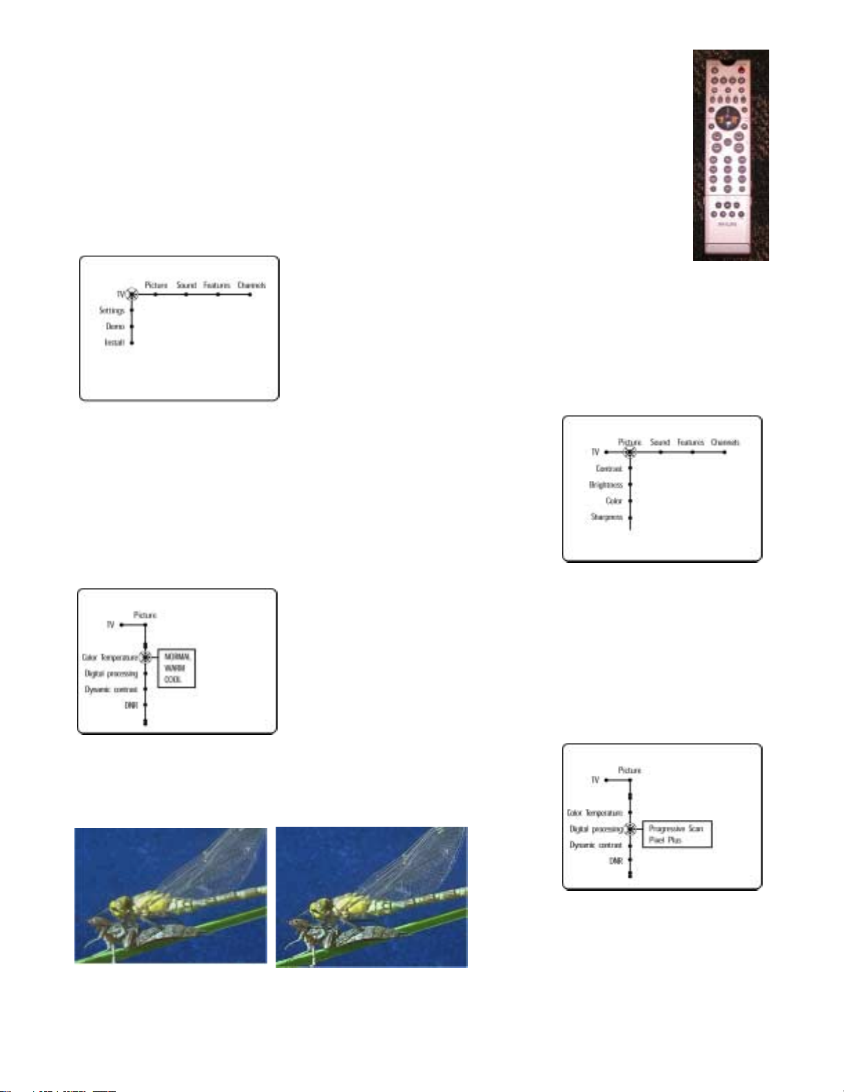
Remote Control Figure 1
When the set is turned On via the Keyboard or Remote Control, the set will take
approximately 30 seconds to display a picture. By using the Select button, the
Remote can be used to control other devices. A list of setup codes for other
devices is located in the customer's operator’s manual. The customer can select
the Menu button on the Remote to make additional selections and adjustments as
desired. Use the cursor right and cursor down buttons on the Remote to select the
desired topic.
When Picture is selected, use the cursor down
button to select the desired subtopic. For example, press the
cursor down button to select Contrast then use the cursor left
and cursor right buttons to change the values. Additional dots
on the lower part of the line indicate that additional selections
are present. Continue to press the cursor down button to make
these selections.
FIGURE 1 - MAIN MENU
desired subtopic. (Figure 2) For example, press the cursor
down button to select Contrast then use the cursor left and cursor right buttons to change the values. Additional dots on the
lower part of the line indicate that additional selections are present. Continue to press the cursor down button to make these
selections.
FIGURE 3 - COLOR
TEMPERATURE
(Figure 4) Pixel Plus provides additional picture enhancement.
When Picture is selected, use the
cursor down button to select the
Under Color Temperature, there are
three selections: Normal, Warm,
and Cool. (Figure 3) With the Normal selection, the picture displays a normal Gray Scale. If the customer desires a reddish tint
to the picture, Warm is selected. Cool shifts the picture's gray
scale in the direction of Blue.
With sets with Pixel Plus, the C
customer can select between
Progressive Scan and Pixel Plus.
FIGURE 2 - PICTURE
SELECTION
Pictures with Pixel Plus Off (left) and On (right).
Page 3
FIGURE 4 - PIXEL
PLUS SELECTION
Page 7
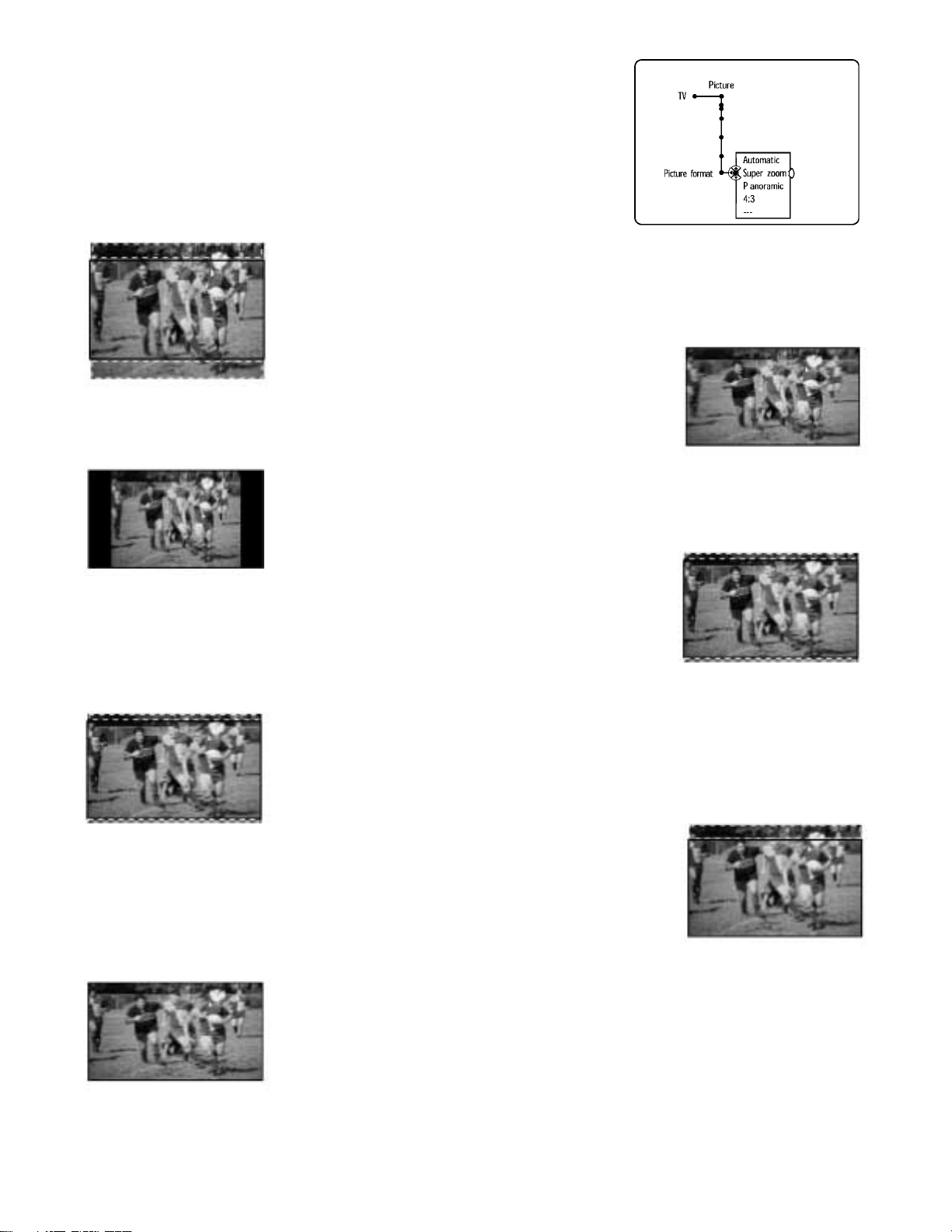
Picture Formats
There are seven different Picture Formats: Super Zoom,
Panoramic, 4:3, Movie Expand 14:9, Movie expand 16:9, 16:9
Subtitle, or Wide screen, which can be selected by the customer. (Figure 5) When portions of the picture are deleted, the
cursor buttons on the Remote can shift the picture to select the
area to be deleted.
Super Zoom enlarges the picture vertically
without distortion. (Figure 6) Some of the top and bottom portions of
the picture will be deleted.
FIGURE 5 - PICTURE
FORMATS
FIGURE 6 - SUPER
ZOOM
linear to display a 4:3 picture on a 16:9 screen. (Figure 7)
FIGURE 8 - 4x3
MODE
portions of the picture will be deleted. Black or gray bars will show at
the left and right sides. (Figure 9) This would be used by the viewer if
the original material was in the 14x9 letterbox format.
FIGURE 10 - 16x9
EXPAND FORMAT
played at the bottom of the screen. (Figure 11) The top portion of the
picture will be deleted in this mode. This Format digitally stretches the
picture vertically, then shifts it up.
The Panoramic format evenly stretches the
edges while keeping the center of the picture
The 4x3 Format displays a 4:3 picture without
change. Black or gray bars will show at the left
and right sides. (Figure 8) There is no loss of picture on the top and
bottom.
Movie Expand 14:9 displays the picture in a
14:9 aspect ratio. Some of the top and bottom
Movie Expand 16:9 format stretches the picture
horizontally and vertically to fill the 16:9 screen. Some of the top and
bottom portions of the picture will be deleted. (Figure 10) This Format
would be used by the viewer if the original material was in the 16x9
letterbox format.
The 16:9 Subtitle format zooms the picture for a
full view of subtitles or other information dis-
FIGURE 7 -
PANORAMIC MODE
FIGURE 9 - 14x9
EXPAND FORMAT
FIGURE 11 - 16x9
SUBTITLE FORMAT
FIGURE 12 - WIDE
SCREEN FORMAT
The Wide Screen format evenly stretches the width of a 4:3 picture to
fill the screen. (Figure 12) The viewer would use this Format if the
original material was in a 16x9 compressed Format.
Page 4
Page 8
Under the Channels title, is the channel guide lock selection.
(Figure 13) The customer can lock out selected channels or
channels that are transmitting a selected rating code. These
channels can only be view when the code selected by the customer is entered. If the customer forgets the code, a code of
0711 entered twice can be used to unlock the set.
A dust filter
is located
under the
Power Cord
to prevent dust buildup in the set. (Figure
14) This is an item that can be replaced
by the customer. Under certain
conditions, if this filter becomes dirty, the
set could overheat and shut down.
FIGURE 13 - CHANNEL
LOCKING
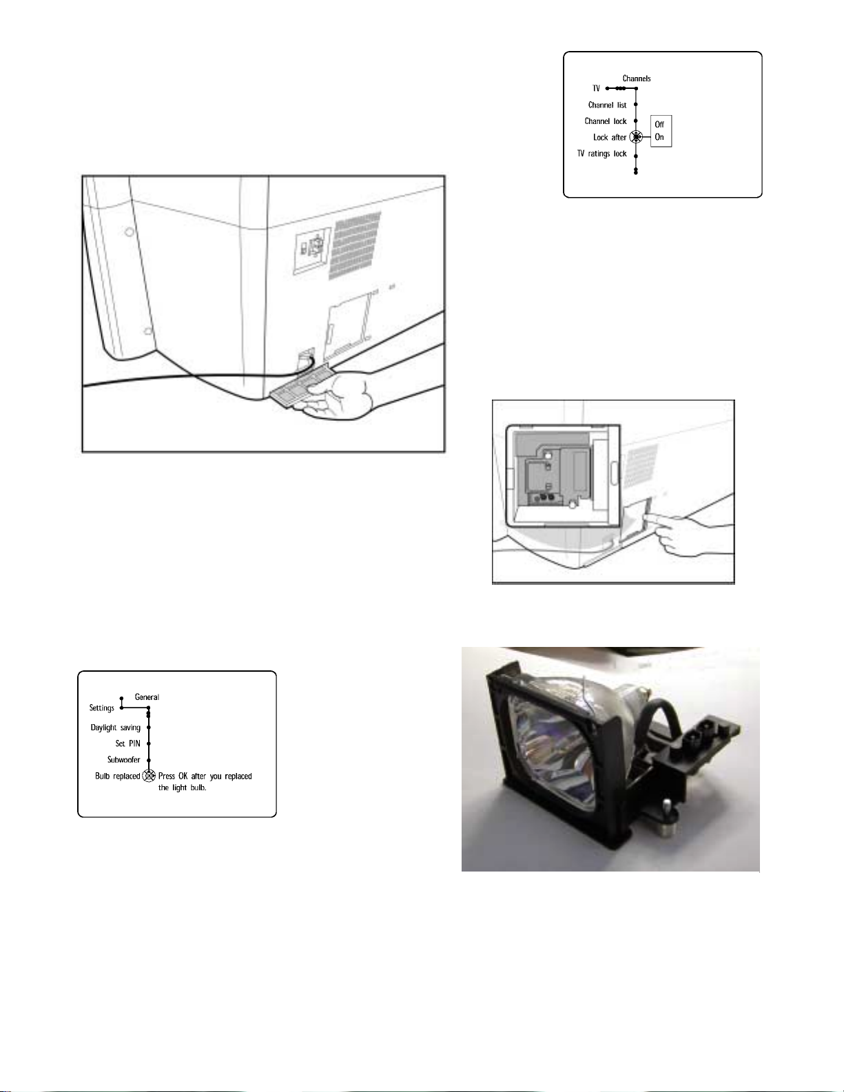
FIGURE 14 - DUST FILTER REMOVAL
The projection lamp is replaceable by the customer.
(Figure 15) A door near the Power Cord allows
access to the Lamp. When this door is open, an
interlock switch will prevent the set from being
turned On. When the back cover is removed, the
switched is in the closed position allowing the set to
be serviced.
A timer in the set will
inform the customer
when the Lamp should
be changed. Under
the Settings/General
title, the Bulb Replaced
selection will reset the
FIGURE 16 - LAMP
TIMER RESET
The Timer is set for 6000 hours.
timer when the OK button on the Remote is
pressed. (Figure 16)
FIGURE 15 - PROJECTION
LAMP REPLACEMENT
REPLACEMENT PROJECTION LAMP
When the set is turned On, it takes approximately 30 seconds before the lamp will turn On.
There is an approximate 30 second shutdown time before the set turns Off and can be turned
On again.
Page 5
Page 9
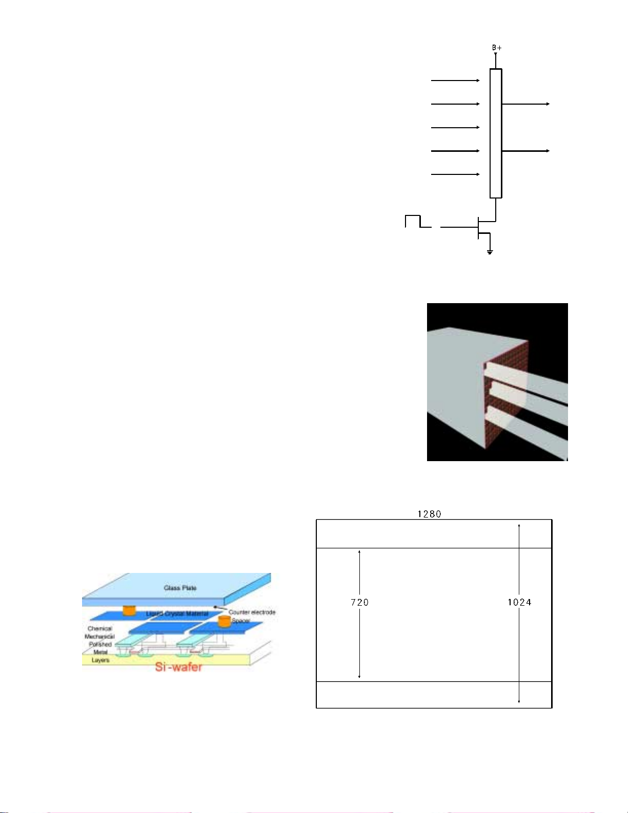
REFLECTIVE LCD PROJECTION SYSTEM
The LCOS (Liquid Crystal on Silicon) uses a reflective LCD
system. A single reflective LCD panel with multiple LCD
cells is used. Since a single panel is used, it is necessary
to scan the panel with the primary colors to obtain a color
picture. A LCD is a light valve which allows more or less
light through it, depending on the applied voltage. See
Figure 17.
The LCD used in most projectors and direct view LCD TVs
uses a transmissive type of LCD. (Figure 18) Light is projected to pass through the LCD panel. One of the disadvantages of this type of system is that the electronics to
control the LCD cells limit the surface area in which light
can pass. This limits the resolution of the picture and
brightness.
The Reflective type of LCD, like the one used in the LCOS, has
the electronics beneath the LCD cells, allowing greater resolution.
(Figure 19) The LCD cells are turned On, switching the individual
cells. Beneath each cell is a reflective surface. The amount of
light reflected from each cell depends on the applied voltage.
Since the LCD may be illuminated by all three primary colors at
one time, several cells are addressed at once.
FIGURE 17 - LCD CELL
The Reflective LCD used in the LCOS projector uses a 1280x1024
device with 20 micron pixels. Since the aspect ratio of the TV is
16x9, the actual area used is 1280x720. (Figure 20)
Regardless of the format of the input, the LCD displays the picture
in a 1280x720 format.
FIGURE 20 - LCD SURFACE AREA
FIGURE 19 - REFLECTIVE LCD
FIGURE 18 -
TRANSMISSIVE LCD
Page 6
Page 10
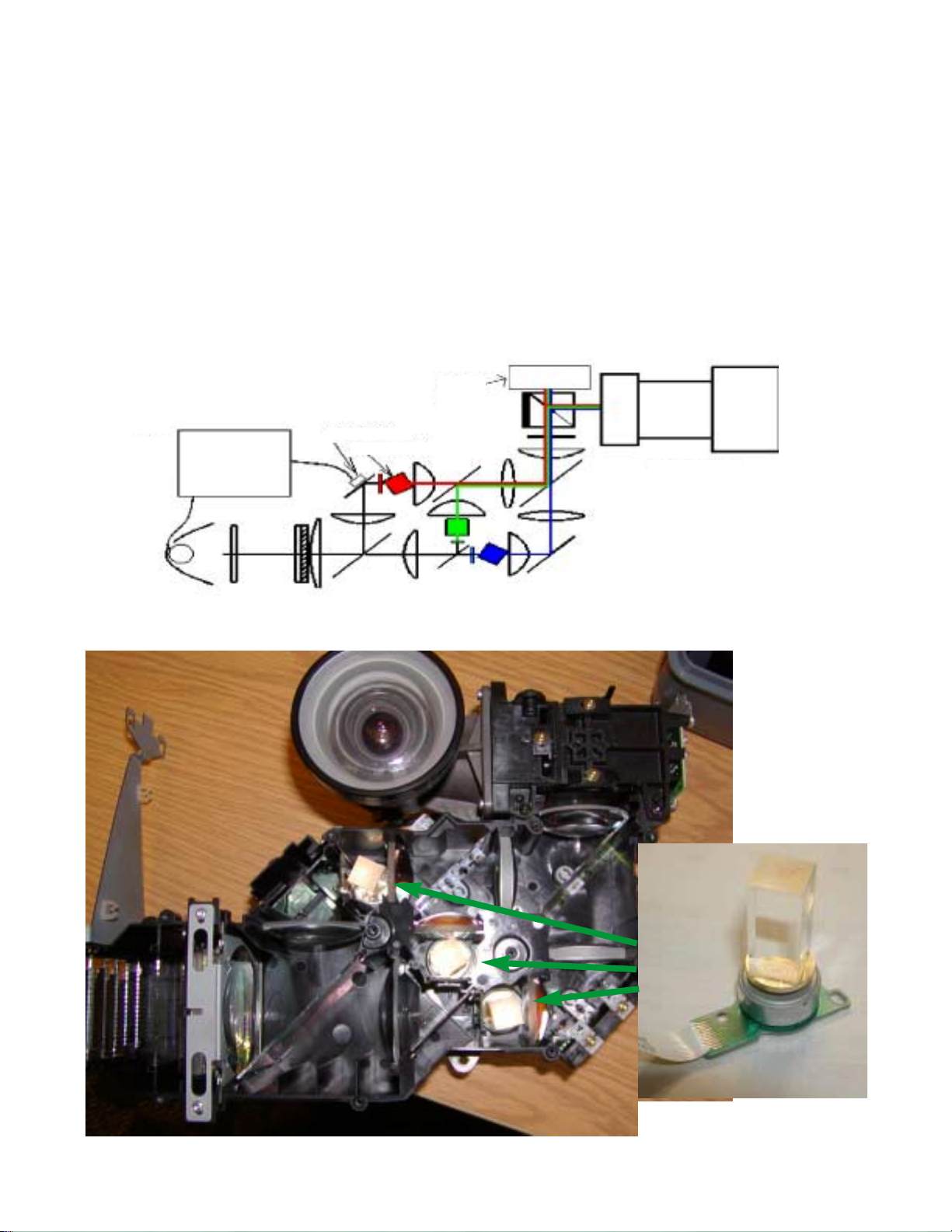
The Philips LCOS projector uses a single LCD device. To obtain a color picture, the LCD is
scanned with strips of Red, Green, and Blue light. The strips of color are developed by splitting the light from the Lamp and directing it to three color filters which produce Red, Green,
and Blue light. The output from the filters is directed to three rotating Prisms to produce the
color strips and direct it to the correct part of the LCD. Data is directed to the LCD in such a
way that the correct data for color illuminating that portion of the LCD will be displayed. The
LCD is being scanned a rate of 180 Hz. The phase of each prism is offset by 30 degrees to
provide color separation. The reflected light from the LCD is fed to a projection lens, the mirror, and finally the screen.
LIQUID
CRYSTAL
DISPLAY
LAMP
DRIVER
LAMP
LIGHT SENSOR
SCANNING PRISM
PROJECTION LENS
LIGHT ENGINE LIGHT PATH
Page 7
PRISM
LIGHT ENGINE WITHOUT LAMP AND PC BOARD
Page 11

POWER SUPPLY BLOCK (Figure 21)
The Bridge Rectifiers, On/Off Relay, Audio Power supply, and Lamp supply are located on the
Power Input board. The Standby and Main supplies are located on the Main Power board.
AC is applied to the Power Input Board via connector 1212. This voltage is rectified to produce the RAWDC-STBY and is fed to the Main Power Board. This feeds the Standby Supply
that produces a +5V2 supply. This supply feeds the Power Relay on the Power Input board
and the SSB to power the Microprocessor.
The AC input voltage is also fed to a Switch controlled by the Microprocessor on the SSB via
the System Board. When the set is turned On, the Standby line goes Low, switching the
Relay On. This is fed to a rectifier that supplies RAW_DC to the Audio Supply and Lamp
Supply located on the Power Input Board. The rectifier is connected as a voltage doubler. It
also supplies RAW_DC to the Main Supply located on the Main Power Board. The Audio
Supply provides a positive and negative voltage to the Audio Amplifier Board. The Lamp
Supply is a Boost regulator that supplies 330 volts to the Lamp Driver board.
The Main Supply produces a +36, a +12, a +22 and a +9 volt supply. The +9 volt supply is
also fed to a 3.3 volt regulator.
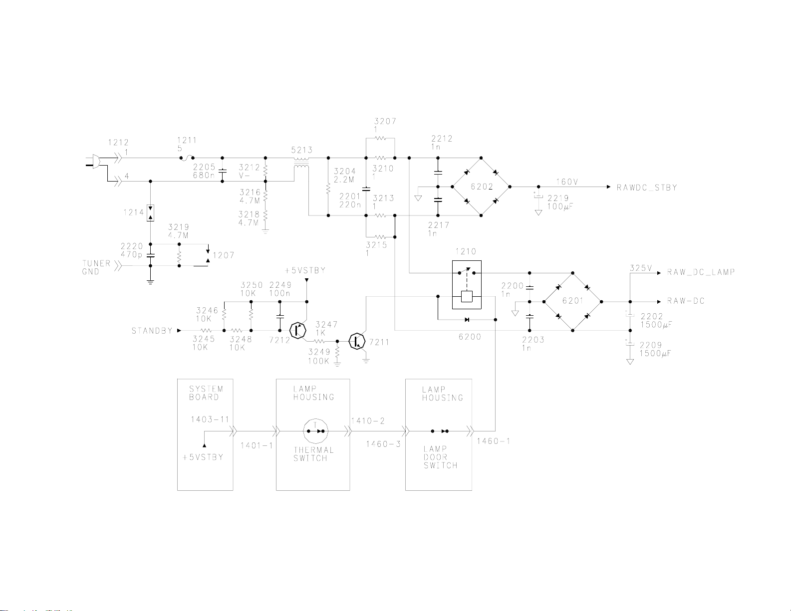
AC INPUT (Figure 22)
AC power is connected to the Power Input board via connector 1212. Fuse 1211 provides
protection against overcurrent. Spark gaps 1214 and 1216 provide protection against excessive voltage spikes on the AC line. Resistors 3207, 3210, 3213, and 3215 limit the current
when power is first applied to the set. Bridge 6202 rectifies the AC voltage to produce the
RAWDC_STBY for the Standby regulator.
Bridge 6201 provides power for the Lamp Supply and the Main Power supply. When the set
is turned On, Relay 1210 switches On to provide power to 6201. Bridge 6201, Capacitors
2202 and 2209 constitute a voltage doubler circuit. When the set is turned On, the Standby
line goes Low. Transistor 7212 turns On turning transistor 7211 On, switching the Relay 7210
On. The ground side of the Relay is connected to the Lamp Door Interlock switch and the
Thermal switch which is located on the Lamp Housing. If the Projection Lamp Door is open
or the Lamp Housing has overheated, the set cannot be turned On.
Page 8
Page 12
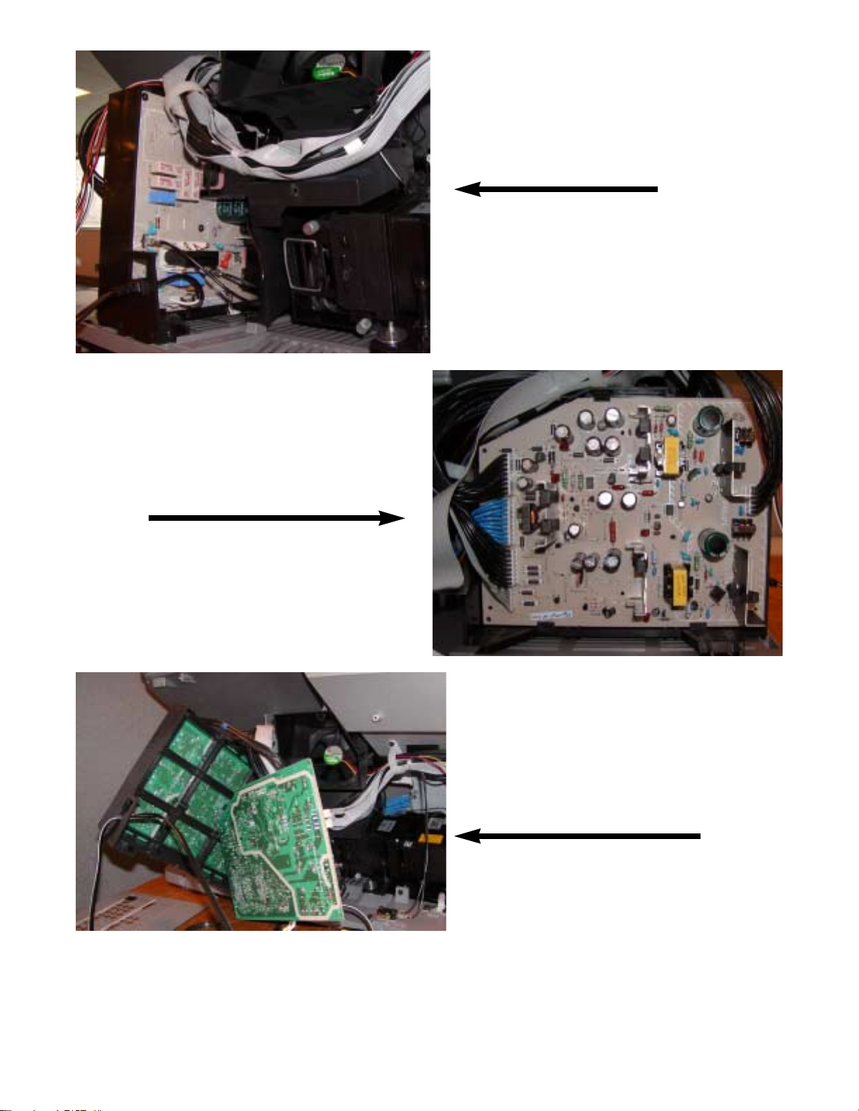
MAIN POWER BOARD
POWER INPUT BOARD
Page 9
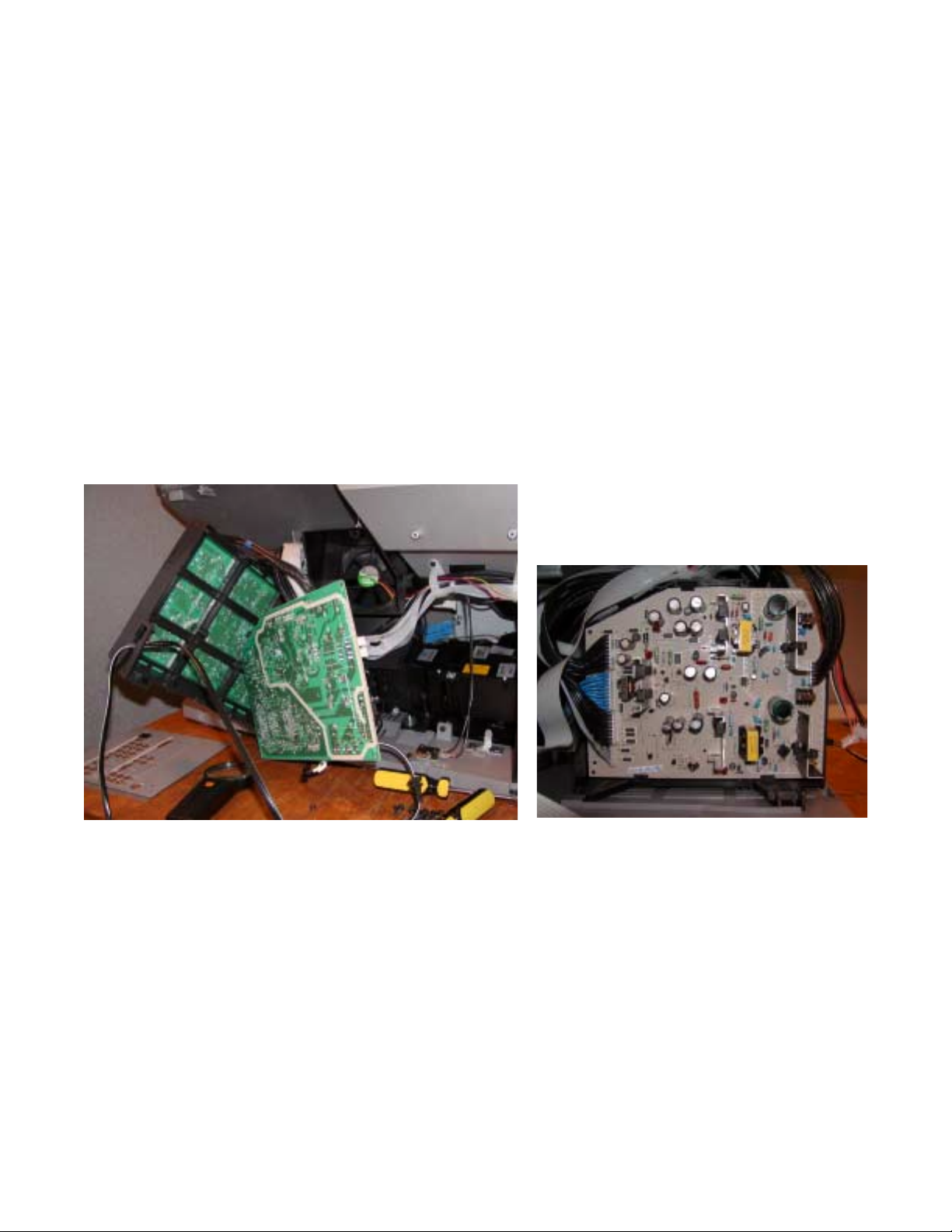
POWER BOARD SERVICE
POSITION
Page 13
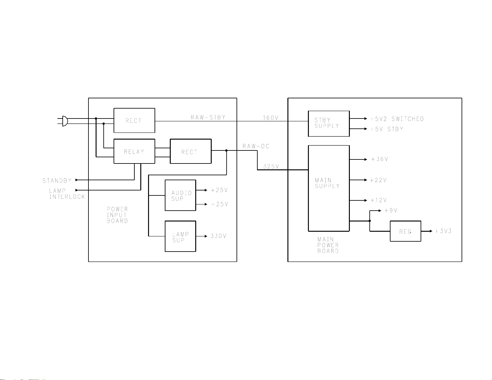
FIGURE 21 - POWER SUPPLY BLOCK
Page 10
Page 14
Page 11
FIGURE 22 - AC INPUT CIRCUIT
Page 15

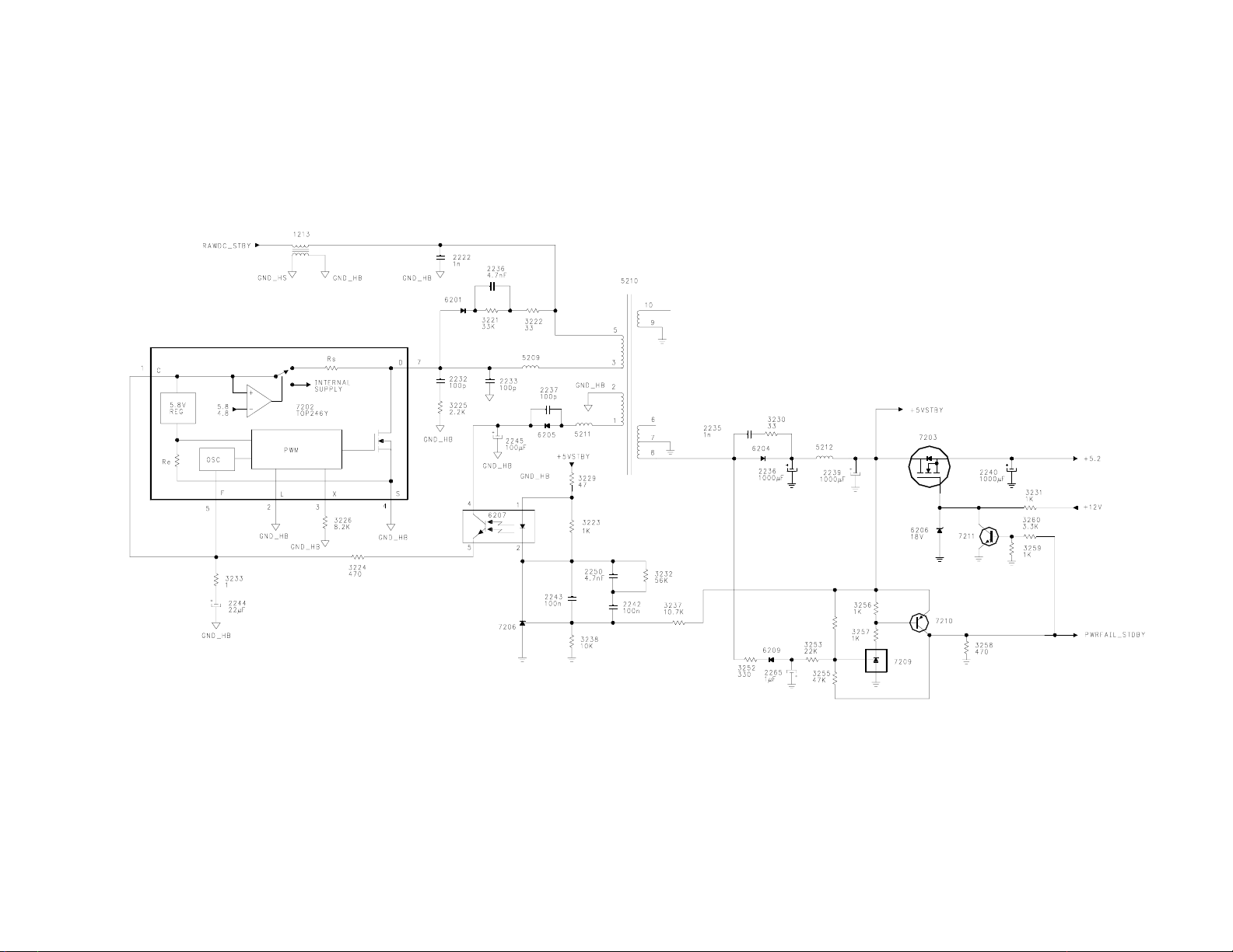
STANDBY SUPPLY (Figure 23)
The Standby supply is located on the Main Power board. It provides the +5VSTBY supply to
the set whenever power is applied.
When power is first applied, the RAWDC_STBY is applied to the primary winding of 5210 and
to Pin 7 of 7202. Current through resistor Rs charges Capacitor 2244 connected to Pin 1 of
7202. When the charge on 2244 reaches 5.8 volts, the Internal Supply switch is switched to
internal. The Oscillator and PWM turn On to drive the internal FET. The PWM will continue
to drive the FET until the charge on Capacitor 2244 drops below 4.8 volts. Capacitor 2244
will again charge and the process will repeat. With each startup cycle, energy is transferred
to the secondary windings of 5210. When the +5VSTBY supply reaches 5 volts, the input of
7206 will go to 2.5 volts. This will turn Shunt Regulator 7206 On, causing current to flow
through optoisolator 6207. Voltage from Pins 1 and 2 of 5210 is rectified by 6205 to produce
the operating voltage for 7202. When Optoisolator 6207 turns On, the operating voltage is
applied to Pin 1 of 7202. The supply is in a normal operating mode.
Regulation of the secondary is accomplished by monitoring the reference voltage via Shunt
Regulator 7206 and optoisolator 6207. The +5VSTBY is the reference voltage for the
Standby supply. If the 5-volt standby supply should increase, Shunt Regulator 7206 will conduct harder, causing the LED in Optoisolator 6207 to get brighter. The internal resistance of
the transistor inside 6207 will be reduced. The internal regulator inside 7202 connected to
Pin 1 works to keep Pin 1 at 5.8 volts. If the current through 6207 increases, the current flow
through the 5.8-volt regulator will increase. This increase in current will cause the voltage
across the sensing resistor Re to increase. The PWM will then reduce the On time of the
internal FET, reducing the secondary voltage. If the 5-volt standby voltage should decrease,
the current through the sensing resistor Re will decrease, reducing the voltage across the
resistor. This will cause the PWM to turn the internal FET On for a longer period of time,
increasing the secondary voltage.
The +5.2 volt supply is switched by FET 7203 when the +12 volt supply from the Main Power
supply is switched On. If the Standby Supply should fail or Power is removed from the set,
the Standby Power Fail circuit will signal the Microprocessor in time to allow it to shut down.
Voltage from Pin 8 of 5210 is rectified by 6209 to produce a negative voltage. This voltage
and the +5 volt standby voltage is applied to the input of Shut Regulator 7209. The combined
voltage keeps the input to 7209 below the turn On voltage of 2.5 volts. A small Capacitor,
2265, filters the negative voltage that is rectified by 6209. If power is removed from the set,
2265 will discharge quickly because of its small value. The input to 7209 will then go above
2.5 volts, turning it On. This will turn transistor 7210 On, switching the Standby Power Fail
line High. Transistor 7210 will also turn On, turning the +5.2 volt supply Off.
Page 12
Page 16
Page 13
FIGURE 23 - STANDBY SUPPLY
Page 17

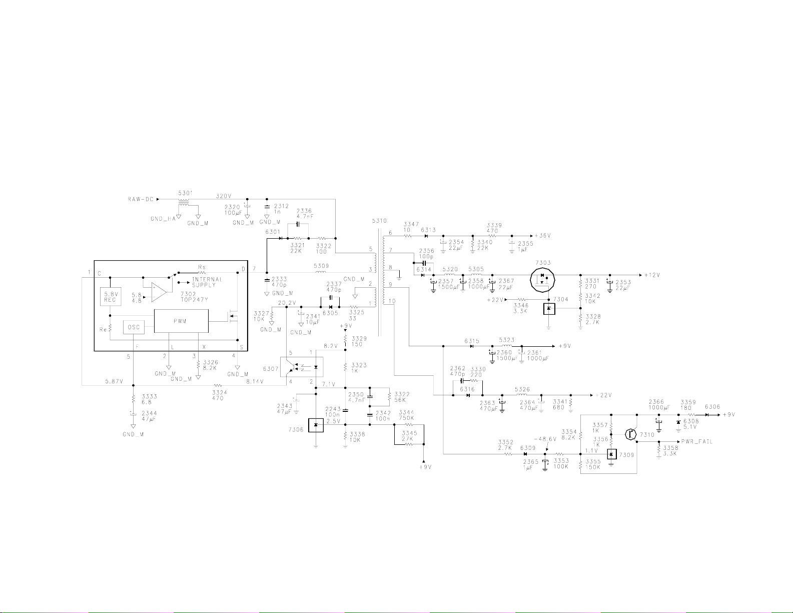
MAIN POWER SUPPLY (Figure 24)
Power is applied to the Main Power supply when the set is turned On. The RAW-DC is
switched to the Main Power supply located on the Main Power supply board. Voltage is
applied to the Primary winding of 5310 via Pins 5 and 3. Voltage is then applied to Pin 7 of
7302. In the Startup mode, voltage from the internal current limiting resistor Rs is routed to
Pin 1 where it charges Capacitor 2344. When the charge on Capacitor 2344 reaches 5.8
volts, Pin 1 is switched to the Internal Supply connection. The Oscillator and PWM drive are
switched On to drive 5310. IC 7302 will continue to drive the Transformer, 5310, until the
charge on 2344 drops below 4.8 volts. The Startup cycles will continue until the secondary
reference voltage, the 9 volts supply, reaches the correct level. When the 9-volt supply
reaches the correct level, 2.5 volts will be applied to the input of Shunt Regulator 7306.
Shunt Regulator 7306 will then turn On causing current to flow through the LED in
Optoisolator 6307. This will turn the transistor inside 6307 to turn On. Voltage from Pins 1
and 2 of the Hot secondary is rectified by 6305 and filtered by 2341. Optoisolator 6307
switches this voltage to Pin 1 of 7302 to provide the operating voltage for the IC.
The secondary produces +36, +12, +9, and +22 volt supplies. Shunt Regulator 7304 and
FET 7303 regulate the +12 volt supply.
The PWR_FAIL Main Power Fail detection circuit signals the Microprocessor when power is
about to be lost to the set while it is On. Voltage from Pin 9 of 5310 is rectified by 6309 to
produce a negative voltage, which is filtered by Capacitor 2365. This voltage along with the
+9 volt supply is applied to the input of Shunt regulator 7309 via resistor network of 3354,
3355, and 3353. As long as the negative voltage is present on 2365, the voltage on the input
of 7309 will be less than the 2.5 volts necessary to turn it On. Transistor 7310 will be turned
Off, keeping the PWR_FAIL line Low. When the switched mode supply ceases operation,
Capacitor 2365 will discharge quickly, due to its low value, allowing the voltage on the input of
7309 to increase to 2.5 volts. Shunt Regulator 7309 will turn On, turning transistor 7310 On,
causing the PWR_FAIL line to go High. This will signal the Microprocessor to shut everything
down before the main supply voltage drops.
Regulation of the secondary is accomplished by monitoring the reference voltage, the +9 volt
supply, to control the On time of the internal FET of 7302. If the +9 volt supply increases,
Shunt Regulator 7306 will conduct harder increasing the amount of current through 6307.
This will cause the LED to increase in brightness, reducing the internal resistance of the transistor inside the IC. The increase in current will cause the voltage across the internal sensing
resistor Re inside 7302 to increase. The PWM will then reduce the On time of the internal
FET, decreasing the secondary voltage. If the +9 volt supply should decrease, 7306 will conduct less, the transistor inside 6307 will conduct less, causing less current to flow through the
sensing resistor Re. The PWM will sense the lower voltage across Re, increasing the On
time of the internal FET to increase the secondary voltage.
Page 14
Page 18
Page 15
FIGURE 24 - MAIN POWER SUPPLY
Page 19
3.3 VOLT REGULATOR (Figure 25)
IC 7307 and transistor 7308 make up the 3.3-volt regulator located on the Main Power Supply
board. When the Oscillator in 7307 goes Low, the flip-flop is reset causing Q to go Low and
the output to go High. When the Feedback voltage on Pin 5 is below 1.25 volts, the
comparator outputs a High. When the Oscillator goes High, the flip-flop is Set, causing Q to
go High. This causes Pin 1 to go Low, turning Transistor 7308 On. 7308 will stay on until the
Oscillator goes Low, resetting the flip-flop. If the output voltage monitored on Pin 5 goes
below 3.3 volts, the voltage on Pin 5 will drop below the 1.25 volt reference. The flip-flop will
then Set when the Oscillator goes High. If the output voltage goes above 3.3 volts, the
reference voltage on Pin 5 will be above the 1.25 volt internal reference. The flip-flop will not
Set when the Oscillator goes High until the feedback reference voltage on Pin 5 drops below
the 1.25 volt internal reference. This method controls the On time of 7308 to regulate the
3.3-volt supply. Pin 7 monitors the current by reading the voltage drop across resistors 3349
and 3351. If the output current is excessive, the Oscillator will go Low to shorten the On time
of 7308.
POWER INPUT BOARD IN SERVICE POSITION
MAIN POWER BOARD
Page 16
Page 20
Page 17
FIGURE 25 - 3.3-VOLT REGULATOR
Page 21

AUDIO POWER SUPPLY (Figure 26)
The Audio supply produces a plus and minus 23 volts. This supply is located on the Power
Input board. The Audio supply also produces the CONTROL-VOLTAGE or operating voltage
for the Lamp supply.
RAW-DC voltage is applied to the Audio Power supply circuit when the set is turned On. This
voltage is applied to primary windings, Pins 5 and 3, of Transformer 5410. It is also applied to
Pin 7 of the Switching Regulator, IC 7402. Startup occurs when the voltage applied to Pin 7
is fed to the current limiting resistor Rs and to Pin 1 of the IC. This voltage charges Capacitor
2444. When the voltage on this Capacitor reaches 5.8 volts, Pin 1 is switched to the Internal
Supply. The Oscillator and PWM drive turns On to drive the internal FET. This drives 5410 to
produce the secondary voltages. The IC will continue to operate until the charge on 2444
drops below 4.8 volts. The Startup cycle will then repeat. When the secondary voltages
have reached the correct level, the input to Shunt Regulator 6404 will increase to 2.5 volts.
Shut Regulator 7406 will then turn On, switching Optoisolator 6404 On. The voltage on Pin 1
and 2 of 5410 is rectified by 6405 and filtered by Capacitor 2441. This voltage is then
switched by Optoisolator 6404 to Pin 1 of 7402 to provide the operating voltage. The supply
is then operating in a normal mode. The operating voltage from 6405 is also used to supply
the CONTROL-VOLTAGE supply to the Lamp supply.
Regulation is accomplished by monitoring the Positive Audio supply. This voltage is fed to
resistor network, 3444, 3445, and 3438. It is then fed to the input of Shunt Regulator 7406.
If the secondary voltage should increase, Shut Regulator 7406 will conduct harder, increasing
the current through the LED in Optoisolator 6404. This will decrease the internal resistance
of the Transistor inside 6404. The 5.8-volt regulator inside 7402 keeps Pin 1 at 5.8 volts. To
maintain this Pin at the correct voltage, the Regulator will increase the current through the
sensing resistor Re. The voltage across Re is fed to the PWM which reduces the On time of
the Internal FET, which reduces the output voltage. If the secondary voltage should
decrease, the voltage across Re would decrease via the same path. The PWM would then
increase the On time of the internal FET to increase the secondary voltage. In some cases,
the secondary load could become excessive on the positive supply causing the voltage on
the other windings of 5410 to increase. If the voltage from Pin 1 of 5410 should exceed 23.8
volts, Zener diode 6404 will conduct, increasing the current through the sensing resistor Re to
reduce the On time of the internal FET to prevent damage to the supply.
The Audio supply can also be shut down if a DC-FAULT is detected in the Audio Output circuit or if the positive and negative supplies become unbalanced. In normal operation, the DCFAULT line is Low, turning Transistor 7412 On. This turns Transistor 7411 On, which turns on
Optoisolator 6410. This connects resistor 3403 and Pin 3 of 7402 to ground. This enables
the Switching Regulator IC 7402. If Pin 3 is open, 7402 will shut down. If the DC_FAULT line
should go High, 7412 will turn Off, turning 7411 and the Optoisolator 6410 Off. This will shut
the supply down. The positive supply is connected to diodes 6407 and 6409 via resistor 3460.
The negative supply is also connected to the same point. When the supplies are equal, the
voltage at this point is zero. If the voltage becomes unbalanced in the negative direction by -
2.5 volts, Transistor 7410 will turn On, turning Transistor 7409 On. This will turn Transistor
7411 Off, shutting the supply Off. If the voltage becomes unbalanced in the positive direction
by 1.2 volts, Diode 6409 will conduct, turning Transistor 7409 On, turning 7411 Off, shutting
the supply down.
Page 18
Page 22
Page 19 FIGURE 26 - AUDIO POWER SUPPLY
OPERATING VOLTAGE FOR
THE LAMP SUPPLY
REGULATOR
Page 23

LAMP SUPPLY (Figure 27)
The Projection requires a minimum of 330 volts to operate. To ensure that sufficient voltage
is present, a Boost Regulator is used. A Boost Regulator has a higher output voltage than
the input voltage. The Lamp supply is located on the Power Input board.
RAW-DC-LAMP is applied to the Boost circuit via Fuse 1511. Voltage is applied to Pin 1 and
Capacitor 2544 via the current limiting resistor Rs in 7502. When the charge on 2544
reaches 5.8 volts, the PWM circuit drives the internal FET. When the FET is On, a field
builds up in Coil 5510. 5509 is a Ferrite bead to reduce RFI. When the FET turns Off, the
field in 5510 reverses. This voltage is rectified by Diode 6501, which charges Capacitor
2534. This will continue until the charge on 2544 drops below 4.8 volts. The Startup cycle
will then repeat. When the voltage across 2534 reaches 330 volts, Shunt Regulator 7506
turns On, turning Transistor 7500 On. The Control Voltage from the Audio Power supply now
becomes the operating voltage for Pin 1 of 7502.
Regulation is accomplished by the monitoring of the 330 Lamp voltage by Shunt Regulator
7506. If the 330-volt supply increases, 7506 will turn On harder, turning Transistor 7500 On
harder. The increase in current will increase the voltage across the sensing resistor Re inside
7502. The Regulator connected to Pin 1 will keep Pin 1 at a constant 5.8 volts. The voltage
across Re will be fed to the PWM, reducing the On time of the internal FET to reduce the
output voltage.
If the Switch mode circuit for the Lamp supply failed to operate, the voltage to the Lamp
would be equal to the RAW-DC-LAMP voltage. The symptom is this case would be that the
lamp would not ignite. Another possibility would be that 7502 might short. There would not
be Lamp voltage in this case. A Low output voltage might be caused by the feedback circuit,
7506 and 7500, failing to operate. A Scope reading on Pin 1 of 7502 would indicate that the
voltage would be changing between 4.8 and 5.8 volts. Pin 7 of 7502 would be pulsing On
and Off.
Page 20
Page 24
Page 21
FIGURE 27 - LAMP SUPPLY
Page 25
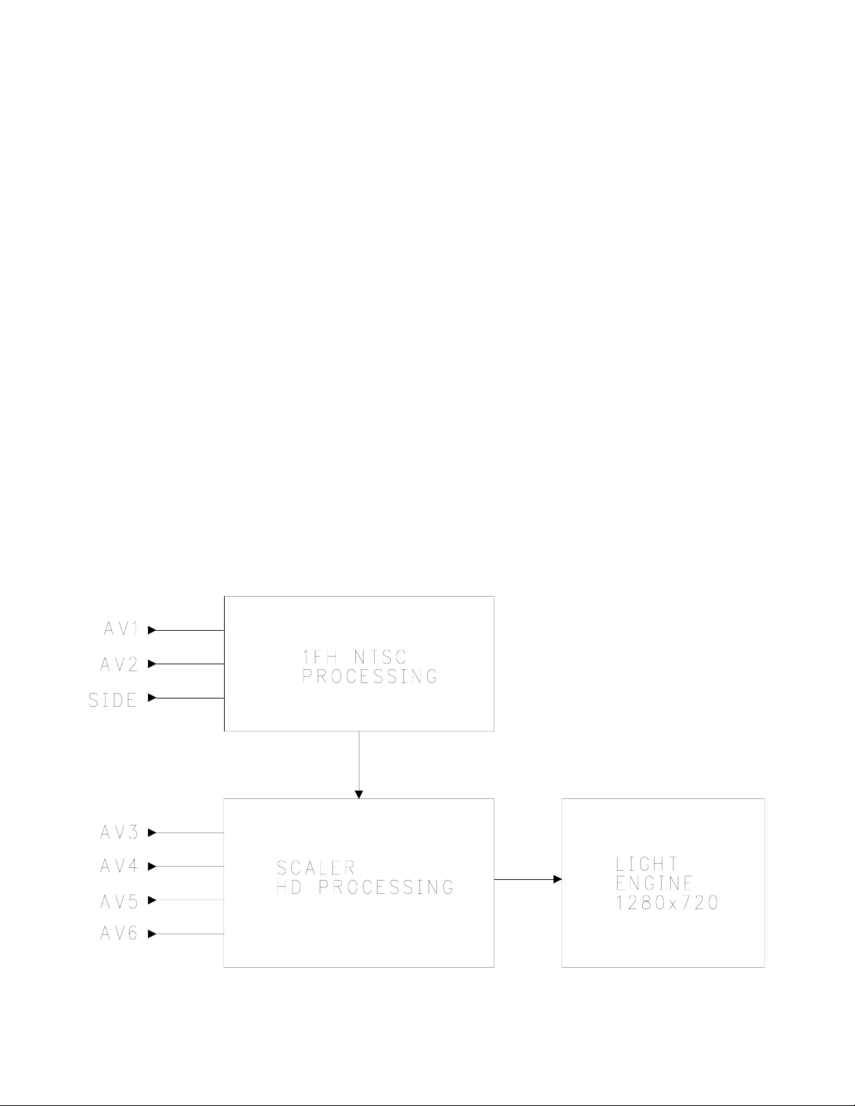
VIDEO SIGNAL FLOW BLOCK (Figure 28)
The LCOS projector has three sections:the 1FH NTSC processing, Scaler HD Processing,
and the Light Engine.
The 1FH NTSC section has three video inputs, AV1, AV2, and Side, which are for NTSC
composite video only. This section has Line Doubling, Pixel Plus, and Picture in Picture functions. The 2FH signal from this section is fed to the Scaler HD Processing section.
The Scaler HD Processing section has two Y Pb Pr inputs, AV3 and AV4. AV5 is a RGB
input while AV6 is a DVI input. AV3 and AV4 can accept either a 1H NTSC signal, a 480P
signal, or a 1080I HD signal. For best results, the 1FH signals should be connected to AV1,
AV2, or the Side input. It also processes the 2FH signal from the 1FH NTSC section. The
Signal is processed to output a 1280x720 pixel to the Light Engine. The Light Engine contains all of the display circuits used to project the picture to the screen.
1FH PROCESSING IS FOR NTSC ONLY
PIXEL PLUS PROCESSING IN THE 1FH SECTION
EITHER 1FH OR 2FH SIGNAL CAN BE APPLIED TO THE SCALER
REGARDLESS OF THE SOURCE ALL SIGNALS ARE
DISPLAYED IN A 1280x720 FORMAT
FIGURE 28 - VIDEO SIGNAL FLOW BLOCK
Page 22
Page 26
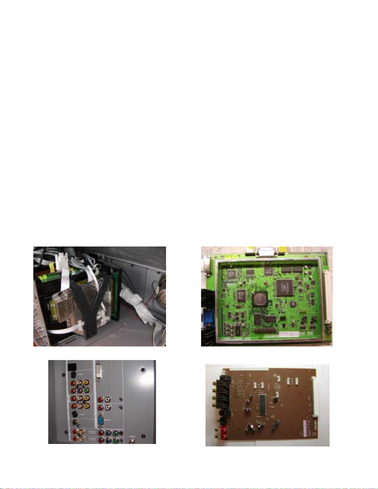
FIGURE 29 - OVERALL BLOCK 1FH SECTION (Figure 29)
The inputs for the 1FH section are for NTSC signals only. The Side Jack panel can accept
either composite video or SVHS video. The Composite video or YC from the Side Jack Panel
is fed to the Jack Panel. Two Composite or SVHS inputs, AV1 and AV2 are located on the
Jack Panel. These inputs, along with the input from the Side Jack panel, are fed to the 7100
switch. IC 7100 selects between the three composite or SVHS inputs for output to the SSB
and PIP/DW boards via the System board. A Y Pb Pr 1FH input is also located on the Jack
Panel. This signal is converted from Y Pb Pr to YUV on the System board before being fed
to the SSB. This YUV signal is also fed to the PIP/DW panel. IF from the main Tuner, located on the System board, is also fed to the SSB.
The HIP IC on the SSB selects between the internal Tuner video or selected video from the
Jack panel. If the signal is Composite video, it is fed to a 3D Comb filter panel for processing. YC from the 3D Comb filter is fed back to the HIP. The HIP then outputs YUV to the
PIP/DW panel, which inserts the Picture in Picture or Split Screen when selected by the customer. The Picture in Picture or Split Screen video is selected from the YUV signal, the
selected video from the Jack Panel switch, or the Tuner located on the PIP/DW panel. YUV
from the PIP/DW is then fed to the Feature Box, which performs the line doubling and zooming features. YUV from the Feature Box is then fed to the Eagle circuit, which enhances the
picture. The Pixel Plus feature is performed in the Eagle if the set is programmed for the
Pixel Plus feature. The YUV output from the Eagle is then fed to the LVDS transmitter before
being sent to the Scaler board. The video signal is digitized in the Feature Box and remains
digitized from that point on.
SSB SMALL SIGNAL BOARD
JACK PANEL
Page 23
MSB MAIN SCALER BOARD
JACK PANEL BOARD
Page 27
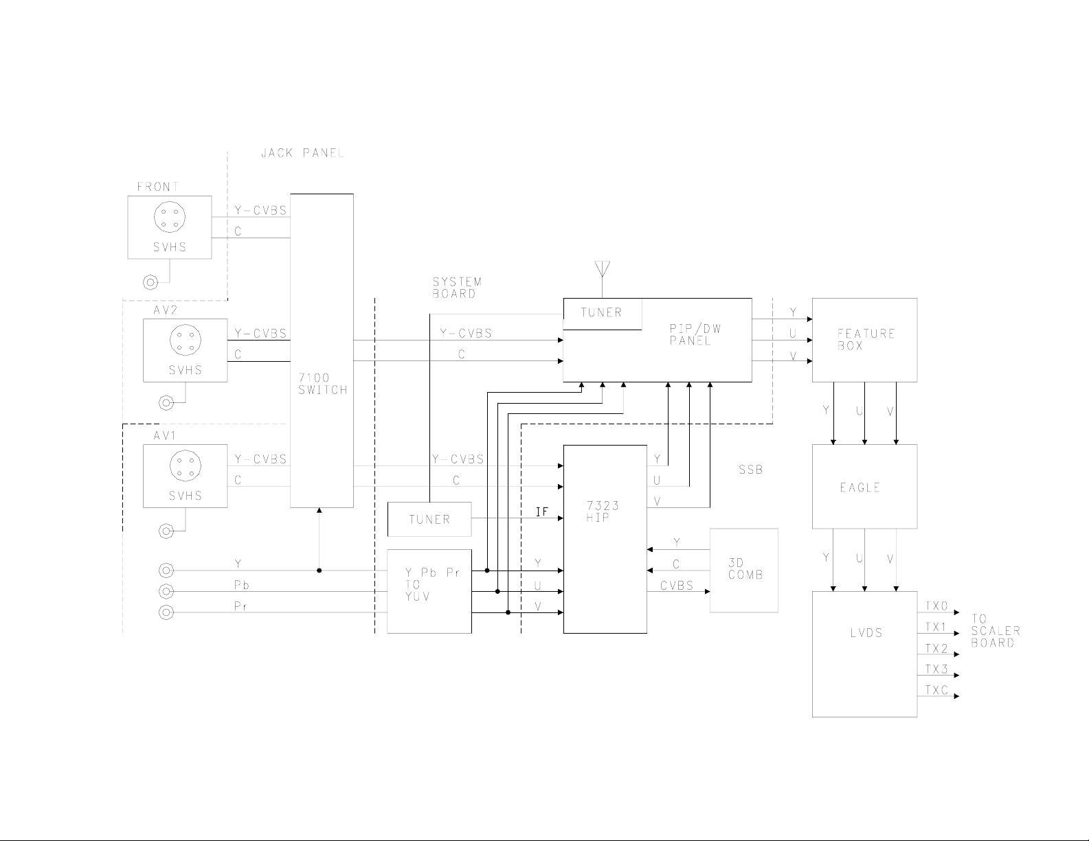
FIGURE 29 - OVER BLOCK - 1FH SECTION
Page 24
Page 28
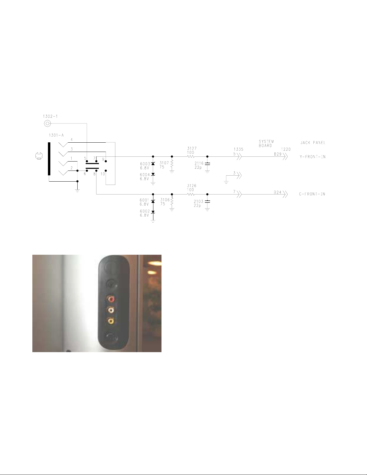
SIDE JACK PANEL (Figure 30)
The Side Jack panel can have either a composite or SVHS input. When a connector is
inserted into the SVHS input, the composite input is disconnected. Zener diodes are connected to both the Y/composite and the C lines to limit the applied voltage to 7.4 volts. A 75ohm resistor on both lines provides the correct impedance matching. The Y/composite and C
signals are output to the Jack panel via the System board.
SIDE JACK PANEL
FIGURE 30 - SIDE JACK PANEL VIDEO
Page 25
Page 29
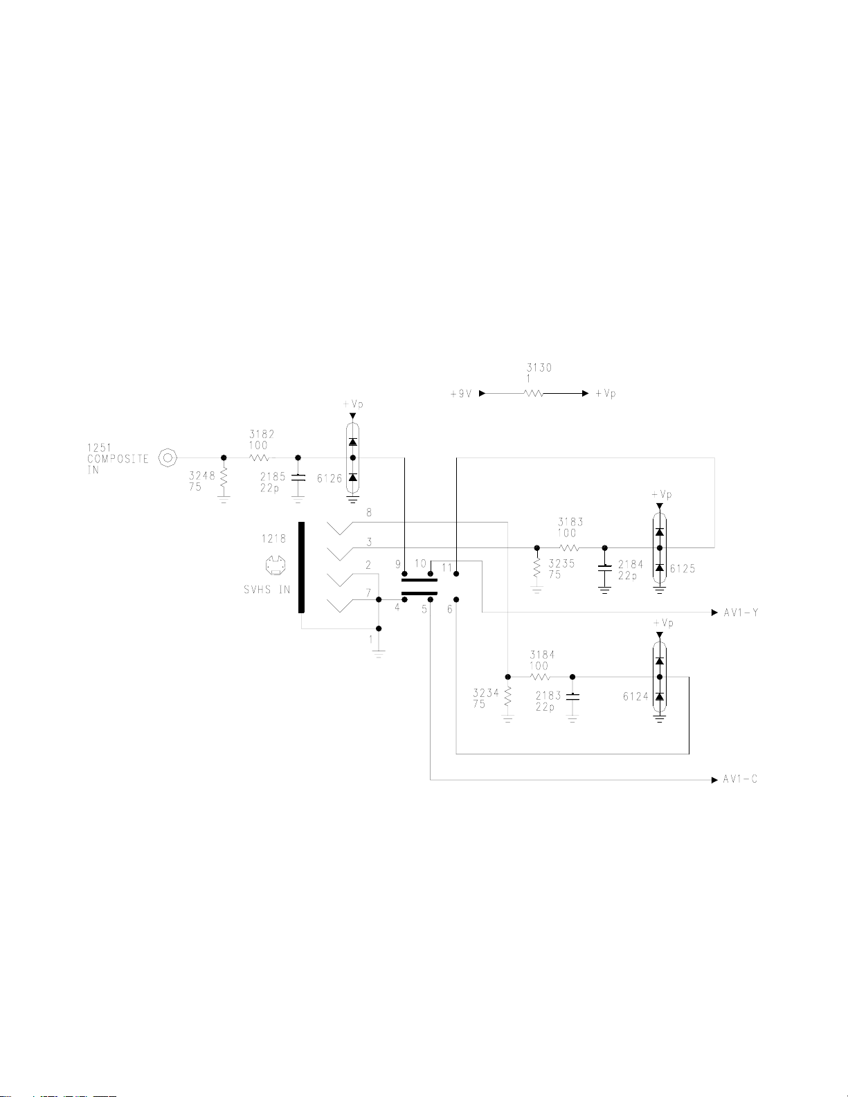
AV1 INPUT (Figure 31)
The AV1 and AV2 inputs are located on the Jack panel. Composite video for AV1 is input to
connector 1251 and then to an impedance matching network consisting of resistors 3248 and
3182. Diode array 6126 prevents the incoming signal from exceeding 9.6 volts in the positive
direction and 0.6 volts in the negative direction. When a connector is placed in the SVHS
jack, the Composite video input is disconnected. The Y signal is routed through an impedance matching network and clamp and back to Pin 11 of 1218. The C signal is also routed
through an impedance matching network, clamped to Pin 6, and output on Pin 5. The clamping voltage +Vp is supplied by the +9 volt source. The AV2 input is identical except for the
component input.
FIGURE 31 - AV1 INPUT CIRCUIT
Page 26
Page 30
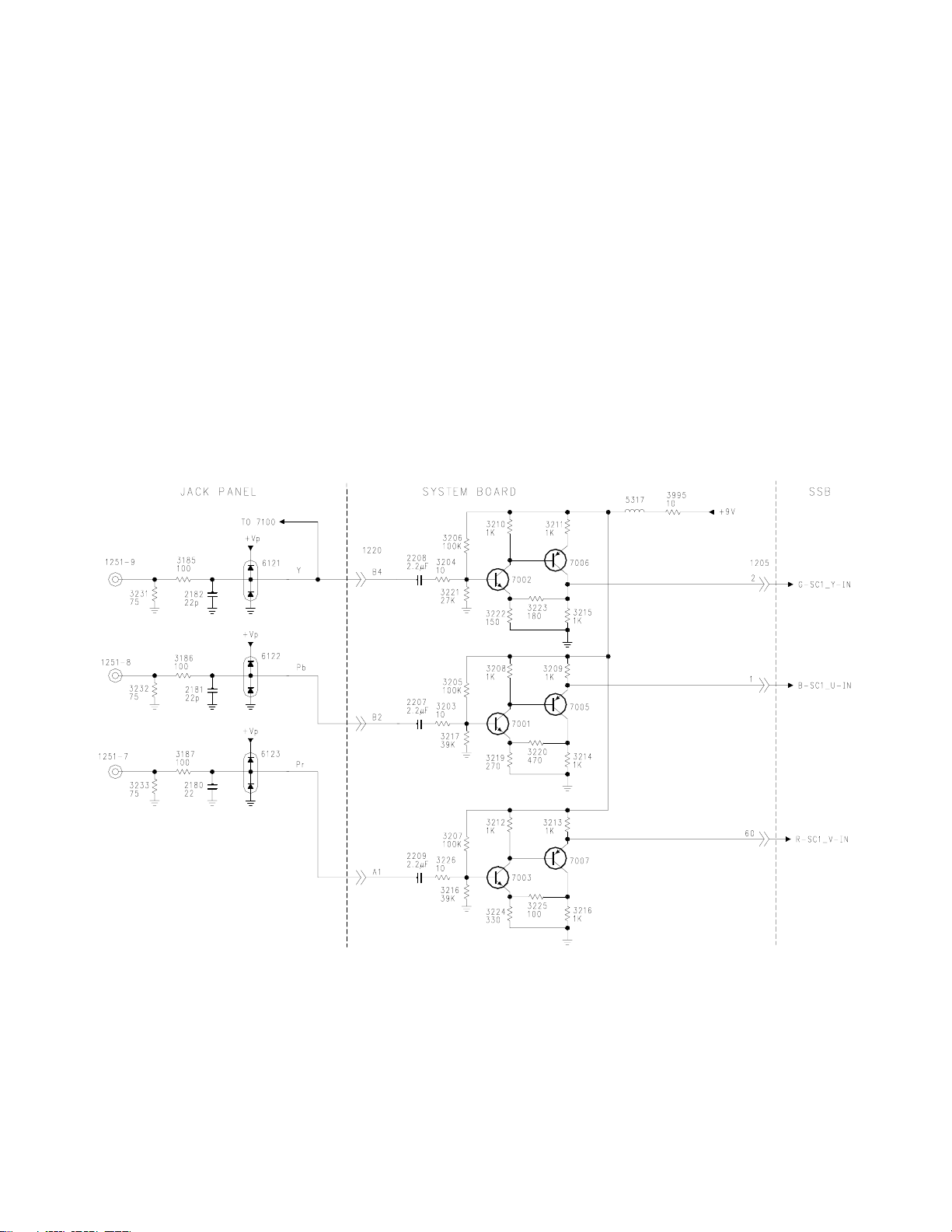
1H COMPONENT INPUT (Figure 32)
The 1FH Y Pb Pr inputs are located on the Jack panel. The 1H Y Pb Pr inputs all have an
impedance matching resistor and clamping circuit. As with the composite and SVHS inputs,
the input signal is clamped to be no more that 0.6 volts above the +Vp supply in the positive
direction and no more than 0.6 volts in the negative direction. The clamping voltage +Vp is
supplied by the +9 volt source. The Y signal is also fed to IC 7100 for Sync separation.
The Y Pb Pr signals are fed to the System board via connector 1220. The circuit on the
System Board converts the signals from a Y Pb Pr format to a YUV format. To provide proper impedance matching, Transistors 7002 and 7006 buffer the Y signal. Transistors 7001 and
7005 phase invert the Pb signal to convert it to a U signal. Transistors 7003 and 7007 phase
invert the Pr signal to convert it to a V signal. The converted YUV signals are fed to the SSB.
Page 27
FIGURE 32 - 1FH COMPONENT INPUT CIRCUIT
Page 31

1FH JACK PANEL SWITCHING (Figure 33)
The switching for the composite and SVHS signals is performed by IC 7100, located on the
Jack panel. IC 7100 is controlled by the SDA_EMG and SCL_EMG bus that comes from the
OTC (main Microprocessor) located on the SSB. The Y signal from the Y Pb Pr input is fed
to Pin 5, where it is switched to the System board and the SSB. This signal is used to provide Sync separation when the Y Pb Pr input is used. There are two sets of switches used
for the composite input. The output on Pin 39 switches selected video to the PIP/DW panel
for display in the Picture in Picture or Split Screen window. Pin 35 outputs the C signal for
the PIP/DW circuit. The selected composite video for the main picture is output on Pin 1
while the selected C signal is output on Pin 3.
FIGURE 33 - 1FH JACK PANEL SWITCHING
Page 28
Page 32

MAIN TUNER (Figure 34)
The Main tuner is located on the System board. The IF output from this Tuner is fed to the
SSB for processing. The 36-volt supply from the Main Power supply board supplies the tuning voltage. This voltage is regulated by Zener diode 6112 and Shunt Regulator 7115 to produce 33 volts. The 33-volt supply is also fed to the PIP/DW panel to supply the tuning voltage for that Tuner. The +5 volt supply is also fed to Pin 6 and 7 of the Tuner.
Page 29
FIGURE 34 - MAIN TUNER
SYSTEM BOARD
Page 33

HIP (High end Input Processor) CIRCUIT (Figure 35)
The IF from the Main Tuner and selected composite or SVHS signals is fed to the HIP IC
7323 located on the SSB. This IC is controlled by the SDA-F and SCL-F, fast bus, from the
OTC (Microprocessor) located on the SSB. The IF signal is fed to 1408, SAW Filter, and then
to Pins 2 and 3 of 7323. The detected video is output on Pin 10 of 7323 and buffered by
Transistor 7411. The video signal is fed to 1411, separating the 4.5MHz Audio signal. This
signal is buffered by 7410 before being fed to the Audio processor. The video is also fed to
1407, a 4.5MHz Sound Trap, buffered by Transistor 7322, and fed to Pin 14 of 7323. If the
user has selected the Tuner as the main picture, 7323 will switch the composite video to Pin
26. The video is then buffered by Transistor 7320 before being output to the 3D Comb Filter
board. YC from the Comb Filter board is then fed back to 7323 via Pins 28 and 29. If the
user has selected external composite video, this signal is fed into 7323 on Pin 20. If the user
has selected an external SVHS signal, the YC signal is fed to 7323 via Pins 20 and 21. The
selected Y signal is fed to a delay and the selected C signal is fed to a demodulator that converts the signal to a UV signal. The YUV switch selects from the internally decoded video or
the external YUV from the Y Pb Pr inputs. The YUV signal is then fed to the PIP/DW circuit
for insertion of the Picture in Picture or Split screen. Horizontal Sync is output on Pin 60
while Vertical Sync is output on Pin 61.
Page 30
Page 34

Page 31
FIGURE 35 - HIP CIRCUIT
Page 35

NTSC COMB FILTER CIRCUIT (Figure 36)
The Comb Filter circuit separates the Chrominance and Luminance, YC, from the composite
video. This is a separate PC board that plugs into the System board. The video signal is
amplified by Transistors 7008 and 7009. Transistors 7010, 7015, 7016, and 7017 separate
the Sync from the composite video. The Sync is fed to Pin 76 of 7023. If non-standard Sync
is detected, as with a video game, 7023 performs a 3-line sync separation. The composite
video is buffered by 7011 and fed to a 6MHz filter, 5006. This prevents any high frequency
signals from causing problems with the A/D conversion. The signal from 5006 is buffered by
Transistor 7012 and fed to Pin 88 of 7023. A Clamp circuit sets the sampling range of the
A/D converter. A full frame 3D YC separation is performed by the YCS circuit. The YC signal
is then output to two D/A converters that output C on Pin 83 and Y on Pin 84. The Y signal is
buffered by 7003 before being fed to a 6MHz filter to remove any high frequency components
generated by the D/A conversion. The signal is then buffered by Transistors 7002, 7001, and
7000 before being fed back to the SSB via the System board. A similar circuit also filters the
C signal.
COMB FILTER INSERTED INTO SYSTEM BOARD
Page 32
Page 36

Page 33 FIGURE 36 - NTSC COMB FILTER CIRCUIT
Page 37

PIP/DOUBLE WINDOW INPUT (Figure 37)
The PIP/Double Window panel allows for both a standard PIP window and a split screen.
The PIP/Double Window module has a separate Tuner, SAW filter, and Signal Processor.
The output of the Signal Processor, 7301, on Pin 16 is fed to switching IC 7402 that selects
between the PIP Tuner and Composite Video from the SSB. Selected Composite Video for
the main picture is output on Pin 15 of 7402 and is fed to the SSB. Selected Composite
Video for the PIP window is output on Pin 14 and is buffered by 7421. It is fed to 1333, a
4.5MHz Trap. It is then buffered by transistor 7331 before being fed to Pin 24, which selects
between the selected Tuner Video or selected Composite Video from the SSM. Composite
Video is fed to a YC separator, then to a Delay Line and Demodulator. If it is a YC signal, it
bypasses the YC separator. The YUV signal is then fed to the YUV switch, which selects
between the output of the Delay Line and Demodulator, and external YUV from the Large
Signal Board. The YUV (SY, SU, and SV) is output to the PIP processor IC. Selected
Composite Video is fed to the V-Chip processor. V-Chip processing for the main picture is
done by the Microprocessor on the SSB.
DOUBLE WINDOW PIP OUTPUT (Figure 38)
The PIP or Double Window YUV signal is fed to the PIP/DW processor, 7801. The I2C buss
controls the IC from the Microprocessor on the SSB. The PIP/DW processor outputs YUV for
the PIP window or Split Screen to the YUV switch, 7803, where it is mixed with the YUV signal from the SSB for the main picture. The Fast Blanking line from 7801 on Pin 68 controls
the switch point in which the PIP window or Split Screen is inserted. The +3VD line switches
the SDA and SCL lines. The PIP processor is powered by the +3 volt supply. The +3.3 volt,
+3 volt, and +3VD volt supplies are produced by regulator 7802 which is driven by the +5VS
supply. This supply is switched On when the PIP window is selected.
DOUBLE WINDOW CONTROL AND POWER SUPPLY (Figure 39)
The PIP/Double Window module is controlled by the I2C buss through 7403 on the PIP module. Pins 4, 5, 6, and 7 perform Video selection functions. Pin 10 produces a reset signal for
the Guide Plus module. Pin 12 controls the +5VS and +8VS supplies.
PIP/DW PANEL
Page 34
Page 38

Page 35
FIGURE 37 - PIP/DOUBLE WINDOW INPUT
Page 39

FIGURE 38 - PIP/DOUBLE WINDOW OUTPUT
Page 36
Page 40

Page 37
FIGURE 39 - DOUBLE WINDOW CONTROL AND POWER SUPPLY
Page 41

FEATURE BOX (Figure 40)
The circuit located on the SSB, labeled the Feature Box, performs the digitizing, line doubling,
and picture resizing. The main functions are performed by 7611, PICNIC (PICture improvement Network IC), and 7718, FALCONIC (Field And Line COnverter and Noise reduction IC).
The PICNIC IC performs the A/D Analog-to-Digital, conversion while the FALCONIC performs
the Line Doubling. The FALCONIC also performs the Super Zoom, Panoramic, 4:3, Movie
Expand 14:9, Movie Expand 16:9, 16:9 Subtitle, and Widescreen picture format conversions.
The YUV signal is fed to the PICNIC on Pins 23, 25, and 26. Horizontal and Vertical Sync is
fed to the IC on Pins 28 and 29. The signals are fed to a Clamping circuit to limit the sampling range, an AGC, and a Prefilter circuit. It is then fed to a triple A/D converter, Time Base
Corrector, Noise Reduction and Histogram circuit, and a Multiplexer. The Prefilter circuit limits the bandwidth of the signals to prevent aliasing. Aliasing shows up as artifacts in the picture, which is caused by under sampling. The Multiplexer combines the three data streams
into one.
Data is output from the PICNIC to FM1 (Field Memory), IC 7714. The Fields are read by
7718 to the Dynamic Noise Reduction circuit and to the processor. The De-Interlace writes
the Field data to Field Memory 2, 7717 and Field Memory 2, 7719. The Processor then reads
the Field memories to convert the signal to a progressive scan signal. A Motion Estimator
processes moving blocks in the picture to produce a natural motion. The processors resize
the picture to fit the format selected by the user. However the picture appears to be formatted, the output is always a 480P format. The Signal is output on two 16-bit busses, F and G,
to the Eagle processor.
The FALCONIC is controlled by the Microprocessor in the PICNIC. The PICNIC is controlled
by the Fast clock and data line from the OTC. The PICNIC communicates with the FALCONIC and the Eagle via the SN clock and data line. This is called a SNERT interface. SNERT
is a Synchronous No parity Eight-bit Reception and Transmission interface.
PICNIC IC
FALCONIC IC
Page 38
Page 42

Page 39
FIGURE 40 - FEATURE BOX
NOT
USED
Page 43

EAGLE (Figure 41)
The Eagle circuit provides Skin tone correction, Blue stretch, and Green Enhancement. In
versions equipped with the Pixel Plus feature, the Eagle IC performs the corrections for this
mode.
The video frames are sent to FM4 and FM5, 7722, and 7723 memories from the FALCONIC
IC. These memory ICs hold the frame data until they are required for processing by the
Eagle. The Input Multiplexer selects which frame is to be read. The Vertical and Horizontal
Peaking circuit sharpens the edges and adds blue pixels to enhance the picture. This circuit
is part of the Pixel Plus processing.
The Scaling circuit scales the picture to 1280x720 pixels to conform to the Light Engine display. The YUV format circuit converts the picture to conform to the MSB (Main Scaler Board)
input. The Eagle is controlled by the Microprocessor in the PICNIC IC via the SNERT interface. The Eagle outputs a 8-bit digital Y and UV signal to the LVDS transmitter.
Page 40
Page 44

Page 41
FIGURE 41 - EAGLE
Page 45

LVDS TRANSMITTER (Figure 42)
The 8-bit digital Y and UV signal is fed to the LVDS (Low Voltage Differential Signaling)
Transmitter, 7100. IC 7100 converts the parallel 16-bit signal to a serial data output. The
output of the LVDS is held at 345mV to prevent RFI (Radio Frequency Interference). There
are four data pairs and one clock pair. This circuit uses an 85MHz clock and is able to transfer data up to 300 Mbytes per second. The LVDS data is then sent to the MSB (Main Scaler
Board) for further processing.
FIGURE 42 - LVDS TRANSMITTER
Page 42
Page 46

2H SECTION BLOCK (Figure 43)
The 2FH processing section is located on the MSB (Main Scaler Board). Signal is fed to this
board via the SSB via the LVDS line, VGA connector, DVI connector, or the 2H Component
inputs.
The serial LVDS data is decoded back into Y 8-bit and UV 8-bit parallel data. This data is fed
to the Scaler IC. The two 2H Y Pb Pr analog inputs, AV3 and AV4 are fed to a selection
switch, 7710. The selected Y Pb Pr is fed to 7345 that selects between the selected Y Pb Pr
and the AV5 RGB input. IC 7345 selects the desired input and performs an Analog to Digital
conversion. The three 8-bit parallel data lines are fed to the Scaler IC along with the three 8bit lines from the DVI (Digital Video Interface) connector. The Scaler can perform a 1H to 2H
conversion. It can also produce a split screen between two inputs. Therefore, it is possible
to have a split screen with the NTSC signal on one side and a HD input on the other side.
The Scaler also formats the video signal to fit the 1280x720 pixel Light Engine display. The
Scaler outputs the video data signal via three 8-bit data lines to the OSD insertion circuit.
The analog OSD (On-Screen Display) signal from the OTC is digitized and inserted into the
signal from the Scaler. The signal is then output from the OSD circuit to the TMDS where the
signal is converted from three 8-bit lines to three serial and one clock line before being fed to
the Light Engine.
Page 43
7345
SCALER BOARD
Page 47

FIGURE 43 - 2FH SECTION BLOCK
Page 44
Page 48

VGA INPUT (Figure 44)
RGB is fed to the set via AV5 using a DB15 connector. IC 7633 is loaded with the possible
settings that are read by the computer when it is connected. Some of the possible inputs to
AV5 are VGA (640x480), SVGA (800x600), XGA (1024x768), SXGA (1280x1024), HD60p
(1280x720), W-VGA (848x480), and W-XGA (1368x768). The RGB drive, Vertical, and
Horizontal Sync are all clamped to prevent excessive signal levels from being applied to the
set. The input signal is clamped to 5.6 volts in the positive direction and 0.6 volts in the negative direction.
Page 45
Page 49

FIGURE 44 - VGA INPUT
Page 46
Page 50

AV3 AND AV4 INPUTS (Figure 45)
The AV3 and AV4 inputs allow the input of Component Y Pb Pr signals from a 1080I, 480p, or
NTSC source. Better results are obtained by inserting the NTSC Component source into
AV2. Each of the AV3 and AV4 inputs are clamped to limit the level of the signals applied.
This is accomplished by using diode arrays, 6711, 6710, 6712, 6632, 6631, and 6630. The
positive portion of the signal is clamped to 5.6 volts and 0.6 volts in the negative direction.
IC 7710 selects the two AV sources. This is a High Frequency switching IC with minimal
cross talk. Pixelworks IC controls the IC via the 2FHIN1_2FH1N2 line. The Control line is
inverted by Transistor 7725, which is connected to Pin 19. When the Control line is High,
7725 turns On to pull Pin 19 Low. This selects input AV4. When the Control line goes Low,
Pin 19 goes High and AV3 is selected. To reduce interference, each section of the IC is
powered by a different 5-volt supply. The Y Pb Pr signals are output on Pins 30, 27, and 35.
The signals are then buffered by Transistors 7716, 7717, and 7715.
Page 47
AV3, AV4, AND VGA PROCESSING SECTION
Page 51

FIGURE 45 - AV3 AND AV4
Page 48
Page 52

ANALOG INPUT A/D CONVERSION (Figure 46)
The selected Y Pb Pr signal and the RGB signals from the VGA connector are fed to IC
7345. IC 7345 converts the signals from Analog to Digital. There are two triple 8-bit lines.
The GRO, GBO, and GGO lines carry the Odd field data while the GRE, GBE, and GGE lines
carry the Even field data. Sync on Y is fed to Pin 12, Sync on Green is fed to Pin 16, while
Horizontal and Vertical Sync is fed to Pins 43 and 42. The IC outputs Horizontal Sync on
Pins 125 and 126. Vertical Sync is output on Pin 127. Clock information for the data is output on Pin 123. The IC is controlled by the SDA_SCALER and SCL_SCALER lines from the
Pixelworks (Scaler) IC.
Page 49
FIGURE 46 - ANALOG INPUT AND A/D CONVERSION
Page 53

DVI INPUT (Figure 47)
AV6 is the DVI (Digital Video Interface) input. This type interface is used on some computer
video cards and Set Top boxes. This is digital transmission based on the TMDS (TransitionMinimized Differential-Signaling) format. The TMDS system provides a high-speed reduced
RFI (Radio Frequency Interference) transmission system. IC 7746 is the DVI receiver
processor.
IC 7747 stores plug and play information for the device transmitting data to the set. IC 7747
is powered by the +5VA supply when the set is operating. The connecting device can also
supply power to read the setup information from 7747. The connecting device also communicates with 7746 (DVI receiver) when the set is turned On. The connecting device provides
the format settings to 7746 via Pins 3 and 100. When the set is turned Off, Transistors 7749
and 7750 are turned Off to prevent the signal from reaching 7746. When the set is turned
On, those Transistors are turned On to connect the signal. The B+ line to 7747 and the Data
lines are clamped to 5.6 volts Positive and 0.6 volts Negative with Diode Arrays 6761, 6752,
and 6751.
There are three data pairs to 7746: RX0, RX1, and RX2. There is also a Clock line RXC connected to Pins 93 and 94. Each of these lines is clamped to prevent an excessive signal
from being applied to this circuit. The lines are clamped to 0.6 volts in the negative direction
and 3.9 volts in the positive direction. When AV6 is selected, Pins 2 and 9 are switched High
(3.3 volts). This turns 7746 On, making all of the logic circuits active. When some other
input other than AV6 is selected, all of the Outputs are put into a high impedance tri-state
mode. All of the logic circuits are powered down and the inputs are disabled in this mode.
Pin 44 transmits clock information to the Scaler IC. Pin 46 is a Data Enable line to signal the
Scaler IC that data is being output on the data lines. This line is switched High when data is
present. Pins 47 and 48 output Sync to the Scaler IC.
Page 50
Page 54

Page 51
FIGURE 47 - DVI INPUT
Page 55

LVDS RECEIVER (Figure 48)
Picture data from the SSB is transmitted to the MSB (Main Scaler Board) via the LVDS (Low
Voltage transmission system) to IC 7537. The LVDS receiver has four data lines and one
clock line.
The IC is switched On or Off by the Scaler IC via the LVDS_PWR_DOWN_n line connected
to Pin 25. When AV1, AV2, or the Front (Side) input is selected, the Scaler IC switches Pin
25 High to switch IC 7537 On. The Signal from the Eagle is output to the Scaler as digital Y
and UV. Vertical and Horizontal Sync is output on Pin 54 and 55. The Clock data signal is
output on Pin 26. The DE_EMG line goes High when the IC is switched On to signal the
Scaler IC that data is present from this IC.
FIGURE 48 - LVDS RECEIVER
Page 52
Page 56

SCALER (Figure 49)
IC 7407 is a highly integrated system on a chip that interfaces the YUV signal from the SSB,
the DVI interface, or the Analog HD inputs to the 1280x720 Light Engine. The Scaler, 7407,
is a 352 Pin Ball Grid array device.
Video Data from the Eagle for the NTSC signal is already scaled correctly in the Eagle. The
inputs from the DVI or 2H Inputs may require some Scaling. This function is performed by
the Scaler. The Scaler can also perform a 1H to 2H conversion allowing NTSC inputs into
AV3 and AV4. However, the Scaler is not as efficient as the Feature Box and Eagle on the
SSB. Therefore, 1H NTSC inputs should be applied only to AV1, AV2, or the Side input for
best results. The Scaler can also display two different inputs in a Split-Screen format. This
can be done between the NTSC inputs or one of the 2H inputs. This is not possible between
two of the 2H inputs. There are two video data inputs to 7407. The YUV input goes to the
Video Port. This is the digital video information from the SSB. AV3, AV4, AV5, and AV6 are
applied to the Graphics Port. Among the inputs that 7407 can process from the Graphics
Port are VGA, SVGA, XGA, and 1080I. The Horizontal Image Scaler, Crisp Image Scaler, and
Spatial Noise Reduction circuits perform part of the scaling functions, create the Spit Screen
if selected by the user, and make picture enhancements. The other Scaler scales the picture
to 1280x720 to meet the requirements of the Light Engine. The Scaler IC has its own internal
memory to store the frames while they are being processed.
The Microprocessor in the Scaler controls the operation of the Scaler and several external
devices. This is a slave Microprocessor of the OTC located on the SSB. The OTC communicates with the Scaler via the PLD IC. Two external memory ICs, 7406 and 7409, store the
program information for the Scaler. The NVM, 7405, stores the settings for the IC. The
Display Port outputs the processed video data on three 8-bit lines, SCR_RED, SCR_GREEN,
and SCR_BLUE.
Page 53
SCALER IC
Page 57

FIGURE 49 - SCALER
Page 54
Page 58

OSD AND OUTPUT CIRCUIT (Figure 50)
The SCR_RED, SCR_GREEN, and SCR_BLUE data is sent to the PLD (Programmed Logic
Device). The PLD inserts the digitized OSD information onto the video information. The signal from the PLD is output to the TMDS transmitter and then to the Light Engine.
The OSD information from the OTC on the SSB is in an Analog format. This information is
fed to A/D (Analog to Digital) and S/H (Sample and Hold) circuits. These circuits convert the
OSD into four 6-bit data lines before feeding the information to the PLD. As will be shown
later, the PLD is also a slave Processor that communicates with the OTC and the Scaler.
OTC OSD INPUT (Figure 51)
The OSD (On-Screen Display) signals are generated by the OTC (Microprocessor) located on
the SSB. These are Analog RGB signals with a Fast Blanking line. The OSD signals are
sent to the MSB via connector 1401. Sync for the text is generated by the PLD located on
the MSB. This Sync is fed to the OTC via the System Board.
OSD SCALER INPUT (Figure 52)
The OSD and Fast Blanking signals are converted to a digital signal and fed to the PLD
(Programmed Logic Device) to be inserted into the Picture Data. The Red, Green, and Blue
OSD is buffered and fed to two A/D (Analog to Digital) converters, 7193 and 7199. A Data
reference signal, FDB, from the PLD, along with an Upper Reference Voltage and a Lower
Reference Voltage is used to set the voltage level in which sampling will begin and end. The
ADC_CLOCK is used to clock the sampled data out of 7193 and 7199. Data is output on two
6-bit data lines to latches, 7102, 7104, and 7107 before being fed to the PLD. The CLK_RET
line clocks the data out of the Latches.
Page 55
Page 59

FIGURE 50 - OSD AND OUTPUT
Page 56
Page 60

Page 57
FIGURE 51 - OTC OSD
Page 61

FIGURE 52 - OSD SCALER INPUT
Page 58
Page 62

REFERENCE VOLTAGE AND A/D CONVERTERS (Figure 53)
The BLEND_FDB signals are fed to a resistor matrix to set the DC reference voltage for the
A/D converters. The signals are buffered by Transistors 7189 and 7188 to add bias to the
Analog FBL_OSD signal. The output of the matrix is also added to the High and Low
Reference voltages. Regulator 7185 sets the Upper Reference voltage while 7187 sets the
Lower Reference voltage. The output of the A/D converter is clocked out by the
ADC_CLOCK signal to the TTL outputs. The signal is output on a 6-bit data line. The Red,
Green, and Blue circuits work the same as this one.
INPUT LATCH AND PLD SYNC (Figure 54)
One of the three latches that are used to clock data to the PLD is shown. The OTC_BLEND
(FBLK) and two bits of the Blue are fed to Latch 7102. This data is clocked out to the PLD by
the CLK_RET line. The reference *_FDB lines are output from the PLD to set the sample reference voltage as described earlier. The DIV_ADCLK and HSYNC_PLL sync lines are used
to set the CLK_RET and ADC_CLOCK signals.
ADC CLOCK CIRCUIT (Figure 55)
The DIV_ADCLK and HSYNC_PLL signals are fed to a Phase Comparator, 7287. The Phase
Comparator drives Transistor 7282, 7280, and 7281. This circuit sets the reference voltage
for the amplifiers in 7283. IC 7283, A, B, and C make up a phase oscillator circuit. The
Frequency of this circuit is set by the value of Capacitors 2282, 2283, 2284, and the voltage
applied to the circuit. The output of the Oscillator feeds a series of buffer amplifiers in 7288
to produce the ADC_CLOCK and CLK_RET signals.
Page 59
Page 63

Page 60FIGURE 53 - REFERENCE VOLTAGE AND A/D CONVERTER
Page 64

Page 61
FIGURE 54 - INPUT LATCH AND PLD SYNC
Page 65

FIGURE 55 - ADC CLOCK CIRCUIT
Page 62
Page 66

TMDS TRANSMITTER (Figure 56)
The three 8-bit video data lines, OSD_RED, OSD_GREEN, and OSD_BLUE are fed to the
TMDS Transmitter, 7295. IC 7295 converts the Parallel data into DVI formatted serial data
lines to drive the Light Engine. Data and Sync are output on TX0. TX1 and TX2 are encoded with video data. TXC is the clock line.
MSB CLOCK AND SYNC LINES (Figure 57)
If the input signal is a 1080I Analog signal, the Sync will most likely be Tri-Level sync. This
Sync is fed to a Sync Slicer circuit and then to the PLD. Horizontal, Vertical, Clock, and an
Enable line are fed from the LVDS Receiver to the Scaler. Horizontal Sync, Vertical Sync,
and Clock from the A/D converter and DVI receiver are also fed to the Scaler. The A/D
converter or the DVI Receiver is selected by the Scaler IC. The output of the one selected is
turned On. The output of the other one is turned Off. Sync is then fed to the PLD and then
to the TMDS Transmitter. Sync is transmitted to the Light Engine via data lines.
LIGHT ENGINE BLOCK (Figure 58)
TMDS data from the MSB is fed to the TMDS Receiver on the Light Engine. Red, Green,
and Blue data is fed to IC 7301 for Contrast, Brightness, and Gamma correction. The Signal
is then output to a Homogeneity correction circuit. This circuit corrects for uneven brightness
and contrast spots in the picture. This output is then fed to a latch circuit and then to the
Display Control circuit. This circuit addresses the rows and columns of the Reflective LCD
Panel.
Page 63
Page 67

FIGURE 56 -TMDS TRANSMITTER
Page 64
Page 68

Page 65
FIGURE 57 - MSB CLOCK AND SYNC
Page 69

FIGURE 58 - LIGHT ENGINE BLOCK
Page 66
Page 70

AUDIO SIGNAL FLOW BLOCK (Figure 59)
The LCOS projector has a two-channel, 20 watt per channel, audio system. The Picture and
Audio source can be selected from any one of seven inputs. The AV inputs are located on
the Jack Panel, Scaler board, or Front Jack panel. The Audio processing for the Tuner is
located on the SSB. The Audio Amplifier is located on a board behind the System board.
AV3 and AV4 inputs are located on the Jack Panel board (1FH Cinch). AV5 and AV6 audio
inputs are located on the Scaler board. These inputs are fed to switch 7113 located on the
System board. The selected output from the System board is fed to the Jack panel and IC
7100. IC 7100 selects between the output of 7113, AV1, AV2, and the Front Jack panel. IC
7100 can select two outputs from any one of these inputs. The selected outputs are fed to
the SSB (Small Signal Board). The Audio Processor on the SSB outputs the audio in a digital
form via connector 1683 to an Audio Delay circuit located on the System board. Due to the
time required to process the video signal, it is necessary to delay the audio to ensure proper
sync. Left and Right audio is output to the Audio Amplifier via connectors 1205 and 1700.
Left and Right audio from the amplifier is output to the Center Speaker Switch before being
fed to the speakers.
Monitor audio is output from the Audio Processor on the SSB to the MON OUT jacks located
on the Jack Panel via the System board. Headphone audio from the SSB is output to a
switch, 7116, located on the System board. In addition, L-SC2_AV1-IN and R-SC2_AV2-IN
are also fed to the switch. IC 7116 is a combination switch and volume control. The output
of 7116 is fed to IC 7117, Headphone Amplifier, before being fed to the Front Jack panel. IC
7116 controls headphone volume.
Page 67
Page 71

FIGURE 59 - AUDIO SIGNAL FLOW BLOCK
Page 68
Page 72

SSB AUDIO PROCESSING (Figure 60)
Audio processing is performed by IC 7651, located on the SSB (Small Signal Board).
Baseband audio is fed to the signal processor on Pin 50. R-SC1_AV1-IN, L-SC1_AV1-IN, RSC2_AV2-IN, and L-SC2_AV2-IN are fed to the IC on Pins 44, 45, 41, and 42. PIP audio
from the PIP/DW board is input on Pin 47. The selected AV inputs can be output on Pins 25
and 26 or can be sent to the Sound processor via the Left and Right A/D (Analog to Digital)
converters. The Sound processor selects between the output of the Demodulator or the
selected AV input for processing. The Sound processing includes Volume, Equalizer,
Balance, Loudness, Incredible Sound, and Virtual Dolby. The digitized audio is output on Pin
5 to the System board to an Audio Delay circuit. The signal is returned to the IC on Pin 6.
Due to the time required for the video processing, it is necessary to delay the audio to obtain
the proper sync. The Main Speaker signal is output on Pins 20 and 21. The signal is
buffered and fed to ICs 7653 and 7652. ICs 7653 and 7652 connect the Speaker Amplifier to
the Center Channel audio from Pin 22 or the Main audio from Pins 20 and 21. If the Center
Channel audio has been selected for the Main Speakers, the MON-OUT (R-CL_VL-OUT and
L-CL_VL-OUT) are connected to Pins 20 and 21. If the output on Pins 20 and 21 is selected,
the MON-OUT is connected to the outputs on Pins 25 and 26. Selected Headphone signal is
output on Pins 17 and 18. SW (Sub Woofer) audio is output on Pin 23.
Page 69
Page 73

FIGURE 60 - SSB AUDIO PROCESSING
Page 70
Page 74

AUDIO SIGNAL DELAY (Figure 61)
The delay circuit for the Audio is located on the System board. The clock signal from I2S bus
is fed to two 8-bit counters. The output of these counters addresses a RAM IC, 7103. Data
from the Audio processor is fed to Pin 2 and is output on Pin 19. The addressing of the RAM
and the data signal to the 7104 latch shifts the data from Pin 18 of 7104 down to Pin 12.
Each time it is shifted, it is delayed. The output of 7104 is fed to a second latch, 7105, that is
controlled by the Clock signal. The output of 7105 is fed to a Multiplexer, 7106, that is controlled by switching lines, A, B, and C. A, B, and C switching lines are generated by the
System Microprocessor. The delayed data is output on Pin 5 of 7106. If the selected signal
to the set is applied to the Scaler board, the delay is set for 32ms. If the selected signal is
applied to the 1FH input (SSB), the delay is set for 48ms.
Page 71
Page 75

FIGURE 61 - AUDIO SIGNAL DELAY
Page 72
Page 76

POWER ON MUTING (Figure 62)
During power up, when the set is turned On, the MON output and the Subwoofer output are
muted momentarily to prevent turn on noise in any external amplifiers. When the set is
turned On, Transistor 7675-A is turned On by the +5.2 volt supply via Resistor 3524. This
turns Transistor 7668 On, which turns On Transistors 7678A, 7678B, and 7677. This mutes
the R-CL_VL-OUT and L-CL_VL-OUT which are the MON output lines. Transistor 7677
mutes the AUDIO-SL (SUB OUT) line. When the charge on Capacitor 2513 reaches 0.7
volts, Transistor 7675-B is turned On, which turns the other Transistors Off, removing the
mute.
Page 73
FIGURE 62 - POWER ON MUTING
Page 77

AUDIO POWER AMPLIFIER (Figure 63)
The Audio Power amplifier is located on a board behind the System board. The Amplifier
outputs 20 watts per channel. This is a class D amplifier.
The signal is applied to the Amplifier on Pins 3 and 1 of connector 1700. The signal is
applied to Pins 10 and 18 of IC 7700. The output stages are basically switch mode supplies
that are driven by a 200 kHz oscillator. The pulse width of the output signal is determined by
the amplitude of the audio signal at that instant. The Left channel output is filtered by 5702,
2763, 5715, and 2736. The Right channel is filtered by 5701, 2777, 5716, and 2737. Final
filtering is performed by chokes 1703 and 1704. The DC voltage on the output lines is monitored by SHUTD. Since the speakers are direct coupled, no DC voltage can be allowed on
the output lines.
The Amplifier is powered by the +V_AUDIO and -V_AUDIO supply lines. These are +25 and
-25 volt supplies.
The Audio from the amplifier is output to the Center Channel switch.
AUDIO AMPLIFIER
Page 74
Page 78

Page 75
FIGURE 63 - AUDIO POWER AMPLIFIER
Page 79

CENTER CHANNEL SWITCH (Figure 64)
When the Center Channel switch is in the internal position, the Left and Right audio output is
fed to the internal speakers. When it is placed in the External position, the internal speakers
are connected in series with the input jack, 1000. In the case where the Customer has a separate sound system, this switch allows the speakers in the set to be used as the center output. When the switch is in the External position, the speakers are disconnected from the
internal amplifier.
FIGURE 64 - CENTER CHANNEL SWITCH
AUDIO PROTECTION CIRCUIT (Figure 65)
The Left and Right channels are monitored for the presence of a DC voltage. The Right and
Left channels are connected to Transistors 7704 and 7705 via Resistors 3717 and 3718. The
signal is filtered by Capacitor 2778. If the DC voltage goes 0.7 volts positive, Transistor 7704
will turn On. If the voltage goes -0.7 volts, Transistor 7705 will turn On. This will turn
Transistors 7706 and 7707 On, which will mute the audio amplifier by pulling the STBY-MUTE
line Low. Transistor 7711 will turn On, signaling the System Microprocessor via the
AUDIO_FAULT line that there is a problem with the Audio circuit. It will also turn On SCR
1702 which will turn Transistor 7708 Off. The DC_FAULT line will go Low, which will result in
the Audio Power supply shutting down. Since the SCR is powered by the +5VSTBY line,
power must be removed from the set to reset the device.
Page 76
Page 80

Page 77
FIGURE 65 - AUDIO PROTECTION CIRCUIT
Page 81

HEADPHONE SWITCH AND
AMPLIFIER (Figure 66)
The Headphone Amplifier circuit is
located on the System board. AV1
audio or Headphone audio selected
by the Audio processor is applied to
IC 7116. The volume for the
Headphones is controlled by IC 7116.
This IC is controlled by the SDA and
SCL line's I2C bus from the OTC
located on the SSB. Left and Right
audio is output on Pins 2 and 9 to the
Headphone amplifier, IC 7117. The
Headphone amplifier is powered by
the +5 volt supply.
FIGURE 66 - HEADPHONE SWITCH AND AMPLIFIER
Page 78
Page 82

OTC MICROPROCESSOR BLOCK (Figure 67)
The OTC (On-screen display Text Control) is located on the SSB. This is the main
Microprocessor for the set. The User communicates with the OTC via the Keyboard or
Remote Control. It communicates with the rest of the set via a dual I2C bus. The startup program is located in the Instruction ROM inside the IC. The Main program is located in external
DRAM. An internal Text decoder removes the Closed Caption text and Teletext information.
There are three other Microprocessors in the set located on the MSB (Main Scaler Board),
System board, and in the Light Engine.
Page 79
FIGURE 67 - OTC MICROPROCESSOR BLOCK
Page 83

OTC COMMUNICATION (Figure 68)
The Keyboard is connected to the OTC via the Sensor board and System board to Pin 107.
The Standby line on Pin 104 goes Low when the set is turned On. It also turns On the
Standby LED. The On/Off line, Pin 113, goes Low turning On 7010 which outputs a High to
the Orange LED when the set is turned On. Once all of the circuits are turned On, this line
turns that LED Off. The Standby line then goes Low, which turns the Green LED On. A Light
Sensor connected to Pin 116 senses the ambient light to allow the set to change the brightness for optimum viewing. The NVM, 7011, stores the customer settings, operation hours,
and option codes. The program to run the OTC is stored in IC 7006. IC 7012 is used by the
OTC as a temporary storage. There are two I2C busses, the Slow and Fast bus.
Page 80
Page 84

Page 81
FIGURE 68 - OTC COMMUNICATION
Page 85

KEYBOARD (Figure 69)
The Keyboard is located at the top of the set's cabinet. The resistors connected to each
switch cause a different voltage to be applied to the Keyboard line when pressed. A LED is
mounted under the Standby switch.
FIGURE 69 - KEYBOARD
LIGHT SENSOR (Figure 70)
The Light Sensor, 6004, is amplified by two op amps, 7001 and 7000. This senses the ambient light. The output of 7000 is fed to the OTC to make adjustments in the picture brightness
to compensate for the changes in ambient light.
FIGURE 70 - LIGHT SENSOR
Page 82
Page 86

LED CIRCUIT (Figure 71)
LED 6000 is a Red and Green LED in a common housing. When both are turned On, the
color changes to Orange. In the Standby mode, the Standby line is High turning transistor
7001 On, turning the Green LED Off. When the set is turned On, the Standby line goes Low
and the ON_OFF_LED line goes High. The Lamp Fault line goes Low. The indicator light is
Orange until the set completes the startup cycle. The ON_OFF_LED line then goes Low,
making the LED Green. If the Lamp fails, the Lamp Fault line will pulse causing the LED to
blink Orange. If a major fault is detected, the ON_OFF_LED line will pulse and the Standby
line will be High. The LED will then blink Red.
FIGURE 71 - LED CIRCUIT
I2C INTERCONNECT PART ONE (Figure 72)
The OTC communicates with the set via two I2C busses. The SDA-F, Fast bus communicates
with the PICNIC, HIP, and MSP (Audio Processor). The SN-DA line from the processor in the
PICNIC communicates with the FALCONIC and EAGLE.
The SDA-S Slow bus communicates with the devices on the System board, Jack Panel,
PIP/DW board, MSB, and 3D Comb filter board. The ComPair interface communicates with
2
the set via the Slow I
C bus. The ComPair connector is located on the Jack Panel. All of the
devices on the Jack Panel, PIP/DW, and 3D Comb are controlled directly by the OTC. The
System Microprocessor, 7108, is a slave of the OTC. The System Microprocessor controls
the Processor on the Light Engine. The MSB also has its own Microprocessors which receive
2
instructions from the OTS via the Slow I
C bus.
Page 83
Page 87

FIGURE 72 - I
2
C INTERCONNECT PART ONE
Page 84
Page 88

I2C INTERCONNECT PART TWO (Figure 73)
The PIP/DW panel has five devices that are controlled by the OTC via the I2C bus.
FIGURE 73 - I2C INTERCONNECT PART TWO
I2C INTERCONNECT PART THREE (Figure 74)
The MSB has two Microprocessors, 7101 and 7407. The PLD (Programmed Logic Device)
mixes the digital OSD from the OTC with the digital video signal from the Pixelworks IC,
7407. The OTC sends and receives commands to and from the PLD via the I2C Slow bus.
These commands are then relayed to the main Microprocessor on the MSB, 7407. IC 7407
controls its internal video processing functions as well as external switching. IC 7407 has its
own NVM, 7405, which stores format and video switching commands.
Page 85
Page 89

FIGURE 74 - I
2
C INTERCONNECT PART THREE
Page 86
Page 90

FAN DRIVE
The Fan cools the Light Engine while the set is in operation. A sensing circuit increases the
speed of the Fan if the temperature increases and decreases the speed as the temperature
drops. There are two fans that are mounted on the Light Engine.
The Sensor Board is located on the bottom of the set’s cabinet. (Figure 75) As the temperature increases, the resistance of 3006 increases. This reduces the drive to Transistor 7001,
allowing more current to feed Transistor 7002 via Resistor 3001. When Transistor 7002 turns
on harder, the voltage on the AMP-TEMP line increases. The Sensor Board is powered by
the +5 volt supply from the System Board.
Page 87
FIGURE 75 - SENSOR BOARD
Page 91

The voltage represents the ambient temperature of the set from the Sensor Board which is
fed to the System Board via connector 1262. (Figure 76) The voltage is fed to the positive
input of IC 7110. This IC converts the voltage into an 8-bit data signal which is fed to the
System Microprocessor, 7108. See Figure 72 for 7108. The ADC_SEL line from 7108 signals 7110 to sample the voltage on Pin 2. This line is held Low during the sampling period.
The SHIFT_CLK reads the data out to 7108. The S_DATA_IN line sends configuration data
to 7110.
FIGURE 76 - TEMPERATURE SENSING A/D CONVERTER
The System Control Microprocessor provides a PWM drive to the Fan drive circuit. (Figure
77) The PWM_DRIVE signal is amplified by Transistors 7011, 7012, 7013, and 7014. The
Fan is powered by the +12-volt supply which is fed to the Fan via connector 1251. The return
side of the Fan is fed to Transistor 7014, which provides speed control drive. A Hall Effect
sensor on the System Fan feeds drive back to the System Board via connector 1251, Pin 3.
Feedback from the Light Engine Fan is fed back on connector 1251, Pin 2.
The SYS_FAN_TACH for the System Fan and the ENGINE FAN TACH signals are fed to a
Fan Failure detection circuit which signals the System Microprocessor, 7108, if the Fan
should stop. (Figure 78) When the signal line goes High, the Comparator connected to Pin 2
will output a High which will Set the Latch. The Output on Pin 3 will go Low. When the signal
goes Low, Transistor 7015 turns On, discharging Capacitor 2325. If the Fan stops turning,
the signal will cease. Capacitor 2325 will charge via Resistor 3347. The output of
Comparator connected to Pin 6 will go High, resetting the Latch, causing Pin 3 to go High.
This will signal the System Microprocessor that the Fan has failed. The set will then shut
down. IC 7118 monitors the ENGINE FAN TECH in the same manner to signal the System
Microprocesor if the Light Engine fan should fail.
Page 88
Page 92

Page 89
FIGURE 77 - FAN DRIVE CIRCUIT
Page 93

FIGURE 78 - FAN FAILURE DETECTION CIRCUIT
Page 90
Page 94

Page 91
FIGURE 79 - WIRING INTERCONNECT PART 1
Page 95

FIGURE 80 - WIRING INTERCONNECT PART 2
Page 92
Page 96

Page 93
FIGURE 81 - WIRING INTERCONNECT PART 3
Page 97

DISASSEMBLY
Number 10 Torx and #20 Torx are required for disassembly.
MIRROR
PROTECTIVE
SCREEN
PROJECTION
SCREEN
SMALL SIGNAL
ELECTRONICS
EXPLODED VIEW
LIGHT ENGINE
MOUNT
POWER
SUPPLIES
Page 94
Page 98

REMOVE SCREWS FROM THE SERVICE COVER
THEN PULL THE COVER AWAY FROM THE SET
A FEW INCHES
UNPLUG THE CENTER
CHANNEL AMP
SWITCH
Page 95
Page 99

UNPLUG THE
SIDE JACK PANEL
YOU MAY NOW SET THE REAR COVER ASIDE
TO SERVICE THE SMALL SIGNAL ELECTRONICS
PACKAGE, FIRST REMOVE THE MOUNTING SCREWS
Page 96
Page 100

THEN SLIDE THE PACKAGE OUT OF THE SET
POWER INPUT BOARD IN A SERVICE POSITION
Page 97
 Loading...