

Page 1

Colour Television Chassis
EM6E
AA
CL 36532008_184.eps
051103
Contents Page Contents Page
1. Technical Specifications, Connections,
and Chassis Overview 2
2. Safety & Maintenance Instructions,
Warnings, and Notes 5
3. Directions for Use 7
4. Mechanical Instructions 23
5. Service Modes, Error Codes, and Faultfinding 27
6. Block Diagram, Testpoints, and Overviews
Wiring Diagram 39
Block Diagram Supply and Deflection 40
Testpoint Overv. LSP, Auto SCAVEM, and CRT 41
Block Diagram Video 42
Testpoint Overview Small Signal Board 43
Block Diagram Audio 44
Block Diagram Control 45
Block Diagram HDR Module 46
I2C IC’s overview 47
Supply Lines Overview 48
Block Diagram Wireless Kit 49
7. Circuit Diagrams and PWB Layouts Diagram PWB
Large Signal Panel (Diagram A1-9) 50-57 58-63
Small Signal Board (Diagram B1-15C) 64-83 84-97
Mains Switch Panel (Diagram E) 98 99
CRT Panel (Diagram F1) 100 101
CRT/ Auto SCAVEM Panel (Diagram F2) 101 102-103
DC Shift Panel (Diagram G) 104 104
HDR Module (Diagram HR1-14) 105-118 119-120
VDAF Panel + 2nd Orders (Diagram I) 121 122
Side I/O Panel (Diagram O) 123 124
Top Control Panel (Diagram P) 125 125
Wireless Transmitter (Diagram R) 126 127-128
Wireless Receiver/Frontend (Diagram S1) 129 131-132
Wireless Receiver/Backend (Diagram S2) 130 131-132
Auto SCAVEM Panel (Diagram SC1) 133 134
©
Copyright 2003 Philips Consumer Electronics B.V. Eindhoven, The Netherlands.
All rights reserved. No part of this publication may be reproduced, stored in a
retrieval system or transmitted, in any form or by any means, electronic,
mechanical, photocopying, or otherwise without the prior permission of Philips.
Time Shift Interface (Diagram TS 135 136
Audio Output Amplifier (Diagram W) 137 138-139
8. Alignments 141
9. Circuit Description 153
Abbreviation List 175
IC Data Sheets 177
10 Spare Parts List 190
11 Revision List 210
Published by WO 0371 Service PaCE Printed in the Netherlands Subject to modification EN 3122 785 13071
Page 2
EN 2 EM6E1.
Technical Specifications, Connections, and Chassis Overview
1. Technical Specifications, Connections, and Chassis Overview
Index of this chapter:
1. Technical Specifications
2. Connections
3. Chassis Overview
Note: Figures below can deviate slightly from the actual
situation, due to the different set executions.
1.1 Technical Specifications
1.1.1 Vision
Display type : CRT, Real Flat WS
Screen size : 28” (70 cm)
: 32” (82 cm)
: 36” (92 cm)
Tuning system : PLL
Colour systems : PAL: B/G, D/K, I
: SECAM: B/G, D/K, L/
L’
: NTSC: playback only
Channel selections : 100 presets
: UVSH
Aerial input : 75 ohm, IEC-type
1.1.2 Sound
Sound systems : FM-mono, AM-mono
: FM-stereo: B/G,
Czech
: NICAM: B/G, D/K, I, L
Maximum power : 4 x 15 W rms (int.)
2 - C Ground H
3 - Y 1 Vpp / 75 ohm j
4 - C 0.3 Vpp / 75 ohm j
Cinch: In
- CVBS 1 V pp / 75 ohm jq
- Audio - L 0.5 V rms / 10 kohm jq
- Audio - R 0.5 V rms / 10 kohm jq
Mini Jack: Headphone - Out
- Headphone 32 - 600 ohm / 10 mW ot
1.2.2 Rear Connections
AUDIO RECEIVER
AUDIO OUT
L
CENTRE INR
SURROUND
IN 2
DIGITAL AUDIO
CINEMA LINK
SUBW. 20-250Hz
IN 1
TO ACTIVE
SPEAKERS
75 Ω
ANTENNA
FM RADIO
OPTIONAL
OPTIONAL
R L
OUT
Change the source set-up in the menu
to use the digital audio connectors.
EXT.1 EXT.2
1.1.3 Miscellaneous
Mains voltage : 220 - 240 Vac
Mains frequency : 50 / 60 Hz
Ambient temperature : +5 to +45 deg. C
Maximum humidity : 90 % R.H.
Power consumption :
- Normal operation : ≈ 130 W (28” no HDR)
: ≈ 150 W (32” no HDR)
: ≈ 160 W (32” HDR)
: ≈ 160 W (36” no HDR)
- Standby : < 1 W
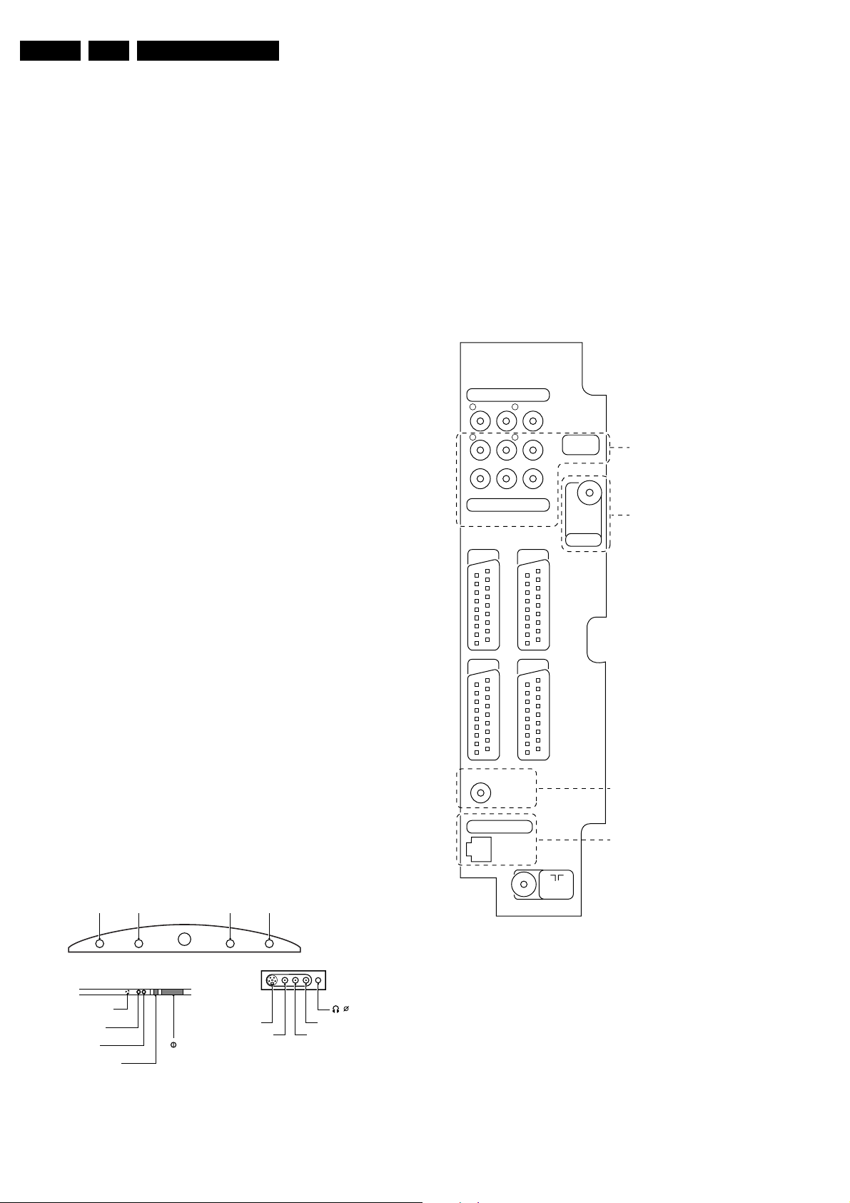
1.2 Connections
1.2.1 Front, top control and Side I/O Connections
TOP CONTROL
-+
FRONT VIEW
IR RECEIVER
BLUE LED
RED LED
LIGHT SENSOR
M
SK 1
-+
P/CHVOLUME
SIDE I/O
SVHS
VIDEO
3.5
AUDIO R
AUDIO L
CL 36532008_015.eps
060503
EXT.3 EXT.4
SURROUND SOUND
SURROUND SOUND
WIRELESS
TRANSMITTER
TV ANTENNA
75 Ω
CL 26532008_013.eps
SURROUND SOUND
CINCH SOCKET
OR
WIRELESS TR.
SOCKET
070403
Figure 1-2 Rear View
Audio receiver
Audio - Out (Cinch)
R - Audio - R 0.5 Vrms / 1 kohm kq
L - Audio - L 0.5 Vrms / 1 kohm kq
Figure 1-1 Front, top control and Side I/O
Hosiden: SVHS - In
1 - Y Ground H
Audio - In (Cinch)
C - Audio - Centre jq
Page 3
Technical Specifications, Connections, and Chassis Overview
EN 3EM6E 1.
Sets equipped with Surround output for active speakers and Digital Audio:
R - Surround - R 0.5 Vrms / 1 kohm kq
L - Surround - L 0.5 Vrms / 1 kohm kq
- Subwoofer 20 - 250 Hz kq
Digital Audio (if present)
- Dig. audio out kq
- Dig. audio in 2 jq
- Dig. audio in 1 jq
Audio - Out (Cinch)
R - Audio - R 0.5 Vrms / 1 kohm kq
L - Audio - L 0.5 Vrms / 1 kohm kq
FM Radio (Optional)
- IEC-type Coax, 75 ohm D
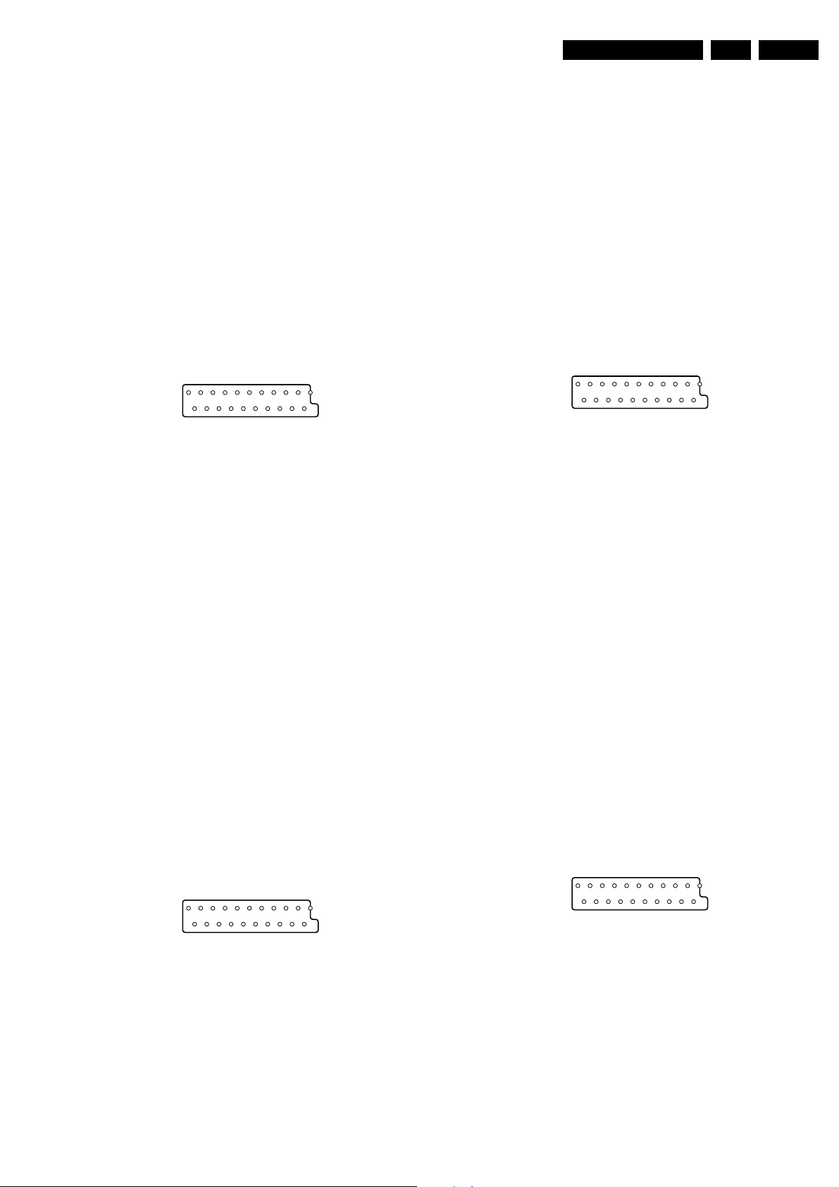
External 1: RGB/YUV and CVBS - In/Out
121
CL96532137_056.eps
202
171199
Figure 1-3 SCART connector
1 - Audio - R 0.5 Vrms / 1 kohm k
2 - Audio - R 0.5 Vrms / 10 kohm j
3 - Audio - L 0.5 Vrms / 1 kohm k
4 - Audio Ground H
5 - Audio Ground H
6 - Audio - L 0.5 Vrms / 10 kohm j
7 - Blue / U 0.7 Vpp / 75 ohm j
8 - CVBS-status 0 - 1.3 V: INT
4.5 - 7 V: EXT 16:9
9.5 - 12 V: EXT 4:3 j
9 - Video Ground H
10 - N.C.
11 - Green / Y 0.7 Vpp / 75 ohm j
12 - N.C.
13 - Video Ground H
14 - Video Ground H
15 - Red / V 0.7 Vpp / 75 ohm j
16 - Status / FBL 0 - 0.4 V: INT
1 - 3 V: EXT / 75 ohm j
17 - Video Ground H
18 - Video Ground H
19 - CVBS-out 1 Vpp / 75 ohm k
20 - CVBS-in 1 Vpp / 75 ohm j
21 - Shielding Ground H
External 2: CVBS and SVHS - In/Out (for VCR)
121
8 - CVBS-status 0 - 1.3 V: INT
4.5 - 7 V: EXT 16:9
9.5 - 12 V: EXT 4:3 j
9 - Video Ground H
10 - Easylink (P50) j
11 - Green 0.7 Vpp / 75 ohm j
12 - N.C.
13 - Video Ground H
14 - Video Ground H
15 - C-in 0.7 Vpp / 75 ohm j
16 - Status / FBL 0 - 0.4 V: INT
1 - 3 V: EXT / 75 ohm j
17 - Video Ground H
18 - Video Ground H
19 - CVBS 1 Vpp / 75 ohm k
20 - CVBS-in 1 Vpp / 75 ohm j
21 - Shielding Ground H
External 3: CVBS - In
121
CL96532137_056.eps
202
171199
Figure 1-5 SCART connector
1 - Ground k
2 - Audio - R 0.5 Vrms / 10 kohm j
3 - Ground k
4 - Audio Ground H
5 - Ground H
6 - Audio - L 0.5 Vrms / 10 kohm j
7 - N.C.
8 - CVBS-status 0 - 1.3 V: INT
4.5 - 7 V: EXT 16:9
9.5 - 12 V: EXT 4:3 j
9 - Video Ground H
10 - N.C.
11 - N.C.
12 - N.C.
13 - Video Ground H
14 - Video Ground H
15 - N.C.
16 - N.C.
17 - Video Ground H
18 - Video Ground H
19 - N.C.
20 - CVBS-in 1 Vpp / 75 ohm j
21 - Shielding Ground H
External 4: CVBS - In
121
CL96532137_056.eps
202
171199
Figure 1-4 SCART connector
1 - Audio - R 0.5 Vrms / 1 kohm k
2 - Audio - R 0.5 Vrms / 10 kohm j
3 - Audio - L 0.5 Vrms / 1 kohm k
4 - Audio Ground H
5 - Audio Ground H
6 - Audio - L 0.5 Vrms / 10 kohm j
7 - C-out 0.7 Vpp / 75 ohm k
CL96532137_056.eps
202
171199
Figure 1-6 SCART connector
1 - Ground k
2 - Audio - R 0.5 Vrms / 10 kohm j
3 - Ground k
4 - Audio Ground H
5 - Ground H
6 - Audio - L 0.5 Vrms / 10 kohm j
7 - N.C.
8 - CVBS-status 0 - 1.3 V: INT
4.5 - 7 V: EXT 16:9
9.5 - 12 V: EXT 4:3 j
Page 4
EN 4 EM6E1.
Technical Specifications, Connections, and Chassis Overview
9 - Video Ground H
10 - N.C.
11 - N.C.
12 - N.C.
13 - Video Ground H
14 - Video Ground H
15 - N.C.
16 - N.C.
17 - Video Ground H
18 - Video Ground H
19 - N.C.
20 - CVBS-in 1 Vpp / 75 ohm j
21 - Shielding Ground H
1.3 Chassis Overview
CRT PANEL
F
Surround - Sound
Sets equipped with Surround-Out jack plug 3,5 mm
- Surround
Audio 0.2 - 2 Vrms / 10 kohm ok
Sets equipped with Wireless Transmitter: RJ45
1 - SDA_TM Signal jk
2 - SCL_TM Signal k
3 - GND Ground H
4 - GND Ground H
5 - 11V_S Supply k
6 - AUDIO_SL 2.8 Vrms k
7 - GND AUDIO Ground H
8 - AUDIO_SR 2.8 Vrms k
Aerial - In
- IEC-type Coax, 75 ohm D
TOP CONTROL PANEL
P
P
SIDE I/O PANEL
O
SMALL SIGNAL BOARD
B
SCAVEM PANEL
SC
Figure 1-7 PWB location
MAINSWITCH PANEL
HDR MODULE BOARD
TIME SHIFT INTERFACE BOARD
HARD DISC
LARGE SIGNAL PANEL
DC-SHIFT (optional)
DAF PANEL
CL 36532008_183.eps
E
HR
TS
A
G
I
061103
Page 5
Safety and Maintenance Instructions, Warnings, and Notes
2. Safety and Maintenance Instructions, Warnings, and Notes
EN 5EM6E 2.
2.1 Safety Instructions
Safety regulations require that during a repair:
• Due to the chassis concept, a very large part of the circuitry
(incl. deflection) is 'hot'. Therefore, connect the set to the
mains via an isolation transformer.
• Replace safety components, indicated by the symbol h,
only by components identical to the original ones. Any
other component substitution (other than original type) may
increase risk of fire or electrical shock hazard.
• Wear safety goggles when you replace the CRT.
Safety regulations require that after a repair, you must return
the set in its original condition. Pay, in particular, attention to
the following points:
• General repair instruction: as a strict precaution, we advise
you to re-solder the solder connections through which the
horizontal deflection current is flowing. In particular this is
valid for the:
1. Pins of the line output transformer (LOT).
2. Fly-back capacitor(s).
3. S-correction capacitor(s).
4. Line output transistor.
5. Pins of the connector with wires to the deflection coil.
6. Other components through which the deflection current
flows.
Note: This re-soldering is advised to prevent bad connections
due to metal fatigue in solder connections, and is therefore only
necessary for television sets more than two years old.
• Route the wire trees and EHT cable correctly and secure
them with the mounted cable clamps.
• Check the insulation of the mains cord for external
damage.
• Check the strain relief of the mains cord for proper function,
to prevent the cord from touching the CRT, hot
components, or heat sinks.
• Check the electrical DC resistance between the mains plug
and the secondary side (only for sets that have an isolated
power supply). Do this as follows:
1. Unplug the mains cord and connect a wire between the
two pins of the mains plug.
2. Turn on the main power switch (keep the mains cord
unplugged!).
3. Measure the resistance value between the pins of the
mains plug and the metal shielding of the tuner or the
aerial connection of the set. The reading should be
between 4.5 MΩ and 12 MΩ.
4. Switch the TV 'off' and remove the wire between the
two pins of the mains plug.
• Check the cabinet for defects, to prevent the possibility of
the customer touching any internal parts.
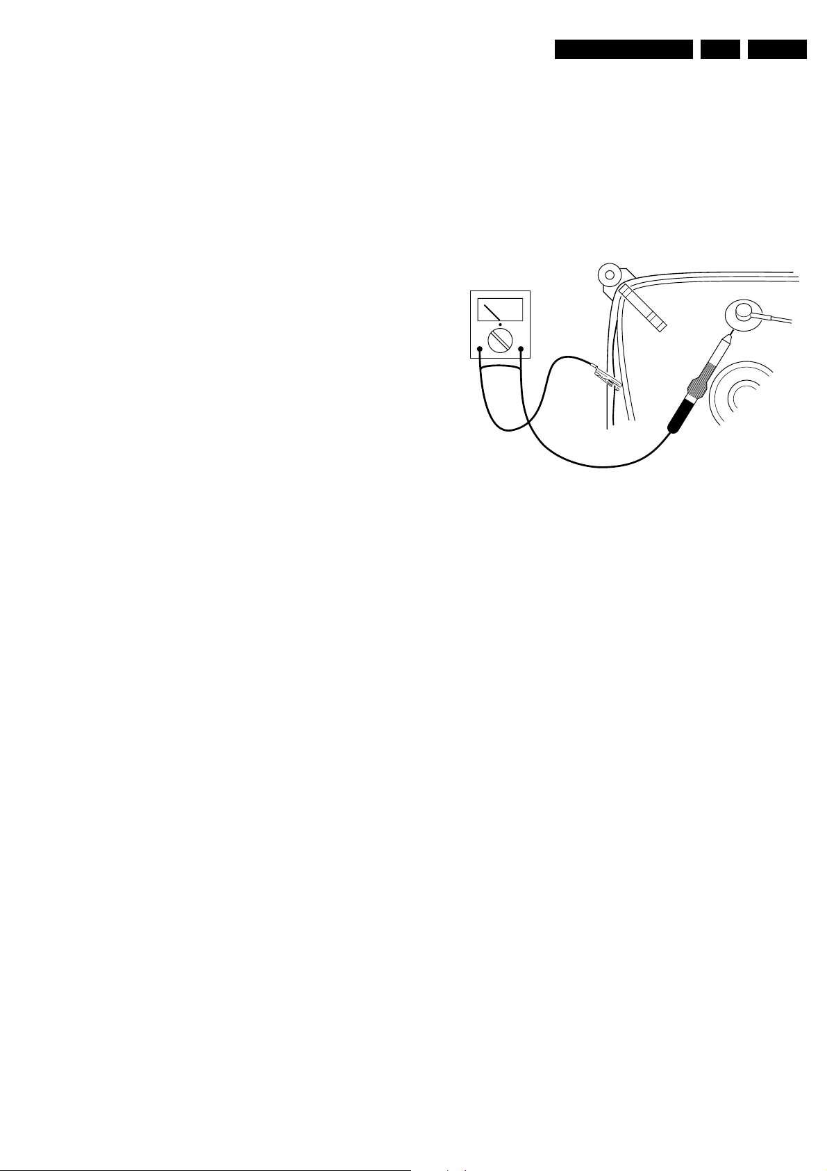
2.3 Warnings
• In order to prevent damage to ICs and transistors, avoid all
high voltage flashovers. In order to prevent damage to the
picture tube, use the method shown in Fig. 2-1, to
discharge the picture tube. Use a high voltage probe and a
multi-meter (position V
reading is 0 V (after approx. 30 s).
V
Figure 2-1 Discharge picture tube
• All ICs and many other semiconductors are susceptible to
electrostatic discharges (ESD, symbol w). Careless
handling during repair can reduce life drastically. Make
sure that, during repair, you are connected with the same
potential as the mass of the set by a wristband with
resistance. Keep components and tools also at this
potential. Available ESD protection equipment:
– Complete kit ESD3 (small tablemat, wristband,
connection box, extension cable and ground cable)
4822 310 10671.
– Wristband tester 4822 344 13999.
• Together with the deflection unit and any multi-pole unit,
flat square picture tubes form an integrated unit. The
deflection and the multi-pole units are set optimally at the
factory. We do not recommend adjusting this unit during
repair.
• Be careful during measurements in the high voltage
section and on the picture tube.
• Never replace modules or other components while the unit
is 'on’.
• When you align the set, use plastic rather than metal tools.
This will prevent any short circuits and the danger of a
circuit becoming unstable.
). Discharge until the meter
DC
CL96532156_040.eps
140501
2.2 Maintenance Instructions
We recommend a maintenance inspection carried out by
qualified service personnel. The interval depends on the usage
conditions:
• When a customer uses the set under normal
circumstances, for example in a living room, the
recommended interval is three to five years.
• When a customer uses the set in an environment with
higher dust, grease, or moisture levels, for example in a
kitchen, the recommended interval is one year.
• The maintenance inspection includes the following actions:
1. Perform the 'general repair instruction' noted above.
2. Clean the power supply and deflection circuitry on the
chassis.
3. Clean the picture tube panel and the neck of the picture
tube.
These values are indicated by means of the appropriate symbols.
2.4 Notes
2.4.1 General
• Measure the voltages and waveforms with regard to the
chassis (= tuner) ground (symbol H), or hot ground (symbol
I), depending on the tested area of circuitry.
• The voltages and waveforms shown in the diagrams are
indicative. Measure them in the Service Default Mode (see
chapter 5) with a colour bar signal and stereo sound (L: 3
kHz, R: 1 kHz unless stated otherwise) and picture carrier
at 475.25 MHz (PAL) or 61.25 MHz (NTSC, channel 3).
• Where necessary, measure the waveforms and voltages
with (symbol D) and without (symbol E) aerial signal.
Measure the voltages in the power supply section both in
normal operation (symbol G) and in standby (symbol F).
Page 6

EN 6 EM6E2.
Safety and Maintenance Instructions, Warnings, and Notes
• The picture tube panel has printed spark gaps. Each spark
gap is connected between an electrode of the picture tube
and the Aquadag coating.
• The semiconductors indicated in the circuit diagram and in
the parts lists, are interchangeable per position with the
semiconductors in the unit, irrespective of the type
indication on these semiconductors.
• Manufactured under license from Dolby Laboratories.
‘Dolby’, ‘Pro Logic’ and the ‘double-D symbol’, are
trademarks of Dolby Laboratories.
Figure 2-2 Dolby PL Symbol
2.4.2 Schematic Notes
• All resistor values are in ohms and the value multiplier is
often used to indicate the decimal point location (e.g. 2K2
indicates 2.2 kOhm).
• Resistor values with no multiplier may be indicated with
either an 'E' or an 'R' (e.g. 220E or 220R indicates 220
Ohm).
• All Capacitor values are expressed in Micro-Farads (µ=
-6
x10
), Nano-Farads (n= x10-9), or Pico-Farads (p= x10
• Capacitor values may also use the value multiplier as the
decimal point indication (e.g. 2p2 indicates 2.2 pF).
• An 'asterisk' (*) indicates component usage varies. Refer to
the diversity tables for the correct values.
• The correct component values are listed in the Electrical
Replacement Parts List. Therefore, always check this list
when there is any doubt.
-12
aligned under a microscope or magnifying glass. If this is not
possible, try to align the (LF)BGA with any board markers.
To reflow the solder, apply a temperature profile according to
the IC data sheet. So as not to damage neighbouring
components, it may be necessary to reduce some
temperatures and times.
).
2.4.3 Rework on BGA ICs (Ball Grid Array)
General
Although (LF)BGA assembly yields are very high, there may
still be a requirement for component rework. By rework, we
mean the process of removing the component from the PWB
and replacing it with a new component. If an (LF)BGA is
removed from a PWB, the solder balls of the component are
deformed drastically so the removed (LF)BGA has to be
discarded.
Device removal
As is the case with any component, it is essential when
removing an (LF)BGA that the board, tracks, solder lands, or
surrounding components are not damaged. To remove an
(LF)BGA, the board must be uniformly heated to a temperature
close to the reflow soldering temperature. A uniform
temperature reduces the chance of warping the PWB.
To do this, we recommend that the board is heated until it is
certain that all the joints are molten. Then carefully pull the
component off the board with a vacuum nozzle. For the
appropriate temperature profiles, see the IC data sheet.
Area preparation
When the component has been removed, the vacant IC area
must be cleaned before replacing the (LF)BGA.
Removing an IC often leaves varying amounts of solder on the
mounting lands. This excessive solder can be removed with
either a solder sucker or solder wick. The remaining flux can be
removed with a brush and cleaning agent.
After the board is properly cleaned and inspected, apply flux on
the solder lands and on the connection balls of the (LF)BGA.
Note: Do not apply solder paste, as this has shown to result in
problems during re-soldering.
Device replacement
The last step in the repair process is to solder the new
component on the board. Ideally, the (LF)BGA should be
Page 7
3. Directions for Use
Directions for Use
EN 7EM6E 3.
Page 8
EN 8 EM6E3.
Directions for Use
Page 9
Directions for Use
EN 9EM6E 3.
Page 10
EN 10 EM6E3.
Directions for Use
Page 11

Directions for Use
EN 11EM6E 3.
Page 12
EN 12 EM6E3.
Directions for Use
Page 13
Directions for Use
EN 13EM6E 3.
Page 14
EN 14 EM6E3.
Directions for Use
Page 15
Directions for Use
EN 15EM6E 3.
Page 16
EN 16 EM6E3.
Directions for Use
Page 17
Directions for Use
EN 17EM6E 3.
Page 18
EN 18 EM6E3.
Directions for Use
Page 19
Directions for Use
EN 19EM6E 3.
Page 20
EN 20 EM6E3.
4
B
b
¬
+
-
V
+
-
P
v
b
i
0
h
q
Select
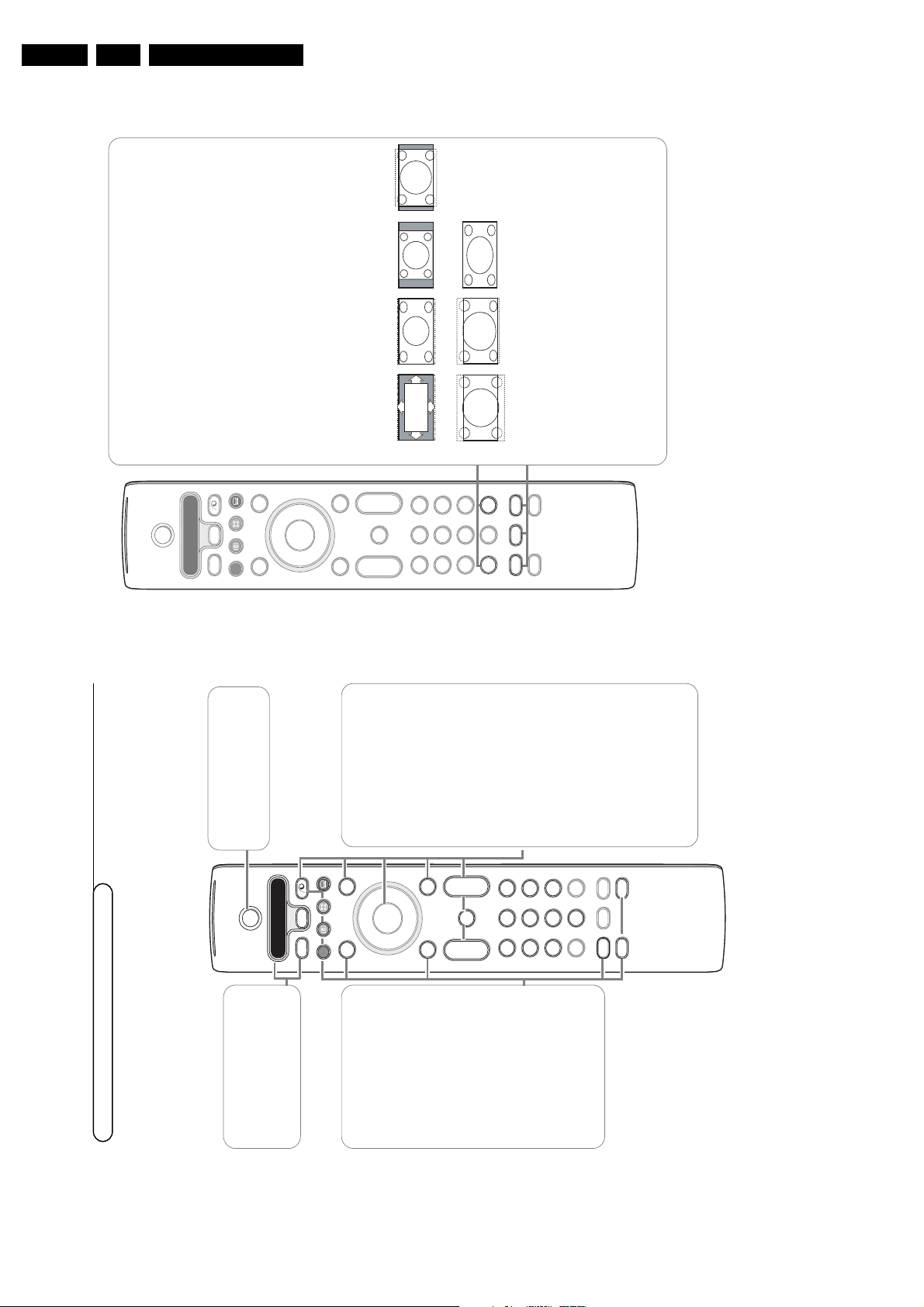
VCR DVD SAT AMP CD
MENU
DVR
OK
123
456
789
0
Ò
®
‡π
†
Active Control
æ
Ò
†
Ï
Pause Live
REC
i On Screen information
Press to display information about the selected TV channel and
programme.
Menu/Remote control info
When a menu is on screen, press
i
to display info on the selected
menu item. For information on the remote control functions, while the
menu info is displayed,press any key on the remote control.
The normal function of the key is not executed.
0 Smart surf /
NEX
TV
IEW
themes
With this key you can easily switch between 2 up to 9 different TV
channels or sources or quickly select TV programmes if
NEX
TV
IEW
with
defined themes is broadcast. See General, Smart surf, p. 8.
Press the
OK
key or wait for the time out to dismiss the Smart surf
display.
b Dual screen / PIP / Multipip
See p. 8 and p. 14
h
Active control see p. 11
q Picture format
Press this key repeatedly or press the cursor up/down to select another
picture format:Auto format, Super zoom, 4:3, Movie Expand 14:9, Movie
Expand 16:9, Subtitle zoom or Wide screen.
Auto format makes the picture fill the screen as much as possible.
In case of subtitles in the bottom black bar,Auto format makes the
subtitles visible. If subtitles are only partly visible, press cursor up.
In case of a broadcaster logo in the corner of the top black bar, the logo
disappears from the screen.
Super zoom removes the black bars on the sides of 4:3 programs with
negligible distortion.
When in Movie Expand 14:9, 16:9,Super zoom or Subtitle zoom picture
format, you can make subtitles visible with the cursor up/down.
Auto format Super zoom 4:3 Movie Expand 14:9
Movie Expand 16:9 Subtitle zoom Wide screen
33
B
b
¬
+
-
V
+
-
P
v
b
i
0
h
q
Select
VCR DVD SAT AMP CD
MENU
DVR
OK
123
456
789
0
Ò
®
‡π
†
Active Control
æ
Ò
†
Ï
Pause Live
REC
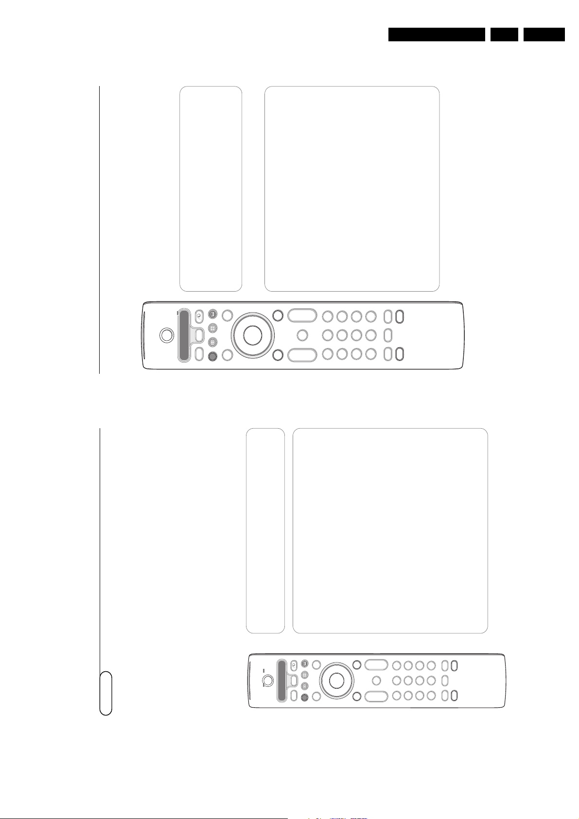
Use of the remote control RC4303
B Standby
Press to switch the TV on or off.
When switched off, a red
indicator on the TV lights up.
®Ò‡π†
Audio- and Video equipment keys
p. 25
REC / DVR / PAUSE / LIVE
Flex TV functions, see p. 19
U Time display
The time is displayed on the
screen.
Q Surround mode
Press this key repeatedly to
select another available surround
mode.
Ì Cinema Go
See separate Cinema Link
booklet supplied.
æ
NEX
TV
IEW
on/off p. 15
Press the
b
key to show
NEX
TV
IEW
/ Teletext Guide on the
right half of the screen.
VCR DVD SAT AMP CD
Audio- and Video equipment keys
(p. 25)
v Select peripherals
(p. 24)
x
Pixel Plus demo on/off
In the right part Pixel Plus and
Digital Natural Motion are
switched on.
b Teletext
on/off p. 17
Press the
b
key to show
teletext on the right half of the
screen.
OK
Press this key
• to activate your choice, when in
the menus.
• to display the programme list.
Ï
Main menu on/off see p. 5VTo adjust the volume.¬Interrupt the sound or restore it.
P Programme selection
To browse through the TV
channels and sources stored in
the favourite list.
0/9 Digit keys
To select a TV channel.
For a two digit programme
number,enter the second digit
before the dash disappears.To
switch immediately to a selected
one digit TV channel, keep the
digit key pressed a bit longer.
Note: For most keys pressing a key once will activate the function. Pressing a second time will de-activate it.
When a key enables multiple options, a small list will be shown.Press repeatedly to select the next item in the list.
The list will be removed automatically after 4 seconds or press
OK
to remove immediately.
Directions for Use
Page 21
Directions for Use
20
B
b
¬
+
-
V
+
-
P
v
b
i
0
h
q
Select
VCR DVD SAT AMP CD
MENU
DVR
OK
123
456
789
0
Ò
®
‡π
†
Active Control
æ
Ò
†
Ï
Pause Live
REC
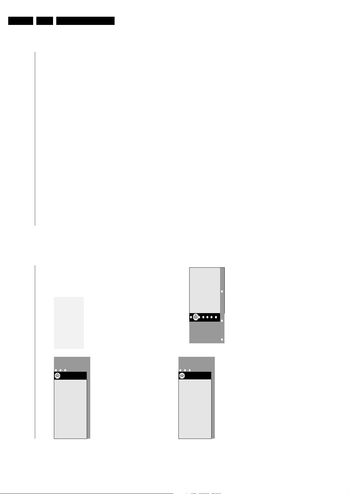
Fast forward and backward
&
Press the Pause key to continue watching the programme from the point
where you paused.
é
Press the cursor right or left (for at least 1 second).
The TV switches to a higher speed of viewing in the forward or backward
direction.“Sequential cursor right or left actions will increase the speed to the next
step (x2, x4,x8, x 20, x 200).‘When viewing at a higher speed than normal in the forward or backward
direction, cursor right or left will bring the speed one step down or up.(Press the Pause key to return to normal speed.
Instant Skip
Press the cursor right shortly,when continuing watching.
Each instant press will skip 30 seconds of the programme, e.g.
commercials.
Instant Replay
At any moment in time, you can press the cursor left to review the
previous 7 seconds once.
Note: Fast forward or backward, Instant skip and Instant replay are not possible from
a programme in a paused state.
Slow Motion
&
Press the cursor right when the programme is paused.
The TV switches to slow motion at a quarter of the normal speed.
é
Press the cursor right again.The TV switches to slow motion at half the
normal speed.
“
Press the Pause key to switch off slow motion.
1919
B
b
¬
+
-
V
+
-
P
v
b
i
0
h
q
Select
VCR DVD SAT AMP CD
MENU
DVR
OK
123
456
789
0
Ò
®
‡π
†
Active Control
æ
Ò
†
Ï
Pause Live
REC
REC
Instant recording
p. 22
Press to start a direct recording of the programme which is being
displayed.
DVR
Table of Recordings and Programmed recording
See p. 21
PAUSE TV
&
Press the Pause key.
The picture will freeze while the TV keeps recording the live TV
programme in the background.
(The memory block is defined at 3 hours HQ - High Quality- recording.)
A time bar and a time indication show the growing delay from the real
time live programme as the pause continues.
Press the
i
key to display the bar once again after it disappeared.
é
Press the Pause key again to continue watching the programme from the
point where you paused, without missing a part.
LIVE TV
Press the Live key to jump back to regular TV viewing.
Press again to return to the paused moment.
PAUSE CLEAR
In case you might not want to share the programmes you have been
watching (the evening) before, and which have been automatically
recorded ( in the 3 hours memory block), you may consider to empty
the memory.&Press the
MENU
Ï
key.
é
Select Pause clear in the Features menu. See TV menu,Features, p. 13“Press the
OK
key to erase the 3 hours memory block.
Your Flex TV has an internal memory capacity to store programmes temporarily (
Pause TV
) and to
record programmes for an indefinite time (
Recording
).
1. Pause TV
: From the moment your TV is switched on, in the background it automatically records the
programme you are watching.This gives you the opportunity to interrupt watching (with the
Pause
key) and to progress the viewing (by pressing the
Pause
key again) at a later time (max. 3 hours
later) without missing a single part of the programme.This is called Pause TV.
Note:When the Pause TV memory block (3 hours) is full, the background recording continues overwriting the
programmes recorded earlier.
2. Recording
: A greater part of the memory of the Flex TV is reserved to record programmes you
want to keep (with a max. of 58 programmes and with a total max. recording time of appr. 28
hours).You may execute instant recordings with the ®
Instant record
key or programme your
recordings with the
DVR
key. See further on.
Notes:
- You may already start viewing before the recording is complete.
- When an instant or programmed recording has started, Pause TV is not possible at the same time.
- Flex TV functionality is not possible in Dual screen/PIP/Multipip.
Flex TV
EN 21EM6E 3.
Page 22
EN 22 EM6E3.
22
Instant recording
&
Press the
REC
key.
The recording starts immediately and a small
menu pops up where you have to enter the
duration time of the recording you want to
do.The default duration is set at 01.00 hour
but can be changed at any time.
é
Press the cursor right and enter the duration
time of the recording with the digit keys or
with the cursor up/down.
Press the
OK
key to confirm and press the
REC
key again to remove the menu.
Note:
- Once the recording started, you may switch your
TV to standby or watch another programme.
DO NOT Power off your TV or else the recording
may be lost.
- See Table of Recordings how to modifiy the
programme name (Record xxx) automatically
filled in.
“
To stop the recording before the entered
duration time, press the
REC
key, select
Stop
and press the
OK
key.
To change the duration time, press the
REC
key, and use the cursor keys to change the
duration time. Press the
OK
key to confirm
and press the
REC
key again to remove the
menu.
Modifying the record quality of Instant
recording
The recording duration depends on the
record quality you choose in the General
Setup menu, p. 8, to record in.
Do not change the HQ quality default setting
for the highest picture quality.
Record quality Flex TV
•
HQ
(High Quality) recording quality (approx.
6 hours) can be compared with DVD.
•
SQ
(Standard Quality) with a quality still
better than VHS but a longer record duration
(approx. 11 hours).
•
LP
(Long Play) (approx.28 hours).
General remarks on Flex TV
- While a recording is in progress, and when a lock becomes active, the recording is stopped and you are
summoned to enter your code.
- The audio reproduction for Instant or Programmed Recording is always mono.
- The total number of already recorded ( in the Over view menu) + programmed ( in the Scheduled record menu)
recordings is limited to 58 programmes ( although there is still time space left).When the total number is
reached, first delete some recordings to create place for new ones.
- Pay attention not to programme overlapping recordings or recordings which start at the same time.
- When there is no free memor y left, the oldest recorded programme is automatically erased and without any
warning.
- Once an Instant or Programmed Recording has started, you can start watching the programme while
the recording continues. Select the programme in the Overview menu.
To stop the recording while you are watching, first press the
LIVE
key on the remote control.Then
press the
REC
key and select Stop on the Recording menu on screen.
- Once the recording is set or has started, there is no need for the TV to remain on.You can switch the TV to
standby and the recording will happen in standby. DO NOT power off your TV.
- You can easily transfer recorded programmes to a DVD recorder or VCR,connected to
EXT 2
.
Select the programme in the Overview menu and select
Play
. You record what you are watching on the screen.
- To stop an already started Programmed Record (before the entered stop time): press the
REC
key on the
remote control and select Stop on the Recording menu on screen.
- All Flex TV featuring is not applicable on copyright protected programmes and on programmes coming from
peripheral equipment connected to
EXTERNAL 2
.
- To pause a NTSC transmission:
Select a NTSC programme and first clear the memory block with
Pause clear
in the Features menu.Then
press the
Pause
key.
To pause a PAL or SECAM transmission again:
Select the new programme and clear the memory block again.Then press the
Pause
key.
21
Table of Recordings
&
Press the
DVR
key.
This menu allows you to
• view a list of programmes stored in the
memory (
Overview
);
• view a list of programmed recordings
(
Scheduled record
):
• set a programmed recording (
Set record
).
Each recording is listed with the date of
recording, the picture quality (
HQ, SQ
or
LP
)
with which the recording has been done, the
duration and the title of the recording.
In the
Overview
menu it is indicated how
much free memory space is left. Each
programme can be played (
Play
) or deleted
(
Delete
) from this menu.The title of a
programme can be modified (
Modify
) using a
virtual keyboard on screen.
é
Press the corresponding green colour key on
the remote control to select the
Scheduled
record
list.
“
Select
Add
to bring up the Programmed
record menu and to add a new programme
(See also Programmed Record),
Modify
to
change a programmed recording,
Delete
to
delete a programmed recording.
‘
Press the the red colour key to return to the
Overview
list or the yellow colour key to
select
Set record
. (See Programmed record.)
To modify a programme title with the virtual
keyboard
The virtual keyboard appears on the screen if you
have decided to modify a programme title.
&
Press the cursor left/right, up/down to select the
characters, words or functions.éPress the
OK
key to confirm each character
selected.
“
Select
Cancel
to cancel the modification;
Space
to
enter a space;
Delete
to delete the last character
selected;
Shift
to switch between undercast or
capital characters;
Special
to display special
characters on the keyboard and press the
OK
key.
‘
Select
Accept
to confirm the modified title.
Programmed Record
&
Press the
DVR
key.
é
Press the corresponding green colour key on
the remote control to select the
Scheduled
record
list.
“
Press the yellow colour key in the Scheduled
Record menu to select
Set Record
to
programme a recording.
‘
Use the cursor up/down, left/right to select and
to enter the channel to record from, the date,
the start and stop time, the title of the
programme and the recording quality.
Remark: in order to avoid non-existing start or stop
time indications, it may happen that you have to
modify the second digit first before entering or
changing the first digit.(Select
Store
and press
OK
to confirm the
recording data.
Overview
Overview Scheduled record Set record
TUE 14 JAN HQ 120m Meet Joe Black
SUN 19 JAN SQ 140m Star Wars 3
SAT 08 FEB LP 240m Olympic opening
THU 13 FEB HQ 50m Miami Vice
FRI 15 MAR HQ 120m Manu vs Paris
SAT 07 APR SQ 30m Friends
MON 10 APR LP 25m Naked chef
Space Left LP 10.20h
P
P
lay
lay
Modify
Modify
Delete
Delete
Overview
Overview Scheduled record Set record
CANVA TUE 15 APR 15.37-16.37 Pauli
BBC1 SUN 27 APR 19.37-20.37 Naked chef
FOCUS SAT 03 MAY 16.25-16.55 Friends
BBC2 THU 08 MAY 20.18-20.45 Vicar
MERID FRI 23 MAY 21.15-22.10 No win
Add
Modify
Modify
Delete
Delete
® Cancel ® Accept
® Space ® Delete
ABCDEFG 1 23
HIJKLMN 4 56
OPQRSTU 7 89
VWXYZ 0
® Shift ® Special
02 BBC
Men In black
Tue 21 Aug
20.30
22.00
HQ
Channel
Title
Date
Start Time
Stop Time
Quality
Store
Overview
Overview Scheduled record Set record
Directions for Use
Page 23
4. Mechanical Instructions
Mechanical Instructions
EN 23EM6E 4.
Index of this chapter:
1. Set Disassembly
2. Service Positions
3. Assy / PWB Removal
4. Set Re-assembly
Notes:
• Figures below can deviate slightly from the actual situation,
due to the different set executions.
• Follow the disassemble instructions in described order.
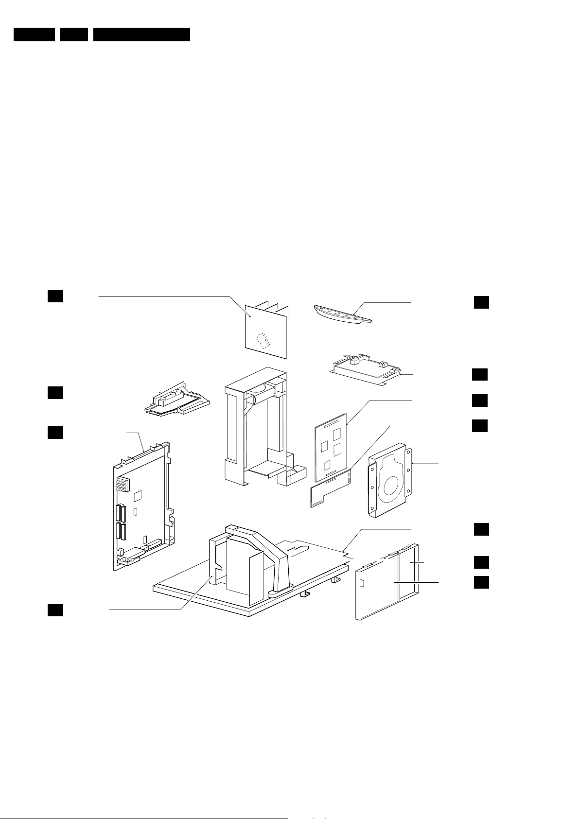
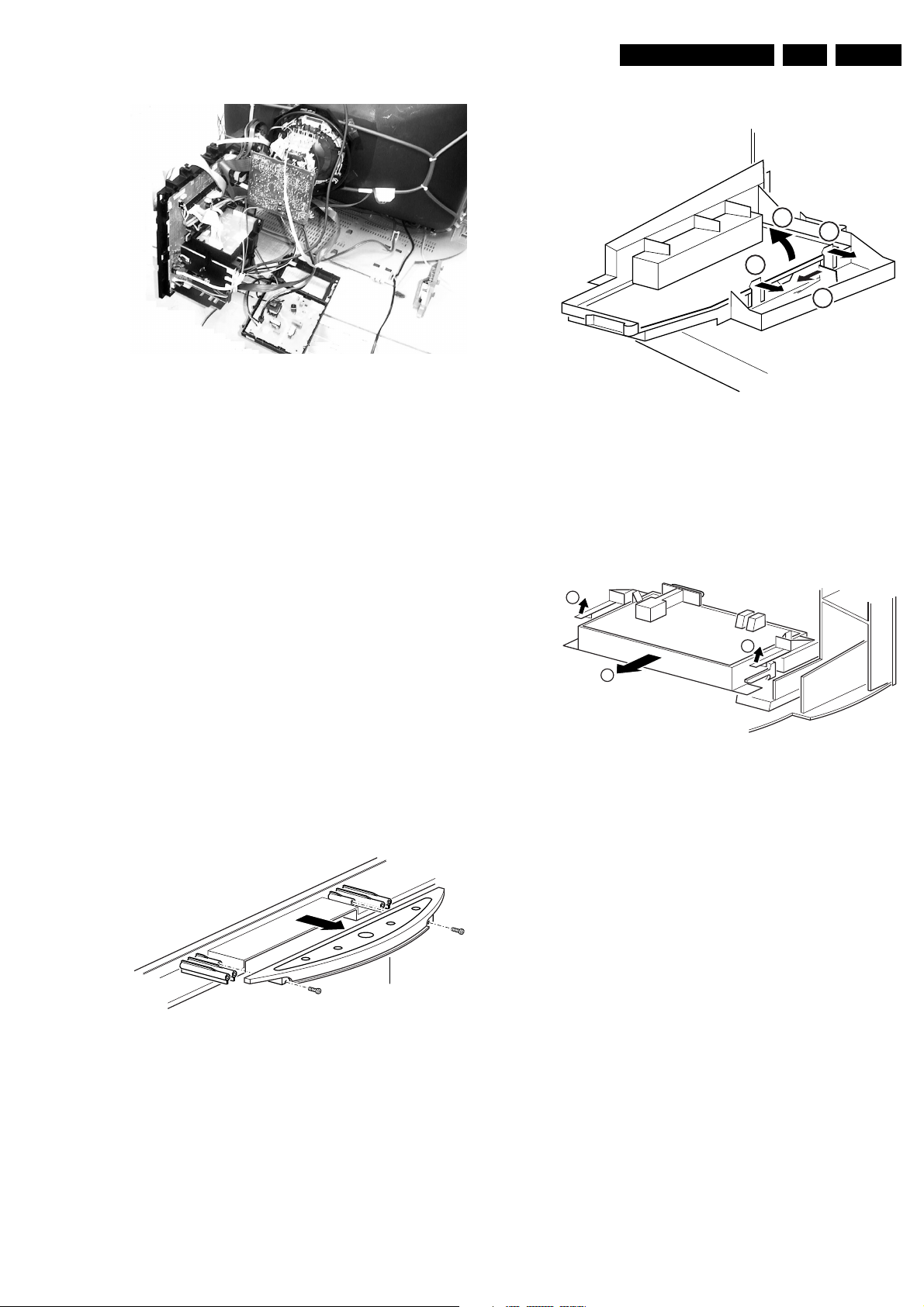
4.1 Set Disassembly
4.1.1 Wireless Surround Transmitter Removal (if attached)
1. Remove the cable of the Wireless Surround Transmitter
box (at the right side of this RJ45 plug you can find the
release-hook of the lock-mechanism).
2. Pull the Wireless Surround Transmitter box backwards. It
is clicked to the rear cover via three clamps.
4.1.2 Rear Cover Removal
1
2 (5x)
3
1. Disconnect the loudspeaker cable connectors at the top of
the sub-woofer box.
2. Unlock he subwoofer bracket and at the same time pull the
unit backwards.
3. Take out the sub-woofer unit including the bracket.
4.2 Service positions
4.2.1 DAF Module
1
2
4
4
3
3
CL 16532044_011.eps
Figure 4-2 DAF module
1. Remove the fixation screw (if present) as described in
section: ‘Assy/PWB removal’.
2. Push down the fixation clamp, and pull the complete
bracket at the same time loose from the LSP bracket. The
module is now unlocked from the chassis and can be
handled in several positions.
3
4.2.2 Small Signal Board and Hard Disk Recorder Module
150501
SERVICE CONNECTOR
CL 36532008_009.eps
Figure 4-1 Removal of the rear cover
Warning: Disconnect the mains power cord before you remove
the rear cover.
First, unscrew the top cover plate:
1. Remove the fixation screw(s) [1] that secure the cover
plate.
2. Remove the top cover plate and the rear cover screws,
hidden by this top cover plate.
To be able to access the electronics of the set, you must
remove the rear cover:
1. Disconnect all communication cables.
2. Remove the fixation screws [2] of the rear I/O cover plate.
3. Remove the remaining fixation screws [3] of the rear cover.
4. Unlock the securing clips at bottom side and remove the
rear cover. Make sure not to damage any cable during this
cover removal.
4.1.3 Sub-woofer Removal
Caution: Do not disconnect the loudspeaker cable from the
subwoofer box when the set is operative, because the class-D
amplifier cannot handle a change in load during operation.
It is no problem when the subwoofer is disconnected before
operation, but a change from connected to disconnected
during operation can damage the amplifier.
040403
Small Signal Board (SSB) Bracket Removal
1. Unlock the SSB bracket at the position, as shown at the
figure, and pull out the SSB bracket.
CL 26532008_014.eps
040403
Figure 4-3 SSB bracket removal
Place the SSB bracket in a service position as shown at the
figure.
Page 24
EN 24 EM6E4.
Mechanical Instructions
4.2.3 LSP Component side
2
1
FAN
CL 36532008_186.eps
141103
Figure 4-4 SSB bracket in a service position
Hard Disk Recorder (HDR) Bracket Removal
1. Unscrew the two mounting screws (1), if available.
2. Unplug the cable from the connector 1100 and 1101.
3. Pull up the two fixation clamps (2) and pull the bracket one-
two cm in direction of the set, to release two clamps at the
left side of the bracket.
4. Take the HDR bracket out.
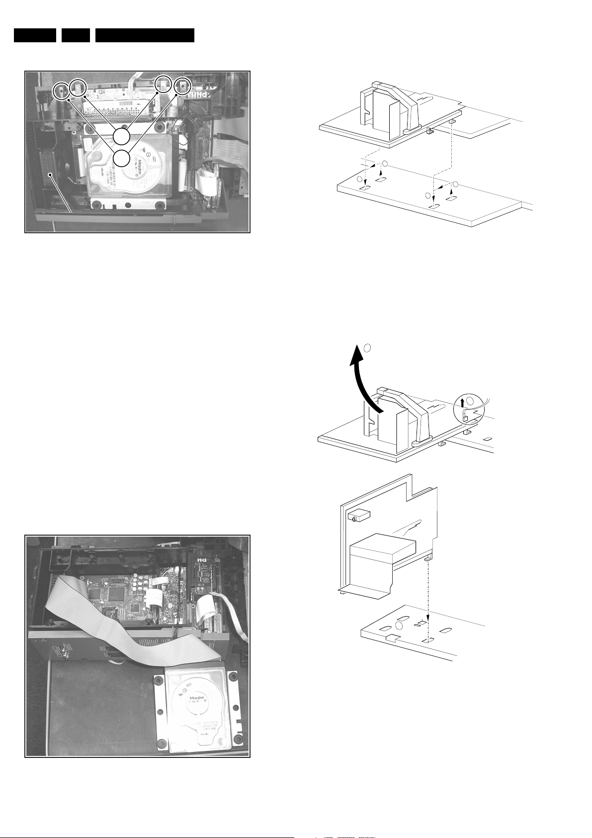
Hard Disk Removal
1. Unscrew all screws from the metal cover shield of the HDR
module. Take out the cover shield, releasing the two
clamps at the its left side.
2. Unplug all cables from the Hard disk.
3. Lift and remove the Hard disk.
4. Caution: Handle the hard disc with care; the mechanics of
a hard disc are very sensitive, even a slight knock can
affect the data on the disc.
Note: For measurements replace the IDE flat cable, which
connects Hard disk with SSB, by ‘IDE extended flat cable’, 48
cm, 40 fold (ordering code for one cable: 3104 311 05501).
Alternatively, use the cable from the service extension tool
9965 000 14526.
1
2
1
2
Figure 4-6 LSP unlock action
1. Make sure the SSB bracket is unlocked and placed on the
table.
2. Release the LSP bracket locking clips and pull it out of the
mounting holes.
4.2.4 Solder Side LSP
2
1
1502
CL 36532008_010.eps
040403
CL 36532008_185.eps
Figure 4-5 Hard disk in a service position
061103
3
CL 36532008_011.eps
Figure 4-7 Place LSP in Service position
040403
Page 25
Mechanical Instructions
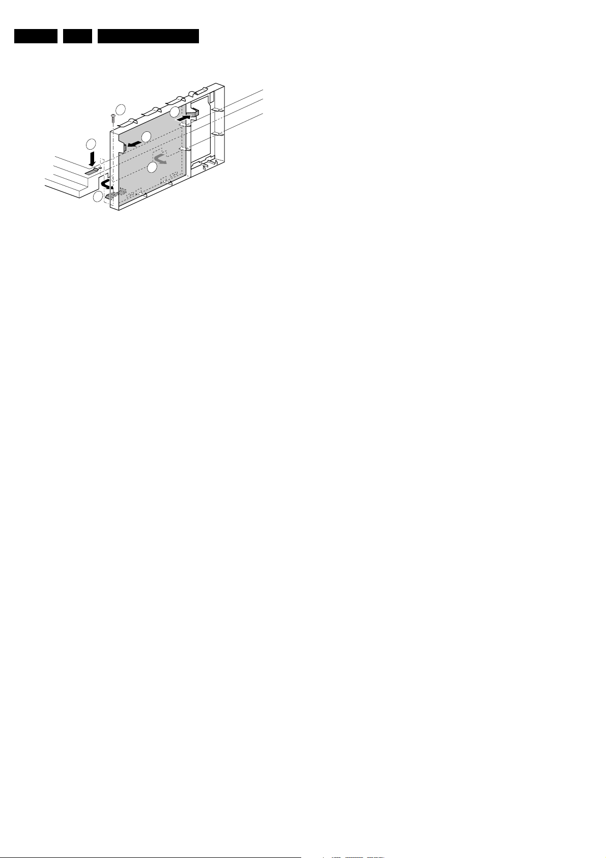
4.3.2 Side-I/O Assy / Panel
EN 25EM6E 4.
CL 36532008_017.eps
070503
Figure 4-8 Service position LSP
For better accessibility of the LSP, do the following (see also
figure above):
1. Make sure the DAF module is uncoupled from the LSP
bracket.
2. Unlock both LSP fixation clamps and pull it backwards to
release it out of the mounting holes.
3. To disconnect the degaussing coil from the LSP, remove
the cable from connector 1502 [1].
4. Release the wiring from their fixation clamps, in order to get
room for repositioning the LSP.
5. Replace the IDE flat cables by two ‘IDE extended flat
cables’, 48 cm, 40 fold (ordering code for one cable: 3104
311 05501). Or use the cables from the service extension
tool 9965 000 14526.
6. Rotate the LSP 90 degrees clockwise [2], and place it in
one of the bottom fixation holes as shown in the figure.
7. Hook the bracket in the first row of fixation holes of the
bottom tray, see figure.
3
2
Figure 4-10 Side I/O assy
1. Release the snap-hook [1] with your finger.
2. At the same time, pull the assy backwards.
3. Release the two fixation clamps on the right side of the
bracket [2] (the board hinges at the left side).
4. Remove the board from the bracket.
4.3.3 Mains Switch Assy / Panel
1
1
2
2
1
CL 16532149_069.eps
061201
4.3 Assy / PWB Removal
Sometimes, it can be necessary to swap a complete assy or
Printed Wiring Board (PWB). How that can be done is
explained below.
4.3.1 Top Control Assy / Panel
Top control board
Figure 4-9 Top control assy
1. Release both fixation screws about five full turns.
2. Pull the complete assy back- and upwards (it hinges in the
cabinet front).
3. Flip the assy, and you can access the board by releasing
(carefully) the four fixation clamps.
CL 16532149_068.eps
051201
CL 16532149_070.eps
061201
Figure 4-11 Mains Switch Assy
1. Release the two fixation clamps by pushing them upwards
[1]. At the same time, pull the complete assy backwards [2].
Note: be aware that the degaussing coil/cable can hamper
this.
2. Release the two fixation clamps on the two sides of the
bracket (the board hinges at the connector side).
3. Remove the board from the bracket.
4. When the light guide (located in the cabinet, in front of the
LEDs) is defective, you can replace it by pushing it
forwards at the left side (it hinges at the right side, seen
from the rear).
Page 26
EN 26 EM6E4.
4.3.4 DAF Assy / Panel
Mechanical Instructions
1
2
4
4
3
3
CL 16532044_011.eps
Figure 4-12 DAF-module
1. Remove the fixation screw [1] (if the screw is present).
2. Disconnect the cables.
3. Push down the fixation clamp [2], and pull the complete
bracket at the same time backwards. The module is now
unlocked from the LSP bracket and can be removed.
4. Release the PWB fixation clamps [4], to remove the print
from the DAF bracket.
4.3.5 Auto-Scavem Assy / Panel
This panel is mounted in a bracket on the left side of the LSP.
It is not necessary to remove the bracket.
1. Release the two PWB fixation clamps at top as well as at
bottom side of the PWB.
2. Remove the cables
3. Take out the Auto-Scavem PWB.
150501
4.3.6 Small Signal Board (SSB)
1. Unlock the bracket and at the same time pull the bracket
out of the locking holes.
2. Place the SSB bracket on the table.
3. To remove the PWB disconnect the cables, unscrew the
mounting screws and take the PWB out of its bracket.
4.3.7 Large Signal Panel (LSP)
1. Unlock the LSP bracket as described in section "Service
positions".
2. Disconnect the necessary cables.
3. Remove the PWB mounting screws and release the
fixation clamps on the left of the LSP-bracket (the board
hinges at the right side).
4. Remove the board from the bracket.
4.4 Set Re-assembly
To reassemble the whole set, do all processes in reverse order.
Be sure that, before the rear cover is mounted:
• The mains cord is mounted correctly in its guiding brackets.
• All wires/cables are returned in their original positions. This
is very important due to the large "hot" area of the set
Page 27

Service Modes, Error Codes, and Fault Finding
5. Service Modes, Error Codes, and Fault Finding
EN 27EM6E 5.
Index of this chapter:
1. Test points
2. Service Modes
3. Problems and solving tips (related to CSM)
4. ComPair
5. Error Codes
6. The blinking LED procedure
7. Protections
8. Repair tips
9. Software downloading
5.1 Test Points
The chassis is equipped with test points printed on the circuit
board assemblies. They refer to the diagram letters.
Perform measurements under the following conditions:
• Service Default Mode.
• Video: colour bar signal.
• Audio: 3 kHz left, 1 kHz right.
5.2 Service Modes
Service Default Mode (SDM) and Service Alignment Mode
(SAM) offer several features for the service technician, while
the Customer Service Mode (CSM) is used for communication
between a Philips Customer Care Centre (P3C) and a
customer.
There is also the option of using ComPair, a hardware interface
between a computer (see requirements below) and the TV
chassis. It offers the ability of structured troubleshooting, test
pattern generation, error code reading, software version
readout, and software upgrading.
Minimum requirements: a Pentium processor, Windows 95/
98, and a CD-ROM drive (see also paragraph “ComPair”).
Note: In this chassis, the bi-coloured LED (red/green) is
replaced by two separate LEDs, a blue and a red one. The blue
LED is controlled by software (via ON_OFF_LED). The red
LED will light in anti-phase to the blue, but with a time delay.
This means that if the blue LED is blinking fast, the red LED will
stay off, but after the blue LED is “OFF” long enough, the red
LED will go “ON”.
So take care: In certain service modes (e.g. blinking LED,
stepwise start-up, etc.) you must observe the blue LED and
ignore the red LED.
5.2.1 Service Default Mode (SDM)
Purpose
• To create a pre-defined setting, to get the same
measurement results as given in this manual.
• To override SW protections.
• To start the blinking LED procedure.
Specifications
• Tuning frequency: 475.25 MHz for PAL/SECAM.
• Colour system: SECAM L for France or PAL B/G for the
rest of Europe.
• All picture settings at 50 % (brightness, colour, contrast).
• All sound settings at 50 %, except volume at 25 %.
• All service-unfriendly modes (if present) are disabled, like:
– (Sleep) timer.
– Child/parental lock.
– Blue mute.
– Automatic volume limiter (AVL).
– Auto switch-off (when no video signal was received for
10 minutes).
– Skip/blank of non-favourite pre-sets.
– Smart modes.
– Auto store of personal presets.
– Auto user menu time-out.
How to enter SDM
Use one of the following methods:
• Use the standard RC-transmitter and key in the code
“062596”, directly followed by the “MENU” button.
Note: It is possible that, together with the SDM, the main
menu will appear. To switch it off, push the “MENU” button
again.
• Short for a moment the two solder pads on SSP print, with
the indication “SDM”. These solder pads are present at
both sides of the print. Activation can be performed in all
modes, except when the set has a problem with the mainprocessor.
Caution: If the SDM is entered via the pins, all the
software-controlled protections are de-activated.
• Use the DST-emulation feature of ComPair.
• Use the “DEFAULT” button on the Dealer Service Tool
(RC7150).
After entering this mode, “SDM” will appear in the upper right
corner of the screen.
How to navigate
When you press the “MENU” button on the RC transmitter, the
set will toggle between the SDM and the normal user menu
(with the SDM mode still active in the background).
How to exit SDM
Use one of the following methods:
• Switch the set to STANDBY via the RC-transmitter.
• Press the “EXIT” button on the DST.
• Via a standard customer RC-transmitter: key in “00”-
sequence.
5.2.2 Service Alignment Mode (SAM)
Purpose
• To perform (software) alignments.
• To change option settings.
• To easily identify the used software version.
• To view operation hours.
• To display (or clear) the error code buffer.
Specifications
• Operation hours counter.
• Software version.
• Option settings.
• Error buffer reading and erasing.
• Software alignments.
How to enter SAM
Use one of the following methods:
• Via a standard RC transmitter: key in the code “062596”
directly followed by the “OSD [i+]” button. After entering
SAM with this method a service warning will appear on the
screen, you can continue by pressing any digit key on the
RC.
• Short for a moment the two solder pads on SSP print, with
the indication SAM. These solder pads are present at both
sides of the print. Depending on the software version it is
possible that the service warning will appear, you can
continue by pressing any digit key on the RC.
• Use the DST-emulation feature of ComPair.
• Press the ALIGN button on the DST while the set is in the
normal operation
Page 28
EN 28 EM6E5.
Service Modes, Error Codes, and Fault Finding
After entering this mode, “SAM” will appear in the upper right
corner of the screen.
Contents of SAM:
• OPERATION HOURS. Displays the accumulated total of
operation hours (not the standby hours).
• HARDWARE INFO
– ROM VERSION. Displays the date of the software and
the software version of the ROM (example: EM6EU1-
1.0_01234 = AAABBC-X.Y_NNNNN).
• AAA= the chassis name.
• BB= the region: EU= Europe, AP= Asia Pacific
PAL/Multi, AN= Asia Pacific NTSC, US= USA, LT=
LATAM.
• C= the language cluster number.
• X.Y= the software version, where X is the main
version number (different numbers are not
compatible with one another) and Y is the sub
version number (a higher number is always
compatible with a lower number).
• NNNNN= last five digits of 12nc code software.
– SW VERSION RDS RADIO. Displays the software
version of the RDS radio (if RDS radio is present).
• ERRORS (followed by maximal 10 errors). The most
recent error is displayed at the upper left (for an error
explanation see paragraph “Error Codes”).
• DEFECTIVE MODULE. Here the module that generates
the error is displayed. If there are multiple errors in the
buffer, which are not all generated by a single module,
there is probably another defect. It will then display the
message “UNKNOWN” here.
• RESET ERROR BUFFER. When you press the “OK”
button, the error buffer is reset.
• ALIGNMENTS. This will activate the “ALIGNMENTS” sub-
menu.
• DEALER OPTIONS. Extra features for the dealers.
• SERVICE OPTIONS. Extra features for Service.
• INITIALISE NVM. When an NVM was corrupted (or
replaced) in the former EM3 chassis, the microprocessor
replaces the content with default data (to assure that the
set can operate). However, all pre-sets and alignment
values are gone now, and option numbers are not correct.
Therefore, this was a very drastic way. In this chassis, the
procedure is implemented in another way: The moment the
processor recognises a corrupted NVM, the “initialise
NVM” line will be highlighted. Now, you can do two things
(dependent of the service instructions at that moment):
– Save the content of the NVM via ComPair for
development analysis, before initialising. This will give
the Philips Service department an extra possibility for
diagnosis (e.g. when Development asks for this).
– Initialise the NVM (same as in the past, however now it
happens conscious).
• STORE. All options and alignments are stored when
pressing the “OK”-button
• FUNCTIONAL TEST. All devices are tested via the “OK”
button. Eventual errors are displayed in the error buffer.
The error buffer is not erased, the content returns when this
test is terminated.
• DAILY MENUS. With the “OK” button, you can go to the
normal user menu. SAM is still active in the background.
With the “MENU” button, you return from the user menu to
SAM menu. This feature can be helpful to quickly change
some settings in the user menu.
• SW MAINTENANCE
• UPGRADE. More info see paragraph Software
downloading.
• EVENTS. Not useful for service purposes. In case of
specific software problems, the development
department can ask for this info.
• BDM INFO. Broadcast Debug Menu info. The purpose
of this menu is to debug the broadcast, not the TV. The
menu gives an overview of what is received on the
current preset. Following items are displayed:
P r e s e t n r : -- UTC: - - : - - : --
P r e s e t n a m e : ----- LTO: - - : - - : --
Time: - - : - - : --
C N I N V M : ---- Date: - - / - - / ----
C N I F 1 : ----
C N I F 2 : ---- Time TXT: - - : - - : --
C N I V P S : ---- Time 8/30 F1: - - : - - : --
M o r n i n g P r o g : --- Date 8/30 F1: - - / - - / ----
N a m e 8 / 3 0 F 1 : ----- LTO 8/30 F1: - - : - - : --
N a m e 8 / 3 0 F 2 : -----
N a m e T X T : ----- WSS G1: - - - -
S i g n a l S t r e n g t h :--- WSS G2: - - - -
WSS G3: - - -
E P G S e r v i c e : --- WSS G4: - - -
CL 36532017_055.eps
240403
Figure 5-1 Broadcast debug menu overview.
Table 5-1 Broadcast debug menu explanation
Item Source Description
Presetnr Set Presetnumber of the current
selected preset.
Presetname Set Presetname of the current
selected preset.
CNI NVM Broadcaster CNI number stored in NVM for
the current preset.
CNI F1 Broadcaster CNI number from transmitted
Packet 8/30 Format 1.
CNI F2 Broadcaster CNI number from transmitted
Packet 8/30 Format 2.
CNI VPS Broadcaster CNI number from transmitted
VPS line.
Morning Prog Broadcaster "ARD" or "ZDF" according to
dedicated bit in 8/30 Format 1.
Name 8/30 F1 Broadcaster Name extracted from status
message of 8/30 Format 1.
Name 8/30 F2 Broadcaster Name extracted from status
message of 8/30 Format 2.
Name TXT Broadcaster Name extracted from TXT
header.
Signal
Strength
FBX Noise figure measured for
selected preset.
EPG Service Set EPG Service stored in NVM for
current preset displayed as
"TXT", "MCP", "SCP", "OCP".
UTC Set UTC (Universal Time Code
formerly known as Greenwich
Mean Time) used in the set.
LTO Set LTO (Local Time Offset) used
in the set. Used by EPG for all
Nextview displays. (= Time
TXT header - Time 8/30 F1 )
Time Set Current time running in the set.
Was extracted at startup, then
maintained by software.
Date Set Current date running in the set.
Was extracted at startup, then
maintained by software.
Time TXT Broadcaster TXT header time from the
selected preset.
Time 8/30 F1 Broadcaster UTC time from 8/30 Format 1.
Date 8/30 F1 Broadcaster Date from 8/30 Format 1.
LTO 8/30 F1 Broadcaster LTO from 8/30 Format 1.
WSS G1 Broadcaster WSS Group 1 (Aspect Ratio)
bits 0 1 2 3
WSS G2 Broadcaster WSS Group 2 (Enhanced
Services) bits 4 5 6 7
WSS G3 Broadcaster WSS Group 3 (Subtitles) bits 8
9 10
WSS G4 Broadcaster WSS Group 4 (Reserved) bits
11 12 13
Page 29

Service Modes, Error Codes, and Fault Finding
EN 29EM6E 5.
How to navigate
• In SAM, you can select the menu items with the “CURSOR
UP/DOWN” key on the RC-transmitter. The selected item
will be highlighted. When not all menu items fit on the
screen, move the “CURSOR UP/DOWN” key to display the
next/previous menu items.
• With the “CURSOR LEFT/RIGHT” keys, it is possible to:
– (De) activate the selected menu item.
– Change the value of the selected menu item.
– Activate the selected submenu.
How to exit SAM
Use one of the following methods:
• Press the “MENU” button on the RC-transmitter, or
• Switch the set to STANDBY via the RC-transmitter, or
• Press the “EXIT” button on the DST.
5.2.3 Customer Service Mode (CSM)
Purpose
When a customer is having problems with his TV-set, he can
call his dealer. The service technician can than ask the
customer to activate the CSM, in order to identify the status of
the set. Now, the service technician can judge the severity of
the complaint. In many cases, he can advise the customer how
to solve the problem, or he can decide if it is necessary to visit
the customer.
The CSM is a read only mode; therefore, modifications in this
mode are not possible.
How to enter CSM
Use one of the following methods:
• Press the “MUTE” button on the RC-transmitter
simultaneously with the “MENU” button on the TV (top
control) for at least 4 seconds.
• Key in the code “123654” via the standard RC transmitter.
Note: Activation of the CSM is only possible if there is no (user)
menu on the screen!
How to navigate
By means of the “CURSOR-DOWN/UP” knob on the RCtransmitter, you can navigate through the menus.
Contents of CSM
Customer Service Menu 1
• SOFTWARE VERSION (example: EM6EU1-1.0_01234).
Displays the built-in software version. In case of field
problems related to software, software can be upgraded
(for more details, see paragraph Software downloading).
You will find details of the software versions in the chapter
“Software Survey” of the “Product Survey - Colour
Television” publication. This publication is generated four
times a year.
• FEATURE BOX. The 12NC-number of the built-in Feature
Box software
• SET TYPE. This information is very helpful for a helpdesk/
workshop as reference for further diagnosis. In this way, it
is not necessary for the customer to look at the rear of the
TV-set.
• CODE 1. Gives the latest 5 errors of the error buffer. As
soon as the built-in diagnose software has detected an
error the buffer is adapted. The last occurred error is
displayed on the leftmost position. Each error code is
displayed as a 3-digit number. When less than 10 errors
occur, the rest of the buffer is empty (000). See also
paragraph Error Codes for a description.
• CODE 2. Gives the first 5 errors of the error buffer. See
also paragraph Error Codes for a description.
• VOLUME. Gives the last status of the volume as set by the
customer. The value can vary from 0 (volume is minimum)
to 100 (volume is maximum). Volume values can be
changed via the volume key on the RC-transmitter.
• BRIGHTNESS. Gives the last status of the brightness as
set by the customer. The value can vary from 0 (brightness
is minimum) to 100 (brightness is maximum). Brightness
values can be changed via the “CURSOR LEFT” and
“CURSOR RIGHT” keys on the RC-transmitter after
pressing the “MENU” button and selecting “PICTURE” and
“BRIGHTNESS”.
• CONTRAST. Gives the last status of the contrast as set by
the customer. The value can vary from 0 (contrast is
minimum) to 100 (contrast is maximum). Contrast values
can be changed via “CURSOR LEFT” and “CURSOR
RIGHT” keys on the RC-transmitter after pressing the
“MENU” button and selecting “PICTURE” and
“CONTRAST”.
• COLOUR. Gives the last status of the colour saturation, as
set by the customer. The value can vary from 0 (colour is
minimum) to 100 (colour is maximum). Colour values can
be changed via “CURSOR LEFT” and “CURSOR RIGHT”
keys on the RC-transmitter after pressing the “MENU”
button and selecting “PICTURE” and “COLOUR”.
• HUE. Only relevant for NTSC-signals (e.g. some NTSC-
DVD-discs).
Customer Service Menu 2
• SHARPNESS. Gives the sharpness value. The value can
vary from 0 (sharpness is minimum) to 7 (sharpness is
maximum). In case of bad antenna signals, a too high
value of the sharpness can result in a noisy picture.
Sharpness values can be changed via the “CURSOR
LEFT” and “CURSOR RIGHT” keys on the RC-transmitter
after pressing the “MENU” button and selecting “PICTURE”
and “SHARPNESS”.
• HEADPHONE VOLUME. Gives the last status of the
headphone volume, as set by the customer. The value can
vary from 0 (volume is minimum) to 100 (volume is
maximum). Headphone volume values can be changed via
the “CURSOR LEFT” and “CURSOR RIGHT” keys on the
RC-transmitter after pressing the “MENU” button and
selecting “SOUND” and “HEADPHONE VOLUME”.
• DOLBY. Indicates whether the received transmitter
transmits Dolby sound (“ON”) or not (“OFF”). Attention: The
presence of Dolby can only be tested by the software on
the Dolby Signaling bit. If a Dolby transmission is received
without a Dolby Signaling bit, this indicator will show “OFF”
even though a Dolby transmission is received.
• SURROUND MODE. Indicates the by the customer
selected surround mode (or automatically chosen mode).
In case the set is a Non-Dolby set, there will be displayed
“0”. If it is a Dolby-set then is displayed: “STEREO”, “3
STEREO”, “HALL”, “3DSURROUND”, “DOLBY PRO
LOGIC” or “DOLBY DIGITAL”. These settings can be
influenced after pressing the “MENU” button and selecting
“SOUND” and SURROUND MODE”. It can also have been
selected automatically by signaling bits (internal software).
• TUNER FREQUENCY. Indicates the frequency the
selected transmitter is tuned to. The tuner frequency can
be changed via the “CURSOR LEFT” and “CURSOR
RIGHT” keys for fine tune after opening the installation
menu and selecting “INSTALL” and “MANUAL INSTALL”.
• DIGITAL OPTION. Gives the selected digital mode, “100
HZ”, “DIGITAL SCAN”, “NATURAL MOTION”, “DOUBLE
LINES”, or “PIXEL PLUS”. Change via “MENU”,
“PICTURE”, “DIGITAL OPTIONS”.
• CENTRE TRIM. Indicates the difference between main
volume and volume of centre speaker. Change via:
“MENU”, “SETUP”, “SPEAKERS”, and “CENTRE
VOLUME” (not available when “Surround Mode” is set to
“STEREO” or “HALL”). The value can vary from “-10” to
“+10”
• TV SYSTEM. Gives information about the video system of
the selected transmitter.
– BG: PAL BG signal received.
– DK: PAL DK signal received.
Page 30

EN 30 EM6E5.
Service Modes, Error Codes, and Fault Finding
– I: PAL I signal received.
– L/La: SECAM L/La signals received.
– M: NTSC M signal received with video carrier on 38.9
MHz.
Customer Service Menu 3
• BALANCE. Indicates the balance settings, between “-50”
and “+50”. Change via “MENU”, “SOUND”, and
“BALANCE”. Not applicable for Dolby Pro Logic sets.
• CENTRE MODE. Indicates if centre mode is set “ON” or
“OFF”. When centre mode is on, all TV speakers are used
as one centre speaker. Change Centre mode via “MENU”,
“SETUP”, “SPEAKERS”, and “CENTRE MODE”.
• DNR. Gives the selected DNR setting (Dynamic Noise
Reduction), “OFF”, “MINIMUM”, “MEDIUM”, or
“MAXIMUM”. Change via “MENU”, “PICTURE”, “DNR”
• NOISE FIGURE. Gives the noise ratio for the selected
transmitter. This value can vary from 0 (good signal) to 127
(average signal) and to 255 (bad signal). For some
software versions, the noise figure will only be valid when
“Active Control” is set to “medium” or “maximum”.
• SOURCE. Indicates which source is used and the video/
audio signal quality of the selected source. (Example:
Tuner, Video/NICAM) Source: “TUNER”, “EXT1”, “EXT2”,
“EXT3”, “EXT4”, “SIDE”, “AV1”, “AV2”, “AV3” or “AV4”.
Video signal quality: “VIDEO”, “S-VIDEO”, “RGB 1FH”,
“YPBPR 1FH 480P”, “YPBPR 1FH 576P”, “YPBPR 1FH
1080I”, “YPBPR 2FH 480P”, “YPBPR 2FH 576P”, “YPBPR
2FH 1080I”, “RGB 2FH 480P”, “RGB 2FH 576P” or “RGB
2FH 1080I”. Audio signal quality: “STEREO”, “SPDIF 1”,
“SPDIF 2” or “SPDIF”.
• AUDIO SYSTEM. Gives information about the audio
system of the selected transmitter: “ANALOGUE MONO”,
“ANALOGUE STEREO”, “PCM 2/0”, “DD 1/0”, “DD 2/0
LtRt”, “DD 2/0 L0R0”, “DD 2/1”, “DD 2/2”, “DD 3/0”, “DD 3/
1”, “DD 3/2”, “DD 1+1”, “MPEG 1/0”, “MPEG 2/0”, “MPEG
2/0 LtRt”, “MPEG 2/1”, “MPEG 2/2”, “MPEG 3/0”, “MPEG
3/1”, “MPEG 3/2”, “MPEG 1+1” or “MPEG 2+2”.
• TUNED BIT. Gives information about the tuning method of
the stored pre-set. If a channel is found via “automatic
installation”, you will see the value “Yes”. When you
change this (automatically found) frequency via “fine tune”
adjustment (installation menu - manual installation), the
displayed value will change to “No”. Therefore, when you
see the value “No” in this line, it is an indication that the
received channel is a non-standard signal (e.g. of a VCR).
• SURROUND SPEAKERS. Indicates if the surround
speakers are present, “YES” or “NO”. Change via “MENU”,
“SETUP”, “SPEAKERS”, and “SURROUND SPEAKERS”.
• ON TIMER. Indicates if the “On Timer” is set “ON” or “OFF”
and if the timer is “ON” also displays start time, start day
and program number. Change via “MENU”, “TV”,
“FEATURES”, and “ON TIMER”.
• PRESET LOCK. Indicates if the selected preset has a child
lock: “LOCKED” or “UNLOCKED”. Change via “MENU”,
“TV”, “FEATURES”, “CHILD LOCK”, and “CUSTOM
LOCK”.
Customer Service Menu 4
• CHILD LOCK. Indicates the last status of the general child
lock: “UNLOCK”, “LOCK”, or “CUSTOM LOCK”. Change
via “MENU”, “TV”, “FEATURES”, “CHILD LOCK”, and
“LOCK”.
• AGE LOCK. Indicates the last status of the EPG rating for
child lock: “OFF”, “4 YEARS”, “6 YEARS”, “8 YEARS”, “10
YEARS”, “12 YEARS”, “14 YEARS” or “16 YEARS”. This is
only displayed if child lock is set to “CUSTOM LOCK”
• LOCK AFTER. Indicates at what time the child lock is set:
“OFF” or e.g. “18:45” (lock time). This is only displayed if
child lock is set to “CUSTOM LOCK”
• CATEGORY LOCK. Indicates the last status of the EPG
theme childlock: “MOVIES”, “NEWS”, “SHOWS”,
“SPORTS”, “CHILDREN”, “MUSIC”, “CULTURE”, or
“SERIES”. This is only displayed if child lock is set to
“CUSTOM LOCK”. It is possible that more than one value
is shown.
• PROGRAM CATEGORY. Indicates the theme of the
selected transmitter: “MOVIES”, “NEWS”, “SHOWS”,
“SPORTS”, “CHILDREN”, “MUSIC”, “CULTURE”, or
“SERIES”.
• TV RATINGS LOCK. Only applicable for US.
• MOVIE RATINGS LOCK. Only applicable for US.
• V-CHIP TV STATUS. Only applicable for US.
Customer Service Menu 5
• V-CHIP MOVIE STATUS. Only applicable for US.
• OPTIONS 1. Gives the option codes of option group 1 as
set in SAM (Service Alignment Mode).
• OPTIONS 2. Gives the option codes of option group 2 as
set in SAM (Service Alignment Mode).
• AVL. Indicates the last status of AVL (Automatic Volume
Level): “ON” or “OFF”. Change via “MENU”, “TV”,
“SOUND”, “AVL”
• DELTA VOLUME. Indicates the last status of the delta
volume for the selected preset as set by the customer: from
“-12” to “+12”. Change via “MENU”, “TV”, “SOUND”,
“DELTA VOLUME”.
• SURROUND TRIM L. Indicates the last status of
“SURROUND LEFT VOLUME” as set by the customer:
from “-10” to “+10”. Only available in Digital Dolby sets.
Change via “MENU”, “SETUP”, “SPEAKERS”,
“SURROUND L VOLUME.
• SURROUND TRIM R. Indicates the last status of
“Surround Right Volume” as set by the customer: from “10” to “+10”. Only available in Digital Dolby sets. Change
via “MENU”, “SETUP”, “SPEAKERS”, “SURROUND R
VOLUME.
• FRONT SPKR DIST. Indicates the last status of the
distance to the front speakers as set by the customer: “1m”,
“2m”, or “3m”,.... Change via “MENU”, “SETUP”,
“SPEAKERS”, “TO FRONT”.
• SURR. SPKR DIST. Indicates the last status of the
distance to the surround speakers as set by the customer:
“1m”, ”2m”, or ”3m”,.... Change via “MENU”, “SETUP”,
“SPEAKERS”, “TO SURROUND”.
Customer Service Menu 5
• TIMESHIFT MODULE. Indicates if communication
between timeshift module and main processor (OTC) is
possible. If communication is possible, “OK” is displayed,
otherwise “NOT RESPONDING” is displayed.
How to exit CSM
Use one of the following methods:
• After you press a key on the RC-transmitter (with exception
of the “CHANNEL”, “VOLUME” and digit (0-9) keys), or
• After you switch the TV-set “OFF” with the mains switch.
5.3 Problems and Solving Tips (related to CSM)
Note: Below described problems are all related to the TV
settings. The procedures to change the value (or status) of the
different settings are described above. New value(s) are
automatically stored.
5.3.1 Picture Problems
Snowy/noisy picture
1. Check line 24 “Noise Figure”. In case the value is 127 or
higher, and the value is also high on other programs, check
the aerial cable/aerial system. For some software versions,
the noise figure will only be valid when “Active Control” is
set to “medium” or “maximum”.
2. Check lines 11 “Sharpness” and 24 “Noise Figure”. In case
the value of line 11 is 3 or 4 and the value of line 24 is high
(127 or higher), decrease the “Sharpness” value.
Page 31

Service Modes, Error Codes, and Fault Finding
EN 31EM6E 5.
Picture too dark
1. Press “MENU”, “TV”, “PICTURE”, “SMART PICTURE”. In
case the picture improves, increase the “Brightness” or the
“Contrast” value. The new value(s) are automatically
stored (in “personal” pre-set) for all TV channels.
2. Check line 7 “Brightness” and 8 “Contrast”. If the value of
line 7 is low (< 10) or the value of line 8 is low (< 10),
increase the “Brightness” or the “Contrast” value.
Picture too bright
1. Press “MENU”, “TV”, “PICTURE”, “SMART PICTURE”. In
case the picture improves, decrease the “Brightness” or the
“Contrast” value. The new value(s) are automatically
stored (in “personal” pre-set) for all TV channels.
2. Check lines 7 “Brightness” and 8 “Contrast”. If the value of
line 7 is high (> 40) or the value of line 8 is high (> 50).
Decrease the “Brightness” value or increase the “Contrast”
value.
White line around picture elements and text
1. Press “MENU”, “TV”, “PICTURE”, “SMART PICTURE”. In
case the picture improves, decrease the “Sharpness”
value. The new value is automatically stored (in “personal”
pre-set) for all TV channels.
2. Check line 11 “Sharpness”. Decrease the “Sharpness”
value. The new value is automatically stored for all TV
channels.
No picture
Check line 27 “Tuned bit”. In case the value is “No”, install the
required program again. Open the installation menu and
perform manual installation.
Blue picture
No proper signal is received. Check the aerial cable/aerial
system.
Blue picture and/or unstable picture
A scrambled or decoded signal is received.
Black and white picture
Check line 9 “Colour”. In case the value is low (< 10), increase
the “Colour” value. The new value is automatically stored for all
TV channels.
No colours/colour lines around picture elements or colours not correct or unstable picture
1. Check line 20 “TV System”. If a “strange” system pops up,
something has gone wrong during installation. Re-install
the channel.
2. In case line 20 is “L”, the installed system for this pre-set is
“France”, while “West Europe” is required. Install the
required program again: open the installation menu and
perform manual installation. Select system “West Europe”.
Menu text not sharp enough
1. Press “MENU”, “TV”, “PICTURE”, “SMART PICTURE”. In
case picture improves, decrease the contrast value. The
new value(s) are automatically stored for all TV channels.
2. Check line 8 “Contrast”. The value of line 8 is high (> 50).
Decrease the contrast value.
5.3.2 Sound Problems
No sound from left and right speaker
Check line 6 “Volume”. The value is low. Increase the value of
“Volume”. The new value(s) are automatically stored (in
“personal” pre-set) for all TV channels.
Sound too loud for left and right speaker
Check line 6 “Volume”. The value is high. Decrease the value
of “Volume”. The new value(s) are automatically stored (in
“personal” pre-set) for all TV channels.
5.4 ComPair
5.4.1 Introduction
ComPair (Computer Aided Repair) is a service tool for Philips
Consumer Electronics products. ComPair is a further
development on the European DST (service remote control),
which allows faster and more accurate diagnostics. ComPair
has three big advantages:
• ComPair helps you to quickly get an understanding on how
to repair the chassis in a short time by guiding you
systematically through the repair procedures.
• ComPair allows very detailed diagnostics (on I
is therefore capable of accurately indicating problem areas.
You do not have to know anything about I
yourself because ComPair takes care of this.
• ComPair speeds up the repair time since it can
automatically communicate with the chassis (when the
microprocessor is working) and all repair information is
directly available. When ComPair is installed together with
the SearchMan electronic manual of the defective chassis,
schematics and PWBs are only a mouse click away.
5.4.2 Specifications
ComPair consists of a Windows based faultfinding program
and an interface box between PC and the (defective) product.
The ComPair interface box is connected to the PC via a serial
or RS232 cable.
For this chassis, the ComPair interface box and the TV
communicate via a bi-directional service cable via the service
connector.
The ComPair faultfinding program is able to determine the
problem of the defective television. ComPair can gather
diagnostic information in two ways:
• Automatic (by communication with the television):
ComPair can automatically read out the contents of the
entire error buffer. Diagnosis is done on I
can access the I
and receive I
television. In this way, it is possible for ComPair to
communicate (read and write) to devices on the I
of the TV-set.
• Manually (by asking questions to you): Automatic
diagnosis is only possible if the micro controller of the
television is working correctly and only to a certain extends.
When this is not the case, ComPair will guide you through
the faultfinding tree by asking you questions (e.g. Does the
screen give a picture? Click on the correct answer: YES /
NO) and showing you examples (e.g. Measure test-point I7
and click on the correct oscillogram you see on the
oscilloscope). You can answer by clicking on a link (e.g.
text or a waveform picture) that will bring you to the next
step in the faultfinding process.
By a combination of automatic diagnostics and an interactive
question / answer procedure, ComPair will enable you to find
most problems in a fast and effective way.
Beside fault finding, ComPair provides some additional
features like:
• Up- or downloading of pre-sets.
• Managing of pre-set lists.
• Emulation of the Dealer Service Tool (DST).
• If both ComPair and SearchMan (Electronic Service
Manual) are installed, all the schematics and the PWBs of
the set are available by clicking on the appropriate
hyperlink. Example: Measure the DC-voltage on capacitor
C2568 (Schematic/Panel) at the Mono-carrier.
– Click on the “Panel” hyperlink to automatically show
the PWB with a highlighted capacitor C2568.
– Click on the “Schematic” hyperlink to automatically
show the position of the highlighted capacitor.
2
C bus of the television. ComPair can send
2
C commands to the micro controller of the
2
C level) and
2
C commands
2
C level. ComPair
2
C busses
Page 32

EN 32 EM6E5.
Service Modes, Error Codes, and Fault Finding
5.4.3 Stepwise Start-up
Under normal circumstances, a fault in the power supply, or an
error during start-up, will switch the television to protection
mode. ComPair can take over the initialisation of the television.
In this way, it is possible to distinguish which part of the startup routine (hence which circuitry) is causing the problem.
In sets with the Muppet IC present (dual screen functionality),
step 2 is skipped.
Take notice that the transition between two steps can take
some time, so give the set some time to reach a stable state.
During the transition time the LED can blink strangely.
Stepwise start- up explanation
This is realised via ComPair and is very helpful when a
protection is activated (see also chapter “Protections”).
Table 5-2 Stepwise start-up table
Display
State Description mode
0 Low power standby: 5V2/3V3
LED
On None
present, uP in standby-mode
1 High power Standby: TV-set
in standby-mode
2 Main Power On: HOP in
standby, 5V/8V present, I2C
Wait 1s,
flash 1 x
Wait 1s,
flash 2 x
protections on, SSB is
powered by standby-supply
(5V/8V). Degaussing (12 s)
has been activated, MSP is
reset.
3 Initialized (Semi standby):
most IC's are initialized, HOP
Wait 1s,
flash 3 x
still in standby
4 HOP: HOP fully powered and
working, EHT is present, rest
Wait 1s,
flash 4 x
of IC's initialized, black
current stabilisation is off,
picture is still blanked
5 On: TV-set operates, black
current stabilisation is on,
Wait 1s,
flash 5 x
picture is unblanked.
Note (*):
• When the set is in stepwise mode and, due to stepping-up,
a protection is activated, the set will really go into protection
(blinking LED). The set will not leave the stepwise-mode
however. If state X is the state where the set went to
protection, stepwise start-up will return to state X-1. At
state (X-1) diagnostic measurements can be performed.
Also, in the short time the set is in state X but not yet in
protection, you can also do some measurements.
• Due to the initialisation process of the Muppet IC, step 2 is
not available in sets with Muppet. In this case, step 2 and
3 become one step
5.4.4 How To Connect
1. First, install the ComPair Browser software (see the Quick
Reference Card for installation instructions).
2. Connect the RS232 interface cable between a free serial
(COM) port of your PC and the PC connector (marked with
“PC”) of the ComPair interface.
3. Connect the mains adapter to the supply connector
(marked with “POWER 9V DC”) of the ComPair interface.
4. Switch the ComPair interface “OFF”.
5. Switch the television set “OFF” with the mains switch.
6. Connect the ComPair interface cable between the
connector on the rear side of the ComPair interface
(marked with “I
2
C”) and the ComPair connector at the rear
side of the TV.
Enabled
protection
None
4 & 5
Plus 1, 6 &
18
Plus 2 & 16
7. Plug the mains adapter in a mains outlet, and switch the
interface “ON”. The green and red LEDs light up together.
The red LED extinguishes after approx. 1 second while the
green LED remains lit.
8. Start the ComPair program and read the “Introduction”
chapter.
EXTERNAL 2
L
R
AUDIO EXTERNAL 1
SERVICE
CONNECTOR
PC VCR I2CPower
9V DC
Figure 5-2 ComPair Interface connection
5.4.5 How To Order
ComPair order codes (EU/AP):
• Starter kit ComPair32/SearchMan32 software and
ComPair interface (excl. transformer): 3122 785 90450.
• ComPair interface (excluding transformer): 4822 727
21631.
• Starter kit ComPair32 software (registration version): 3122
785 60040.
• Starter kit SearchMan32 software: 3122 785 60050.
• ComPair32 CD (update): 3122 785 60110.
• SearchMan32 CD (update): 3122 785 60120.
• ComPair interface cable: 3122 785 90004.
• ComPair firmware upgrade IC: 3122 785 90510.
• Transformer Europe: 4822 727 21632.
• Transformer UK: 4822 727 21633.
5.5 Error Codes
5.5.1 Introduction
The error code buffer contains all detected errors since the last
time the buffer was erased. The buffer is written from left to
right, new errors are logged at the left side, and all other errors
shift one position to the right.
When an error has occurred, the error is added to the list of
errors, provided the list is not full or the error is a protection
error.
When an error occurs and the error buffer is full, then the new
error is not added, and the error buffer stays intact (history is
maintained), except when the error is a protection error.
To prevent that an occasional error stays in the list forever, the
error is removed from the list after 50+ operation hours.
When multiple errors occur (errors occurred within a short time
span), there is a high probability that there is some relation
between them.
5.5.2 How to read the Error Buffer
Use one of the following methods:
• On screen via the SAM (only if you have a picture).
Examples:
– 0 0 0 0 0: No errors detected
– 6 0 0 0 0: Error code 6 is the last and only detected
error
– 9 6 0 0 0: Error code 6 was first detected and error code
9 is the last detected error
CL96532156_029.eps
190600
Page 33

Service Modes, Error Codes, and Fault Finding
EN 33EM6E 5.
• Via the blinking LED procedure (when you have no
picture). See next paragraph.
• Via ComPair.
longer present. Before clearing the buffer, write down the
content, as this history can give you significant information.
If possible, check the entire contents of the error buffer. In
some situations, an error code is only the result of another error
5.5.3 How to clear the Error Buffer
code and not the actual cause (e.g., a fault in the protection
detection circuitry can also lead to a protection).
Use one of the following methods:
• By activation of the “RESET ERROR BUFFER” command
in the SAM menu.
• With a normal RC, key in sequence “MUTE” followed by
“062599” and “OK”.
• When you transmit the commands “DIAGNOSE” - “99” “OK” with ComPair (or with a DST).
• If the content of the error buffer has not changed for 50+
hours, it resets automatically.
5.5.4 Error Codes
There are various errors:
2
• I
C device errors.
2
C bus errors.
• I
• Protection errors.
• Errors not related to an I
– BLACK CURRENT LOOP (ERROR 28): detection of a
continuous fail of the black current stabilisation loop of
the HOP.
– FALCONIC (ERROR 26): at start-up, after initialisation
of the PICNIC, the presence of the FALCONIC can be
checked.
– EAGLE (ERROR 27): at start-up, after initialisation of
the PICNIC, the presence of the Eagle can be
In case of non-intermittent faults, clear the error buffer before
you begin the repair. This to ensure that old error codes are no
checked.
Table 5-3 Error Table
Defect. module
Error Device Description Def. item
indication Diag
1 M24C32 NVM, spontaneous blinking error 1 7011 Control B5a
2 Hfail Protection Horizontal Flyback protection / Horizontal Flyback /
3 SAA4978 PICNIC 7713 Feature Box B3a
4 Supply 5V 5V protection / +5V Supply B5a
5 Supply 8V 8V protection / +8V Supply B5a
6 Slow I2C bus blocked Spontaneous blinking error 6 / Slow I2C Blocked /
7 TDA9330 HOP High-end Output Processor 7301 Video Controller B4
8 TDA932x HIP High-end Input Processor 7323 Chroma IF IO B2
13 UV1318/... Tuner protection 1T01 Tuner B13
14 MSPxxxx ITT sound processor 7A02 Audio module B6a
16 FBX Feature Box Protection / +3V (Fbx) Supply B3
18 Fast I2C bus blocked Spontaneous blinking error 18 / Fast I2C Blocked /
19 TDA8444 Auto Scavem DAC 7500 Auto Scavem SC1
21 M62320P PIP I/O Expander 7P56 Video Dual Screen B15b
23 UV1316/... PIP Tuner 1T02 Video Dual Screen B13
24 SAB9081 PIP Muppet 7PA6 Video Dual Screen B15c
26 SAA4992 Falconic 7718 +3V (Fbx) Supply B3b
27 T8F24EF Eagle 7724 +3V (Fbx) Supply B3c
28 Black current loop Black current loop / /
29 PCF8574T DVD I2C I/O Expander 7306 DVD Engine T3
32 M29W400BT Flash Ram (EPG) 7012 EPG Memory B5a
34 TDA932x Second HIP 7P09 Video Dual Screen B15a
63 MAS3529E Dolby Digital Decoder 7A30 Digital Audio Module B6b
64 SAA6588T TDL RDS 7100 TDL (Radio) T2
81 DPL4519 Dolby Prologic Decoder 7A63 Digital Audio Module B6c
82 TDA7309D Headphone processor 7A06 B6a
83 TEA6422 (1) Source select matrix audio 7I17 Audio Source Select B14d
84 TEA6422 (2) Source select matrix audio 7I18 Audio Source Select B14d
85 TEA6415 Source select matrix video 7I24 Video Source Select B14a
86 P89C664 TDL P Radio 7002 TDL (Radio) T1
87 / TDL 12V audio off / TDL (Radio) T1
88 TEA5762 TDL FM Radio 7101 TDL (Radio) radio
89 M24C32 TDL NVM Radio 7011 TDL (Radio) T1
91 See extra info TDL LCD / TDL (Radio) T
92 See extra info TDL Motor / TDL (Radio) T
93 See extra info DVD 3V3 / DVD Engine T3
96 PCF8574 HDD Interface 7022 Harddisk Module TS
97 See extra info HDD Engine / Harddisk Module /
98 See extra info HDD Fan fan Harddisk Module TS
2
C device, but of importance:
Page 34

EN 34 EM6E5.
Service Modes, Error Codes, and Fault Finding
Note:
• Error codes 1, 6, or 18 are protection codes and in this
case, supplies of some circuits will be switched “OFF”.
Also, in protection, the LED will blink the number of times
equivalent to the most recent error code.
• Some errors are only for TDL-sets (EM6E AB) or sets with
hard disk.
Extra info for certain errors:
• Error 91: If the TDL microprocessor gets an error from the
LCD display, this will be reported to the OTC, and will log
error 91 (only for TDL sets).
• Error 92: If one of the micro-switches of the LCD display is
not closed within a timeout, the TDL microprocessor will
report an error to the OTC, and error 92 will be logged (only
for TDL sets).
• Error 93: If the 3V3 is not present in DVD mode, or is
present when DVD is in stand-by, error 93 will be logged.
The presence or absence of the supply voltage is detected
via the I/O expander (schematic T3) (only for TDL sets).
• Error 97: There are 2 inputs to generate an error: The IO
expander that checks the supply voltages and the HDD
processor witch controls the hard disk itself. Both generate
the same error: HDD error (only for sets with HDD).
• Error 98: via a control line of the HDD interface IC (7022)
is sensed if the HDD fan is turning. In case the fan is not
turning, the HDD module will be switched off completely
and error 98 will be logged (only for sets with HDD).
5.6 The Blinking LED Procedure
5.6.1 Introduction
Via this procedure, you can make the contents of the error
buffer visible via the front LED. This is especially useful for fault
finding, when there is no picture.
When the SDM is entered, the front LED will show (blink) the
contents of the error-buffer. Error-codes > 10 are shown as
follows:
– A long blink of 750 ms (which is an indication of the decimal
digit),
– A pause of 1.5 s,
– “n” short blinks (where “n” = 1 - 9),
– When all the error-codes are displayed, the sequence
finishes with a LED blink of 3 s,
– The sequence starts again.
Example: Error 12 9 6 0 0.
After activation of the SDM, the front LED will show:
– 1 long blink of 750 ms (which is an indication of the decimal
digit) followed by a pause of 1.5 s,
– 2 short blinks followed by a pause of 3 s,
– 9 short blinks followed by a pause of 3 s,
– 6 short blinks followed by a pause of 3 s,
– 1 long blink of 3 s to finish the sequence,
– The sequence starts again.
Note: If errors 1, 6 or 18 occur, the LED always gives the last
occurred error even if the set is NOT in service mode.
5.6.2 How to Enter
Use one of the following methods:
• Enter the SDM (only via soldering pads marked “SDM” on
SSP). The blinking front LED will show the entire contents
of the error buffer (this works in “normal operation” mode
and in “protection” mode).
• Transmit the commands “MUTE” - “062500” - “OK” with a
normal RC. The complete error buffer is shown. Take
notice that it takes some seconds before the blinking LED
starts.
• Transmit the commands “MUTE” - “06250x” - “OK” with a
normal RC (where “x” is a number between 1 and 5). When
x= 1 the last detected error is shown, x= 2 the second last
error, etc.... Take notice that it takes some seconds before
the blinking LED starts.
• “DIAGNOSE X” with the DST (where “x” is a number
between 1 and 5). When x= 1 the last detected error is
shown, x= 2 the second last error, etc.... When x = 0 all
errors are shown.
5.7 Protections
5.7.1 Introduction
This chassis has only one microprocessor (OTC), which
remains active during Standby. This because power of the
microprocessor and the attached memory chip set is coming
from the 3V3 supply, which is derived from the 5V Standbycircuitry. Therefore, in both Power-on as in Standby mode, the
microprocessor is connected to this power supply.
If a fault situation is detected, an error code will be generated
and if necessary, the set is put in protection mode. The
protection mode is indicated by the blinking of the front LED at
a frequency of 3 Hz (or by a coded blinking in special cases).
In some error cases however, the microprocessor does not put
the set in the protection mode (this is the case with the hardware - loudspeaker protection of the audio amplifier).
The content of the error buffer can be read via the service menu
(SAM), the blinking LED procedure or via DST/ComPair.
To get a quick diagnosis, this chassis has three service-modes
implemented:
• The Customer Service Mode (CSM).
• The Service Default Mode (SDM). Start-up of the set in a
predefined way.
• The Service Alignment Mode (SAM). In this mode, items
of the set can be adjusted via a menu.
You can enter both SDM and SAM modes via the “service
pads” on the SSP, via an RC-transmitter (DST or standard RC),
or via ComPair. It is not possible to enter the SAM in “standby”;
the TV has to be in “normal operation” mode.
The “Protection Diagram” shows the structure of the protection
system. See diagram below.
7301
HFB
I2C PROTECTIONS
HIP
HOP
PICNIC
TUNER
NVM
DNR
MSP
TOPIC
FBX
PROTECTION
EHT-info
PICNIC 3V3
Flash detect
+8V_CON
+5V_CON
I2C
XPR (43)
FLS (5)
HFB-XRAY-PROT
I2C
7001
+8V SENSE (105)
+5V SENSE (106)
I2C
CL 16532044_024.eps
HOP
OTC
090501
Figure 5-3 Protection diagram
Page 35

Service Modes, Error Codes, and Fault Finding
EN 35EM6E 5.
There are several types of protections:
2
C related protections.
• I
• OTC related protections (via polling on I/O pins or via
algorithms).
• HOP related protections (mainly for deflection items).
• Hardware errors that are not sensed by the OTC (e.g.
vertical flyback protection, bridge coil protection, E/W
protection, arcing protection).
All protections are explained below.
2
5.7.2 I
C Related Protections
In normal operation, some registers of the I
are refreshed every 200 ms. During this sequence, the I
busses and the I
2
An I
C protection will take place if the SDA and SCL lines are
2
C ICs are checked.
2
short-circuited to ground, or to each other. An I
occur, if the power supply of the IC is missing (e.g. FBX_PROT
(error 16)).
5.7.3 OTC Related Protections
If a protection is detected at an OTC input, the OTC will start to
scan all protection inputs every 200 ms for 5 times. If the
protection on one of the inputs is still active after 1 s, the
microprocessor will put the set in the protection mode. Before
the scanning is started, a so-called “ESD refresh” is carried out.
This is done, because the interrupt on one of the inputs is
possibly caused either by a flash or by ESD. As a flash or ESD
can influence IC settings, the HIP, MSP, 3D Comb (US only)
and wireless module are initialised again, to ensure the normal
picture and sound conditions of the set.
8 V and 5 V protections: The microprocessor senses the
presence of the 8 V and 5 V (via the “+5V_CON” and
“+8V_CON” lines). If one (or both) of these voltages is (are) not
present, an error code is stored in the error buffer of the NVM,
and the set is put in the protection mode.
C controlled ICs
2
C error will also
2
C
• BRIDGECOIL protection: This is sensed via the “EW”
signal going to the base of TS7652 (via R3495 and D6499).
In a normal situation, the voltage on C2498 (diagram A4) is
high and TS7652 is conducting. When bridge coil 5422
(diagram A3) is short circuited, the voltage on C2498
changes to low, which will block TS7652. In this case, also
TS7641 will block and the voltage on 2642 will rise until
TS7443 is forced in conduction. The “SUP-ENABLE” signal
(in normal operating condition -20 V) is shorted now to
ground level, which will force the Main Power Supply to
Standby mode.
• ARC protection: If there are “open” connections (e.g. bad
solder joints) in the high-energy deflection circuitry, this can
lead to damaging effects (read: fire). For that reason, the E/
W current is sensed (via 3479//3480). If this current
becomes too high, the “thyristor” circuit (TS7653 and
TS7654) is triggered. TS7442 is switched “on” and TS7443
is forced into conduction. . The “SUP-ENABLE” signal is
shorted now to ground level, which will force the Main
Power Supply to Standby mode.
• NON_VFB (No vertical Flyback) protection: If the frame
stage generates no pulses, TS7641 will block. TS7443 is
now switched “on”, which will lead to Standby mode.
Therefore, in normal operation condition, TS7641 and
TS7652 are conducting, while TS7443 is blocked.
Circuit Protection
The following fault condition will lead to a “partly” set protection:
• PROT1 (DC) protection: When a DC-voltage (positive or
negative) is sensed on one of the loudspeaker outputs, the
protection circuit (TS7704, 7705, 7706 and 7707 in
diagram A6) will put the IC7700 in Standby mode (via tristate input pin 6). For more details, see chapter “Circuit
Descriptions”.
5.8 Repair tips
5.8.1 Miscellaneous
5.7.4 HOP Related Protections
The OTC reads every 200 ms, the status register of the HOP
2
(via the I
C bus). If a protection signal is detected on one of the
inputs of the HOP, the relevant error bit in the HOP register is
set to “high”. If this error bit is still “high” after 1 s, the OTC will
store the error code in the error buffer of the NVM and,
depending on the relevancy of the error bit, the set will either
go into the protection mode or not.
The following protections are implemented:
• HFB (Horizontal Flyback): If the horizontal flyback is not
present, this is detected via the HOP (HFB_XRAY_PROT). One status bit is set to “high”. The error code
is stored in the error buffer and the set will go into the
protection mode.
• XPR (X-ray protection): If the HFB pulses are too low
(level detection), the HOP will detect this via the XPR-bit.
The error will be logged in the error buffer and the set will
go into protection mode.
Note: Both errors will be logged as HFB-failure.
5.7.5 Hardware Related Protections
Due to the architecture (“hot” deflection), some protections
cannot be sensed by the microprocessor. Three of these
protections will lead to a protection on set level (Standby mode
and blinking LED), while another will only lead to a circuit
protection.
The relay you hear when you switch the set “on” (from Standby
or via the mains switch), is from the degaussing circuitry. It is
not used for switching the Power Supply (as done in the MGchassis).
Take care not to touch the “hot” heatsink while disconnecting
the SSP, despite the fact that the mains cord is out of the mains
socket. There can still be an annoying rest-voltage on the
heatsink for a short while. Because the discharge resistors
3502 and 3503 (on the LSP between hot and cold part) are not
stuffed for Europe. Instead, discharge resistors 3066 and 3057
on the Mains Switch panel are used, but because they are
located before the Mains switch, they only discharge when this
switch is “on”. Advice: when you want to disconnect the SSP,
first disconnect the Mains cord, but keep the Mains Switch “on”.
Where the circuitry was too “crowded” for service printing, you
can find the correct location on the “test point overviews” in this
manual.
A very large part of the LSP is “hot”, such as:
– The primary part of the Standby Supply.
– The whole Main supply (except for the secondary Audio
supply).
– And the complete deflection circuitry (so notice that the
deflection coil is hot!).
TV-set Protection
The following fault conditions will lead to a “complete” set
protection:
Page 36

EN 36 EM6E5.
Service Modes, Error Codes, and Fault Finding
5.8.2 Start-up Sequence
COLD
HOT
EHT-INFO
5
START/STOP
8V
RESET
5V
CON
8V
CON
106 105
POR
3
OTC
99 104
I2C BUS
1
STANDBY
low 7131/41 closed
high 7131/41 open
POR
7445
17/39
29
HOP
START/STOP
7141
7131
+11D
OUT
CUTOFF
(from
CRT panel)
5V
STBY
8V
SUPPLY
MAIN
SUPPLY
LINE DEFL.
(BRIDGECOIL
-PROT)
(ARC-PROT)
Figure 5-4 Start-up circuitry
The start up sequence differs from other sets (e.g. MG-sets or
EM2E-sets, but is same as in EM3E-set):
1. When the set is switched “on”, the 5 and 8 V lines
(“+5V_CON” and “+8V_CON”) of the standby power supply
are activated.
2. After the OTC senses them, the µP will address the HOP
via the I
2
C-bus, to start the drive [1].
3. Via the “SUP-ENABLE” signal, the Main Supply is switched
“on” and will deliver the V_BAT to the Line deflection stage
[2].
4. EHT generation is now started.
5. The OTC will un-blank the picture.
6. When you switch “off” the set, this is done in a controlled
way via the POR signal [3].
Note: Standby is not directly achieved via the Standby line of
the microprocessor, but indirectly via the HOP circuitry.
5.8.3 ComPair
This chassis does not have an IR transmitting LED (as in MGsets). Therefore, a “Service” (ComPair) connector is
implemented at the rear side of the set, which is directly
accessible (as in A10-, EM2E-, EM3E and EM5E-sets). In
addition to this, there is also a blinking LED procedure to show
the contents of the error buffer.
When you use ComPair, you have the possibility to activate a
“stepwise start-up” mode. With this mode, you can initiate the
start-up sequence step by step. This also means that in certain
steps, some protections are not activated. This is sometimes
very convenient during repair.
5.8.4 Protections
Activating SDM via the “service pads” will overrule the
processor-controlled protections, but not the hardware
protections. This means, that the A/D-input protections (5 and
8 V) and the I
2
C “not-acknowledging” info of the feature box
(FBX) and of the Tuner are overruled. Caution: When doing
this, the service technician must know what he is doing, as it
could lead to damaging the set.
The “ARC”- and/or “BRIDGECOIL” protection are hardly ever
triggered, however:
Vbat
FRAME
DEFL
(NON-VFB)
SUP-ENABLE
220 VAC
PROT-
SENSING
CL16532044_023.eps
2
140501
When you suspect the “ARC” protection, look for bad solder
joints and smell. By interrupting resistor 3497, this protection is
disabled (special attention needed!).
When you suspect the “BRIDGECOIL” protection, which can
also be due to a too wide picture amplitude, shorten G and S of
the E/W MOSFET 7480. This will disable the protection. You
will now have minimal horizontal amplitude. Re-align the
horizontal amplitude in the SAM menu and remove the G/S
short of TS7480.
5.8.5 Main Supply
The simplest way is, to replace the components of the Main
Supply with repair kit 3122 785 90550.
More detailed way:
1. Replace FET 7504 and zener 6505.
2. Disconnect the SSP panel.
3. Short B and E of TS7529, in order to put the Main Supply
in “on”-mode (TS7529 is blocking then). Caution: To
prevent that R3403 and TS7443 will be damaged, first
disable the HW-protection of the deflection circuit.
Therefore short circuit C2642 on the LSP (diagram A4).
4. Attach a load of 500 Ω to V_BAT capacitor C2515 (the
supply can not work without a minimum load).
5. Use a variac, and slowly increase the V_MAINS. Measure
over sensing resistors R3514//15, if a nice sawtooth
voltage becomes available.
6. Also measure the V_BAT. This may never exceed +141 V.
If it does, there is something wrong in the feedback circuitry
(e.g. regulator 7506).
Note: Be careful when measuring on the gate of FET TS7504.
This circuitry is very high ohmic and can easily be damaged
(first connect ground to measuring equipment, than measure
the gate).
5.8.6 Standby Supply
The simplest way is to replace the components of the Standby
Supply with repair kit 3122 785 90530.
5.8.7 Line Deflection
The simplest way is to replace the components of the Line
Deflection circuitry with repair kit: 3122 785 90330
Caution: item 3400 used in this chassis is different from the
part supplied in the kit. See partlist for correct value and
ordercode.
5.8.8 Frame Deflection
Caution: When the Frame Deflection circuitry is suspected, one
must be careful. Because there is a DC-voltage on the frame
deflection, the beam current could damage the CRT neck,
leading to a defective CRT.
To prevent this from happening, you must:
Interrupt the resistors 3403 and 3404 on the CRT panel
(diagram F1), in order to remove the “filament” voltage from the
tube (no beam current, so no chance of destroying the CRT).
Interrupt resistor 3403 on the LSP (diagram A4) to disable the
“SUP-ENABLE” line.
Measure with a multi-meter, or better with an oscilloscope, the
functionality of the Frame stage.
After you have found the cause, exchange the defective
component (e.g. TDA8177), and re-solder the interrupted
resistors.
Page 37

Service Modes, Error Codes, and Fault Finding
5.8.9 Software of HDD module.
Important: It is not possible to replace a HDD by a standard
one (e.g. the ones you can buy in a computer shop), because
it must contain a special boot/application code. The version of
this software can be read out via ComPair, but not in other
service modes like SAM or CSM.
This software is used to boot the HDD module, without this
software on the HDD the module will not boot and the FlexTV
function will not be available.
Table 5-4 Repair tips
Phenomenon Possible Cause Repair tip
No picture, no LED. Standby Supply defective. Measure circuitry (see diagram A2). Start at test-point A19. When the Mains switch is 'on', this voltage must always
No picture, LED blinking at 3
Hz.
No picture, LED blinking
with code 6-6-6 or 18-18- 18.
No picture, LED blinking
with code 1-1-1.
No picture, no sound. Set is
making audible squeaking
sound
No picture, no sound. Blue
LED works fine
No RC-reception. Blue LED
does not echo RCcommands.
Relay (degaussing) is not
audible, when set is
switched from 'off' or
'standby' to 'on'.
Picture is rotated. Rotation circuitry on diagram A5, or
Picture is continuously
switching 'off' and 'on',
showing heavy 'switch'
spots (set does not go into
protection).
Picture is not sharp. Focus is possibly mis-aligned or
Picture is not synchronised. The sync is derived in the HIP from
Picture is distorted. Check video-path in Service Default
Picture with horizontal
stripes.
No menu, no OSD. Probably a defective uP. Measure test points B61to B64 on diagram B5A.
No NextView (EPG). IC7012 defective or not powered. Check circuitry around IC7012 on diagram B5A.
No Teletext. IC7007 defective or not powered. Check circuitry around IC7007 on diagram B5A. Check also B61to B64 around uP on diagram B5A.
Strange switch 'off'
behaviour
Problems caused by EPG
(Electronic Program Guide).
The TV set "hangs".
NexTView EPG is not
functioning only Teletext
guide.
Various symptoms, due to
missing local supply
voltage.
Set is in protection due to various
causes. For error codes see errorcode list.
No communication on slow I2C- or
fast I2C-bus.
No communication on NVM-I2C bus
to the uP.
Supply is possibly in hiccup-mode,
which is audible via a squeaking
supply transformer.
Supply does not work correctly. If e.g. V_BAT is only about 90 V, it is possible that the regulator IC (7506) is defective.
uP circuitry or RC-receiver is
defective.
uP is not working correctly.When pin
115 is low, the degaussing must be
activated.
related supply to it, malfunctions.
200 V is missing on CRT panel. Probably a bad connection from LSP connector 1424 to CRT connector 1424 (diagram F1), or an interruption of the
SCAVEM-circuitry does not work
correctly.
xtal 1305 and/or 1308.
Mode.
Pixel Plus processing is
malfunctioning
TS7445 possibly defective. Check, with a multi-meter, whether transistor TS7445 is well functioning. (diagram A3).
Problems with NexTView EPG
broadcasts.
EPG version 2C3 is switched off
during production.
An interrupted fuse, NFR-resistor or
connection.
be available
You have no picture, so: - Read the error buffer via ComPair (error buffer is accessible when set is in protection,
compare-file will guide you to this)- Read the blinking LED information via standard remote command
<mute>06250x<ok>. - Or you read the error code sequence via standard remote command <mute>062500<ok>.
When you have found the error, check the circuitry related to the supply voltag e and I2C-communication or the circuitry
that triggers the protection.
As processor cannot communicate with one of the 2 busses it the standby-led spontaneously starts blinking 6-6-6-etc
or 18-18-18-etc... If in the error buffer somewhere is an error 6 or 18, these will have the highest priority starting the
mentioned blinking. Measure dependent of the error on the I2C-bus which device is loading the bus. (Use I2Coverview)
As the uP cannot communicate with the NVM I2C bus, it spontaneously starts blinking 1-1-1. Note: when there is no
access to the NVM, a lot of picture setting can go wrong.
Possible causes: - V_BAT is shorted (caused by short circuited line transistor 7421), or- Sound winding is shorted
(amplifier is shortening the power supply lines), or- D6514 is shorted (due to a too high V_BAT). Remove excessive
load, to see what causes the failure, or check feedback circuit. See repair tip 'Main Power Supply' (supply needs a
minimal load).
In case the set does react on a local keyboard operation, you must check the RC-receiver circuitry (diagram E).
Check RESET-circuitry on diagram B5A. Check the level on pin 115 when you switch the set 'on'. Signal must be low
initially and go to high after approx. 12 s.
Measure test points on diagram A5.
200 V supplies line (e.g. R3341 on circuit F1 is interrupted).
Re-align the 'FOCUS' potmeter on the Line Output Transformer, or check the SCAVEM circuitry on the CRT-panel
(diagram F2). It is also possible that the DAF circuitry is defective (see diagram I). Check the V_dc values.
Maybe the crystals 1305 and/or 1308 are making a bad contact.
Investigate whether there is an error code present in the error buffer. In case there is one, check the I2C-bus and/or
supply lines (see overview supply lines). Measure and check signal path Tuner-HIP-PICNIC-HOP-RGB amplifier. In
case it is a geometry issue, check on diagram A4 opto-coupler 7482, OpAmps 7440/7450 and the Frame circuitry
alignments or a possible corrupted NVM (7011) on diagram B5A.
Check functionality on circuitry (B3a, B3b, and B3c) of PICNIC (7713), FALCONIC (7718, EAGLE (7724) and/or field
memories (7714, 7717, 7719, 7722 and 7723. Tip: the whole Pixel Plus chipset (3 ICs + 5 Field Memories) can be
diagnosed via ComPair.
To switch from EPG 2C3 to Teletext guide. Press for 4 seconds, simultaneously the Menu button on the TV and digit
0 on the remote. The option settings for NexTView type and Flashram will not change.
To switch from Teletext guide to EPG 2C3. Press for 4 seconds, simultaneously the Menu button on the TV and digit
1 on the remote. The option settings for NexTView type and Flashram will not change.
When no symptom or error code leads you to a specific circuitry, use the supply lines overview (see supply lines
overview), for a quick scan of all supply lines.
EN 37EM6E 5.
5.9 Software Downloading
In this chassis, you can upgrade the software via ComPair. You
can find more information on how this procedure works in the
ComPair file. It is possible that not all sets are equipped with
the hardware, needed to make software upgrading possible. To
speed up the programming process the firmware of the
ComPair interface can be upgraded. See paragraph “How To
Order” for the order number
Page 38

EN 38 EM6E5.
Personal Notes:
Service Modes, Error Codes, and Fault Finding
Page 39

Wiring Diagram, Block Diagrams, and Overviews
6. Wiring Diagram, Block Diagrams, and Overviews
Wiring Diagram
P
TOP CONTROL PANEL
1207
4P
8346
BLUE
BLUE
EN 39EM6E 6.
TWEETER
RIGHT
SPEAKER
SC
1955
3P
AUTO
SCAVEM
1440
11P
1940
11P
(COMPONENT VIEW)
F
8440
8955
8936
CRT PANEL
1434
1P
1940
11P
CRT
SOCKET
RED
BLACK
1435
1483
1424
8194
8193
DEGAUSSING COIL
AQUADAG
1435
3P
7P
8483
CRT
32"
FRAME
ROTATION
BLACK
RED
YELLOW GREY
COIL
DEFLECTION
COIL
PANEL
F
SCAVEM
COIL
EHT
TWEETER
BROWN/BLACK
BROWN
CRT PANEL
LEFT
SPEAKER
MAINS SWITCH PANEL
E
4P
HDD
(HARD DISC DRIVE)
40P
HDR MODULE
HR
X9
40P
SIDE
O
I/O PANEL
1328
SVHS
CVBS (YELLOW)
LEFT (WHITE)
RIGHT (RED)
FAN
TS
TIME SHIFT
1111
4P
3P
1105
B
SSB
1U02
7PN.C.
1170
HEADPHONE
5P
INTERFACE
X13
7P
X10
30P
1104
1103
7P
SHIELDED
AREA
30P
1101
1100
5P
30P
1I11
1326
1327
30P
TUNER1
8192
TUNER2
1936
1S02
1S15
11P
8206
40P40P
8205
LSP(LARGE SIGNAL PANEL)
A
1147 1146
8335
1945
3P
5P
1946
compair
interface
1620
3P
5P
9P
1735
2P
4P
2P
1206
1936
40P
11P11P
1205
1940
40P
1952
5P
1953
5P
1943
3P
1737
1955
1620
8502
1505
1502
2P
2P
8202
8241
G
3P3P
1738
3P
8418
8693
1693
1499
1417
2P
LOT
1424
1492
1491
7P
3P
2P
8424
1625
3P
1498
2P
8625
8737
8417
1491
8492
CENTRE
SPEAKER
BLACK
MAINS
SWITCH
02010202
2P
2P 3P9P
8190
DC SHIFT
(OPTIONAL)
0317
2P
HORIZONTAL
I
DAF PANEL
1417 1418
2P
2P
1419
2P
1492
(FOR 36" ONLY)
BLACK/
WHITE
0241 0245
MAINS
CORD
1497
1P
1491
3P
1317
(FOR 36" ONLY)
1693
(FOR 36" ONLY)
SUB
WOOFER
(OPTIONAL)
CL 36532008_155.eps
N.C.
291003
Page 40

Wiring Diagram, Block Diagrams, and Overviews
Block Diagram Supply and Deflection
SUPPLY DEFLECTION
MAINS SWITCH
E
PANEL
(PARTLY)
A1
+
1503
2.5A
2516
-20V
-20V
1051
3
4
MAINS
SWITCH
V-START
+375V
7504
STP5NB40
D
S
A3
+375V
ACTIVATING
CIRCUIT
1
2
STAND-BY SUPPLY
A2
6109
STARTUP
7502
7530
G
A2
A4
7507
7529
TCET1103
220V
6525
GBU4J
0201
2
1
2
4
+
-
3
GND-STB
VBATT
7505
7508
7503
QUICK
SWITCH
OFF
MAIN SUPPLY
SUP-ENABLE
1
A2 A8 B14A B12
1147
1I70
5903
+11V
4
0202
2
1
6119 6118 6117
STARTUP
7100
7101
7105
7120
CONTROL
CIRCUIT
3120
5132
CONTROL
CIRCUIT
324
SUP-ENABLE
VOLTAGE
BOOSTER
PWM
GENERATOR
AND DRIVERS
VOLTAGE
CONTROL
FEEDBACK
MAIN SUPPLY
A1
1505
1501
2
F4AH
3509
7102
A11
G
A12
5113
3108 3118
A13
5102
2163
2102
V
5107
A10
5104
D
S
A15
5
6103
4
A16
1
-20V
MAIN SUPPLY
STARTUP
3514
7506
TL431
VBATT
ADJ.
1
+
DC/DC CONVERTER
7U04
IU06
7U03
IU05
5501
5502
5503
5504
MAINS
FILTER
5101
3
2
1
7103 OR
7104
5506 OR
5612
5
4
3
1
HOT COLD
A6
2515
5U01
5511
5516
7501
7528
ACTIVATING
CIRCUIT
85
9
10
11
12
6107
1
2
6U02
3124
3114
65355507
6
7
9
5509 6536 5513
10
+VBATT
5U05
5U06
3550
21
RP
RS +to
3
1
1550
4
A17
6110
6113
6111
7131
A19
3113
6122
+3V3_ILINK
+3V3_SIM
+3V3_DCDC FBX
7141
A7
+
2512
+
2511
A8
DEGAUSSING
3115
3116
1969
2.5A
+8V6-SWITCH
D
CONTROL
+5V-SWITCH
D
CONTROL
5514
2
+5.2V_MP
S
G
7130
+5.2V_MP1
1930
1968
2A
S
G
7140
1502
3
HOT
COLD
B5A
OTC
VTUN
A18
A20
STANDBY
1A
A21
+16V+19V
AUDIO SUPPLY
+
2542
+
2543
-16V-19V
AUDIO SUPPLY
2
DEG.
COIL
1
A8
+11V_STBY
+11V
+8V6
B5A
OTC
ON
A8
+5.2V
+5.2V_MP
+5V
+11V_STBY
GND-AUD
COLD
HOT
HOT
COLD
EN 40EM6E 6.
LINE DEFLECTION
A3
FROM
+VBATT
A1
HOT
COLD
+11D
+5.2V
LINEDRIVE 1
B4
HOP
FRAME DEFLECTION
A4
E/W DRIVE
EW-DRIVE
B4
HOP
+8Vb
3455
3456
HFB_X-RAY-PROT
B4
HOP
FRAMEDRIVE +
B4
HOP
B4
HOP
FRAMEDRIVE -
COLD
HOT
3660 3640
7611
CURRENT
SOURCE
5
6
3404
A33
A34
3658
+8V-S
7440-B
3459
3631
7612
+
2403
7
3419
3
2
A35
3657
6456
A37
7441
7455
7440-A
1
6627 6626 6625
A39
3457
3642
5
6
+8Vb
3632
6408
6407
341434062492
3654
7450-B
3
2
3415
3416
A22
7409
A23
3404
1693
7
A38
FRAME DEFLECTION
2457
+8Vb
7614
7450-A
1
A36
TV
3638
3643
3630
3634
DC-SHIFT (OPTIONAL)
G
A24
CIRCUIT
5400
5410
7408
COLD HOT
DC-
SHIFT
A25
94
61
E/W - DRIVE
TO 1693
I
DAF
7482
1
2
7487
5621
6
1
5
10
3641
+13V-LOT
6620
7620
TDA8177
7
OP. AMP
1
A40
-15V-LOT
3623
1430
400 mA
+141V
5401
7421
BU2520DX
SUP-ENABLE
+8V-S +141V
3492
3484
5
A45
4
7442, 7654
7653
PROTECTION
7641
7443
7652
PROTECTION
2622
62
FLYBACK
GENERATOR
THERMAL
PROTECTION
4
A26
3493
7486
EW
CIRCUIT
ARC-PROT
CIRCUIT
1419
2443
A28
A30
5461
7445
A31
A32
1
2
1
2
1
1
2
3
2462
2464
1417
1497
1492
6400
34993498
5
8
HOR. DAF
CIRCUIT
FILAMENT
HFB_X-RAY-PROT.
A29
+13V - LOT
-15V - LOT
1620
1
2
3
317
1
2
5430
LOT
5
1
LINE
OUTPUT
CIRCUIT
+
6480
5467
A47
A48
VERT.
DEFL.
COIL
5421
3480
EW
2430
2431
3431
3
4
6
HOT COLD
5463
+13V-LOT
A50
1
7613
TL431
2
ROTATING CIRCUITRY
A5
TILT
B5A
OTC
5465
3635
3636
3
3637
3449
+11D +8Vb
+11V_ROT
3686
7681
7682
SWITCH OFF
CIRCUIT
IN STAND-BY
EW
CORR.
EW
7480
3488
STP3NB60
D
A46
G
3479
SUP-ENABLE
3620
6499
1625
S
1
2
SUP-ENABLE
3481
3483
A42
3
A43
5
5620
A44
EHT
VG2
10
8
11
9
12
125mA
FOCUS A
FOCUS B
3450 3451
3400
3463
3462
3465
3464
A49
1601
3685
DYNAMIC FOCUS
TO
F1
CRT
+11D
6400
3447
FILAMENT
3460
3461
6463
6462
6465
6464
+8V-S
7680
TDA7052
2
3
3684
6080
+11D
EHT-INFO
1
+Vp
6
CL 36532008_004.eps
I
5800
VER. DAF
CIRCUIT
VIDEO
SUPPLY
EHT-INFO
+11D
PORPOR
FRAME
DEFLECTION
SUPPLY
+13V LOT
-12V8
ROTATION
DEFLECTION
COIL
A8
SIM
1
200V
DAF
1418
HOT
COLD
1491
1424
B4
HOP
A6
AUDI O
COLD
HOT
1495
HOT
COLD
060503
1
2
1
2
3
4
5
6
7
1
2
3
4
LINE
DEFLECTION
COIL
TO
A4
E/W
DRIVE
TO
1424
F1
CRT
TO
PANEL
ON
CRT
NECK
(OPTIONAL)
Page 41

Wiring Diagram, Block Diagrams, and Overviews
Testpoint Overview LSP, Auto SCAVEM, and CRT
LSP COPPER TRACK SIDE
2 3 4 5 6 7 8 9 10
A21
A19
STANDBY
TRAFO
A10
A11
PM3394B
5100
S 7141
D
7131
+8V6
128
15
D
G
7102
STANDBY
SUPPLY
A3
G
S
PM3394B
+5V
A12
A4
7131
+8V6
D
G
S
MAIN
TRAFO
A7
A20
A8
106
15
5506
A6
A4
A5
VBATT
D
S
G
7504
A2
MAIN
A3
SUPPLY
A1
PM3394B
A5
A
B
C
D
E
F
G
A1
1
A18
154
8
7680
ROTATION
A17
A15 A16
A13
A14
A71
1 2 3 4 5 6 7 8 9 10
PM3394B
A2
A59
125
7700
AUDIO
L+R
A56
A58
C+SUB
G
A46
PM3394B
A6
PM3394B
A57
A67
A64
A63
125
7702
AUDIO
A62
A63
A45
D
S
7480
E/W
A10
A48
A47
PM3394B
EN 41EM6E 6.
A61
A23
A22
7421
LINE
58
49
3
2
1
LOT 5430
PM3394B
4040
A33
A35
A34
A24
A25 A50
ECB
6
10
11
12
A12
1206 1205
A66
A60
A26
COLDHOTCOLD HOT
A11
A49
A28
PM3394B
11
A38
A37
A31
A32
FRAME
7620
A41
A36
A39
A13
A40
1
A29
A43
A42
A44
PM3394B
A30
A14
A1
E4
A3
D4
A4
C4
A5
C4
A6
PM3394B
A7
A8
A10
A11
A12
A13
A14
A15
A16
A17
A18
A19
A20
A21
A22
A23
A24
A25
A26
A28
A29
A30
A31
A32
A33
A34
A35
A36
A37
A38
A39
A40
A41
A42
A43
A44
A45
A46
A47
A48
A49
A50
A56
A57
C5
A4
B4
C2
C2
D3
D1
D1
C1
C1
B1
A1
A3
A2
A3
D8
D8
D8
D8
D7
G9
G10
G10
E9
E9
C8
D9
C9
D10
D9
C9
D10
E10
E10
E10
F10
E10
D7
E6
E7
E7
C9
D9
C6
B6
A15
A
B
C
D
E
F
G
A58
A59
A60
A61
A62
A63
A64
A66
A67
A71
C6
B5
D7
C8
D7
D7
C7
C7
C7
F1
SC7
2 V / div DC
10µs / div
SC9
2 V / div DC
10µs / div
SC22
2 V / div DC
10µs / div
SC24
2 V / div DC
100µs / div
A16
SC8
2 V / div DC
10µs / div
SC10
1 V / div DC
10µs / div
SC23
2 V / div DC
100µs / div
CRT PANEL (COPPER TRACK SIDE)
1940
111
7330
F6
9
8
F9
7
F8
6
10
11
12
F7
5
CRT
SOCKET
AUTO SCAVEM PANEL
(COPPER TRACK SIDE)
16
A17
PM3394B
7350
1
1
7340
F5
9
9
1
F4
9
1
1424
F15
7
1483
3
2
SC22
1
7042
B
SC10
C
E
EB
SC9
7038
C
9
7500
50V / div DC
2us / div
A18
PM3394B
5V / div DC
5us / div
A41
PM3394B
200mV / div DC
2ms / div
F6
50V / div DC
10s / div
50V / div DC
5us / div
A19
1V / div DC
5us / div
A42
20V / div DC
2ms / div
F7
50V / div DC
10s / div
PM3394B
PM3394B
50V / div DC
5us / div
A22
1V / div DC
10us / div
A43
10V / div DC
2ms / div
F8
50V / div DC
10s / div
PM3394B
PM3394B
50V / div DC
5us / div
A23
PM3394B
200mV / div DC
10us / div
A44
PM3394B
200mV / div DC
2ms / div
F9
50V / div DC
10s / div
5V / div DC
10us / div
A24
5V / div DC
10us / div
A45
1V / div DC
10µs / div
F15
10 V / div DC
10µs / div
PM3394B
PM3394B
20V / div DC
10us / div
A25
PM3394B
2V / div DC
10us / div
A46
PM3394B
500mV / div DC
10µs / div
SC1
1 V / div DC
10µs / div
50V / div DC
5us / div
A33
PM3394B
500mV / div DC
2ms / div
A47
PM3394B
50V / div DC
10µs / div
SC2
1 V / div DC
10µs / div
5V / div DC
5us / div
A34
PM3394B
500mV / div DC
2ms / div
A48
PM3394B
500mV / div DC
10µs / div
SC3
1 V / div DC
10µs / div
2V / div DC
5us / div
A35
PM3394B
500mV / div DC
2ms / div
A56
200mV / div DC
2ms / div
SC4
2 V / div DC
10µs / div
5V / div DC
10us / div
A36
PM3394B
200mV / div DC
10us / div
A57
PM3394B
20V / div AC
2us / div
SC5
2 V / div DC
10µs / div
200mV / div DC
10us / div
A37
PM3394B
500mV / div DC
2ms / div
A58
200mV / div DC
2ms / div
SC6
2 V / div DC
10µs / div
500mV / div DC
5ms / div
A38
PM3394B
200mV / div DC
10us / div
A59
PM3394B
10V / div DC
2us / div
5V / div DC
5ms / div
A39
2V / div DC
10us / div
F4
50V / div DC
10s / div
PM3394B
20V / div DC
5us / div
A40
PM3394B
200mV / div DC
2ms / div
F5
50V / div DC
10s / div
SC1
SC2
SC3
134
SC23
SC24
8
7026
B
SC8
C
E
EB
SC7
7022
7004
B
C
E
B
7006
C
SC4
C
E
789
11 1
1940
C
7012
BE
7008
B
SC5
E
CL 36532008_050.eps
SC6
C
060503
Page 42

Wiring Diagram, Block Diagrams, and Overviews
Block Diagram Video
EN 42EM6E 6.
VIDEO
TUN1
B13
1
1TO1
UV1318ST
2
3
5
6
7
8
9
10
11
12
13
B13
2
1(A,B,C)
12(A,B)
24(C)
26(C)
11(A,B,C)
7(A,B,C)
17(B,C)
13(A,B,C)
21(B,C)
23(A,B)
26(C)
A= NO DW
B= DW
C= TDL or HDR
IF, I/O VIDEOPROCESSING PIP I/O
B2 B6A B15B
CVBS-TER-OUT
+33V
+5V
6TO8
-/33
7.3
9
AT0 0
+33V
9117
3
PIP
451
SCL-S
SDA-S
IN-CVBS-SC1
AV3-CVBS-IN
IN-Y-CVBS-SC2 AV2
SC2-R C-IN AV2
Y-CVBS-PIP DW-OUT
C-PIP DW-OUT
PIP-OUT1
SC2-R/G/B-IN
AGC
MONITOR
B5
IF-TER2
AGC2
IF-TER
SAW FILTER
B15A
ALIGNMENT
AV1-SUB
11
ERR
TUNER
13
1
4
15
AGC1
SDA-S
SCL-S
CVBS-SC1-AV1-IN
CVBS-AV3-IN
Y-CVBS-SC2-AV2-IN
C-SC2-SVHS-IN
Y-CVBS-FRONT-IN
C-FRONT-IN
PIP-OUT
CVBS-SC2-MON-OUT
R/G/B-SC1-Y/U/V-IN
R/G/B-SC2-IN R/G/B-SC2-V-IN
TUN2
+5V
1TO2
UV1316
TUNER 2
ERR
23
14
15
16
17
18
19
20
21
B14B
SCART 1
21
R-SC1-IN V-IN
G-SC1-IN Y-IN
B-SC1-IN
IN-SC1-FBL
19
15
11
7
U-IN
SCART 2
21
19
15
11
7
SC2_B_IN_C_OUT
C-FRONTS-IN
TER-CVBS-OUT
SC2-CVBS MON-OUT
SC2-R C-IN AV2
SC2-G-IN
SC2-B-IN
SC2-FBL-IN
7138
7402
7411
SAW FILTER
VIDEO
I5
VIF1
2
VIF2
3
1410
1408
62
64
SIF2
63
SIF1
SOUND-OUTPUT
5403
40,4
AUDIO
1409
1411 7410
IF, I/O, PIP
7P05
EF
40.4
5P07
20
SC1-CVBS
IN-SC1-FBL
16
STATUS SC1
8
20
IN-Y-CVBS-SC2-AV2
16
P50
STATUS SC2
8
B14A
I5
IF-VIDEO
VIF1
VIF2
1P05
1P06
62
IF-AUDIO
64
63
1105
MONO-HIP-OUT
1P07 7P07
B2
HIP
B5A
B2
2
3
HIP
1406
1407
EF
SOUND
FILTER
I6
7323
TDA9320H
TUNER AGC
7P09
TDA9321H
HIP
OTC
14,15
V1
10 12 13 14
GROUP
PLL
DELAY
DEM
COR.
HIP (MAIN)
QSS
MIXER
QSS-AM
AM
DEMO
5
QSS-AM
1P08
1P09
SOUND
FILTER
I6
10
12 13 14 26
PLL
GROUP
DEM
DELAY
QSS
MIXER
AM
DEMO
5
SIF-OUT
22(A,B)
14(C)
3(C)
6(A,B,C)
16(B,C)
3,6
22
CVBS-TXT
B5A
OTC
7322
EF
V2
ERR
8
SEE
B6A
BLOCK DIAGRAM
AUDIO
7415
7P06
V1 V2 V5
7307
7320
TDA9181
EF
12
V5
26 29CY28
VIDEO
SWITCH
+
CONTROL
16
18
20
21
23
24
EF
HIP (PIP)
B15B
ERR
34
SEE
BLOCK DIAGRAM
AUDIO
SCART 3
21
19
15
11
7
SCART 4
21
19
15
7
20
AV3-CVBS-IN
16
STATUS-SC3
8
20
SC4-CVBS-AV3-Y-SVHS
16
10
STATUS-SC4
8
VIDEO
SWITCH
+
CONTROL
16
18
20
21
23
24
COMB
FILTER
B5A
B5A
32 34
32
OTC
OTC
Y
C
SEPAR.
Y
C
SEPAR.
SYNC
7P08
SYNC
5,15
14 Y
12
PROC.
PROC.
PROC.
PROC.
Y
C
SCART1
Y
C
SCART1
C
R
36 37 38 39
R
36 37 38 39
7412
EF
Y/U/V
SWITCH
UU
DECODER
PAL
NTSC
SECAM
V-SYNC
PROC.
H-SYNC
PROC.
UY
RGB
MATRIX
G B
Y/U/V
SWITCH
UU
DECODER
PAL
NTSC
SECAM
V-SYNC
PROC.
H-SYNC
PROC.
UY
RGB
MATRIX
G B
N.C.
5(A,B,C)
15(B,C)
24(A,B)
29(C)
24,29
Y
U
V
VY V
V
R G B
41 42 43 40
PIP-CVBS-MON
Y
U
V
VY V
V
R G B
41 42 43 40
SVHS
49
50
51
61
60
1305
54
1308
57
46
47
SCART2
B15B
V6
49 Y-HIP-OUT
50
U-HIP-OUT
51
V-HIP-OUT
V7
V8
F14
VS-HIP-OUT
61
L8
HS-HIP-OUT
60
1P03
57
1P00
54
46
47
SCART2
SIDE I/O
O
34
251
CVBS
A8 B1
1936
7414
V6
Y50
U50
V7
V50
V8
F14
VA50
L8
HA50
4.43MHz
3.57MHz
SCL-F
SDA-F
3.57MHz
4.43MHz
S-SCL
S-SDA
C/16:9
Y
2 Y-CVBS-FRONT-IN
C-FRONT-IN
4
7
IN-Y50
IN-U50
IN-V50
B15C
B15B
VA50-PIP
HA50-PIP
IN-Y50
IN-U50
IN-V50
VA50-PIP
HA50-PIP
PIP MUPPET
7PA7
7PA8
7PA9
7PA9
7PB2
7PB6
7PA0
7PA1
3PB8
7PA2
PIP I/O
C
S-SDA
S-SCL
V33
V34
V35
FPA2
FPB1
FPA3
100
FPA5
FPA4
1936
24Y
7
2,8,19,23
2
DY 6
3
DU 7
4
DV 8
MUPPET-BLK
7PA6
SAB9081H
98 8
2
MUPPET
DOUBLE
WINDOW
PROC.
70
ERR
24
94
7PB1
168
2
83
74
79
81
73
75
7PB5
72
87
7P56
M62320
9
I/O
EXP
SWITCH-HEF
3
10
PIP_RESET
11
2
ERR
21
SWITCH-HEF-SUB
12
27(C)
8(A)
18(B)
9(A,B)
23(A,B)
19(B)
28(C)
27,28
7P54
TDA8601T
12
10
OR
GATE
7PA2
HA
FBLK
5
FPA7
FPA8
FPA9
V37
12
V38
11
V39
10
DY
DU
DV
4
MUPPET_BLK
S-SDA
S-SCL
PIP-RESET
B15B
B14C
B15C
B14C
B6A
Y-PIP+MAIN-OUT
U-PIP+MAIN-OUT
V-PIP+MAIN-OUT
B3B
HARD
DISC
B3A
VA50
HA50
FALCONIC
7717
MSM54V12222A
PICNIC
64K
7711
PROM
M27C512
7713
7718
SAA4992
FIELD
MEMORY
L10
L11
2
SAA4978H
23
3x
ADC
25
26
28
29
7714
MS81V04160
FALCONIC
ERR
26
7719
MSM54V12222A
FIELD
MEMORY
FM1
FIELD
MEMORY
L6
L7
L8
3727
3728
LATCH
DIGITAL
SIGNAL PROCESSING
PICNIC
ERR
53
SYNC PROCESSING
3
7712
74HC573D
B3C
DAC
EAGLE
7722
MS81V04160
FIELD
MEMORY
4
FIELD
MEMORY
5
7723
MS81V04160
OUTPUTS 12, 14, 15, 18, 19
NOT USED IF "EAGLE"
IS PRESENT
12
Y100
3x
14
U100
15
V100
19
VD
18
HD
7724
T8F24EF
EAGLE
HDR INTERFACE (See also block diagram HDR Interface)
HR 11
X9
HDR MODULE
HR1 : HR14
VIDEO
SIGNAL
PROC.
INTERFACE
(only for TDL + DVD version)
ENGINE
B14C
25(C)
24(C)
26(C)
24(A,B)
22(A,B)
HR 4
X10
DVD
DVD
IN-SC1-FBL
SC4-CVBS-AV3-Y-SVHS
SC1-CVBS
INTERFACE DVD INTERFACE
T3 T2
1 9300
DVD-SCL
2
DVD-SDA
6
DVD-B
8
DVD-G
10
DVD-R
12
DVD-Y
14
DVD-C
16
DVD-CVBS
4
DVD-IRQ
MMC-R
R-SC1-IN V-IN
MMC-G
G-SC1-IN-Y-IN
MMC-B
B-SC1-IN-U-IN
B14A
I/O
30(C)
10(C)
28(C)
27(C)
20(C)
29(C)
31(C)
C-MMC-OUT C-PIPDW-OUT
PIP-OUT 20
FRONT-C-IN 3
FRONT-Y-CVBS-IN 1
PIP-OUT1 11
SC4-CVBS-AV3-Y-SVHS 5
Y-CVBS-MMC-OUT 8
OR
Y_EAGLE_E
OR
OR
U_EAGLE_E
OR
OR
V_EAGLE_E
OR
OR
VD_E
OR
OR HD100
HD_E
OR
54
3x
DAC
63
OUTPUT
FILTER
73
29
ERR
27
28
TIME SHIFT
TS
INTERFACE
1103
9
VI-CVBS-Y
11
VI-C
13
V0-CVBSV0V0-CVBS-Y
15
1
2
9301
3
4
5
9322
6
7
9320
8
9316
3
5
1
2
13
12
3
+5VI0
5
1
2
13
12
7I24
TEA6415
10 13
IN1
IN2
IN3
IN4
IN5
IN6
IN7
L1
Y100
L2
3721
OUTPUT
7704
7703
FILTER
7728
7729
7730
Y_EAGLE_E
L24
U_EAGLE_E
L25
V_EAGLE_E
L26
L3
L5
L4
VD_E
HD_E
VD100
U100
V100
1100
5
7
17
23
V0-C
CONNECTOR
7
DVD-Y-CVBS Y-CVBS-MMC-OUT
2
SDA-S
1
SCL-S
8
IRQ
6
9125
DVD-C
5
9123
DVD-R
4
DVD-G
3
DVD-B
7I25
74HC4053
4 SC1-R-IN-V-IN
15
14
5
SWITCH-HEF
SWITCH-HEF
SWITCH-HEF-SUB
SWITCH-HEF
7106
7150
B15B
B15B
B15B
B15B
Y-CVBS-PIPDW-OUT
C-FRONTS-IN
Y-CVBS-FRONTS -IN
7I32
74HC4053
OUT1
OUT2
OUT3
OUT4
OUT5
OUT6
ERR
85
4
9
15
10
14
11
14
17
18
15
16
HOP
B4
TOPIC
NOT PRESENT
IF "EAGLE"
IS PRESENT
+8VS
6
TOPIC
8
OPTIONAL
9
1250 1I111253
17
19
20
22
23
25
26
C-RECORD-IN
CVBS-Y-RECORD-IN
7302
TDA9178
20
19
17
16
7304
3331
3321
SDA-F
3320
SCL-F
B5A
B14B
AI11
5
CVBS-Y-RECORD-IN
7
C-RECORD-IN
17
Y-CVBS-MMC-OUT
23
C-MM-OUT
B14B
I/O
17
SDA-S
19
SCL-S
20
IRQ-DIGITAL
22
C-MMC-OUT
23
MMC-R
MMC-G
25
MMC-B
26
SC1-G-IN-Y-IN
SC1-B-IN-U-IN
SC1-FBL-IN
IN-CVBS-SC1-AV1-SUB
IN-CVBS-SC1-AV1
V19
V20
V21
N.A.
3363
HFB-X-RAY-PROT
B1
HFB
DYN-FASE-COR.
B1
I/O
CONNECTOR
7313 : 7315
EF
EF
EF
E/W DRIVE
LINEDRIVE1
EHT-INFO
POR FLASH
SC1
1955
1 SDA-S
2
EHT-INFO
R-CRT
G-CRT
B-CRT
CUT_OFF
7316
7317
7319
VSYNC
TILT
POR
AUTOSCAVEM
SCL-S
B1
3340
3341
3342
3367
B5A
OTC
B1
B5A
OTC
B1
B5A
3
4
Y(OPTIONAL)
B4
7500
TDA8444T
I/O
EXP.
R
B4
VSYNC
ERR
19
6x
SCAVEM
G
B
7003
7005
7007
CONTROL
B5
FROM
BLOCK
DIAGRAM
R-TXT
G-TXT
B-TXT
V24 V26
V25
INSERTION
ERR
7
RAMP
GEN
PH1-2
9 1413
35 36 37 38
RGB
OUTPUT
AMPL.
CATHODE
CALIBR.
DRIVE
FRAME
STARISTOP
H-DRIVE
29
22
E/W
1940
1
2
3
4
5
6
7
8
9
10
11
FBL-TXT
V27
R
G
B
5
YLTP
43
40
41
42
44
3
4
2
1
8
7303
7361
7362
V28
V29
V30
F20
F18
FRAMEDRIVE -
FRAMEDRIVE +
F19
L13
7310, 7311
PULSE
FORMER
530Ks
TO 1955
A8
LSP
+11V
HFB_X_RAY_PROT
Y-SCAVEM
+8V6
'CONROL'
7301
TDA9330H
2323
28
2431
2321
R
G
B
F17
L12
V23
V22
Y/U/V
RGB
27
MATRIX
26
YUV
30
HOP
RGB
31
YUV
32
MATRIX
23
24
PH1-1
11
10
2120
1301
12MHz
3324
31(c)
30(c)
31(C)
B5A
30(C)
1S15 1205
32
33
41
25
24
23
21
31
26
29
28
26
B5B
ANTI-MOIRÉ
7020
7023
ONE
SHOT
11ms
PWM-ANTIMOIRÉ
B5A
7500
7000 7042
PROC.
LSP SMALL SIGNAL
A8
PAR T
HFB-X-RAY-PROT
EHT-INFO
Y-SCAVEM(OPTIONAL)
CUTOFF
7403
PROTECTION
CIRCUIT
A4
A4
A3
ANTI-MOIRÉ
7021
7022
2064
FLOP
HFB_X_RAY_PROT
EHT_INFO
SVM
+8V+12V
R-DL
G-DL
B-DL
CUT-OFF
R-CRT
G-CRT
B-CRT
FLIP
3036
+8V
TO
BLOCK
DIAGRAM
DEFLECTION
1440
1
2
3
4
5
6
7
8
9
10
11
3032
0.7V OR
3V
2063
1940
1
2
3
4
5
6
7
8
9
10
11
25(C)
0383
1
5300
2
SCAVEM
COIL
3
SC22
F9
8
6
11
F8
F7
3404
3403
VG1
+8V
1434
FROM LOT
DEFLECTION
VG2
STATIC FOC (B)
A3
HOT
COLD
EHT
DIN FOC (A)
CRT
12(C)
14(B)
3(A,B)
F1 F2
1940
N.C.
1
HFB_X-RAY_PROT
2
3
4
Y-SCAVEM_IN
5
6
+8V_+12V
R-CRT
7
G-CRT
8
B-CRT
9
10
11
CUT_OFF
1424
1
FROM
2
1424
HFB_X-RAY_PROT
3
OF
SEE
BLOCK
DIAGRAM
DEFLECTION
(LINE
DEFL.)
4
A3
5
6
7
EHT-INFO
+200D
n.c.
SCAVEMCRT
SCAVEM
OUTPUT
7330
TDA61118JF
7500
5500
7503
5501
7506
TDA61118JF
5502
FILAMENT PULSES
5309
F15
5310
200V
3
7340
TDA61118JF
3
7350
CUT_OFF
3341
3301
3352
8
R
F6
F5
3351
8
G
3350
853
B
F4
+200A
VSYM
19(C)
18(C)
9(C)
26(C)
8(C)
CL 36532008_154.eps
301003
Page 43

Wiring Diagram, Block Diagrams, and Overviews
Testpoint Overview Small Signal Board
SSB side A SSB side B
EN 43EM6E 6.
7001
PIN TP
5 B60
16 B55
83 B57
84 B58
85 B52
86 B51
87 B54
88 B53
7323
PIN TP
2I5
10 I6
12 V1
14 V2
26 V5
46 V10
47 V9
49 V6
50 V7
51 V8
60 L8
61 F14
7P09
PIN TP
2I5
10 I6
12 V1
14 V2
46 V10
47 V9
49 V6
50 V7
51 V8
60 L8
61 F14
A1
2X SCART
2X SCART
HEADPHONE
WIRELESS
A2
TUNER SPLITTER
TUNER
A3
FLASH
RAM
SET SW
AT00
A4
HIP
OTC
FM4
MUPPET
A5
HIP
PIP
FM3
AUDIO
DEM
A6
FM2
FM4
FLASH
RAM
EPG
L25
EAGLE
DRAM
TXT
L26
PROM
1U06
1U05
7A63
PIN TP
3 A10
4A9
5 A13
12 A14
14 A11
15 A12
54 A16
7713
PIN TP
23 L6
25 L7
26 L8
28 L10
29 L11
34 L9
JUNCTION
2700/2701 L1
FALCONIC
FM
L24
PICNIC
NVM
2703/2704 L2
DOLBY
PRO
7A02
PIN TP
20 B66
21 B67
50 B65
2706/2707 L3
2723/3729 L4
2724/3721 L5
TOPIC
HOP
COMBFILTER
7A03
PIN TP
1 B69
7 B68
7A06
PIN TP
2 FPB1
8FPA7
10 FPA9
12 FPA8
70 FPA5
94 FPA4
98 FPA2
100 FPA3
1S021S15
A7
A8
A9
7A30
PIN TP
9A8
17 A1
19 A7
20 A6
21 A5
25 A2
26 A3
27 A4
7P54
PIN TP
2 V33
3 V34
4 V35
10 V39
11 V38
12 V37
16 V36
A10
A11
A12
DOLBY
DIGITAL
A13
A14
A16
AT00
B51
7301
PIN TP
26 V21
27 V20
28 V19
23 F17
24 L12
40 V28
41 V29
42 V30
2 F18
3 F20
1 F19
PM3394B
B52
PM3394B
B53
PM3394B
2 V / div DC
250ns / div
B54
PM3394B
2V / div DC
5ms / div
FPA8
500mV / div DC
20µs / div
PFA2
500mV / div DC
20µs / div
V36
100mV / div DC
20µs / div
2 V / div DC
50ns / div
B55
PM3394B
2V / div DC
250ns / div
FPA9
500mV / div DC
20µs / div
PFB1
500mV / div DC
20µs / div
V37
500mV / div DC
20µs / div
2 V / div DC
1µs / div
B57
PM3394B
500mV / div AC
10us / div
I5
20mV / div AC
10µs / div
V1
PM3394B
1V / div DC
10us / div
V38
500mV / div DC
20µs / div
2 V / div DC
1µs / div
B58
PM3394B
1V / div DC
5ms / div
I6
PM3394B
1V / div DC
10us / div
V2
PM3394B
1V / div DC
10us / div
V39
500mV / div DC
20µs / div
1 V / div DC
2µs / div
B60
PM3394B
500mV / div DC
10us / div
L1
1 V / div DC
10µs / div
V5
PM3394B
1V / div DC
10us / div
1U05
5 V / div DC
5µs / div
1 V / div DC
5µs / div
B65
200mV / div AC
10µs / div
L2
1 V / div DC
10µs / div
V6
PM3394B
500mV / div DC
20us / div
1U06
5 V / div DC
5µs / div
1 V / div DC
200ns / div
B66
20mV / div AC
1ms / div
L3
1 V / div DC
10µs / div
V7
PM3394B
500mV / div DC
20us / div
1 V / div DC
100ns / div
B67
20mV / div AC
1ms / div
L4
1 V / div DC
10ms / div
V8
PM3394B
1V / div DC
20us / div
2 V / div DC
10µs / div
B68
20mV / div AC
1ms / div
L5
1 V / div DC
20µs / div
V9
PM3394B
2V / div DC
200us / div
2 V / div DC
200ns / div
B69
20mV / div AC
1ms / div
L6
PM3394B
500mV / div DC
10us / div
V10
PM3394B
2V / div DC
200us / div
2 V / div DC
1µs / div
F17
1V / div DC
5ms / div
L7
PM3394B
500mV / div DC
10us / div
V19
1V / div DC
10us / div
2 V / div DC
50ns / div
F14
1V / div DC
5ms / div
L8
1V / div DC
20us / div
V20
1V / div DC
10us / div
2 V / div DC
2µs / div
F18
PM3394B
500mV / div DC
5ms / div
L9
PM3394B
1V / div DC
250ns / div
V21
1V / div DC
10us / div
2 V / div DC
2µs / div
F19
PM3394B
500mV / div DC
5ms / div
L10
1V / div DC
20us / div
V28
PM3394B
1V / div DC
10us / div
1 V / div DC
50ns / div
F20
PM3394B
500mV / div DC
5ms / div
L11
1V / div DC
5ms / div
V29
PM3394B
1V / div DC
10us / div
200mV / div AC
10µs / div
FPA3
500mV / div DC
20µs / div
L12
1V / div DC
10us / div
V30
PM3394B
1V / div DC
10us / div
2V / div DC
100us / div
FPA4
1 V / div DC
20µs / div
L24
1 V / div DC
10µs / div
V33
500mV / div DC
20µs / div
2V / div DC
100us / div
FPA5
1 V / div DC
5ms / div
L25
1 V / div DC
10µs / div
V34
500mV / div DC
20µs / div
CL 36532008_052.eps
2V / div DC
5ms / div
FPA7
500mV / div DC
20µs / div
L26
1 V / div DC
10µs / div
V35
500mV / div DC
20µs / div
070503
Page 44

Block Diagram Audio
SEE ALSO
IF
BLOCK DIAGRAM
B2
VIDEO
7323
TDA9320H
3380
SOUND-OUTPUT
5
HIP
3437
A8 B1
1936
6
8
INTERFACE
1
L
2
R
25
L
27
R
22
7411
7103
SWITCH
1206
25
26
RADIO
DVD
1411
L-FRONT-IN
R-FRONT-IN
T3
10
MAIN
SIDE I/O
O
L
L
R
R
I/O
B14B
SCART 1
AL-SC1-IN
6
3
AR-SC1-IN
2
1
SCART 2
AL-SC2-IN
6
3
AR-SC2-IN
2
1
SCART 3
AL-SC3-IN
6
3
AR-SC3-IN
2
1
SCART 4
AL-SC4-IN
6
3
AR-SC4-IN
2
1
T2
1120
RADIO
PAN E L
RADIO
L
RADIO
R
1253
DVD
ENGINE
DVD-L
DVD-R
SPDIF-
DVD
B14C
OPTIONAL
OPTIONAL
B14B
Wiring Diagram, Block Diagrams, and Overviews
AUDIO I/O
7410
QSS_AM
7101
2FH1-L
2FH1-R
2Fh1-L
2Fh1-R
2Fh2-L
2Fh2-R
SND-CENTER-IN
SPDIF-1
SPDIF-2
B14D
1
2
3
4
5
6
7
8
9
10
1250 1I11
L
R
7I17
TEA6422D
4
25
R1
6
24
R2
8
10
2
11
3
5
7
9
1
12
MATRIX
SWITCH
23
R3
20
R4
19
R5
18
R6
4
L1
5
L2
6
L3
9
L4
10
L5
11
L6
B14B
15
15
13
13
SNDL-BO-OUT1
SNDR-BO-OUT1
10
10
SPDIF-BO-OUT
4
3
2
1
5
9I32 9I37
not present
in versions with
hard disc drive
9I32
9I33
9I34
ROUT1
13
R1
15 13
ROUT2
R2
17
ROUT3
R3
ERR
83
L1
L2
L3
SNDL-BO-OUT1
SNDR-BO-OUT1
2FH1-R
1
MONO-PIP
5
SNDR-SC1-OUT
3
12 LOUT1
2
6
4
LOUT2
LOUT3
2FH1-L
MONO-PIP
SNDL-SC1-OUT
3,4
7,9
11
12
20
19
2
1
14
16
9I35
9I36
9I37
7118 only present
in version with
hard disc drive
7I18
TEA6422D
25
R1
24
R2
MATRIX
SWITCH
23
R3
20
R4
19
R5
18
R6
4
L1
5
L2
6
L3
9
L4
10
L5
11
L6
B14D
12
13
ERR
84
7120-C
R1
15
R2
17
R3
12
L1
14
L2
16
L3
14
SUBW-SP1 -SW
QSS
7100
SND R-SEC-IN
SND R-BO-IN
SND L-SEC-IN
SND L-BO-IN
I2S-BO-IN
I2S-BO-WS
I2S-BO-CLK
I2S-BO-IN
I2S-BO-WS
I2S-BO-CLK
EN 44EM6E 6.
AUDIO DEMODULATOR
B6A
B65
7
1
8
2
3
4
5
9
10
7,9
8,10
B6C
5A31
5A32
5A33
B6B
A5
A6
A7
SPDIF-IN2
SPDIF-IN2
SCL-F-DD
7A02
MSP4450 (used in combination with MAS3528E and DPL4519G)
IF1
50
SC3
SC4
I2S-MSP-OUT
I2S-MSP-WS
I2S-MSP-CLK
I2S-MSP
ADC
MONO-IN
SC1
5
4
3
2A39
R-MAIN-IN
L-MAIN-IN
2Fh2-R
2Fh2-L
2Fh1-R
2Fh 1-L
CENTER
CENTER
47
45
44
42
41
39
38
36
35
IF2
I2S-MSP-OUT
I2S-MSP-WS
I2S-MSP-CLK
DOLBY DIGITAL DECODER (MAS)
7A30
MAS3528E
21
SERIAL IN
20
2
I
S
19
40
S/PDIF
38
3SDA-F-DD
4
ERR
RISC DSP CORE
in
I2C
63
CLOCK
9
A8
SYS-CLK1
LOUD-
SPEAKER
SOUND
PROCESSING
HEADPHONE/
SURROUND
SOUND
PROCESSING
DAC
DAC
AUDIO DEMODULATOR DETAIL
B6A
(IF MSP34X2 IS USED)
7A02 MSP34X2 (detail)
DOLBY PRO LOGIC
B6C
7A63
DPL4519G
A13
5
A9
4
A10
3
I2S
INTERFACE
A14
12
A11
15
A12
14
ERR
81
57
A15
SYS-CLK1 SYS-CLK0
B5b
S
ERR
14
PRE-PROCESSING
ADC
17
27
26
25
PRESCALE
A1
A4
A2 A3
7A31
PRESCALE
I2S-DD-OUT
I2S-DD-WS
I2S-DD-CLK
SPDIF-OUT
SOURCE
SELECT
I2S
INTERFACE
I2S-DPL-OUT
I2S-DPL-WS
I2S-DPL-CLK
DE-
MODULATOR
SCART
DSP
INPUT
SELECT
S/PDIF
OUT
SERIAL OUT
2
I
PIO
711 125,6 91718
LOUD
DAC
DACM-SUB
HEAD
DAC
SCART
OUTPUT
SELECT
SC
12
I2S-DPL-OUT
15
I2S-DPL-CLK
14
I2S-DPL-WS
I2S-DPL
HEADPHONE CONN.
DAC
7A03
LM833D
5
3
3
DACA-R
7
1
7A00
1
11,15 12,16
HEADPHONE-R
HEADPHONE-L
MSP-CENTER
MSP-SURR
23
17
18
20
B68
AUDIO-R
AUDIO-L
B69
AUDIO-SW
HPN-R
HPN-L
B14D
REG-SW
9A65
2
1
5
3
9.10
9A60
SNDR-SC1-OUT
SNDL-SC1-OUT
7120
7122-B
17
ONLY PRESENT
IF MPS 34X2
IS MOUNTED
7A61
537
7A62
5
3
SNDR-SC2-OUT
15
SNDL-SC2-OUT
4
18
1
7
1
SURR-R
SUBW
SURR-R
SURR-L
AUDIO-C
SURR-L
B66
20
21
B67
23
17
18
28
SNDR-SC1-OUT-DC
SNDL-SC1-OUT-DC
29
SNDR-MONOUT
25
SNDL-MON-
26
OUT
61
17
18
22
24
DACM-SUB
DSP
DAC
54
A16
B5b
17
18
3,15
4,16
13
14
13,14,15
16,17,18
3,4
B1 A8 A6
AUDIO-C
AUDIO AMPLIFIER
-16V-19V
7700
A56
TDA7490
18
6
STBY-MUTE
10
A58
-16V-19V
7700
A62
TDA7490
10
STBY-MUTE
6
18
A60
-16V-19V
B5
A3
A8
16
15
14
13
15
16
SOUND-ENABLE
7701 : 7707
SOUND
POR PROT1
ENABLE
AUDIO
SUPPLY
PROT, CIRCUIT
B14B
HDR INTERFACE
B14B
8
10
19
20
SNDR-BO-IN AI-R
SNDL-BO-IN
SNDR-BO-OUT1
SNDL-BO-OUT1
+16 +19V
24 22
PWM
OSC
PWM
24
24
PWM
OSC
PWM
24 22
+16V+19V
+16V+19V
PROT-AUDIO-SUPPLYHFB-X-RAY-PROT
A57
23
A59
3
A63
23
A61
3
I/O
SNDL-SC1-OUT
SNDR-SC1-OUT
SNDL-SC2-OUT
SNDR-SC2-OUT
SNDR-MON-OUT
SNDL-MON-OUT
SUBW
SURR-R
SURR-L
SPDIF-OUT
L
R
L
R
See also block diagram HDR Interface
I/O
AI11
1
3
13
15
TS
1
3
13
15
1100
SCART 1
SCART 2
5702
3717
5701
3718
5721
3728
5720
3729
3745
6745
6
3
2
1
6
3
2
1
R-MON-OUT
L-MON-OUT
SUBW-OUT
SURR-R-OUT
SURR-L-OUT
SPDIF-OUT
TIME SHIFT
INTERFACE
AI-L
R-OUT
L-OUT
1735
1737
1738
+16V+19V
1103
R
1
3
1
3
4
3
1
3
1
3
13
15
15W/
8Ω
L
15W/
8Ω
SUBWOOFER
15W/
8Ω
CENTRE
15W/
8Ω
PIP AUDIO
B15A
7P09
TDA9321H
QSS_AM
PIP
VIFOUT
PIP IF
5
10
SEE ALSO
BLOCK DIAGRAM
VIDEO
3P48
3P93
1P11
1P10
1P12
7P05
MONOHIP-OUT
1P07
7P55-M
7P55-BG
7P55-DK
7P55-I
7P09
PIP I/O
B15B
SIF-OUT (MONO AM FOR LL')
7P55
TDA9820T
3
1
FM
INTERCARRIER
SOUND
2
DEMODULATOR
(MONO)
1
8
5
6
7P57
3
5
9
SEL-PIPCVBS-SOUND
SEL-PIP-SOUND1
SEL-PIP-SOUND2
4
MONO-PIP
MONO-PIP
3
3
1
PIP I/O SIDE I/O
B6A B1
B15B
S-SDA
S-SDL
3
2
7P56
M62320
3A42
PIP-AUDIO
PIP-AUDIO
4
I/O
EXP
ERR
21
1
5
2
6
3
SNDR-MON-OUT
SNDR-SEC-IN
SNDL-MON-OUT
SNDL-SEC-IN
7A06
TDA7309
17
18 2
20
14
13
11
ERR
82
HPN-R
HPN-L
9A019A00
7A07-A
MC33178D
3
9
5
I/O WIRELESS
B14B
A8
1
7
HEADPHONE-L
HEADPHONE-R
B5A
1936
O
10
L
11
R
7
FRONT-DETECT
TRANSMITTER
R
S-SDA
S-SCL
SEL-IN-2-B
B14D
7108-A
SURR-L
SURR-R
S1
7108-B
+11V_S
RECEIVER
FRONTEND
SCL
SDA
S2
1103
1
2
3
4
5
6
7
8
RECEIVER
BACKEND
HR 4
X10
WIRELESS
KIT
SUPPLY
UNIT
13VDC
HDR MODULE
HR1 : HR14
AUDI O
SIGNAL
PROC.
AUDIO OUTPUT
W
AMPLIFIER
WIRED
AUDIO
INPUT
(3,5MM
STEREO JACK)
SEE ALSO
BLOCK DIAGRAM
WIRELESS KIT
HR 11
X9
HARD
DISC
R
SPEAKER
OUT
2,5MM
MONO JACK
L
SPEAKER
OUT
CL 36532008_153.eps
281003
15W
4Ω
15W
4Ω
Page 45

Block Diagram Control
CONTROL
(BASIC VERSION)
TOP CONTROL
P
5x
CHANNEL+
CHANNEL-
VOLUME+
VOLUME-
MENU
ADDITIONAL
CONTROL FOR
TDL VERSIONS
TOP CONTROL
P
5x
CHANNEL+
CHANNEL-
VOLUME+
VOLUME-
MENU
10X
BLUE LED
DVD EJECT
K
BUTTON
6202
DVD ENGINE
KEYBOARD
1200
DVD3V3
0345
OR
2
KEYBOARD
0346
OR
2
OR
1207 1207
1
2
3
+5V VCC_LED
EJECT LED
DVD EJECT
ERR
93
(OPTIONAL)
4
1264 1264
1
2
3
Wiring Diagram, Block Diagrams, and Overviews
SIDE I/O
O
1936
HEADPHONE
FRONT
DETECT
7
CONTROL
MAINS SWITCH PANEL
E
0245
2
L
1
3
4
6051
TLUV5300
+5V STANDBY
LIGHT
SENSOR
LCD BOARD
KEYBOARD
1
3
RED
1050
IR-
RECEIVER
SEND
LED
27
6070
7070
3082
3084
3
GREEN
ON/OFF LED
1
7050
6052
E1
+5V STANDBY
KEYBOARD
LIGHT SENDER
1245
12
COLD
ON/OFF LED
RC5
IR-LED
+8V6
0241
1
2
3
4
5
6
7
8
9
T4
OR
OR
1
2
3
INTERFACE (DVD)
T3
12531800
1
DVD-SCL
2
DVD-SDA
4
DVD-IRQ DVD-IRQ
17
18
19
20
21
30
1264
1
2
3
+5V
+3V3_DVD
9317
9318
DVD-MUTE
+5-2V-MP
9300
9301
+5V-DVD
+11V-S
+12V-DVD
SCL-S
SDA-S
DVD-MUTE
DVD-EJECT
DVD-IRQ
151314
I/O
EXP
ERR
29
FRONT
A10
1946
1
N.C.
2
3
4
5
N.C.
6
7
8
9
1945
2
DTV REGULATOR
7400, 7407
7409
DVD
SUPPLY
7306
PCF8574AT
4
DVD-STDBY
+3V3-DVD-OK
5
+12V-DVD-OK
6
DVD-IRQ
7
DVD-MUTE
9
IRQ
10
+5V-DVD-OK
11
DVD-EJECT
12
+5V2
+8V
A8
1936
7
DVD-STDBY
+3V3-DVD-OK
+5V-DVD-OK
+12V-DVD-OK
CONN.
1206
22
37
38
39
1205 1S15
37
T2
B1
1S02
IS021206
CONN.
B14B
IRQ-DIGITAL
B5A
FM RADIO
ERR
B5A
+5V2-CON
I/O
S-SDA
S-SCL
88
OTC FLASH
SEE ALSO
BLOCK DIAGRAM
VIDEO
7005
LF33AB
IN
1
EN 45EM6E 6.
7001
SAA5801H
B60
7009
7010
86DAVN
7000
ST232
RESET
7004
PCF1252
RS232
PROC
B57
B58
B56
RESET
RP
SDA-SW
SCL-SW
5
83HFB
OTC
84
7
114
74
109
108
99POR-FLASH
98IRQ-DIGITAL
93HD@HOME
96IRQ-FTV
97
120
113
100RC
107KEYBOARD
110LIGHT_SENSOR
T1
M24C32
RST
RXD
12
TXD
11
CVBS-TXT
B2
7015
B4
VSYNC
B4
7016
CVBS-Y-RECORD-IN
N.C.
FRONT-DETECT
7002 :
7004
RESET
7013, 7014
OUT
+3V3
INTOTC
B14B
B14B
RESET
FLASH
RAM
STATUS_SC3
STATUS_SC4
B4
B4B
B4
N.C.
P50
B14B
7008
ON-OFF-LED
+3V3
INTERFACE
T2
RADIO
12501I11
19
19
20
22
N.C.
SDA-S 8
20
SCL-S
22
IRQ
T3
11201120
+12V-AUDIO
5
RADIO-ENABLE-MPX
6
RADIO-DATA
7
RADIO-CLOCK
8
RADIO-STEREO
7100
SAA6588T
RDS
16
ERR
MPX
64
1280
2
RXD
TXD
13
14
4
B61
77
78 G-TXT
79 B-TXT
80 FBL-TXT
88 SDA-F
87 SCL-F
86 SDA-S
85 SCL-S
90 TXD
89
RXD
3099C 3081
119
3074D 3097
96
104 STANDBY
95 SOUND-ENABLE
94 RESET AUDIO
115 DEGAUSSING
117
116
103
118
SDA
5
91
6
92
SCL
ADDRESS
DATA
CONTROL
16
17
B62
B63
B64
B53
B54
B51
B52
N.C.
7011
MC24C32
EEPROM
NVM.
4kByte
B55
1001
ERR
1
R-TXT
9005
OR 9017
9006 OR 9018
SEL_IN_2
SEL_IN_1
PWW_ANTIMOIRÉ
AUD-PWB-CTRL
7006
LH28F320BJE
PROGRAM
FLASH-RAM
SET SW
32Mbit
B5C
OTC-FLASH
INTERFACE
7011
CONTROL
SDA-S
SCL-S
57
EEPROM
ERR
89
7
24
25
26
27
15
30
31
10
11
13
9
7002
P89C664
B4
SEE ALSO
IIC DIAGRAM
SAM
SDM
A2
A6
B6A
A1
B6B
B6B
B5B
B1
7007
MSM51V18165F
DRAM
(TXT)
16Mbit
(OCTAL BUS TRANSCEIVER)
7018
74LVC245APW
7019
74LVC245APW
AUXILIARY
CIRCUIT
PROGRAM
FLASH RAM
µC
2
3
4
7
5
6
18
16
17
32
ERR
86
21
22
28
29
SEE ALSO
BLOCK DIAGRAM
VIDEO
7012
M29W400BT
FLASH-RAM
FLASH
FOR
DATA0 ... DATA7
LCD-ENABLE
LCD-RW
LCD-RS
LCD-BACKLIGHT
USW1
USW2
7010
+5V
1300
FLASH PROG.
MODE SWITCH
1400
20 MHz
+12V-ENABLE
12V-AUDIO-OK
EPG-
4Mbit
7009
L9997
10
12
9
+12V-STBY
+5V-SW
MOTOR
CONTROL
ERR
92
+5V-SW
AUDIO
SUPPLY
CONTROL
7001
7003
7005
ERR
ADDITIONAL CONTROL FOR HDR VERSION
B14B
IRQ-DIGITAL
B5A
S-SDA
S-SCL
I/O
1I11
1250
19
20
22
TIME SHIFT INTERFACE
TS
19
S-SDA
20
S-SCL
22
IRQ
15
14
HDR MODULE INTERFACE
TV INTERFACE
HR4
+3V3
V4
1
BSN20
U39
BSN20
U38
V10
BSN20
U49
EXT_SDA
3
2
V3
1
EXT_SCL
3
2
1
EXT_INTRn
3
2
U39
+3V3
U38
+3V3
U49
TRIMEDIA
D11
19
7000
BACKLIGHT
CONTROL
LCD
SDA
20
SCL
+5V
3005
3004
LCD-CONTRAST
LCD-RS
LCD-RW
LCD-ENABLE
DATA
+5V
LCD-LED-BACKLIGHT
MOTOR +
MOTOR -
USW1
+5V
USW2
+5V
TRIMEDIA
LCD BOARD LCD DISPLAY
DATA
LCD-ENABLE
LCD-RW
LCD-RS
+5V
LCD-BACKLIGHT
USW1
USW2
+5V
3006
3007
32
RP
1402
1
2
3
1007
+12V-AUDIO
1260
X10
19
17
21
HR9
L
1260
1
1
10
10
12
12
13
13
14
14
15
15
16
16
17
17
18
18
19
19
20
20
21
21
22
22
23
23
24
24
7022
PCF8574AT
I/O
EXP.
ERR
96
HR8
D10
XC2S30-5TQ144
59
PLD
58
56
ON HDR MODULE
(SEE ALSO IIC DIAGRAM)
5V
3009
3010
P0
4
5
P1
6
P2
7
P3
9
P4
PLD
LOCAL IIC BUS
1205
1
2
3
4
5
6
7
14
15
16
17
1
2
1203
1
2
1204
1
2
CL 36532008_159.eps
1103
19
17
21
SUPPLY
AND FAN
CONTROL
HDR
MODULE
ERR
91
LCD PANEL
SWING OUT
M
MOTOR
ERR
92
DETECT
SK
SWITCH 1
DETECT
SK
SWITCH 2
ON MECHANICAL UNIT
FOR SWING OUT
LCD DISPLAY
291003
Page 46

Wiring Diagram, Block Diagrams, and Overviews
Block Diagram HDR Module
TS
B14B
SEE ALSO
BLOCK DIAGRAM
AUDIO
SEE ALSO
BLOCK DIAGRAM
VIDEO
SEE ALSO
IIC DIAGRAM
SEE ALSO
BLOCK DIAGRAM
CONTROL
I/O
SNDR-B0-IN
SNDL-B0-IN
SNDR-B0-OUT
SNDR-B0-OUT
CVBS-Y-RECORD-IN
C-RECORD-IN
Y-CVBS-MMC-OUT
C-MMC-OUT
S-SDA
S-SCL
IRQ-DIGITAL
S-SDA
15
S-SCL
14
16
7022
PCF8574AT
I/O
EXP.
ERR
96
1I11 1100
1
3
13
15
5
7
17
23
19
20
22
4
5
6
7
9
TIMESHIFT INTERFACE
1
AI-R
3
AI-L
13
R-OUT
15
L-OUT
5
VI-CVBS-Y
7
VI-C
17
V0-CVBS-Y
23
V0-C
19
S-SDA
20
S-SCL
22
IRQ
P0
+5V
P1
2X
P2
3055
P3
P4
+12V
EN 46EM6E 6.
TV INTERFACE AUDIO IN/OUT
HR4 HR6
1
1
1
2
3
5
7
9
11
13
15
23
25
27
29
17
19
21
3
AAI-R
AAI-L
AA0-R
AA0-L
AVI-CVBS
AVI-C
AV0-CVBS-Y
AV0-C
V3
BSN20
3
V4
BSN20
3
V10
BSN20
3
I2S-DI
X-I2S-D0
X-I2S-SCK
X-I2S-WS
X-EXT-SCL
X-EXT-SDA
X-EXT-INT Rn
1
2
1
2
1
2
+3V3
EXT-SCL
+3V3
EXT-SDA
+3V3
EXT-INTRn
HR5
1
2
3
U38
U39
HR8
U49
AI-R
3
I2S
IN/OUT
N.C.
A0-R
A0-L
VI-CVBS-Y
VI-C
V0-CVBS
V0
S-SCL
S-SDA
IRQ
AI-L
5
7
9
11
13
15
23
25
27
29
17
19
21
7010
LM833D
7
5
1
3
7015
7016
S-SDA
S-SCL
6004
HR9
HR8
VIDEO IN
AVI-CVBS-Y
AAI-R
AAI-L
AA0-R
AA0-L
L3-MODE
L3-CLK
L3-DATA
AVI-C
SDA
D19
UAD1341TS
4
2
ADC
Digital
Interface
24
26
DAC
13
L3 BUS
14
Interface
15
D20
SAA7115 H
20
ANALOG
DUAL
16
ADC
32
SCL
LOCAL
31
IIC
U13
DIGITAL
DECODING
with
adaptive
COMB Filter
CLOCK
GEN.+
POWER
CONTROL
6
7
G1
24M576
18
16
17
19
12
OUTPUT
INTER-
FACE
I2S-DI-ADC
I2S-SCK
HR7
HR8
I2S-WS
I2S-D0
I2S-SYS CLK
HR9
HR7
54 : 62
DVI-D (0-7) DVI-D (0-7)
46
DVI-DVALID
53
52
48
45
27
DVI-HSYNC
DVI-VSYNC
DVI-FID
DVI-CLK
RSTn
HR7
HR9
HR14
HR8
PLD (SWITCH)
I2S-DI-ADC
HR6
I2S-SCK
HR9
I2S-WS
IS2-DI
X-IS2-SCK
X-IS2-WS
X-IS2-D0
I2S-DI-TM
DVI-D (0-7)
77
76
115
113
118
LOOPTHROUGH
TO HRD FOR
RECORDING
D10
XC2S30-5TQ144
PLD
(Audio
Switch
Part)
HR9
HR14
HR14
HR6
HR7
HR8
HR5
HR7
D5
CFPS-73C
HR12
HR12
HR8
TRIMEDIA
48 MHz
OSC.
79
117
RSTn
IS2-DI-TM
I2S-SCK
I2S-WS
DVI-VALID
DVI-HSYNC
DVI-VSYNC
DVI-FID
DVI-CLK
3
TIMER-CLK
PROC-CLK
PROGRAMn
INITn
I2S-DI-TM
I2S-D0
U156
48MHz
D11
PTM1300AEBEA
TRIMEDIA
Program-
mable
Processor
LOCAL
IIC
I2S-DO
DV0-HSYNC
DV0-VSYNC
DV0-CLK
HR14
SDA
SC
SDA
SCL
WP
SDRAM CONTROL
HR12
PCI-CLK-EN
HR7
D9
AT24C16AN
7
5
EEPROM
6
HR5
HR7
CLOCK
D14
CFPS-73B
Clock
Genera-
tor
HR13
DV0-D (0-7)
V0-RST-CLK
HR12
SD RAM DATA (0-31)
SD RAM ADDRESS (0-13)
3
27MHz
U97
VIDEO OUT
D15
HR10
D16
IDT74FCT3807S0
BUS
DRIVER
1
D21
SAA7129H
VIDEO
DAC
MEMORY
3
PROC-CLK
PLD-CLK
5
7
STORE-CLK
COMPR-CLK
9
TIMER-CLK
11
18
VO-RST-CLK
U95
AVO-CVBS-Y
27
27
AVO-C
SDA
SCL
D7
MT48LC4M32B2TG-7
S-DRAM
4M x 32
D8
MT48L4M32B2TG-7
S-DRAM
4M x 32
HR9
HR8
HR11
HR7
HR9
HR13
HR9
U91
U92
U93
U94
TO1146
A2
STAND-BY
SUPPLY
1101
3
4
5
+5V
1
2
7006
+11V
+5V2
7023
RESET
CONTROL
+11V
IRFR9024N
P0
CONTROL
7002
7020
+5V2
STS5PF30L
7021
STS5PF30L
P1
CONTROL
+12V
7031
P2
P3
IRFR9024N
CONTROL
7030
P1
+12V
+5V
+5V
+12V
+12V
+5V
+6V2
1104 X13
1
2
3
4
5
6
7
1111
1
2
3
1105
1
2
3
4
1
2
3
4
5
6
7
FAN
ERR
+5V
N.C.
PLD
COMPRESSION
POWER
HR14
+12V
+12V +3V3
98
+12V
+2V5
+3V3
HR9
SW-RSTn
+12V
D2
LM2596S-ADJ
1
SWITCHER
D3
LM2596S-ADJ
1
SWITCHER
D1
LTC1728ES5-2.5
4
VOLTAGE
5
MONITOR
U100
L2
2
U104
L3
2
1
+2V5
U106
RSTn
HR5
HR9
HR7
HR8
HR6
HR8
HR9
HR5
HR5
HR9
COMPR-CLK
HR12
HR9
COMPR-RSTn
I2S-DI-TM
I2S-SCK
I2S-WS
IS2-SYS CLK
DVI-D (0-7)
DVI-DVALID
DVI-HSYNC
DVI-VSYNC
DVI-FID
DVI-CLK
V5
SDA
SCL
XTALI
2
126
D18
SAA6752HS
EMPRESS
A/V
ENCODER
CVI-D (0-10)
CVI-DVALID
CVI-SYNC
CVI-CLK
COMPR-INT
D6
MT48LC4M16A2
DATA
ADDRESS
PCI-CLK-EN
EEPROM-WP
IDE-NTREE (1-28)
IDE-NTREE-ENn (0-2)
SDRAM
8MByte
HR12
HR9
HR8
HR12
PCI-INTBn
PCI-CBEn
EXT-SDA
EXT-SCL
EXT-INTRn
PLD-CLK
D17
OR
Gate
CFGCSnCS
D10
XC2S30-STQ144
Program-
59
58
56
15
31
PLD
mable
Device
REC
L3-MODE
L3-CLK
L3-DATA
PROGRAMn
DONE
INITn
SW-RSTn
COMPR-RSTn
ONLY FOR BOUNDARY SCAN
HR6
HR9
HR14
HR7
REC + PLB
PCI-XIO (0-51)
HR11
REC + PLB
DISC STORAGE
RSTn
HR14
PCI-X10 (051)
STORE-CLK
HR12
IDE-NTREE (1-28)
IDE-NTREE-ENn (0-2)
D22
ICS-000649
Hard
Disc
Controller
X9
IDE-D (0-15)
X-IDE (Control)
CL 36532008_156.eps
DISC
DRIVE
111103
DATA
Conn
nector
ERR
97
Supply
Connector
Page 47

Wiring Diagram, Block Diagrams, and Overviews
I2C IC’s overview
EN 47EM6E 6.
IIC
B5A
SAA5801H
PROCESSOR
ADDRESS
CONTROL
OTC
7001
SET
DATA
88
87
86
85
91
92
3064-D5
3064-C6
3064-B7
3064-A8
3100
3101
M24C32
EEPROM
+5V2_CON
+5V2_CON
SDA
SCL
7011
(NVM)
+5V2_CON
3069
3079
SDA-F
SCL-F
+5V2-CON
3092
3088
+3V3-INTOTC
3110 3111
56
LH28F320BJE
PROGRAM
FLASH-RAM
MSM51V18165F
DRAM
M29W400BT
FLASH-RAM
7006
7007
(TXT)
7012
EPG
ERR
ERR
32
SDA-S
SCL-S
1
I/O, VIDEO PROC.
B2
ERR
18
3377
47 46
7323
TDA9320H
HIP1
ERR
SIM.
B1
CONN.
3S03
3S09
ERR
6
COMPAIR
CONNECTOR
FOR SERVICE
(REACHABLE VIA
HOLE IN REAR
COVER)
PICNIC
B3A
SDA-F
SCL-F
3376
8
B13
SDA-S
SCL-S
3710
SDA-D SCL-D SN-DA-E SN-CL-E
TUN1/TUN2
1T01
UV1318
TUNER1
ERR
13
3709
54
7713
SAA4978H
PICNIC
ERR
3
45
1T02
UV1316
TUNER2
PIP
ERR
23
1
2
B14B
7108-BS-SDA S-SDA
S-SCL S-SCL
SEL-IN-2-B
LSP
A8
12061S02
SDA-S
8
SCL-S
9
1
2
3
3I59
3261 3262
7108-A
1
2
19551955
+5V
45
3I58
SC1
TDA8444T
3758
SN-DA
SN-CL
B14A
3104
2
TEA6415CD-TR
ELECTRONIC
SWITCH
AUTOSCAVEM
3502
4
3
7500
DAC
ERR
19
B3B
VIDEO I/O
3105
4
7124
ERR
85
1I03 1101
1
2
3500
FALCONIC
26 27
7718
SAA4992
FALCONIC
ERR
26
B14D
3I30
28
TEA6422D
ELECTRONIC
SWITCH
83
WIRELESS TRANSMITTER
R
I2C-DATA
8
7
I2C-CLOCK
B3C
9741-D5
32 26
AUDIO I/O
7I17
ERR
3102
5
TSA5060AT
SYNTHESIZER
EAGLE
T8F24EF
EAGLE
3I31
27
7101
7724
ERR
27
ELECTRONIC
9741-C6
3I18
28
7I18
TEA6422D
SWITCH
ERR
84
3101
6
HOP
B4
3321
11
10
7301
TDA9330
HOP
ERR
7
HIP-PIP
B15A
3I19
3P23
47
7P09
TDA9321H
HIP2
ERR
34
46
27
3320
3P22
B6A
3A17
3A19
B15B
3
I/O EXP.
AUDIO
DEMODULATOR
SDA-F-AUD
SCL-F-AUD
1
2
7A02
MSP4450
or
MSP34...
ERR
14
PIP I/O
3P64
3P66
2
7P56
M62320
ERR
21
4
7A06
TDA7309
HEADPHONE
3P81
14
7P51
Z8630
V-CHIP
(USA only)
FDS
DOLBY
B6C
PRO-LOGIC
5A24
5A23
5
ER
82
B15C
3P79
15
2
DPL4519G
DOLBY
PRO-LOGIC
PIP MUPPET
3PB7
7PA5
3PB9
6PA1
HA
7A63
ERR
81
1
74
7PA6
SAB9081H
DW PROC.
(MUPPET)
ERR
DOLBY
B6B
DIGITAL
SDA-F-DD
SCL-F-DD
4
3
7A30
MAS3528E
DOLBY
DIGITAL
ERR
63
B14B T2 T1 T3
I/O EU
1I11 1250
19
20
3PC1
73
24
Error codes
Error Device Description Def. item Defect. module indication Diag
1 M24C32 NVM, s pontaneous blinking error 1 7011 Control B5a
2 Hfail Protection Horizontal Flyback protection / Hor izontal Flyback /
3 SAA4978 PICNIC 7713 Feature Box B3a
4 Supply 5V 5V protection / + 5V Supply B5a
5 Supply 8V 8V protection / + 8V Supply B5a
6 Slow I2C bus blocked Spontaneous blinking error 6 / Slow I2C Blocke d /
7 TDA9330 HOP High-end O utput Processor 7301 Video Contr oller B4
8 TDA932x HIP High-end Input Processor 7323 Chroma IF IO B2
13 UV1318/… Tuner protection 1T01 Tuner B13
14 MSPxxxx ITT sound processor 7A02 Audio module B6a
16 FBX Feature Box Protect ion / +3V (Fbx) Supply B3
18 Fast I2C bus blocked Spontaneous blinking error 18 / Fast I2C Blocked /
19 TDA8444 Auto S cavem DAC 7500 Auto S cavem SC1
21 M62320P PIP I/O Expander 7P56 Video Dual Screen B15b
23 UV1316/… PIP Tuner 1T02 Video Dual Screen B13
24 SAB9081 PIP M uppet 7PA6 Video Dual Screen B15c
26 SAA4992 Falconic 7718 + 3V (Fbx) Supply B3b
27 T8F24EF Eagle 7724 +3V (Fbx) Supply B3c
28 Black current loop Black current loop
29 PCF8574T DVD I2C I/O Expander 7306 DV D Engine T3
32 M29W400BT F lash Ram (EPG) 7012 EPG Memory B5a
34 TDA932x Second HIP 7P09 Video Dual Screen B15a
63 MAS3529E Dolby Digital Decoder 7A30 Digital A udio Module B6b
64 SAA6588T TDL RDS 7100 T DL (Radio) T2
81 DPL4519 Dolby Prologic Decoder 7A63 Digital Audio Module B 6c
82 TDA7309D Headphone proces sor 7A06 B6a
83 TEA6422 (1) Sour ce select matrix audio 7I 17 Audio Source Selec t B14d
84 TEA6422 (2) Sour ce select matrix audio 7I 18 Audio Source Selec t B14d
85 TEA6415 Source select matrix video 7I24 Video Sour ce Select B14a
86 P89C664 TDL µP Radio 7002 T DL (Radio) T1
87 / TDL 12V audio off / TDL (Radio) T1
88 TEA5762 TDL FM Radio 7101 TDL (Radio) radio
89 M24C32 TDL NV M Radio 7011 T DL (Radio) T1
91 See extra info TDL LCD / TDL (Radio) T
92 See extra info TDL Motor / TDL (Radio) T
93 See extra info DVD 3V3 / DVD Engine T3
96 PCF8574 HDD Int erface 7022 Harddisk Module TS
97 See extra info HDD Engine / Har ddisk Module /
98 See extra info HDD Fan fan Harddisk Module TS
/ /
SDA-S
SCL-S
SDA-S
SCL-S
HR 9
1100
19
20
INTERFACE CONTROL
8
9
7002
P89C664
µC
ERR
86
30
31
M24C32
+5V +5V+5V
3084 3082
24
25
26
27
ADDITIONAL IIC DEVICES FOR HARD DISC VERSION
TRIMEDIA
D11
PTM
1300
AEBEA
TRIMEDIA
TIME SHIFT
INTERFACE
9001
9003
R19
R20
15 14
7022
PCF8574AT
I/O EXP.
ERR
96
LOCAL
IIC BUS
S-SDA
S-SCL
+3V3 +3V3
R96
56
D9
AT24C16AN
(NVM)
EEPROM
1103
19
17
HR4
1100
19
17
R95
TV INTERFACE
HR 5
R51
270R
R52
270R
VIDEO IN
32
D20
SAA7114H
VIDEO
ADC
V3
BSN20
V4
BSN20
31
1
2
3
1
2
3
COMPRES-
HR7
SION
145
D18
SAA6752HS
ENCODER
+3V3
U38
EXT_SCLX-EXT_SDA
+3V3
U39
EXT_SDAX-EXT_SCL
HR13
146
A/V
HR 8TS
ADDITIONAL IIC DEVICES FOR TDL VERSIONS
3024
SDA
3021
SCL
5
6
7011
NVM
ERR
89
RADIO-ENABLE-MDX
RADIO-DATA
RADIO-CLOCK
RADIO-STEREO
DVD ENGINE SD5-31SL
CONN.
1800
1253
9301
2
9300
1
3322
3323
15
14
7306
PCF8574AT
I/O EXP.
ERR
29
+5V
+5V
3018
3019
SDA-SW
SCL-SW
T3
3112
3110
9
10
7100
SAA6588T
RDS
PROC.
ERR
64
3102
3103
3128
5106
5103
5104
5105
5
6
7
8
5815
2
5813
1
5814
5812
SERVICE & DEBUG
1702
TXD-SER
1
SERVICE
2
RXD-SER
3
4
5
6
7
+5V
RADIO PANEL
11201120
3161
5
3160
6
3159
7
3158
8
3711
3714
+5V
+5V
3426
3420
5
7400
M24C32
NVM
+5V
37173716
29
28
27
24
+5V
3423
S-I2C-DA
S-I2C-CL
+5V
3400
6
3710
7702-B
7101
TEA5762
RADIO
PROC.
ERR
88
+5V
3713
7702-A
4411
*
+5V
4410
*
+5V
3700
3712
VIDEO OUT
42
SAA7129H
+3V3 +3V3
PROGRAM-
LOGIC DEVICE
SD
7407
G
SD
7406
G
M-I2C-DA
M-I2C-CL
TXD-SER
41
D21
VIDEO
DAC
R94 R93
59 58
D10
XC2S30
PLD
MABLE
3433
161
3402
3432
160
3401
14
187
185
164
163RXD-SER
CL 36532008_158.eps
7402
ZIVA-5
182
183
ZIVA
SD ATA 2
SCLK2
TO
DVD
CIRCUITS
260903
Page 48

Wiring Diagram, Block Diagrams, and Overviews
Supply Lines Overview
MAINS
E
SWITCH
A1
MAIN
SUPPLY
A2
STAND-BY
SUPPLY
PRIMARY
SIDE
MAIN SUPPLY
A1
COLDHOT
STAND-BY SUPPLY
A2
5101
3
2
1
7103 OR
7104
1
5
4
2
MAIN SUPPLY
A1
5506 OR
5612
5
4
3
1
HOT COLD
+
2515
1
1550
4
7501
7528
ACTIVATING
CIRCUIT
85
9
10
11
12
3114
65355507 5514
6
7
9
5509 6536 5513
10
EN 48EM6E 6.
ANTI MOIRE
TUN1/TUN2
3IN4
3P00
3P01
3P02
3P74
3P88
+3.3V
+3V
+3V3_FAULT_PIP
+3VD
+3V3_FAULT_PIP
+5VPIP
TS
TIMESHIFT INTERFACE
1101
1
2
3
4
5
+5V_CON
+5V
+33V
+5VIO
+5V
+8V
+5VHIP
+8VHIP
+8VPIP
C-7P05
+5VD
+5VPIP
+8VPIP
14-7P55
5006
5007
B14A
5I01
HR4
1104
1
2
3
4
5
6
7
+3V3_FAULT
1111
+6V2
3074
1
2
3
1105
+12V
1
2
3
4
+5V
1104
+5V
1
2
FAN
SUPPLY
HARD
DISC
SUPPLY
3
4
5
+11V
IRFR9024N
STS5PF30L
STS5PF30L
7006
CONTROL
7020
7021
5010
3078
7031
+12V
IRFR9024N
7030
CONTROL
+11V
+5V2
+12V
+12V-S
+5V
6
CONTROL
+12V
7
HR14
+5V
N.C.
D2
LM2596S
+12V
+12V
+3V3
+3V3
B12
1
1
HR5
HR6
HR7
HR8
HR9
HR10
HR11
HR12
HR13
D3
LM2596S
SWITCHER
SWITCHER
VIDEO IN
+3V3
AUDIO IN/OUT
+3V3
COMPRESSION
+3V3
+2V5
PLD
+3V3
+2V5
TRIMEDIA
+3V3
+2V5
MEMORY
+3V3
DISC STORAGE
+3V3
CLOCK
+3V3
VIDEO OUTPUT
+3V3
U100
L2
2
U104
L3
2
L7
L5
L6
L8
CL 36532008_157.eps
+3V3
+2V5
R148
R21
R22
R114
10x
3x
+3V3
AVI-VDDA
+3V3
TO 3,7 - D19
TO 25 - D19
+3V3
+2V5
+3V3
+2V5
+3V3
+2V5
+3V3
+3V3
+3V3
+3V3
AV0-VDDA
311003
FRONT
A10
+5V2
+5V2
+8V
+5.2V_MP
3115
6110
3116
6113
1969
2.5A
6111
+8V6-SWITCH
7131
D
G
CONTROL
7141
1968
2A
+5V-SWITCH
D
G
CONTROL
6107
3113
6122
3124
VTUN
+11V_STBY
+11V
+8V6
S
7130
STANDBY
+5.2V_MP1
+5.2V_MP
+5V
S
7140
+11V-STBY
A2
VTUN
+11V
+5.2V_MP
A8
+5.2V_MP
VTUN
+11V5
+11V
+8V6
+8V
+5.2V_MP1
+5.2V
+8V
+5V
STANDBY
+11V5
+8V
1946 0241
5903
5902
1930
1000mA
AUDIO SUPPLY
+
2512
+
2511
ROTATING
A5
CIRCUITRY
FRAME
A4
DEFLECTION
E/W DRIVE
3449
+11D
+11V_ROT
1601
125mA
+
2542
+
2543
1
+8Vb
COLD HOT
+16V+19V
GND-AUD
-16V-19V
COLD
+VBATT
SUP-ENABLE
7680
TDA7052
+13V-LOT
TDA8177
-15V-LOT
HOT
+141V
2
+13V-LOT
7620
4
-15V-LOT
+8V-S
3635
7813
AUDIO AMPLIFIER
A6
+16V+19V
+16V+19V
-16V-19V
5735
LINE
A3
DEFLECTION
5400 5401
+VBATT
SUP-ENABLE
HOT
COLD
+5V2
5410
LINE
DRIVE
+11D
COLD
EW
HOT
-15V-LOT
6464
6465
+13V-LOT
6462
6463
+13V-LOT
-15V-LOT
5712 5708 5711 5707
4
-VS
+141V
LINE
OUTPUT
STAGE
3464
3465
3462
3463
3498
4994
+11V5
+8V
+5.2V
-16V-19V
-Vf1
22 1 2 24
7700
TDA7490
5
7421
1
5465
3
5463
6
3499
MAINS
E
SWITCH
+5V STANDBY
+8V6
-Vf11
HOT COLD
5430
LOT
COLD
HOT
PANEL ON CRT
NECK
1495
131
3
VTUN
+11V
+5.2V_MP
+5.2V_MP
VTUN
+11V5
+5.2V_MP
+11V5
+8V
+5.2V
+8V
+8V
+5V
+5V
+5V
STANDBY
+11V5
+8V
+16V+19V
5715 5722 5716 5723
-Vf2
4
22 1 2 24
TDA7490
EHT TO ANODE CRT
FOCUS 1
FOCUS 2
3400
9410
8
FILAMENT
9
3460
5461
12
3461
+11D +11D
FILAMENT
PULSES
(OPTIONAL)
DC/DC CONVERTER
B12
+11V
1U01
5U02
1800mA
7U04
D
1146
3
4
5
1147
1
2
B14A
3
1I70
1
4
2
5
3
4
5
CONTROL
+5V2
+33V
+11V
+5V2
+8V
G
G
+3V3_FAULT
+11V
3IK7
S
7U03
D
S
17x
B1
STANDBY
AUTOSCAVEM
9002
5600
5601
CRT
+8V_+12V
+200V
3404
3403
3807 3808
5S02
5S01
5S04
5S05
5S03
+11V
+8V6
3600
+8V_+12V
+8V
+8V
5308
3305
5303
3341
5309
5310
3301
3401
9401
5400
FILAMENT
3809
11VDC
1206 1S02
3
3
4
4
5
5
6
6
7
7
1205361S15
36
1940
1
SC1
6
1940
1
6
-VS
-Vf21
7702
F1
1240
6
1424 1424
6400
+218V
6460
7
7
2
2
+11D
TO
3450
3451
1492
1492
1
1
3
3
F2
DAF
I
AUTO
SCAVEM
6U02
+3V3_LINK
5U01
5U05
+3V3_SIM
5U06
+3V3_DCDC FBX
B15C B14AB3CB3A
2x
+5V2
1x
+33V
1x
+11V
+8VA
+8V
+8V_AUD
+8V_VDP
+5V_CON
+5V_VDP
+5V_AUD
1440
6
+8V
+8V_SVM
+200A
VSYM
9
10
VSYM
+8V_SVM
1x
8x
+8V
3x
1x
2x
8x
+5V
2x
2x
1x
2x
1x
1x
+11V
+5V
+3V3_DCDC FBX
IF/IO
B2
+5V2
+5V2_CON
+8V
+8V_CON
+5V_VDP
+8V_VDP
HOP
B4
+8V_VDP
+5V_VDP
OTC
B5A
+8V_CON
+5V2_CON
+5V_CON
STANDBY
AUDIO DEMODULATOR
B6A
+5V_AUD
+8V_AUD
+5V
+5V
+5VF
+11V_S
DOLBY DIGITAL DECODER
B6B
+5V
PICNIC
B3A
+5VF
+5VA
5747
+3V3
_DCDC FBX
5746
+2V5B
+3V3_FBX
EAGLE
B3C
+8V_CON
+3V3_FBX
+5VA
+5VA +5VA
5748
5721
+2V5B
5723
+5VA
+3V3_SIM
1x1x
5415
5416
3402
3400
3329
3304
7005
IN
5A00
5A03
3A03
5A06
5A01
5A38
7720
9U03
9U08
+3V3_SIM
+3V3_LINK
OUT
5706
+3V3_FBX
+5V
+11V
5725
57225749
1U02
1
3
5
7
+5V
+5V2_CON
+8V_CON
+5VCOM
+8VP
+8V_VDP
+5VS
+8V_VDP
+8VS
+5V_VDP
+5VS
+8V_CON
+5V2_CON
+3V3_INTOTC
+5V_CON
+5V_AUD
+5DA
+5DB
+8V-AUD
+8VC
+5VF
+11V_AUD
7706
5729
5733
5731
5737
5713
+8V_CON
+3V3_FBX
+2V5_E
+2V5FCA
+2V5FC
N.C.
5714
+5M
5756
5744
D
A8
1953 1952
1
2
3
N.C.
4
5
+8Vp
5724
5727
5726
5743
5728
B5C
B6C
B3B
B14B
+5V2
+5V
+11V
1X
5719
5718
5753
5716
5717
+5V
OTC-FLASH
DOLBY
PROLOGIC
FALCONIC
+3V3_E
+3V3FCD
+3V3_FAULT
+3V3FC1
+3V3_FAULT
+3V3FC2
+3V3_FAULT
+1V5_E
+1V5FC
+1V5FC
+3V3_FAULT
11
7323
TDA9320H
HIP
+5VCOM
7307
TDA9181
+8VS
17
7301
TDA9330H
HOP
+3V3_INTOTC
9,19,20,38,49,
75,101,111
7001
SAA5801H
OTC
104
+11V_AUD
31
7A02
MSP3
AUDIO
PROC.
+5VA
+2V5B
+3V3_FAULT
11-7713
5736
+3V3A
+3V3_FAULT
+3V3PR
+3V3_FAULT
+3V3_INT
+3V3_FAULT
+3V3FM
+3V3_FAULT
+3V3P
+3V3_FAULT
5745
5738
5742
5405455404
6.5
5302395301
+5DA
+5DB
+8VC
B12
24-7713
B12
B12
B12
B12
B12
7726
7727
+11V
+5.2V_MP
3IC1
3IB4
3IB5
+11V_S
+3V3_INTOTC
+5DA
+5DB
+8VC
+11V_AUD
+3V3_FBX
+3V3FA
+3V3_FAULT
+2V5FB
+3V3_INT
To 7717
+3V3_FAULT
To 7719
+3V3_FAULT
A
C
I/O EUR
B12
B12
B12
B12
1
2
3
4
5
B5B
+5V2
+5V
+11V
7I07
+11V_S
7I09
B14C
+5V
B14D
+5V
+8V
B15A
+5V
+8V
+8V
1X
B12
B15B
+5V
1X
+8VPIP
B12
B12
B15C
+3V3_SIM
+5VPIP
+5V_CON
B13
+5V
+33V
2FH I/O
AUDIO I/O
PIP IF/IO
5P03 5P00
5P01
+8VPIP
PIP I/O
5P51
+5VPIP
PIP MUPPET
9PB2
5PA9
5PB0
Page 49

Wiring Diagram, Block Diagrams, and Overviews
Block Diagram Wireless Kit
BLOCK DIAGRAM WIRELESS KIT
TRANSMITTER
R
TO TV
CONNECTION
TO1103
B14B
1101
1
2
3
4
5
6
7
8
7117
LD1117DT
32
11V_S
7119
R
L
I2C-CLOCK
I2C-DATA
F124
F126
6105, 7118
POWER DOWN
DETECTOR
+8V
+5V
- COMPANDER -
F140
L
F141
R
PD
2
3
V
6
5
V
5
11
7113
NJM4565M
7112
SA572D
∆G
RECTI-
FIER
EN 49EM6E 6.
- STEREO ENCODER -
PD
MULTIPLEXED
4
6
7116-B
NJM4565M
62
5
V
LIMITER LOW-PASS
F147
7
3174
V
7116-A
3177
3
1
I2C-DATA
F149
SDA
MODULATION
LEVEL ADJ.
3179
(VARICAP)
SCL
I2C-CLOCK
1
7
7
9
3
13
F144
PRE-EMPHASIS
2166, 3161, 3191
PRE-EMPHASIS
7110
74HC4060
12
VPIL
OSCILLATOR
ENABLE
(Low)
256
512
2165, 3160, 3190
F145
7111
74HC4053HD
5
3
9
SUBC
46,875kHz
F131
14
F130
13 PILOT 23,4375kHz
10
1106
12MHz
11
6102
BB151
3105
3106
- PLL -
MPX
+6V
7102
VERSION
SELECTION
433MHz
or
864MHz
7103
BFR92A
OSCILLATOR
7101
TSA5060A
16
5
6
SYNTHESIZER
11
ADC
F113
LOCAL
7104
+8b
7105
X2
FREQUENCY
MULTIPLIER
OSC
1105
4MHz
VPIL
VOSC
(ENABLE)
VFIL
(ENABLE)
X2 (ENABLE)
14
7
9
F110
8
2
FILTER
7106
BFG520
OUTPUT
5112
F114
SUPPLY
UNIT
WIRED
AUDIO
(3,5MM
stereo
jack)
13VDC
6
5
V
2
3
V
MUTE
3782
7780
NJM4565M
3788
F712 F728
7
F713
1
7784 7789
7755
POWERSAVE
R
L
F729
F702
+10V
F727
MUTE
F745
CL 36532008_051.eps
1790
1
2
3
4
5
6
7
060503
RECEIVER / FRONT END
S1
1602
FILTER
SAW
7601
BFC520
LNA
(LOW
NOISE
AMPL.)
7602
BFR92A
MIXER
5606
10.7MHz
- PLL -
7605
LOCAL
7603
OSCILLATOR
BF392A
6601
BB151
(VARICAP)
AUDIO OUTPUT AMPLIFIER
W
1106
1
2
3
4
5
6
7
1100
IN
1108
2
4
3
I115
I116
+10V
1
3
2
5
R
L
(active high)
MUTE
POWERSAFE
(active high)
R
L
MUTE WIRED
1109
EM1
FILTER
I111
I112
3123
sensitivity 3Vrms
3124
sensitivity 2.8Vrms
4MHz
7104
7107
7110
LM317MDT
3
1
ENABLE
CONTROL
7604
1609
CONTROL
TSA5060ATS
14
SYNTHE-
SIZER
+10V
PVCC
5
6
3
2
5
6
7100-A,B
LM837MX
16 7
2
REF
REF
MUTE
I117
2
7111
7103
RECEIVER / BACKEND
S2
7707
BF520
1706 1707
IF IF IF
7050
PIC12C508A
1
F741
DA MUTE-VIA µC
F742
CL
1
7
7106 7505
"ON"
LED
DRIVER
6100 6101
GREEN RED
6
programmed
for 433 MHz
or 864 MHz
3103
REF
3119
REF
µC
carrier
I102
I106
2
3
4
5
2105
2111
2130
2129
MUTE_AMPn
PVCC
"STANDBY"
LED
DRIVER
+5V
POWER SAVE
2114
2124
11
20
7710
LA1836M
1
1710
DET
ADJ.
10,7MHz
CHANNEL
SELECTION
SWITCH
4 POSITIONS
7101
TDA1564TH
17
18
14
13
2
11
1765
FM
DETECTOR
3741
MUTE
LEVEL
ADJ.
3
4
7
8
19 12
- EXPANDER -
7770
+5V
+10V
+8V
9
3
13
SA572D
∆G
RECTI-
FIER
3766
6751
LA931
1
7790
5
11
8
5
2703, 3727
17 7
STEREO
DECODER
LL
30
13
812 20
7
7706
F724
SLIDING
STEREO
F725
AND
GATE
CONTROL
STEREO
6710
14
TUNED
I104
I118
I119
I107
7100-D
I114
3743
SLIDING
STEREO
ADJ.
(mono jack)
(mono jack)
REF
RR
21
7705
1101
4 Ohm/15W
2,5mm
1103
4 Ohm/15W
2,5mm
1730
FILTER
20kHz
1740
FILTER
20kHz
AMPLIFIER
R
L
19
18
DE-EMPH.
16
DE-EMPH.
2702, 3728
Page 50

Circuit Diagrams and PWB Layouts
7. Circuit Diagrams and PWB Layouts
Large Signal Panel: Main Supply
123
A1 : A11
F526
I509
DSP
1591
I521
3562
100R
9503
5502
23
1
I502
9504
I503
1R
3500
I569
9519
2529
100n
I575
470p
HOT
PM3394B
I574
I573
9507
4
9513
3551
3548
6513
6508
6524
VBATT
2509
F535
I563
330R
7503
1K
+375V
BZX384-C56
BZX384-C56
I518
BZX384-C47
A5
5V / div DC
10us / div
22n
F543
A2
V-START
6525
2508
22n
2537
2516
3550
2
232266296
Rp
1
BT151
PM3394B
A1
GBU4J
22n
330u
Rs
+t
+t
A
DSP
1590
2507
470n
I520
B
5501
9502
1423
2533
100n
3509
FROM
TO
COIL
6M8
680K
3560
1M2
3503
4M7
V
F513
1505
VBATT
3556
GND-SUP
I535
HOT
2
1
1502
RES
COLD
C
F514
0202 OF
MAINS SWITCH
PANEL
DEGAUSSING
D
E
3554
I576
3555
I581
F
RES
8204 000 8277.3
A1
PM3394B
50V / div DC
2us / div
MAIN SUPPLY
1
4
5516
3
3501
100R
9501
1501
T5AH-250V
F516
F519
MCL4148
6522
2545
10u
I577
F511
1n
3561
2505
1510
2
2
9516
5515
33u
3537
1K
2520
100n
7505
BC857B
1M
3558
47K
I532
2n2
F528
TUNERGND
0301 OF
TO
FOR LATAM - AP SETS
3557
47K
I504
I507
DMF-2405
I508
F512
3521
4M7
1
2
220K
2539
3502
4M7
123
A2
50V / div DC
5us / div
PM3394B
A3
50V / div DC
5us / div
55113421
54A-0018
5503
3
14
5504
2
14
I580
BF423
I578
I523
7508
I579
3
3559
I528
9512
10K
2521
GND-SSP
COLD
PM3394B
A4
50V / div DC
5us / div
9514
+375V
A2
3552
7530
BC847B
F538
BC546B
5517
I538
BZX79-C15
2K2
3553
10K
2544
2n2
F515
I534
3531
7529
F502
280V
A2
83R
I570
A3
I550
I522
6K8
I562
1503
F4AH-250V
280V
I510
7504
STP5NB40
6505
F534
I568
I526
10n
2517
GND-STB
3
9518
2
3516
1
I544
* MAESURED IN RESPECT TO GND-SUP !
A6
PM3394B
20V / div DC
10us / div
EN 50EM6E 7.
456 7 8
I564
5K6
6518
I552
3525
47R
A5
3506
2525
BAT254
F537
6514
F541
5510
I546
6516
2518
I548
330p
3511
2K2
3542
12K
3508
15R
6519
I567
BYD33D
7502
BC547B
1n5
150K
3505
5520
83R
I572
6534
2510
BY359X-1500
I529
BZT03-C
2515
I530
3520
33K
I536
6509
BAS216
I555
16V*
1
3
2
2532
1u
2540
BAS216
6533
10u
BAS216
I505
3543
HOT COLD
1K
I549
I506
I512
I519
2527
220p
F509
*
2513
470p
2V5*
9515
39n
2503
I515
330K
3512
69
5
4
470p
5506
56
4
3
A6
1
140V*
2n2
3523
2514
I561
10n
2502
2506
47n
3526
0R1
I513
F523
3533
15R
2526
2n2
5512
3507
1M
3530
1K
F522
F524
SUP-ENABLE
+375V
A2
-20V
SUP-ENABLE
About DC-voltages measured:
NORMAL ..V.
STANDBY (..V.)
10
11
12
132
7
8
9
GND-AUD
10
3540
10K
160K
F520
2524
GND-SUP
10n
I551
2531
3527
A3,A4
A3,A4
0041
HEATSINK
GND-AUD
6535
F531
I525
I554
2K
I514
5507
83R
F532
F505
5509
83R
1n5
23
3510
820R
I541
3549
220K
I553
I539
STPS8H100
2546
4n7
F506
2548
4n7
STPS8H100
14
I582
F533
I583
6536
1550
7528
BC337-25
2547
4n7
I560
2549
4n7
3528
2512
5V3
6511
6512
2511
I537
10K
A7
5514
33u
2m2
I527
BAS216
BAS216
7501
2m2
A8
F518
3529
18V
F529
5513
33u
I542
BC847B
F530
2542
2543
-18V
DEGAUSSING
4K7
3534
47K
F525
F503
470u
470u
F536
F508
VBATT
F521
3524
I556
+16V+19V
GND-AUD
-16V-19V
+5.2V_MP
3532
33K
2528
GND-SSP
HOT
COLD
2534
4n7
GND-SUP
3541
22R
GND-SUP
CL 36532008_019.eps
78
2541
P
A2
0R47
I501
I540
5505
I543
1u
BAS216
I517
3514
3515
47R
83R
F540
I531
3522
3536
1K5
6517
BAT254
330p
BZX284-C27
I511
6506
5518
3535
F510
9511
F539
6K8
7506
TL431
I558
5519
2504
6507
BAS316
F542
I500
3518
330K
I559
30R
6530
I516
22n
4
7507
TCET1103(G)
1
F517
2538
3517
47K
F527
6537
6510
BZX79-C33
3546
BYV95C
I566
6520
A4
0043
123
10n
2550
3519
BAS316
3513
330K
I565
10K
1N4148
BZV85-C6V8
3
2501
2
9510
HEATSINK
GND-STB
22n
2K2
220R
3547
6515
2535
4n7
2552
22n
2530
STARTU
F500
3545
15K
3504
2K2
I524
0R47
1n
I545
9505
6523
45 6
MAIN SUPPLY REPAIR KIT: 3122 785 90550
A2
A8
47K
I557
1u
070503
A
B
C
D
E
F
0041 A7
0043 D4
1501 C1
1502 D1
1503 A3
1505 D1
1510 F1
1550 D8
1590 A1
1591 A2
2501 C4
2502 E6
2503 A6
2504 B4
2505 F1
2506 E6
2507 B1
2508 B3
2509 A3
2510 C5
2511 C8
2512 B8
2513 D6
2514 D6
2515 C5
2516 C3
2517 C3
2518 A5
2520 D1
2521 F2
2524 E6
2525 B5
2526 F6
2527 B6
2528 F8
2529 E2
2530 F5
2531 D7
2532 F5
2533 C1
2534 F8
2535 C5
2537 B3
2538 E4
2539 F1
2540 F5
2541 A5
2542 B8
2543 C8
2544 C4
2545 E1
2546 B7
2547 B8
2548 C7
2549 C8
2550 E4
2552 E5
3500 C2
3501 A1
3502 F1
3503 F1
3504 A5
3505 B5
3506 D5
3507 D6
3508 A5
3509 C1
3510 D7
3511 A5
3512 B6
3513 A4
3514 B5
3515 B5
3516 E3
3517 E4
3518 A4
3519 F4
3520 D5
3521 C1
3522 E5
3523 D6
3524 E8
3525 D5
3526 E6
3527 E7
3528 E8
3529 E8
3530 E6
3531 D4
3532 E8
3533 F6
3534 F8
3535 C5
3536 E5
3537 D1
3540 D6
3541 F8
3542 A5
3543 A6
3545 A5
3546 A4
3547 B4
3548 E2
3549 E7
3550 D3
3551 E2
3552 B3
3553 C4
3554 E1
3555 E1
3556 E1
3557 E1
3558 F1
3559 F2
3560 F1
3561 E1
3562 A2
5501 B1
5502 B2
5503 B2
5504 B2
5505 C5
5506 C6
5507 B7
5509 C7
5510 E5
5511 A2
5512 B6
5513 C8
5514 B8
5515 C1
5516 A1
5517 A4
5518 C5
5519 A4
5520 B5
6505 B3
6506 B5
6507 C4
6508 F2
6509 D5
6510 A4
6511 D8
6512 E8
6513 F2
6514 C5
6515 C5
6516 F5
6517 F5
6518 A5
6519 A5
6520 B4
6522 E1
6523 F5
6524 F2
6525 A3
6530 A4
6533 F5
6534 C5
6535 A7
6536 C7
6537 F4
7501 E8
7502 A5
7503 E3
7504 A3
7505 E1
7506 E5
7507 C4
7508 E2
7528 E8
7529 F4
7530 B3
9501 B1
9502 B1
9503 B2
9504 B2
9505 F5
9507 A2
9510 D4
9511 C5
9512 E2
9513 C2
9514 E2
9515 E6
9516 C1
9518 D3
9519 D2
F500 A5
F502 A4
F503 B8
F505 B7
F506 B7
F508 C8
F509 C6
F510 C5
F511 C1
F512 C1
F513 C1
F514 C1
F515 C4
F516 D1
F517 D4
F518 D8
F519 D1
F520 D6
F521 E8
F522 E6
F523 E6
F524 F6
F525 F8
F526 A2
F527 F4
F528 F1
F529 B8
F530 B8
F531 B7
F532 B7
F533 B7
F534 B3
F535 B3
F536 C8
F537 C5
F538 C3
F539 D5
F540 D5
F541 D5
F542 F4
F543 B3
I500 A4
I501 C5
I502 B2
I503 C2
I504 A1
I505 A6
I506 A6
I507 B1
I508 C1
I509 A2
I510 A3
I511 A5
I512 A6
I513 F6
I514 B7
I515 B6
I516 B4
I517 A5
I518 F3
I519 B6
I520 B1
I521 A2
I522 B4
I523 B2
I524 B5
I525 B7
I526 C3
I527 C8
I528 C2
I529 C5
I530 D5
I531 D5
I532 F1
I534 D4
I535 F1
I536 D5
I537 D8
I538 A4
I539 E7
I540 C5
I541 E7
I542 E8
I543 E5
I544 E3
I545 F5
I546 F5
I548 A6
I549 A6
I550 B4
I551 B7
I552 B5
I553 C7
I554 D7
I555 D5
I556 E8
I557 E8
I558 F5
I559 A4
I560 A8
I561 E6
I562 E4
I563 D3
I564 A5
I565 A4
I566 B4
I567 A5
I568 B3
I569 C2
I570 B4
I572 C5
I573 F2
I574 E2
I575 E2
I576 E1
I577 F1
I578 F2
I579 F2
I580 E2
I581 F1
I582 B7
I583 C8
Page 51

Circuit Diagrams and PWB Layouts
Large Signal Panel: Stand-by Supply
1146 D10
1968 C10
1969 B7
2100 C5
2101 C1
2102 B1
2103 C1
2104 C6
2105 C1
2106 B2
2107 C6
2108 A4
2109 E7
2110 D2
2111 D1
2112 D3
2113 B6
2114 B2
2115 C7
2117 D6
2118 C6
2119 C7
2121 A2
2122 A2
2123 D4
2124 E3
2129 A5
2131 A9
2140 E8
2141 B9
2143 B6
2144 D3
2145 C2
2147 D9
2149 E7
2152 A4
2153 E4
2154 E9
2155 A2
2157 A3
2158 A6
2159 C2
2160 A8
2161 A2
2162 C2
2163 A1
3101 C2
3102 D1
3103 C1
3104 C2
3105 C1
3106 B1
3107 B1
3108 C4
3109 C8
3111 C1
3113 D7
3114 E6
3115 A6
3116 A6
1234
3117 C3
3118 C4
3120 A1
3121 A3
3122 A5
3123 D6
3124 E6
3125 D1
3126 E2
3127 E2
3130 A8
3132 B9
3134 A9
3135 B10
3137 C7
3138 D2
3140 A8
3141 D8
3142 E8
3144 A8
3145 E3
3146 E4
3147 E3
3148 C3
3149 D4
3150 C3
3151 A10
3152 D2
3153 B8
3155 D9
3159 C8
3160 D3
3161 A8
3162 C2
3166 C8
3167 C8
3169 A2
3170 B2
3171 A8
3172 B9
3173 B9
3175 E8
3176 E9
5101 B5
5102 C1
5103 C6
5104 B4
5105 C4
5106 D6
5107 A4
5108 C4
5110 A5
5112 B6
5113 C4
5114 C8
5115 B7
5131 B1
5132 A1
6103 B1
6104 C2
6105 C3
6106 E2
6107 C6
6108 D2
6109 B2
6110 A6
6111 D6
6113 B6
6114 E2
6115 C3
6116 D4
6117 B2
EN 51EM6E 7.
6118 B3
6119 B3
6120 D6
6121 E6
6122 E7
6130 A8
6131 B10
6132 A10
6133 B8
6134 B8
6141 D9
6142 D3
6144 D2
6147 D4
6148 D8
6149 D8
7100 E1
7101 C3
7102 B3
7103 E6
7104 E5
7105 D3
7120 A3
7130 B9
7131 A8
7140 E9
7141 D10
9115 E5
9116 E5
9123 C4
9124 B6
9126 C10
9128 A1
9129 A1
F100 A1
F101 B7
F102 A6
F103 C9
F104 C8
F105 C9
F106 C6
F107 E10
F108 E10
F109 E10
F110 E10
F111 D7
F112 B1
F113 B1
F114 E7
F115 E7
F116 E10
F117 E10
F118 E10
F119 A4
F120 D10
F121 A9
F122 D1
F123 A9
F124 D9
F126 B10
F143 E6
I100 A5
I103 B5
I104 B6
I105 B7
I106 A4
I107 B5
I108 B1
I109 B1
I110 B4
I111 C1
I112 C2
I113 C6
I114 C7
I115 C3
I116 C6
I117 C1
I118 C1
I119 C4
I120 C4
I121 C6
I122 C3
I123 C1
I124 C4
I125 C4
I126 D1
I127 D1
I128 A3
I129 D2
I130 D2
I131 D6
I132 D7
I133 D7
I134 A3
I135 D7
I136 A1
I139 E2
I140 E2
I141 E6
I142 E7
I143 A8
I144 E7
I145 A2
I146 E2
I147 E5
I149 A4
I150 C2
I151 C7
I152 A8
I153 B8
I154 A10
I155 D4
I157 D9
I158 E8
I160 A2
I161 A3
I162 A3
I163 A2
I164 A2
I165 C1
I166 C3
I167 D3
I168 D4
I169 E4
I170 E4
I171 E9
I172 A8
I173 C4
I176 A10
I180 B8
I181 B8
I182 B10
I183 A1
I184 E7
I185 A10
I187 B9
I188 A2
I189 A7
I191 B8
I192 C2
I193 D9
I195 C2
I196 D3
I197 D3
I198 E3
I199 A1
678910
STAND-BY SUPPLY
A1
F100
A
-20V
STARTUP
B
V-START
A1 : A11
C
D
E
8204 000 8278.3
About DC-voltages measured:
NORMAL ..V.
STANDBY (..V.)
A1
A1
5132
30R
I199
2102
F113
F112
GND-STB
I165
A13
I126
F122
3120
100u
3107
I108
5102
100u
1K
10R
2163
BYD33D
*
3111
I183
I136
9129
3106
6103
I111
100p
2103
I118
100p
2105
I127
BC557B
7100
1K
I109
I117
I123
3125
I188
9128
I164
5131
2101
47n2111
3103
3105
3102
I140
2155
100n
100u
2n2
1K
2162
1K
2159
1K
GND-STB
GND-STB
15R
I160
2121
22n
2161
I163
3170
2106
680p
6109
I112
1N5062 (COL)
3101
470p
I150
PDZ-27B
I192
470p
3138
GND
STB
I130
10K
3126
I139
3127
5K6
6114
BYD33D
2122
10n
3169
1K
47K
BZX384-C33
2M2
I195
6104
330K
I129
I146
22n
I145
6117
2114
100n
3162
10M
2145
470p
BAS316
6144
GND-STB
2110
1u
6108
BAT254
6106
I128
I161
7120
BC847B
6118
BZX384-C33
BZX384-C33
GND-STB
3117
47R3104
I122
7101
BC337-25
3152 1K
A14
2144
I196
I197
6142
BAT254
BZX79-B22
I198
3121
6119
47R
I115
6115BAT254
1u
3145
10R
3160
22K3147
4K7
2157
A11
1K
BC557B
I162
3n3
I166
10n
2112
I167
7105
2124 10u
FROM
I134
7102
BZX79-C15
6105
*
3148
3149
10K
2123
100n
GND-STB
I170
A1
220R3150
*
2
RES
I120
I124
3108
I168
I169
280V
F119
5113
4R7
I155
6116
3146
+375V
I106
83R
5107
I149
I110
5104
I119
83R
A10
9123
83R
I125
5108
6147
BZV85-C6V8
GND-STB
BZX384-C5V6
47R
3118
10n
2108
10n
2152
GND-STB
I173
30R
5105
4R7
GND-STB
6n8
2153
HOT
5
3
2
1
2100
A16
COLD
5110
5101
BS28122
8
9
10
11
12
1n
A15
9115
I147
9116
7104
TCDT1102G
I100
BYD33J
6110
1n0
2129
10u
3122
470R
2158
100p
I103
I107
5103
5106
7103
TCET1102
4
1
2
3
1
5
42
HOT
COLD
9124
5112
83R
F143
46V
F102
I104
I113
I116
I121
BYW29EX
3114
3116
4K7
3115
4K7
BYW29EX
2113
2n2
6107
STPS8H100
2107
3n3
2104
1n
6111
3124
68R
220R
35V
6113
2143
1n
F106
2117
I131
3123
VTUN
12V8
2118
GND-SSP
9V6
680u
GND-SSP
I132
10R
6120
I141
6121
A8
I105
5115
470u
I144
A17
11V_STBY
1969
2.5A
MP250
35V
5V4
2119
I133
I135
1N4148
I142
1N4148
12V8
3137
I151
2m2
3113
6122
2109
2149
A18
+11V
F101
2115
100K
I114
22R
BZX79-B3V9
1u
I184
1u
2160
GND-SSP
I189
I152
22u
A19
5114
3109
680R
3167
680R
3166
680R
F111
F114
F115
GND-SSP
1u
3140
3153
I191
F104
+5.2V_MP
I172
68K
3130
22K
22K
BAS316
6133
I153
3175
11V_STBY
100R
3171
3144
BAS316
GND-SSP
47R
3159
P
6148
BAS316
I158
10K
2140
GND-SSP
STP16NE06
7131
I143
6130
BZX384-C12
3161
470R
12K
I180
6134
12V4
I181
6149
3141
10u
3142
GND-SSP
7130
0V5
BC847B
F103
2147
BZX384-C5V6
3155
470R
GND-SSP
3K3
2154
GND-SSP
F121
GND-SSP
3132
F105
470n
I193
100R
7140
BC847B
I171
15n
3176
GND-SSP
9V6
8V6
33K
3173
GND-SSP
10K
GND-SSP
2131
I187
33K
2141
I157
F123
22n
3134
1K
3172
33K
10n
GND-SSP
+5V -switch
STP16NE06
12V7
6141
F124
GND-SSP
VTUN
+11V
+5.2V_MP
6132
BZX384-C6V8
I185
I182
3135
330R
5V4
7141
F120
BZX384-C15
F107
F108
F109
F110
A20
BAS316
6131
A21
5V3
F116
35V
12V8
5V4
F118
I154
+8V6
47K
3151
I176
STANDBY
A8
F126
+5.2V_MP1
A1-43
1968
2A
MP200
+5.2V_MP
9126
+5V
1146
F117
1
2
3
4
5
CL 36532008_020.eps
TO
1953
A8
LSP
SMALL
SIGNAL
PART
070503
1 23455678910
STANDBY SUPPLY REPAIR KIT: 3122 785 90530
A10
PM3394B
A11
PM3394B
A12
PM3394B
A13
PM3394B
A14
PM3394B
A15
A16
A17
PM3394B
A18
PM3394B
A19
PM3394B
A
B
C
D
E
50V / div DC
5us / div
5V / div DC
5us / div
2V / div DC
5us / div
5V / div DC
10us / div
200mV / div DC
10us / div
500mV / div DC
5ms / div
5V / div DC
5ms / div
20V / div DC
5us / div
5V / div DC
5us / div
1V / div DC
5us / div
Page 52

Circuit Diagrams and PWB Layouts
Large Signal Panel: Line Deflection
0042 F8
1417 B8
1424 C13
1430 A9
1491 D12
1492 E14
1493 D10
1495 A13
1498 D13
1499 D13
2400 D6
2401 E8
2402 E12
2405 G9
2409 C4
2412 B4
2422 E6
2413 B4
2423 E6
2414 B4
2424 D8
2415 C3
2425 B6
2417 C5
2418 C6 2426 B7
2430 C8
2419 C8
2431 C8
2420 C6
2432 D7
2421 E7
2433 D8
2434 D8
2435 B7
2440 F4
2441 G12
2442 F10
2443 G12
2444 H10
2445 H12
2450 D10
2460 E13
2461 E12
2462 A11
2463 A11
2464 B11
2465 B11
2468 E11
2469 E10
2488 B7
2492 C3
2494 A6
2495 A7
3400 D11
3401 E9
3402 F9
3404 D4
3406 C3
3407 C4
3409 B5
3410 A6
3411 B4
3414 C4
3415 A4
3416 A4
3417 C5
3423 B8
3425 C7
3426 C7
3431 C9
3435 D8
3436 D8
3437 F11
3440 F3
3441 F3
3442 G4
3443 F4
3444 G11
3445 G11
3446 G12
3447 F12
3448 H10
3450 C10
3451 C11
3452 H11
3453 H11
3454 F11
3460 E11
3461 E11
3462 A10
3463 A10
3464 B10
3465 B10
3469 E12
3498 A12
3499 A12
3689 E10
5400 D6
5401 E9
5402 A7
5410 B5
5411 B5
5421 C8
EN 52EM6E 7.
6409 F10 F419 C2
5422 E7
5423 B7
5424 E7
5425 C7
5426 A6 F407 D6
5430 C10
5461 E12
5463 A10
5465 B10
6410 F11
5466 E10
6411 G10
5469 D10 F413 B13
6412 G10
6400 D11
6401 H12
6413 G10
6406 C3
6414 H10
6407 A4
6415 H10
6408 A4
6421 A7
6422 C7
6423 B8
6434 E8
6435 D8
6460 E12
6462 A11
6463 A11
6464 B11
6465 B11
7407 H11
7408 C5
7409 C4
7421 B6
7445 G3
9401 E9
9410 E10
9417 C6
9423 B8
9425 C7
9426 A6
9623 B5
F400 D6
F401 D6
F402 D6
F403 A6
F404 A12
F405 D6
F406 A12
F408 B6
F409 A12
F410 A12
F411 B8
F412 B8
F414 B12
F415 B6
F416 B8
F417 C8
F418 C4
F421 C11
F422 C11
F423 C6
F424 C6
F425 C6
F426 D3
F427 D4
F429 D12
F430 D12
F431 E13
F432 E13
F433 F13
F434 C5
F436 C11
F437 G2
F438 C11
F439 H13
F440 G10
I400 A3
I401 E9
I402 A4
I403 C7
I404 D5
I405 A6
I406 A6
I407 A7
I408 A3
I409 A5
I410 A10
I411 A11
I413 A10
I414 A11
I416 A4
I417 A9
I418 B7
I419 B8
I420 B9
I421 D10
I422 B4
I424 B11
I425 B10
I426 B5
I427 B10
I428 B10
I429 B11
I430 B4
I431 B5
I432 C8
I433 C7
I434 C8
I435 C3
I436 C3
I437 C5
I438 C6
I439 C4
I440 C9
I441 C8
I443 D10
I444 D8
I445 D11
I447 D9
I454 D12
I455 E8
I457 E11
I458 E12
I460 E12
I461 F10
I463 F11
I466 F10
I471 E10
I473 F3
I474 G3
I475 G4
I476 F4
I477 F9
I478 C9
I479 A12
I480 B12
I481 B11
I482 E11
I483 D11
I484 E11
I485 H12
I487 F10
I488 F11
I489 H10
I490 H10
I491 H11
I492 H11
I493 G12
I494 G12
I495 G10
I496 B13
I497 E11
A
B
C
D
E
F
G
H
8204 000 8276.3
1234
LINE DEFLECTION
6408
I400
F426
100u
2492
11V2
I408
5V2
I436
I435
3406
100R
MCL4148
2415
6406
0V
BYD33D
6407
MCL4148
3414
330R
220p
F418
3407
10V4
I402
15R
3415
I416
10u
2413
10K
F427
POR-CIRCUIT = f(V + 11D)
I476
22K
A6-A8-45
POR
A6,A8
3441
3440
I473
BC847B
7445
I474
1K
About DC-voltages measured:
NORMAL ..V.
STANDBY (..V.)
3442
470K
3443
I475
I422
A22
I439
A23
680K
COLD
3416
3411
47n
I430
0V4
3404
2440
100R
39R
2412
7409
BC847B
470R
1u
2414
47n
2409
47p
A22
PM3394B
1V / div DC
10us / div
A23
PM3394B
200mV / div DC
10us / div
A24
PM3394B
5V / div DC
10us / div
A25
PM3394B
2V / div DC
10us / div
A8
LINEDRIVE1
A8
GND-LINEDRIVE
A2
+11D
+11D
+5.2V
F419
F437
5678910
9426
5426
F401
2400
I405
A26
90R
1n2
F423
F402
47u
F405
F407
GND-SUP
2494
220n
F403
F408
2420
+141V
GND-SUP
5410
14
I431
A24
F434
6V6
7408
BC368
COLD HOT
HOT
6
CE165T
9
VBATT
I426
I404
3409
9623
5411
560n
3410
47R
I409
7421
A25
BU2520DX
1K
F415
9417
220n
2417
I437
I438
10R
3417
F424
GND-SUP
5400
F400
33u
LINE DEFLECTION REPAIR KIT: 3122 785 90330
Caution item 3400 used in this chassis is different
from the part supplied in the kit.
See partlist for correct value and ordercode.
(See also part of kit on diagram A4)
2418
*
2423
F425
I406
*
470p
RES
*
470n
2425
2422
*
11n
2435
5425
*
1u2
2421
GND-SUP
I407
5402
150u
*
9n1
2488
2426
I433
I403
83R
9425
*
5422
680n
43
A1-A4
2495
220n
I418
430n
RES
5423
27n
10R
3426
3425
RES
*
2432
*
CU20
12
560n
10R
43
5424
EW
6421
9423
6422
RES
680n
SUP-ENABLE
LINE
BY359X-1500
I419
3423
RES
I432
2419
BY229X-600
*
*
2433
680n
21
CU15
GND-SUP
GND-SUP
A4
DEFLECTION
F411
1417
F412
6R8
6423
2434
I455
1
2
BY228/20
DEFLECTION
F416
F417
I434
2430
3n3
3u6
5421
470p
2431
3n3
I441
2u2
RES
2424
I444
470n
33K
3436
3435
RES
RES
+141V
2401
6n8
0042
12345
VA
TO 1417
LINE
COIL
6435
33K
6434
RES
9401
5401
18u
I477
HEATSINK
GND-SUP
I478
3431
I440
BYD33J
I447
BYD33J
GND-SUP
6
I420
150R
RES
RES
I401
3401
27R
3402
120R
GND-SUP
SIN
1430
1
I417
4
6
COLD HOT
11 12 13 14
TO
RES
5463
I428
5465
5430
OV2076
EHT
TO
FOCUS
F1
1
5
G2
CRT PANEL
10
8
11
9
123
I471
I461
I466
2405
1n5
#
I495
#
F440
#
I489
#
I490
#
1493
3462
I411
I410
1R
I413
I425
SIN
1
RES
I421
RES
6409
6412
BAS316
6413
BAS316
6414
PDZ-8.2B
6415
PDZ-15B
1u
2444
I414
3463
1R
0V
BYV29X-500
3464
I424
1R
I427
I429
3465
1R
0V4
BYV29X-500
F438
10K
3450
3451
I443
100n
2450
I445
3400
I483
5469
9410
I484
3689
1K
2469
3n3
5466
22u
RES
6410
I487
x
x
2442
6n8
6411
RES
#
I491
3448
2K7
#
3452
2463
470p
6462
BYW76
6463
2465
470p
BYW76
10K
1R
3437
470R
6464
6465
10R
A31
2462
GND-SUP
13V7
A32
2464
-15V2
1m
F409
F410
I481
F414
1m
GND-SUP
F404
F406
+13V-LOT
3498
5R6
-15V-LOT
13V7
1495
WH4D-1
TO
CRT
-ASSY
1
+13V-LOT
2
0V
3499
I479
I480
5R6
I496
-12V8
F413
3
4
A
B
HOLOT T
+11D
A2-48
COLD
A8-20
EHT-INFO
CL 36532008_021.eps
C
D
E
F
G
H
080503
EHT-INFO
I482
I497
3460
1R
3461
1R
F436
BYV95C
6400
2468
470p
F421
F422
FILAMENT
0V
0V
2V8
5V8
0V
216V
I454
F429
F430
A29
3469
A28
1K
33u
2402
I457
I458
5461
I463
2461
470p
I460
6460
BYV95C
A30
F431
2460
F432
1424
TO
1424
1
2
3
F1
4
5
CRT
0V
6
PANEL
7
EH-B
TO
1491
1
1491
2
VDAF
1498
1
2
+11D
1m
1
F433
2
3
1492
EH-B
1499
1
2
11V
TO 1492
HFB_X-RAY-PROT
+11D+11D
NC
FILAMENT PULSES
x
3454
x
I488
x
3444
I492
7407
BC817-25
#
1R
1R
3445
x
x
#
3453
100R
RES
3447
100R
3446
RES
= AC FILAMENT
I494
x
22n
2441
I493
x
22n
2445
I485
6401
BAS316
2443
560p
x
x
F439
= USA XRAY PROT
#
x
= DC FILAMENT
HFB_X-RAY-PROT
x
x
1
234567
8 9 10 11 12 13
14
Page 53

Circuit Diagrams and PWB Layouts
Large Signal Panel: Frame Deflection E/W Drive
1625 B13
1627 C13
1693 F4
2403 D3
2404 D2
2448 B12
2451 F2
2454 F3
2457 E4
2458 E2
2466 D12
2480 F9
2481 F9
2482 G10
2487 A13
2490 E8
2491 F12
2493 G4
2497 E12
2498 F14
2499 E13
2603 C6
2604 C9
2605 C5
2620 C9
2621 D10
2622 A10
2623 C3
2624 C11
2625 C10
2627 C11
2628 A8
2629 C12
2630 B9
2631 B9
2633 D7
1 2 3 4 56 789
2635 A8
2642 B11
2653 D10
2656 B2
2657 B3
2659 C2
2660 F11
2661 C8
2662 C3
3403 A13
3412 D5
3418 E9
3419 D3
3420 C3
3421 D2
3422 D3
3449 F2
3455 C2
3456 D2 3492 E8
3457 C4
3458 E3
3459 E2
3466 E12
3467 A12
3472 E12
3474 E13
3475 F11 3621 D11
3476 E12
3478 F11
3479 F10
3480 F11
3481 F10
3482 F9
3483 F9
3484 E8
3485 F7
E/W DRIVE FRAME DEFLECTION
A
8Vb
10n
B
A33
C
PM3394B
500mV / div DC
2ms / div
A34
PM3394B
D
500mV / div DC
2ms / div
A8,A3
E
A35
PM3394B
500mV / div DC
2ms / div
A36
PM3394B
F
200mV / div DC
10us / div
A37
PM3394B
500mV / div DC
G
2ms / div
NOTE
8204 000 8276.3
12K
3655
A8
A8
A8
FRAMEDRIVE+
FRAMEDRIVE-
F610
22n
2659
3659
8Vb
3K3
3455
I644
6K8
3456
2458
F628
560p
HFB_X-RAY-PROT
EW-DRIVE
I604
+11D
F613
3421
470K
22n
3664
2K2
15K
RES
2404
1n
I679
3449
100R
2656
2451
F607
5
6
I678
3459
470R
F623
F601
1m
I698
F605
1K2
3656
3658
22K
2662
6n8
RES
8Vb
8
4
F614
A49
6457
BZX384-C2V7
6458
BZX384-C5V6
I675
7440-B
LM358N
I650
6455
8Vb
BRIDGECOIL PROTECTION (5422) IS TRIGGERED VIA EW
3
2
A33
A34
I628
2657
A35
8
1
7440-A
4
LM358N
F626
3486
3487
2403
3422
1n
3K3
3458
6K8
1
2
8K2
3611
8Vb
3420
I645
7441
BC857B
7455
PMBT2369
0V5
470R
BAV99
6456
7
I605
3419
470K
MCL4148
I696
I697
2454
3657
22K
2623
2n2
15n
About DC-voltages measured:
NORMAL ..V.
STANDBY (..V.)
I621
2K2
3K3
I643
0V
0V
3
9405
3654
4K7
3486 E3
3487 F3
3488 E9
3489 F10
3490 E5
3491 F12
3493 E8
3495 F13
3496 F8
3497 D13
3610 B5
8Vb
3457
2457
I614
I638
EN 53EM6E 7.
2633
I672
0V4
I641
PM3394B
MCL4148
56K
F629
3n3
GND-SUP
6493 F12
6494 F12
6499 F14
6614 C5
6615 E5
6616 C5
6617 B7
6618 A7
6619 C12
6620 A10
6621 A10
6622 B10
6625
3640
3633
GND-SUP
3690
1K
RES
RES
A41
200mV / div DC
2ms / div
2K2
I648
7611
BC847B
9483
9482
3485
3631
I657
I666
470R
PM3394B
6623 A11
6624 C12
6625 A7
6626 A7
6627 A6
6628 C13
7440-A B3
7440-B D3
7441 D3
7442 D13
7443 A13
7450-A B4
I623
2K2
I629
2661
GND-SUP
3642
I624
1n
+8V-S
2490
BC847B
7487
GND-SUP
A42
2628
GND-SUP
330K
47K
3643
I608
RES
EW
3492
100R
I603
100u
20V / div DC
2ms / div
7450-B F5
7455 D3
7480 F10
7482 F6
7483 E6
7486 F9
7487 F8
7611 A7
7612 D6
7613 A9
7614 C5
7620 B10
+8V-S
100u
A45
I658
I607
PM3394B
+13V-LOT
A50
F602
2635
12
7613
TL431CZ
3638
470K
33K
3630
GND-SUP
I631
-
FRAME
3493
150K
4K7
3484
7486
BC847B
6482
BAS216
2K7
3496
GND-SUP
A43
10V / div DC
2ms / div
7641 A12
7652 B13
7653 F13
7654 E12
9405 F4
9481 F5
9482 F7
9483 E7
9499 F13
9620 B10
9622 B11
F601 F2
100n
I619
2631
2630
3634
39K
I665
3483
3635
5V7
1V
PM3394B
I600
330R
8V2
1
3
2
I618
GND-SUP
2u2
I674
2u2
A41
I656
RES
2481
1K8
F602 A9
F603 A11
F604 A11
F605 B3
F606 B13
F607 B2
F608 B11
F609 B13
F610 C2
F611 C13
F612 C13
F613 C2
22K
3636
1V9
I610
10K
3637
I625
RES
2620
220n
2604
I642
+141V
3488
3482
100R
I662
2n2
4n7
2480
6481
A44
200mV / div DC
2ms / div
F614 E3
F615 F12
F616 D10
F617 D11
F618 D11
F621 E14
F622 E13
F623 F2
F624 F11
F625 F12
F626 G3
F627 F11
F628 E2
F629 C7
I600 A9
I601 A11
I602 B5
I603 E8
I604 F2
I605 D3
I606 A13
I607 F8
I608 B8
I609 A11
10 11
+13V-LOT
FRAME DEFLECTION
13V7
6621
-3V6
BYD33D
I613
9620
26
VSUP
VSUPO
GND
4
-15V2
2625
470n
2621
100n
GND-SUP
2653
3n3
I653
7480
STP3NB60
G
I661
A46
6483
100K
GND-SUP
EW
A45
2622
100u
FLYBACK
GENERATOR
THERMAL
PROTECTION
6480
I655
5467
3479
A40
220n
-15V-LOT
680K
3418
BZX284-C15
GND-SUP
PM3394B
7620
TDA8177
IN-1
IN+7
56K
100R
15K3489
I668
47n
BYV27-200
POWER
AMPLIFIER
I639
3481
BAT254
I689
2482
6620
3623
18K
3688
A3,A4
1V / div DC
10µs / div
I636
S
22V5
I660
D
6622
F616
BYD33D
22V7
I663
PM3394B
I609
9622
BZV85-C
I620
3
FLYB
OUT 5
2624
470n
*
3620
GND-SUP
A47
A48
F624
4R7
3480
I610 A9
I611 A12
I612 A13
I613 A10
I614 F4
I615 A11
I616 B12
I617 B13
I618 A9
I619 A9
I620 B11
I621 B4
A42
F608
3624
I637
*
*
1R
3621
F617
3478
100R
4R7
F627
GND-SUP
A46
500mV / div DC
+141V
F603
F604
2642
GND-SUP
GND-SUP
A43
I626
1R5
I633
2627
1R
3622
F618
I692
GND-SUP
10µs / div
3645
5620
90R
3R3
3648
3475
4K7
PM3394B
I622 A13
I623 A7
I624 B8
I625 B9
I626 B11
I627 C5
I628 C3
I629 B8
I630 D13
I631 C8
I632 C11
I633 C11
I601
150K
I615
6623
100u
I664
BYD33D
I632
10u
3653
1R
RES
GND-SUP
1n
2660
BZX79-C47
MCL4148
470p
2R2
3647
6619
22K
F615
A47
50V / div DC
I634 C12
I635 C12
I636 C10
I637 C11
I638 F4
I639 C10
I640 C12
I641 B7
I642 C9
I643 D4
I644 D2
I645 D3
I646 D5
I647 C6
I648 A7
I649 D4
I650 E3
I651 E5
I652 E12
I653 E10
I654 E5
I655 E10
I656 E9
I657 F7
I658 F8
I659 F13
I660 F10
I661 F10
I662 F9
I663 F10
I664 C11
I665 F9
I666 F7
I667 F13
I668 F10
I669 A12
12 13 14
PROTECTION CIRCUIT
BC847B
47R
2491
3467
3652
100R
100n
100R
RES
0V3
I677
RES
I671
7654
10u
10u
100K
BC847B
MCL4148
3661
-14V2
21V7
BC857B
7443
GND-SUP
I612
7652
6628
6624
3663
150R
A44
7442
BC857B
3474
9499
7653
BC847B
2487
I606
GND-SUP
F609F606
MCL4148
150R
56K
I659
21V6
A3,A4
I617
3691
100R
RES
F611
F612
I630
3n3
2499
F622
3495
33K
EW
A48
500mV / div DC
10µs / div
GND-SUP
(SEE NOTE)
3403
100R
3497
33K
6491
1PS76SB10
PM3394B
6405
BC847B
3644
220R
I616
2448
I676
3646
47K
I634
22K
3627
I670
+141V
3476
220K
I652
39K
3472
GND-SUP
6493
BAT254
6494
MCL4148
RES
GND-SUP
10µs / div
7641
I611
6442
BZX284-C15
3625
3626
I640
2497
3491
PM3394B
3665
RES
120R
I635
100R
21V7
2466
100n
3466
4K7
33n
F625
I669
3629
2629
47K
I622
1625
1
2
3
1627
1
2
3
RES
I667
GND-SUP
I670 D12
I671 E12
I672 A7
I673 A6
I674 B9
I675 D3
I676 B12
I677 C12
I678 D2
I679 E2
I689 F10
I690 F4
ARC-PROT
SUP-ENABLE
EH-B
FRAME
DEFLECTION
COIL
EH-B
NOT
USED
ARC-PROT
F621
6499
BZX384-C10
2498
470n
CL 36532008_022.eps
I692 F11
I693 B5
I694 A6
I695 A6
I696 F3
I697 F3
I698 G2
080503
A
A1,A3
B
C
D
E
F
G
3611 B3
3620 D11
3622 D11
3623 D10
3624 C11
3625 C12
3626 C12
3627 C12
3628 A7
3629 C12
3630 B8
3631 B7
3632 C7
3633 B7
3634 C9
3635 A9
3636 A9
3637 A9
3638 B8
3639 C6
3640 A7
3641 C6
3642 B8
3643 B8
3644 A12
3645 A11
3646 C12
3647 C12
3648 D11
3652 A12
3653 C11
3654 F4
3655 B2
3656 B2
3657 C3
COLD
8Vb
3
2
1K5
I649
15n
A37
I690
2493
A36
8
4
3n3
1693
7450-A
LM393D
5
6
1693
I602
1
8Vb
7V9
8
0V7
4
TO
VDAF
6K8
3610
MCL4148
7450-B
LM393D
7
A38
LINE DEFLECTION REPAIR KIT: 3122 785 90330
Caution item 3400 used in this chassis is different
from the part supplied in the kit.
See partlist for correct value and ordercode.
6614
BAT254
I651
6615
9481
I693
1n
2605
6616
I627
I646
3412
3490
MCL4148
I654
COLD
5621
S13974
7614
BC847B
56
3
1
1K8
3K3
0V7
0V
3658 C2
3659 C2
3660 B6
3661 C12
3662 B6
3663 C13
3664 C2
3665 B12
3688 G10
3690 C7
5467 F10
5620 B11
HOT
I694
10
GND-SUP
3641
3639
470R
RES
7483
TCET1102
14
2
3
15
42
HOT
MCL4148
6627
+8V-S
3660
5K6
1K5
3662
56K
I647
A39
GND-SUP
7V8
7482
TCDT1102G
0V6
2603
I695
220p
7612
BC847B
I673
6618
MCL4148
6617
MCL4148
5621 A5
6405 A12
6442 B12
6455 E3
6456 F3
6457 F2
6458 G3
6480 E10
6481 F9
6482 F8
6483 F10
6491 E13
MCL4148
6626
3628
100R
RES
3632
39K
(SEE DIAGRAM A3 ALSO
)
A38
200mV / div DC
10us / div
PM3394B
A39
2V / div DC
10us / div
PM3394B
A40
200mV / div DC
2ms / div
Page 54

Circuit Diagrams and PWB Layouts
Large Signal Panel: Rotation Circuitry
1601 A2
1620 C4
2601 B2
3649 D1
3681 D2
3682 E2
3683 D1
3684 B2
3685 C1
3686 B1
3687 C3
6080 C2 I682 D2
6081 B3
6082 B2
6083 C4
1 234
ROTATION CIRCUITRY
A
6084 C1
7680 B2
7681 D2
+11V_ROT
1601
7682 D3
F630 B4
F631 C4
125mA
398(MP)
I683
F632 C2
F633 E2
F634 B1
I680 C1
I681 D2
I683 B3
I684 D1
I685 B2
I687 C2
I688 E2
I691 C1
EN 54EM6E 7.
I699 D1
Personal Notes:
A
B
C
D
A8
TILT
F634
I680
3686
56K
3683
10K
I699
6084
I684
3649
27K
3685
I691
BZX384-C15
10K
1V3
I687
BAT254
6K8
3684
+11V_ROT
F632
3681
OV6
6082
2601
RES
470R
I682
1V2
7681
BC847B
I688
I685
RES
OV7
100n
OV6
7680
TDA7052
2
3
I681
OV6
+Vp
6080
1
6
0V1
7682
BC368
0V1
13V1
OV6
MCL4148
3687
820R
5
8
+11V_ROT
F630
7V5
6081
BZX384-C15
F631
6V4
BZX384-C15
RES
6083
OV
RES
3
2
1
1620
B
ROTATION
DEFLECTION
COIL
EH-B
C
D
E
8204 000 8276.3
3682
100K
F633
CL 36532008_023.eps
070503
1 234
E
Page 55

Circuit Diagrams and PWB Layouts
Large Signal Panel: Audio Amplifier
123
AUDIO AMPLIFIER
A8
AUDIO-L
A8
AUDIO-R
A
B
56K
3723
C
-16V-19V
100p
2788
D
+16V+19V
I745
A8
PROT_AUDIOSUPPLY
E
3726
15W/8Ω
F
15W/8Ω
8204 000 8279.3
-Vf11
3745
6745
220R
-18V
3722
68K
5707
83R
220n
2777
5708
83R
1K
BZX384-C10
I725
3724
220R
R
L
F711
F712
4K7
470p
470p
2789
2711
1n
-Vf11
2790
3721
2721
I756
2722
100p
2724
I779
100p
I726
I757
I777
I754
18V
100n
2779
1735
EH-B
F713
OV
OV
-18V
I724
19
17
20
24
22
220n
2727
A56
2704
3791
2K7
FEED4
FEED3
NC
-VCC3
+VCC2
2726
33n
A57
1n
F722
4
3
2
1
1n
F710
10K
68u
F708
F738
F739
F721
3792
I722
18IN2
G=2.5
I778
22K
5702
8R2
I721
PWM
STAGE2
21 BOOT2
3712
3750
-Vf11
220n
2708
I753
2720
220n
25VREG
-7V
PRE-AMP2
INTERGR 2
23 OUT2
330p
3725
10K
I719
I790
680n
2K2
3705
-18V
15 T2
I716
-Vf1
2728
2718
2729
22n
2786
2707
-5V5
1-VCC1
22K
I799
3743
100K
3717
100n
16-5V
OSC
8OSC
I713
22p
2K2
13GND
3710
3760
PROT1
5V3
12+5V
PRE-AMP1
INTERGR 1
11 T1
2716
330p
220K
2706
I711
A58
PWM
STAGE2
3 OUT1
68u
2717
100n
10K
3793
10IN1
STBY-MUTE
FEED1
G=2.5
FEED2
CURREF
-VCC2
+VCC1
5BOOT1
2714
33n
I776
A59
2715
1n
5701
680n
5703
30R
2702
1n
3790
2K7
TDA7490
7700
I709
I755
3718
PROT1
I707
18V
-Vf1
F714
6
7
I706
9
14
-18V
2
4
2719
I729
1n
100K
2V6
-Vf1
4
A56
200mV / div DC
2ms / div
PROT1
I712
9706
3711
120K
100n
I798
-18V
I727
I717
7707
2712
3727
2778
2710
470p
2780
I710
220R
BC847B
I775
2781
220R
7704
4u7
BC847B
+16V+19V
220n
3709
9717
5712
83R
5711
83R
220n
I718
I732
I738
I705
4123 98765
3748
470R
3704
3714
47K
3746
+16V+19V
-16V-19V
10K
7705
3715
47K
BC857B
22K
0045
3755
2K2
I704
7706
3707
3708
-16V-19V
A57
20V / div AC
2us / div
3703
33K
3702
10K
BC847B
I739
3716
47K
I737
2709
470p
68K
I700
3706
56K
+16V+19V
PM3394B
I703
6701
I763
3798
4K7
EN 55EM6E 7.
A58
200mV / div DC
2ms / div
2705
I702
470n
2713
470n
7701
BC847B
7703
BC847B
BAS216
15K
3713
I789
I701
10K
3701
3720
F737
SOUND-ENABLE
POR
A8
A3,A8
I788
1K2
56K
+16V+19V
3730
220R
CENTRE
-18V
-Vf21
EH-B
15W/8Ω
-Vs
3739
3742
A61
220R
-Vf21
-18V
83R
I730
1738
A59
10V / div DC
2us / div
4K7
470p
68K
470p
5723
83R
2782
5722
2723
1n
F741
3
2
1
F720
PM3394B
-18V
220n
I731
3740
2757
F731
2760
I758
2756
100n
2784 220n
F718
I759
2795
I761
3751
3749
470R
I748
100p
2K2
2755
3796
2K7
FEED4
19
FEED3
17
NC
20
-VCC3
24
+VCC2
22
2743
2759
1n
3729
PROT1
I762
I747
1n
-18V
18V
I752
100K
A8
AUDIO-C
F715
2754
3794
33n
5720
I795
2758
IN2 18
68u
2u2
10K
A60
680n
G=2.5
I780
I746
STAGE2
BOOT221
3733
3741
-Vf21
220n
220n
8R2
I728
-7V
PRE-AMP2
INTERGR 2
PWM
OUT223
22K
2742
I734
10K
VREG 25
2762
2753
3738
I751
T215
-Vf2
22n
330p
2741
2787
2763
-VCC1 1
-18V
OSC
3732
22p
0044
16
-5V
OSC8
I749
100n
-5V5
3744
-18V
I792
22K
-Vf2
GND 13
T111
100K
5V3
+5V 12
PRE-AMP1
INTERGR 1
STAGE2
2745
330p
A63
I743
A62
PWM
OUT13
5721
2740
A8
AUDIO-SW
F716
2749
I781
10K
3795
IN1 10
STBY-MUTE
FEED1
G=2.5
FEED2
CURREF
-VCC2
+VCC1
BOOT15
2744
33n
2746
1n
68u
I787
470n
2u2
2750
100n
3797
-18V
PROT1
-18V
2K7
18V
I740
I760
3728
-16V-19V
2751
100n
F717
TDA7490
7702
2V6
6
7
9
I741
120K
14
I786
2
4
-Vf2
2725
1n
F740
F719
100K
3752
3734
2748 100n
2785
F734
5725
83R
I735
3
2
1
2K2
2783
2797
220n
1737
I742
220n
2791
98765
-18V
-Vs
I715
2792
100p
5715
83R
3747
I723
4K7
470p
I750
470p
220n
5716
83R
+16V+19V
I733
-Vf2
-18V
47K
3737
2761
2747
-Vs
7708
BC847B
2798
100p
3731
220R
3719
220R
I736
3735
68K
220n
SUBWOOFER
EH-B
15W/8Ω
CL 36532008_024.eps
070503
56K
3736
A
B
C
D
E
F
0044 F8
0045 E5
1735 E2
1737 F9
1738 F6
2702 B3
2704 B2
2705 A6
2706 B3
2707 B2
2708 A2
2709 C5
2710 C4
2711 E1
2712 D4
2713 A6
2714 D3
2715 E3
2716 D3
2717 F3
2718 E2
2719 E4
2720 B2
2721 B1
2722 C1
2723 E6
2724 D1
2725 E9
2726 D2
2727 E2
2728 D2
2729 F2
2740 F8
2741 E7
2742 E7
2743 E7
2744 E8
2745 E8
2746 E8
2747 D9
2748 D9
2749 B8
2750 C8
2751 A9
2753 B7
2754 B7
2755 C7
2756 C6
2757 D6
2758 F7
2759 E7
2760 C6
2761 C9
2762 B7
2763 B7
2777 D1
2778 B4
2779 D2
2780 D4
2781 D4
2782 D6
2783 D9
2784 E6
2785 E9
2786 A3
2787 A7
2788 D1
2789 D1
2790 D1
2791 E9
2792 D9
2795 D6
2797 D9
2798 D9
3701 E5
3702 A5
3703 A5
3704 A5
3705 B2
3706 D5
3707 C5
3708 E5
3709 E4
3710 D3
3711 C4
3712 E2
3713 C6
3714 B5
3715 B5
3716 B5
3717 F3
3718 F3
3719 E9
3720 E6
3721 B1
3722 C1
3723 B1
3724 E1
3725 D2
3726 E1
3727 E4
3728 F8
3729 F7
3730 E6
3731 E9
3732 E8
3733 E7
3734 D9
3735 C9
3736 D9
3737 C9
3738 C7
3739 C6
3740 B6
3741 E7
3742 D6
3743 E3
3744 E8
3745 D1
3746 C5
3747 B9
3748 A5
3749 A6
3750 F2
3751 F6
3752 F9
3755 F5
3760 E3
3790 B3
3791 B2
3792 B2
3793 B3
3794 B7
3795 B8
3796 C7
3797 C8
3798 C5
5701 E3
5702 E2
5703 A3
5707 C1
5708 D1
5711 D4
5712 C4
5715 E9
5716 D9
5720 F7
5721 E8
5722 E6
5723 D6
5725 A9
6701 C5
6745 E1
7700 B3
7701 B5
7702 C8
7703 B5
7704 B4
7705 B5
7706 B5
7707 B4
7708 B9
9706 B4
9717 A4
F708 F2
F710 F2
F711 A1
F712 A1
F713 B2
F714 B4
F715 A7
F716 A8
F717 C9
F718 C6
F719 F9
F720 F6
F721 F2
F722 F2
F731 F6
F734 F9
F737 F5
F738 F2
F739 F2
F740 F9
F741 F6
I700 D5
I701 D5
I702 A5
I703 A5
I704 A5
I705 C4
I706 C4
I707 C4
I709 D3
I710 E4
I711 B3
I712 A4
I713 D3
I715 A9
I716 D2
I717 A4
I718 B4
I719 E2
I721 B2
I722 B2
I723 B9
I724 D2
I725 E1
I726 B1
I727 A4
I728 C7
I729 C4
I730 E6
I731 E6
I732 B4
I733 E9
I734 E7
I735 E9
I736 C9
I737 C5
I738 B4
I739 B5
I740 D8
I741 D9
I742 D9
I743 C8
I745 D1
I746 B7
I747 B7
I748 C6
I749 D8
I750 C9
I751 D7
I752 D7
I753 A2
I754 E1
I755 E3
I756 C1
I757 C1
I758 C6
I759 D6
I760 E8
I761 E6
I762 B7
I763 C5
I775 C4
I776 D3
I777 C1
I778 D2
I779 D1
I780 B7
I781 B8
I786 D9
I787 F8
I788 C6
I789 D5
I790 E2
I792 B8
I795 F7
I798 D4
I799 D3
Page 56

Circuit Diagrams and PWB Layouts
Large Signal Panel: Small Signal Part
123
LSP SMALL SIGNAL PART
A
B
+8V6
C
+11V
D
E
F
G
H
TO
1S15
8204 000 8280.3
1205
1
5902
33u
5903
33u
GND
GND-LINEDRIVE
I901
3
4
c001
c002
8967
SIN
1
56789
+8V
+11V5
F920
LIGHTNING CABLE
111213141516171819220
10
I904
3261
F914
SDA-S
F915
100R
3262
100R
I905
SCL-S
TO
COMPAIR
CONNECTOR
1943
SDA-S
1
SCL-S
2
F916
3
EH-S
1955
SDA-S
1
SCL-S
2
3
EH-B
TO 1955
SC1
AUTO
SCAVEM
9949
9950
EHT-INFO
Y_CVBS-FRONT-IN
C-FRONT-IN
L-FRONT-IN
FRONT-DETECT
R-FRONT-IN
HEADPH-L
HEADPH-R
HFB_X-RAY-PROT
EHT-INFO
R-CRT
G-CRT
B-CRT
CUTOFF
B-CRT
CUTOFF
222324
21
EN 56EM6E 7.
45678
F910
F913
G-CRT
F907
R-CRT
F911
F912
+11V5
+8V
25
F904
F908
F909
GND-SSP
A3
LINEDRIVE1
GND-LINEDRIVE
I910
26
27
2950
RES
F905
F906
I959
A4
FRAMEDRIVE-
FRAMEDRIVE+
I912
I911
28
29
1n
EH-B
GND-RGB-CRT
A4
GND
I914
I913
303132
1936
F924
1940
A4
A4
EW-DRIVE
I915
3433
470K
3427
56K
1
2
3
4
TO 0241
5
6
7
8
9
SIDE I/O
10
11
1
2
3
4
5
TO 1940
6
7
SC1
8
AUTO
9
SCAVEM
10
11
A3
A5
TILT
EHT-INFO
STANDBY
1n
2455
HFB_X-RAY-PROT
2947
DYN-FASE-COR
I918
I916
I919
3334353637
2489
GND
A2
4u7
LIGHT-SENSOR
I921
0V1
33n
2496
GND
PANORAMA
I929
IRQ-DIGITAL
38
6404
BAS316
10n
I902
+5.2V
2941
I930
39
1930
1A MP100
I923
3430
3432
560K
+11V5
6403
BZX384-C5V6
330K
3428
680K
2483
4n7
SCL-S
SDA-S
1
2
1966
1
2
1932
PH-B
EW-DRIVE
RESERVED
NC
PH-B
NC
RES
A6
A3,A4
A6
7403
BC847B
3434
220K
6402
BAS316
3429
100K
9918
A6
+8V
+5V
2943
2942
100n
Y-SCAVEM
+8V
40
3
1
2
8V4
100n
100n
+5V
I936
56789
8V4
5V2
5V2
5V2
POR
SDA-S
SCL-S
SOUND-ENABLE
I941
I940
101112131415161718
0V
2V2
+5.2V+5.2V_MP1
SDA-S
SCL-S
A4
HFB_X-RAY-PROT
PROT_AUDIOSUPPLY
9101112
+5V
+8V
B10B-EH-A
1948
1
2
3
PH-B
11V
35V
A10
ON-OFF-LED
37
A10
I956
1147
RC
38
1951
B5B-EH-A
1937
NC
5
4
3
2
1
A10
KEYBOARD
I957
39440
B5B-EH-A
1
RESERVED
2
NC
3
4
5
1
2
3
4
NC
5
6
7
8
9
10
1953
1
2
3
4
5
TO
1I70
DEGAUSSING
A1
I958
I960
TO
1206
1S02
CL 36532008_025.eps
F917
3210
SDA-S
SCL-S
+8V
I922
+11V5
VTUN
2945
33
I928
HA
VA
1952
1
2
3
4
5
B5B-PH-K
A6
AUDIO-L
2u2
2946
GND-AUD
I951
I954
343536
I932
A6
AUDIO-R
2u2
GND-AUD
I955
I924
9908
VTUN
I927
+5.2V
+5V
+8V
+11V5
VTUN
9907
9936
9940
RES
9904
9906
RES
9931
9901
9902
RES
RES
RES
I925
TO 1101
+8V
2K2
3211
I907
3212
100R
7210
BC847B
1K
L-FRONT-IN
C-FRONT-IN
FRONT-DETECT
Y_CVBS-FRONT-IN
I942
I943
I944
2223242526
20
21
19
3213
I903
HEADPH-L
R-FRONT-IN
2948
I945
I946
27
15R
7211
BC817-25
HEADPH-R
100u
2949
I947
28
TS
TIMESHIFT
INTERFACE
or
TO 1146
T4
DTV REGULATOR
+5.2V_MP
+5.2V_MP
A1-A11
A6
A6
AUDIO-C
AUDIO-SW
100u
GND-AUD
I948
29
I952
303132
GND-AUD
I953
TO 1146
A2
STANDBY
SUPPLY
A1-A11
.
A11
.
-
-
070503
G
1147 E12
I941 H8
1205 H1
I942 H10
1206 H12
I943 H10
1930 A8
I944 H10
1932 E7
I945 H10
1936 C5
I946 H10
1937 B12
I947 H10
1940 E5
I948 H10
1943 D3
I951 H11
1948 C12
I952 H11
I953 H11
1951 A12
I954 H11
1952 D11
I955 H11
1953 D12
A
B
C
D
E
F
H
1955 E3
1966 F7
2455 G5
2483 C7
2489 B6
2496 C6
2941 H6
2942 H7
2943 H7
2945 G11
2946 G11
2947 G6
2948 G10
2949 H10
2950 C5
3210 E9
3211 E9
3212 E10
3213 D10
3261 D2
3262 E3
3427 C6
3428 C7
3429 C7
3430 B7
3432 C7
3433 B6
3434 B7
5902 B1
5903 C1
6402 C7
6403 B7
6404 B6
7210 E9
7211 E10
7403 B6
8967 H1
9901 C11
9902 C11
9904 B11
9906 B11
9907 B10
9908 B9
9918 E7
9931 C11
9936 C10
9940 D10
9949 H3
9950 H3
F904 C4
F905 D5
F906 D5
F907 E4
F908 E4
F909 E4
F910 E4
F911 E4
F912 E4
F913 F4
F914 D3
F915 D3
F916 D3
F917 E9
F920 F2
F924 D5
I901 H1
I902 E6
I903 E10
I904 E2
I905 E3
I907 E9
I910 H4
I911 H4
I912 H5
I913 H5
I914 H5
I915 H5
I916 H5
I918 H6
I919 H6
I921 H6
I922 D11
I923 E7
I924 A11
I925 C11
I927 B10
I928 A11
I929 G6
I930 H6
I932 E11
I936 H7
I940 H8
I956 H12
I957 H12
I958 H12
I959 E5
I960 H12
c001 E1
c002 F1
123456789101112
Page 57

Circuit Diagrams and PWB Layouts
Large Signal Panel: Front
EN 57EM6E 7.
A
B
7214
BC847B
123
FRONT
3201
1K0
I934
9928
I933
I937
3202
10K
7213
BC847B
3203
1K0
I935
B9B-EH-A
I938
+5.2V
3204
10K
ON-OFF-LED
10K
3205
9927
A
B
Personal Notes:
1945 E3
1946 B2
2459 D2
3201 A1
3202 A2
3203 A2
3204 B2
3205 B3
3998 E1
7213 B2
7214 B1
9905 E2
9927 B3
9928 B1
F900 E1
F901 E1
F902 E2
F903 E2
I933 A1
I934 A1
I935 A2
I937 B1
I938 B2
I939 C3
I950 E2
I961 E3
C
D
E
TO
0241
MAINS
SWITCH
PANEL
F900
F901
8204 000 8280.3
3998
1K
1
2
3
4
5
6
7
8
9
1946
F902
F903
2459
1n0
9905
I950
I939
ON-OFF-LED
+5.2V
KEYBOARD
LIGHT-SENSOR
+8V
KEYBOARD
1945
I961
1
2
3
CL 36532008_026.eps
A8
A8
RC
A8
A8
A8
A8
TO
0346
TOP
CONTROL
C
D
E
070503
123
Page 58

Circuit Diagrams and PWB Layouts
Layout Large Signal Panel (Top Side)
0041 F3
0042 C8
0043 C5
0044 E7
0045 F5
1146 G2
1147 G2
1205 F9
1206 F8
1417 B8
1424 A10
3104 303 3796.6
1430 C9
1491 A7
1492 A10
1493 A8
1495 C10
1498 A10
1499 D9
1501 A2
1502 A3
1503 C3
1505 A2
1510 D5
1550 C3
1590 A3
1591 B4
1601 G1
1620 F1
1625 B10
1627 B10
1693 D9
1735 G5
1737 E7
1738 E7
1901 E10
1902 F10
1930 G4
1932 E8
1936 E7
1937 G8
1940 F9
1943 G10
1945 G7
1946 G5
1948 G8
1951 F7
1952 G10
1953 G10
1955 E8
1966 F8
1968 G2
1969 F2
2100 E3
2101 D2
2102 E2
2104 F3
2106 C2
2107 F3
2108 C2
2111 D1
2113 F3
2114 C1
2115 E1
2117 G3
2118 F2
2119 F3
2121 E2
2122 E2
2124 C1
2140 G2
2143 F2
2147 G2
2152 E3
2157 E2
2158 F1
2160 F1
2163 E1
2400 B6
2401 A7
2402 A10
2405 A7
2413 D8
2418 C8
2419 C7
2420 C8
2421 B6
2422 A5
2423 A6
2424 C5
2425 C7
2426 C6
2430 B7
2431 B7
2432 B6
2433 B6
2434 B6
2435 C8
2450 A10
2451 D10
2460 A10
2461 A10
2462 C10
2463 C9
2464 C10
2465 C9
2468 A9
2469 A8
2487 A7
2488 C8
2490 D6
2491 A6
2492 E8
2501 D4
2503 D3
2505 D5
2506 E5
2507 A2
2508 B5
2509 B4
2510 D4
2511 G5
2512 G4
2515 C4
2516 B4
2517 C4
2518 D3
2520 A3
2521 B2
2526 D4
2527 C3
2529 C5
2531 E4
2533 A2
2537 B4
2539 C5
2540 F3
2541 C3
2542 F4
2543 F5
2622 C10
2624 B10
2625 B10
2627 B10
EN 58EM6E 7.
2628 D10
2642 A6
2717 G5
2729 G6
2740 E7
2758 E7
2778 D6
2947 G3
2948 F7
2949 F7
3101 C2
3102 D2
3103 D2
3104 D2
3105 D2
3106 D1
3107 E1
3108 D2
3111 D2
3113 E2
3114 F1
3115 F1
3116 G2
3117 D2
3118 C2
3123 E1
3124 F1
3125 D1
3126 E1
3127 E1
3130 F1
3137 G1
3144 F2
3162 C1
3213 G7
3400 A9
3401 A7
3402 A7
3403 A7
3409 C9
3411 D8
3415 D8
3416 E8
3417 C8
3418 C6
3423 C7
3425 C6
3426 C6
3431 B7
3435 B6
3436 B5
3449 E9
3450 A10
3451 B10
3460 A10
3461 A10
3462 C9
3463 C9
3464 C9
3465 C9
3469 A10
3476 A7
3478 C6
3479 C6
3480 C6
3488 C5
3492 D7
3493 C6
3495 A6
3498 C9
3499 C10
3500 A4
3501 A3
3502 D6
3503 D5
3505 E3
3507 E4
3508 D4
3509 A2
3511 D3
3513 C3
3514 D5
3515 E5
3516 C3
3518 C3
3520 E4
3521 A2
3526 E5
3533 F4
3537 A3
3540 E4
3541 D5
3542 D3
3543 D3
3545 D3
3546 E3
3550 C4
3551 C5
3554 C5
3555 C5
3559 D5
3562 B4
3620 C10
3621 C10
3622 C10
3623 C10
3624 B10
3625 C10
3626 C10
3628 D9
3634 C10
3635 C9
3641 D10
3642 B10
3645 A7
3648 D10
3661 C10
3663 C10
3681 G1
3687 G1
3689 A8
3711 F6
3713 E6
3728 F6
3747 E6
3749 D7
3755 E6
3967 F10
3968 F10
3971 F10
3972 F10
3973 F10
3974 E10
3975 F10
3979 E10
3983 E10
3985 E10
3986 E10
3987 E10
3989 E10
3993 D10
3998 E1
5101 E2
5102 D1
5103 F2
5104 D2
5106 F3
5107 C2
5108 D2
5110 E2
5112 F2
5113 D2
5114 G2
5115 F2
CL 36532008_113.eps
070503
5131 E2
5400 C5
5401 A7
5402 B8
5410 D9
5411 C8
5421 B7
5422 A6
5423 C7
5424 A6
5425 C7
5426 C8
5430 B10
5461 A10
5463 C9
5465 C8
5466 A8
5467 C6
5469 A8
5501 B1
5502 A5
5503 A3
5504 A3
5505 D4
5506 E5
5507 F4
5509 F5
5511 B4
5512 E5
5513 G5
5514 G4
5515 A3
5516 A5
5517 D4
5518 E5
5520 D3
5620 B10
5621 D10
5701 F6
5702 F6
5707 G6
5708 F6
5711 G5
5712 F6
5715 E7
5716 E6
5720 E7
5721 E6
5722 D7
5723 D7
5725 E5
5902 G3
5903 G1
6103 D1
6105 D3
6106 C1
6107 F3
6109 C2
6110 E2
6111 F3
6113 F3
6114 D1
6120 F1
6121 F1
6122 F1
6147 D3
6400 A9
6405 A7
6408 E8
6421 D8
6422 D7
6423 C7
6434 B6
6435 C6
6460 A10
6462 C9
6463 C9
6464 C9
6465 C9
6480 C7
6505 D4
6510 C3
6514 D5
6515 D5
6519 E3
6520 E3
6525 B5
6530 D3
6534 D3
6535 G4
6536 G5
6619 B10
6620 C10
6621 C10
6622 C10
7100 D1
7101 C2
7102 D2
7103 E1
7104 E1
7105 C1
7131 G4
7141 G3
7408 D8
7421 D8
7440 D9
7480 D6
7482 D8
7483 D8
7502 E3
7503 D5
7504 D4
7506 E4
7507 E4
7508 C5
7528 B2
7529 F4
7613 D9
7620 C10
7680 F1
7682 G1
7700 F6
7702 E6
8967 G6
9102 F2
9103 G3
9104 G2
9105 G3
9106 F3
9107 F2
9108 F2
9109 F3
9110 G3
9112 G2
9114 D2
9117 G3
9119 G1
9120 G2
9121 F2
9123 D2
9124 F2
9126 G2
9127 E2
9130 F2
9260 F10
9401 B7
9402 B5
9403 C5
9404 C5
9405 E9
9406 B7
9408 C10
9409 A10
9410 A8
9411 A10
9412 E8
9413 E9
9414 E9
9415 E9
9423 C7
9425 C6
9426 C8
9501 B2
9502 A2
9503 B4
9504 B5
9507 B4
9510 D4
9511 C4
9513 B5
9514 B3
9515 E5
9516 A4
9517 D4
9518 B3
9519 B4
9551 B4
9554 C4
9556 E5
9557 E4
9558 E4
9560 C5
9563 E5
9564 C3
9566 E4
9568 D5
9569 C5
9570 F5
9571 F5
9573 F4
9620 C10
9622 C10
9623 C9
9650 C10
9651 C10
9652 A10
9655 A10
9656 A10
9658 C8
9659 B6
9660 B6
9661 B5
9663 B5
9664 C10
9665 C8
9666 C8
9667 C7
9669 D7
9670 C7
9671 B6
9674 A8
9675 A10
9701 E6
9703 E6
9708 D7
9709 F6
9712 E6
9715 D6
9718 E6
9719 E5
9720 E6
9721 D6
9901 G7
9902 G8
9905 F7
9907 G7
9909 F7
9910 E8
9911 E8
9912 E8
9913 E8
9914 E8
9915 E9
9916 E8
9917 E8
9919 E9
9923 F7
9926 G6
9929 G9
9930 G8
9932 G1
9934 F7
9935 G7
9936 G10
9937 G8
9938 G9
9939 F8
9940 G10
9941 G8
9942 F9
9943 G8
9944 G8
9945 G8
9946 G9
9947 G8
9948 F9
9951 G3
9952 G6
9953 G6
9955 G6
9956 G6
9958 B1
9960 F8
9961 F8
9964 G3
9967 G4
9969 E9
9970 F9
9971 F9
9972 F9
9974 G6
9975 G4
9976 B1
9982 F8
9983 F7
9991 G7
9992 G6
9993 G8
Page 59

Circuit Diagrams and PWB Layouts
Layout Large Signal Panel (Overview Bottom Side)
0041 F8
0042 C3
0043 B6
0044 E4
0045 F6
1146 G10
1147 G9
1205 F2
1206 F3
1417 B4
1424 A1
1430 C2
1491 A4
1492 A1
1493 A3
1495 C2
1498 A1
1499 E2
1501 A9
1502 A8
1503 C8
1505 A9
1510 D6
1550 C8
1590 A8
1591 B7
1601 G10
1620 F10
1625 B1
1627 B1
1693 D2
1735 G5
1737 E4
1738 E4
1901 E1
1902 F1
1930 G7
1932 E3
3104 303 3796.6
1936 F4
1937 G3
1940 F2
1943 G1
1945 G4
1946 G6
1948 G4
1951 F4
1952 G1
1953 G1
1955 E3
1966 F3
1968 G10
1969 G9
2100 E8
2101 E9
2102 E10
2103 D9
2104 G8
2105 D9
2106 C9
2107 F8
2108 C9
2109 F10
2110 C10
2111 D10
2112 D9
2113 F8
2114 C9
2115 F10
2117 G8
2118 F9
2119 F8
2121 E9
2122 E9
2123 C10
2124 C9
2129 F9
2131 G8
2140 G8
2141 G9
2143 F9
2144 C10
2145 C9
2147 G9
2149 F10
2152 E8
2153 E10
2154 F8
2155 E9
2157 D9
2158 F10
2159 D9
2160 F9
2161 E9
2162 D9
2163 E10
2400 B5
2401 A4
2402 A2
2403 D2
2404 D2
2405 A4
2409 D3
2412 D3
2413 D3
2414 D3
2415 D3
2417 C3
2418 C3
2419 C4
2420 C3
2421 B5
2422 B5
2423 B5
2424 C5
2425 B4
2426 C5
2430 B4
2431 B4
2432 B5
2433 B5
2434 B5
2435 C4
2440 D2
2441 B2
2442 B2
2443 B2
2444 B1
2445 B1
2448 A5
2450 A1
2451 E1
2454 E2
2455 F2
2457 D1
2458 E3
2459 G6
2460 A1
2461 A1
2462 C1
2463 C2
2464 C1
2465 C2
2466 A5
2468 A2
2469 A3
2480 C5
2481 C5
2482 D5
2483 F2
2487 A4
2488 C4
2489 F2
Part 1
CL 36532008_114a.eps
Part 3
CL 36532008_114c.eps
2490 D5
2491 A5
2492 E3
2493 E2
2494 B3
2495 B4
2496 F2
2497 A5
2498 A5
2499 A5
2501 D7
2502 E7
2503 D8
2504 D8
2505 D6
2506 E7
2507 B9
2508 B6
2509 B7
2510 D8
2511 G6
2512 G7
2513 E7
2514 E7
2515 D7
2516 C7
2517 C7
2518 D8
2520 A8
2521 B9
2524 E7
2525 E8
2526 D7
2527 D8
2528 B9
2529 C6
2530 E7
2531 E7
2532 E7
2533 A9
2534 D6
2535 E6
2537 B7
2538 E7
2539 C6
2540 F8
2541 D8
2542 F7
2543 F7
2544 D7
2545 C6
2546 G7
2547 G7
2548 G6
2549 G6
2550 D7
2552 D7
2601 F10
2603 D1
2604 C1
2605 D1
2620 C1
2621 C1
2622 C1
2623 D2
2624 B1
2625 B1
2627 B1
2628 D1
2629 B1
2630 D1
2631 D1
2633 C1
2635 D2
2642 A4
2653 C1
2656 D2
2657 D2
2659 D2
2660 A5
2661 C1
2662 E2
2702 E5
2704 E5
2705 D5
2706 F5
2707 F5
2708 F5
2709 F6
2710 F6
2711 F5
2712 F6
2713 D5
2714 F6
2715 F6
2716 F5
2717 G5
2718 F5
2719 G6
2720 F5
2721 F5
2722 F5
2723 E4
2724 F5
2725 E5
2726 F5
2727 F5
2728 F5
2729 F5
2740 E4
2741 E4
2742 E4
2743 E4
2744 E5
2745 E4
2746 E5
2747 E4
2748 D5
2749 D5
2750 E4
2751 E4
2753 E4
2754 D4
2755 D4
2756 E4
2757 D4
2758 E4
2759 E4
2760 E4
2761 E5
2762 E4
2763 E4
2777 F5
EN 59EM6E 7.
2778 D5
2779 F5
2780 F6
2781 F6
2782 E4
2783 E5
2784 E4
2785 E5
2786 F6
2787 E5
2788 F5
2789 F5
2790 F5
2791 E5
2792 E5
2795 D4
2797 E4
2798 E5
2941 G3
2942 G3
2943 G3
2945 F4
2946 F4
2947 G8
2948 F4
2949 F4
2950 F4
2985 F1
2987 F1
2988 F1
2989 F1
2990 E1
2991 E1
2992 E1
2993 D1
2994 D1
2995 E1
2996 E1
2997 D1
2998 D1
2999 D1
3101 C9
3102 D9
3103 D9
3104 D9
3105 D9
3106 D10
3107 E10
3108 C9
3109 G10
3111 D9
3113 E9
3114 F10
3115 F10
3116 G9
3117 D9
3118 C9
3120 E9
3121 E9
3122 F9
3123 F10
3124 F10
3125 D10
3126 E10
3127 E10
3130 F10
3132 G9
3134 G9
3135 G9
3137 G10
3138 D9
3140 F10
3141 F8
3142 G9
3144 F9
3145 D9
Part 4
CL 36532008_114d.eps
3146 C9
3147 D10
3148 C9
3149 C10
3150 C9
3151 G9
3152 C9
3153 F9
3155 F9
3159 F9
3160 C9
3161 G7
3162 C10
3166 G10
3167 G10
3169 E9
3170 E9
3171 F10
3172 G9
3173 G9
3175 F9
3176 F8
3201 G4
3202 G4
3203 G4
3204 G4
3205 G4
3210 G5
3211 G5
3212 F5
3213 G4
3261 G1
3262 G1
3400 A2
3401 A4
3402 A4
3403 A4
3404 D3
3406 D3
3407 D3
3409 C2
3410 C3
3411 D3
3412 D2
3414 D3
3415 D3
3416 E3
3417 C3
3418 C5
3419 D2
3420 D2
3421 D2
3422 D2
3423 C4
3425 C5
3426 C5
3427 F2
Part 2
CL 36532008_114b.eps
3428 G2
3429 F2
3430 G2
3431 B4
3432 G2
3433 F2
3434 G2
3435 B5
3436 B6
3437 B2
3440 E2
3441 D2
3442 D2
3443 D2
3444 B2
3445 B2
3446 B2
3447 B2
3448 B1
3449 E2
3450 A1
3451 B1
3452 B1
3453 B1
3454 B2
3455 D2
3456 D2
3457 D2
3458 E3
3459 E3
3460 A1
3461 A1
3462 C2
3463 C2
3464 C2
3465 C2
3466 A5
3467 A4
3469 A1
3472 A5
3474 A5
3475 A6
3476 A4
3478 C5
3479 C5
3480 C5
3481 D5
3482 D5
3483 D5
3484 D4
3485 D3
3486 D2
3487 E2
3488 C6
3489 D5
3490 D4
3491 A5
3492 D4
3493 C5
3495 B5
3496 D4
3497 A4
3498 C2
3499 C1
3500 A7
3501 A7
3502 D5
3503 D5
3504 E7
3505 E8
3506 E7
3507 E6
3508 E7
3509 A9
3510 E7
3511 D8
3512 D7
3513 C8
3514 D6
3515 E7
3516 C8
3517 F7
3518 D8
3519 F7
3520 E7
3521 A9
3522 E7
3523 E7
3524 B9
3525 E7
3526 E6
3527 E6
3528 B9
3529 B9
3530 E7
CL 36532008_114.eps
3531 F7
3532 B9
3533 F7
3534 B9
3535 D6
3536 E7
3537 A8
3540 E7
3541 D6
3542 D8
3543 D8
3545 D8
3546 E8
3547 D7
3548 C6
3549 E6
3550 C8
3551 C6
3552 D7
070503
3553 D7
3554 C6
3555 C6
3556 C6
3557 C6
3558 C6
3559 D6
3560 C6
3561 C7
3562 B7
3610 D2
3611 E2
3620 C1
3621 C1
3622 C1
3623 C1
3624 B1
3625 C1
3626 C1
3627 B1
3628 D2
3629 B1
3630 C1
3631 D1
3632 D1
3633 D1
3634 C1
3635 C2
3636 D2
3637 D1
3638 C1
3639 D1
3640 D1
3641 D1
3642 B1
3643 C1
3644 A4
3645 A4
3646 B1
3647 B1
3648 D1
3649 F10
3652 A5
3653 B1
3654 E2
3655 D2
3656 E2
3657 D2
3658 E2
3659 D2
3660 D1
3661 C1
3662 D1
3663 B1
3664 D2
3665 A5
3681 G10
3682 G10
3683 G10
3684 F10
3685 G10
3686 G10
3687 G10
3688 C5
3689 A3
3690 C1
3691 B1
3701 E5
3702 E5
3703 D5
3704 E5
3705 F5
3706 F5
3707 F5
3708 F6
3709 G6
3710 F5
3711 F6
3712 F5
3713 E6
3714 E5
3715 D5
3716 D5
3717 G5
3718 G5
3719 E5
3720 D4
3721 F5
3722 F5
3723 F5
3724 F5
3725 F5
3726 F5
3727 G6
3728 F5
3729 E3
3730 D4
3731 E5
3732 E4
3733 E4
3734 E4
3735 E4
3736 E5
3737 E4
3738 E4
3739 E4
3740 E4
3741 E4
3742 E4
3743 G5
3744 E4
3745 G5
3746 E6
3747 D5
3748 D5
3749 D4
3750 G6
3751 E4
3752 E4
3755 E5
3760 F5
3790 E5
3791 F5
3792 E5
3793 F5
3794 D4
3795 D4
3796 D4
3797 E4
3798 E6
3959 D1
3960 D1
3961 F1
3962 F1
3963 F1
3964 F1
3965 F1
3966 F1
3967 F1
3968 F1
3969 F1
3970 F1
3971 F1
3972 F1
3973 E1
3974 F1
3975 F1
3976 F1
3977 F1
3978 E1
3979 E1
3980 E1
3981 E1
3982 E1
3983 E1
3984 E1
3985 E1
3986 E1
3987 E1
3988 E1
3989 E1
3990 D1
3991 E1
3992 D1
3993 D1
3994 D1
3995 D1
3996 D1
3997 D1
3998 E10
5101 E9
5102 D10
5103 F8
5104 E8
5105 E8
5106 F8
5107 C9
5108 D9
5110 E9
5112 F9
5113 D9
5114 G9
5115 F9
5131 E9
5132 E9
5400 C6
5401 A4
5402 B3
5410 D3
5411 C3
5421 B4
5422 A5
5423 C4
5424 A5
5425 C5
5426 C4
5430 B2
5461 A1
5463 C2
5465 C3
5466 A3
5467 C4
5469 A3
5501 B9
5502 B7
5503 B8
5504 B8
5505 D7
5506 F6
5507 F7
5509 F6
5510 D6
5511 A7
5512 F7
5513 F6
5514 G7
5515 A8
5516 A7
5517 D7
5518 E6
5519 D7
5520 E8
5620 B1
5621 D1
5701 F6
5702 F5
5703 F5
5707 G5
5708 F5
5711 G6
5712 F5
5715 D4
5716 D5
5720 E4
5721 E5
5722 D4
5723 D4
5725 E6
5902 G8
5903 G10
6080 G10
6081 F10
6082 F10
6083 F10
6084 F10
6103 D9
6104 D9
6105 D9
6106 C10
6107 F8
6108 D10
6109 C9
6110 E9
6111 F8
6113 F8
6114 D9
6115 D9
6116 C10
6117 C9
6118 C10
6119 C10
6120 F10
6121 F10
6122 E10
6130 G8
6131 G9
6132 G9
6133 F9
6134 F10
6141 F8
6142 D10
6144 C9
6147 D9
6148 F9
6149 F9
6400 A2
6401 B1
6402 G2
6403 G2
6404 F2
6405 A4
6406 D3
6407 E3
6408 E3
6409 B2
6410 B2
6411 B2
6412 B2
6413 B2
6414 B2
6415 B1
6421 D4
6422 D4
6423 C4
6434 B5
6435 C5
6442 B1
6455 D3
6456 E1
6457 E2
6458 E2
6460 A1
6462 C2
6463 C2
6464 C2
6465 C2
6480 C4
6481 C5
6482 D5
6483 C5
6491 A5
6493 A5
6494 A5
6499 A5
6505 D7
6506 E8
6507 E8
6508 D6
6509 E7
6510 C7
6511 C9
6512 C9
6513 D6
6514 D6
6515 D7
6516 E7
6517 E7
6518 D8
6519 E8
6520 E8
6522 C6
6523 E8
6524 D6
6525 C6
6530 D8
6533 E7
6534 D8
6535 G7
6536 G6
6537 E7
6614 D2
6615 D3
6616 D2
6617 D1
6618 D1
6619 B1
6620 C1
6621 C1
6622 C1
6623 A5
6624 B1
6625 D2
6626 D2
6627 D2
6628 B1
6701 E5
6745 G5
6950 E1
6951 F1
6953 E1
6954 E1
6955 E1
6956 F1
6957 E1
6958 E1
6959 F1
6960 E1
6961 F1
6962 F1
7100 D10
7101 C9
7102 D8
7103 E10
7104 E10
7105 C10
7120 E9
7130 F10
7131 G7
7140 F8
7141 G8
7210 F5
7211 F4
7213 G4
7214 G4
7403 F2
7407 B1
7408 D3
7409 D3
7421 C3
7440 D2
7441 D2
7442 A5
7443 A4
7445 D2
7450 D1
7455 E3
7480 D5
7482 D3
7483 D3
7486 D5
7487 D4
7501 C9
7502 E8
7503 D6
7504 D7
7505 C6
7506 E7
7507 E8
7508 C6
7528 C9
7529 F8
7530 E7
7611 D1
7612 C1
7613 D2
7614 D1
7620 B1
7641 A4
7652 B5
7653 A5
7654 A5
7680 F10
7681 G10
7682 G10
7700 F5
7701 E5
7702 E4
7703 E5
7704 E5
7705 D5
7706 E5
7707 E5
7708 D4
8967 G5
9102 F9
9103 G8
9104 G8
9105 G8
9106 F8
9107 F9
9108 F9
9109 F8
9110 G8
9111 E10
9112 G9
9114 D9
9115 E10
9116 E10
9117 G8
9119 G9
9120 G9
9121 F9
9123 D9
9124 F9
9126 G9
9127 E9
9128 D10
9129 D10
9130 F9
9260 F1
9261 E1
9262 E1
9263 D1
9264 F1
9401 B4
9402 B6
9403 C6
9404 C6
9405 E2
9406 B4
9408 C1
9409 A1
9410 A3
9411 A1
9412 E3
9413 E2
9414 E2
9415 E2
9417 C3
9418 A5
9421 E2
9422 E3
9423 C4
9424 D4
9425 C5
9426 C3
9427 E2
9428 D2
9429 E2
9430 E2
9431 D2
9432 E2
9433 D3
9434 D2
9435 D1
9436 D2
9437 E3
9438 C1
9440 G10
9441 D1
9443 D3
9481 E2
9482 D4
9483 D4
9499 A5
9501 B9
9502 B9
9503 B7
9504 B6
9505 E8
9507 B7
9510 D7
9511 C7
9512 B8
9513 B6
9514 B8
9515 E6
9516 A7
9517 D7
9518 B8
9519 B7
9551 B7
9554 C7
9556 E6
9557 E7
9558 E7
9560 C6
9561 E7
9563 E6
9564 C8
9566 E7
9568 D7
9569 C7
9570 F6
9571 F6
9573 F6
9620 B1
9621 G10
9622 C1
9623 C3
9624 D5
9650 C1
9651 C1
9652 A1
9655 A1
9656 A1
9658 C3
9659 B5
9660 B5
9661 B6
9663 B5
9664 C1
9665 C3
9666 C3
9667 C4
9669 D4
9670 C4
9671 B5
9674 A3
9675 A1
9676 E2
9677 D1
9701 E5
9702 E5
9703 E5
9705 F5
9706 E6
9707 E5
9708 E4
9709 F5
9711 D5
9712 E5
9713 D5
9714 F6
9715 D5
9716 F6
9717 F5
9718 E5
9719 E5
9720 E5
9721 D5
9901 G3
9902 G3
9903 F4
9904 G3
9905 F4
9906 G3
9907 G4
9908 G3
9909 F4
9910 E3
9911 E3
9912 E3
9913 E3
9914 E3
9915 E2
9916 E3
9917 E3
9918 E3
9919 E2
9920 F4
9921 E4
9922 F5
9923 F4
9924 G2
9925 G5
9926 G4
9927 G6
9928 G4
9929 G2
9930 G3
9931 G3
9932 G10
9933 F4
9934 F4
9935 G4
9936 G1
9937 G3
9938 G2
9939 F3
9940 G1
9941 G3
9942 F2
9943 G3
9944 G3
9945 G3
9946 G2
9947 G3
9948 F2
9949 F2
9950 F2
9951 G8
9952 G5
9953 G5
9955 G5
9956 G5
9958 B10
9959 G10
9960 F3
9961 F3
9964 G8
9966 G8
9967 G7
9969 E2
9970 F2
9971 F2
9972 F2
9974 G5
9975 G7
9976 B10
9981 G5
9982 F3
9983 F4
9984 G9
9986 F3
9991 G4
9992 G5
9993 G3
9994 E3
Page 60

Circuit Diagrams and PWB Layouts
Layout Large Signal Panel (Part 1 Bottom Side)
EN 60EM6E 7.
CL 36532008_114a.eps
070503
Page 61

Circuit Diagrams and PWB Layouts
Layout Large Signal Panel (Part 2 Bottom Side)
EN 61EM6E 7.
CL 36532008_114b.eps
070503
Page 62

Circuit Diagrams and PWB Layouts
Layout Large Signal Panel (Part 3 Bottom Side)
EN 62EM6E 7.
CL 36532008_114c.eps
070503
Page 63

Circuit Diagrams and PWB Layouts
Layout Large Signal Panel (Part 4 Bottom Side)
EN 63EM6E 7.
CL 36532008_114d.eps
070503
Page 64

Small Signal Board: Connector
0S01 G1
1S01 C6
1S02 I14
1S15 I2
2S01 F1
2S02 F1
2S03 F1
2S09 G14
2S04 F2
2S10 G7
2S11 G10
2S05 F2
2S12 G5
2S06 G13
2S13 F9
2S07 G13
2S14 G10
2S08 G14
12
2S15 G10
2S16 G11
2S17 G7
2S18 G7
2S19 G7
2S20 G7
2S21 G7
2S22 G8
2S23 G8
2S24 G8
2S25 G8
2S26 G4
2S27 G4
2S28 G5
2S29 G5
2S30 G5
2S31 G6
2S32 G6
CONNECTOR
Circuit Diagrams and PWB Layouts
2S33 G6
2S34 G6
2S35 G6
2S36 G6
2S37 G6
2S38 H2
3
2S39 H3
2S40 H3
2S41 H3
2S42 H3
2S43 G3
2S44 H4
3S05 G14
2S45 G4
2S46 H4
3S01 F14
3S02 F13
3S03 F9
3S04 F10
3S06 G13
3S07 F7
3S08 G5
3S09 G9
3S10 E9
5S01 F2
5S02 F2
5S03 F1
5S04 F1
5S05 F1
9S01 G3 VS18 H6
45 12 13 14 15
9S02 G3
9S03 G3
9S04 G3
9S05 G3
9S06 G4
9S07 G4
9S08 G4
9S09 G4
9S10 G4
9S11 G5
9S12 F8
9S13 F11
6
9S14 F10
9S15 F11
9S16 G2
9S17 G5
9S18 G6
9S19 G6
9S21 G6
9S22 G6
9S23 G6
9S24 G6
9S25 F7
EN 64EM6E 7.
9S26 F7
9S27 F7
9S28 F7
9S30 F8
9S31 F8
9S65 E10
9S66 G10
9S67 G10
9S68 H10
9S69 H10
FS00 C7
FS01 C6
FS02 H5
FS03 H5
FS04 H6
FS05 H6
FS06 H6
FS07 I6
FS08 I6
FS09 I6
FS10 I6
FS11 I7
FS12 I7
FS13 I7
FS14 I7
FS15 I7
FS16 I7
FS17 I8
FS18 I8
FS20 I8
FS21 I8
FS22 I9
FS23 I9
FS24 I9
FS25 I9
FS26 I10
FS27 I10
FS28 I10
FS29 I11
FS30 I11
FS32 I11
FS33 I12
FS34 I12
FS35 I12
FS37 I12
78 91011
FS38 I13
FS39 I12
FS40 I13
FS42 I13
FS43 I13
FS44 I13
FS45 I14
FS46 I14
FS47 C7
FS48 C7
FS49 E9
FS50 E9
FS51 I5
FS52 H8
FS53 I9
FS54 I9
VS11 H5
VS12 H6
VS13 H6
VS14 H6
VS15 H6
VS16 H6
VS17 H6
VS19 H7
VS20 H7
VS21 H7
VS22 H7
VS23 H7
VS24 H7
VS25 H8
VS26 H8
VS28 H8
VS31 H9
VS32 H9
VS33 H9
VS34 H10
VS35 H10
VS41 H11
VS43 H11
VS44 H11
VS45 H11
VS46 H12
VS47 H12
VS48 H12
VS49 H12
VS52 H12
VS53 H13FS31 I11
VS54 H139S20 G6
VS55 H13
VS56 H13
VS57 H13
VS58 H13FS36 I12
VS59 H13
VS60 H14
VS61 H14
VS62 H12
VS63 H129S29 F7
A
B
C
D
E
+5V_VDP
+5V_CON
30R
5S04
5S05
F
100n
2S01
100n
2S02
+5V
+5V
G
H
I
8204 000 8152.6
1 98
30R
2S03
5S03
100n
0S01
+5V_AUD
30R
2S04
+5V
AGC1
TER-CVBS-OUT
AGC
9S09
100p
2S26
VIFOUT1-2
STATUS-SC1
STATUS-SC2
CVBS-PIP_TUN1-2-CVBS-IN
SC1-STATUS
9S11
9S10
2S27
100p
2S28
100p
9S17
2S29
P50
SC1-STATUS
3S08
SEL-SVHS-RR_STATUS2
100p
100p
2S12
+8V_AUD
30R
5S02
100n
2S05
+8V
MECHPART
SC1-B-IN_U-IN
+8V_VDP
30R
5S01
100n
+8V
SC1-FBL-IN
SC1-R-IN_V-IN
SC1-G-IN_Y-IN
B-SC1-IN_U-IN
9S16
100p
2S38
2S39
R-SC1_V-IN
G-SC1-IN_Y-IN
9S01
9S02
100p
100p
2S40
SC2-R_C-IN_AV2
FBL-SC1-IN
9S03
100p
2S41
IN-Y-CVBS-SC2_AV2
SC2-CVBS_MON-OUT
C-SC2_SVHS-IN
Y-CVBS-SC2_AV2-IN
9S04
9S05
100p
2S43
100p
2S42
2S44
IN-CVBS-SC1_AV1
CVBS-TER-OUT
CVBS-SC1_AV1-IN
CVBS-SC2_MON-OUT
9S07
9S06
9S08
100p
2S45
100p
2S46
100p
TO 1205
FS51
3
1
1S15
F201
F202
F203
F204
2 54 76
3
567
F205
F206
8
F207
9
1011121314
F209
F208
F210
F211
F212
F213
1516171819220
F216
F215
F217
F214
F218
F219
P-50
CUTOFF
220R
100p
2S30
VS11
FS02
FS03
2223242526
21
F220
F221
F222
B-CRT
G-CRT
GND-RGB-CRT
9S19
9S18
100p
100p
2S31
2S32
VS12
VS13
FS05
FS04
F223
F224
2S33
VS14
FS06
100p
9S20
R-CRT
2S34
VS15
FS07
F225
LINEDRIVE1
9S21
9S22
100p
100p
2S35
VS16
FS08
27
F226
FRAMEDRIVE+
GND-LINEDRIVE
9S24
9S23
100p
100p
2S36
2S37
VS17
VS18
FS09
FS10
28
29
F228
F229
F227
FRAMEDRIVE-
9S25
100p
2S17
VS19
FS11
303132
F230
F231
EHT-INFO
EW-DRIVE
HFB_X-RAY-PROT
9S27
9S26
100p
100p
2S19
2S20
2S18
VS21
VS20
FS13
FS12
3334353637
F232
F233
DYN-FASE-COR
9S28
9S29
100p
100p
2S21
VS22
VS23
FS15
FS14
F234
TILT
2S10
FS16
F235
3S07
100p
VS24
0V1
STANDBY
220R
2S22
VS25
FS17
F236
IRQ-DIGITAL
IRQ-DIGITAL
IRQ-DIGITAL
LIGHT-SENSOR LIGHT-SENSOR
9S30
100p
100p
2S23
VS26
FS18
38
39440
F237
F238
F239
FS52
2S25
F240
9S12
100p
1
F241
Y-SCAVEM
+8V
VS28
FS21
FS20
3
F242
+8V
8V4
F243
S-SDA
FS53
F244
S-SCL
SCL-F
SDA-F
SCL-F
SDA-F
SCL-F
SDA-F
SCL-F
SDA-F
FS50
FS49
+5V
VS31
+5V
5V2
FS23
FS22
FS54
56789
F246
F247
F245
SNDL-2Fh-IN
SCL-S
SDA-S
SOUND-ENABLE
POR
3S10
220R
100p
2S13
3S03
3S04
100R
220R
2S11
3S09
100R
VS32
FS24
F248
100p
VS35
VS33
VS34
0V
2V2
FS26
FS25
FS27
101112131415161718
F251
F252
F249
F250
10 11
ROP
9S65
2S14
SOUND-ENABLE-AP
9S67
9S66
FS28
F255
F254
F253
C-FRONTS-IN
Y-CVBS-FRONTS-IN
N
N
9S15
9S14
C-FRONT-I
Y-CVBS-FRONT-I
100p
100p
2S15
9S68
9S69
19220
F256
F258
F257
VS41
FS29
F259
SNDR-2Fh-IN
F260
FRONT-Y-CVBS-IN
FRONT-DETECT
9S13
100p
2S16
VS43
VS44
FS31
FS30
2223242526
21
F263
F261
F262
FRONT-C-IN
VS46
VS45
FS32
FS33
F264
L-FRONT-IN
R-FRONT-IN
VS47
VS48
FS35
FS34
F266
F265
HEADPHONE-L
HEADPHONE-R
VS49
FS36
27
28
F268
F267
VS62
29
F269
AUDIO-C
GND-AUD
VS63
FS39
303132
F270
VS52
FS37
AUDIO-SW
VS53
F271
GND-AUD
VS54
FS38
333435
F272
F273
VS55
GND-AUD
2S06
VS56
FS40
F274
AUDIO-R
VS57
FS42
36
F275
GND-AUD
3S06
100p
2S07
VS58
FS43
37
F276
AUDIO-L
12 13 14
RC
ON-OFF-LED
3S02
220R
3S05
220R
100p
VS59
VS60
FS44
FS45
38
F278
F277
B13 , B14 , B15
AUDIO DEMODULATOR
KEYBOARD
DEGAUSSING
FEATURE-BOX
3S01
220R
220R
100p
100p
2S09
2S08
VS61
FS46
39440
F279
F280
1S02
TO 1206
CL 36532008_028.eps
B6
B5
OTC
B4
VDP-HOP
B3
B2
VDP-HIP
15
A
B
C
D
E
F
G
H
I
070503
Page 65

Circuit Diagrams and PWB Layouts
EN 65EM6E 7.
Small Signal Board: IF, I/O Video Processing
1 2 3 4 5 6 7 8 9 10 11 121314
IF,I/O VIDEOPROCESSING
A
+5V2
B
+5V_VDP
B13
IF-TER
C
D
LMN
E
F
G
LMN
H
I
8204 000 8156.7
5316
100MHZ
5317
100MHZ
F437
5411
F 500mA
3R9
3402
0u33
1403
441
2412
5415
+5V2_CON
30R
100n
2390
I452
+5VCOM
100u
2425
4n7
2405
4n7
BC847B
7403
+8VP
3411
2K7
6403
BA792
5401
3414
0V4
4K7
+8V
6u8
5416
30R
100n
2391
SAW-FILTER AUDIO
2
3
9415
1409-B
OFWK3953L
1184569
1409-A
OFWK3953L
1013 1415
+8VP
1410-A
OFWK9656L
SAW-FILTER-VIDEO
2
3
1410-B
118
4 5 6 9 10 1314 15
+8VP
9403
6402
1SS356
3434
2K7
6405
BC847BW
3407
2K7
3410
9405
1SS356
9402
7401
5K6
9401
OFWK9656L
+8VP
1408-A
OFWK3953L
2K7
3409
3406
47R
6404
1SS356
3K9
3433
7405
BC847BW
0V4
3423
5K6
6
5CCE
5403
78
1234
A400
2406
220p
5
SAW-FILTER VIDEO
2
3
68p
2407
1408-B
OFWK3953L
4 5 6 9 10 1314 15
118
2p7
2408
COIL 40.4 SUPPRESSION
I5
I6
PM3394B
V1
PM3394B
V2
+8V_CON
111216
111216
111216
PM3394B
3456 G5
1305 E11
3457 H5
1306 E12
3460 D13
1307 E12
3461 D14
1308 E13
3462 D14
1403 A1
3463 B5
1406 E5
3468 H11
1407 E5
3473 D11
1408-A G3
3474 F9
A
B
C
D
E
F
G
H
I
1408-B G3
1409-A C3
1409-B D3
1410-A E4
1410-B F3
1411 G6
2302 H14
2305 C11
2316 C11
2322 C11
2327 D12
2339 H8
2350 A11
2351 A11
2352 A11
2353 I12
2354 G12
2355 C12
2356 F11
2357 F11
2358 F11
2359 F11
2360 F11
2361 F13
2362 F13
2364 C12
2365 F7
2366 F8
2367 F8
2368 F8
2369 F8
2370 F8
2371 B10
2372 B10
2373 B8
2374 B8
2375 B8
2376 B7
2377 B6
2378 B7
2379 F12
2380 F12
2381 F12
2382 F12
2383 D12
2384 F7
2385 G13
2388 A11
2389 B12
2390 B1
2391 B3
2394 B6
2399 F7
2401 C6
2402 G7
2403 F9
2404 C7
2405 D1
2406 G2
2407 G3
2408 H3
2409 C7
2410 G9
2411 D6
2412 C1
2413 D5
2414 H6
2415 H6
2417 E7
2418 D7
2419 D7
2420 G8
2421 F14
2422 E13
2423 G14
2424 G11
2425 B1
2426 H13
2427 I14
2428 I14
2432 D12
2433 G9
3301 I12
3303 H11
3370 F9
3371 G9
3372 G9
3373 C11
3374 C11
3375 C12
3376 B10
3377 B10
3378 B10
3379 D11
3380 B7
3381 H8
3382 F7
3385 F7
3393 F11
3400 B5
3401 B7
3402 B1
3403 G7
3404 I6
3405 H5
3406 G2
3407 F2
3408 B5
3409 G2
3410 E3
3411 D2
3412 G6
3414 D2
3415 B5
3416 D5
3417 G5
3418 D7
3419 E5
3420 G6
3421 F5
3423 H1
3433 G1
3434 E2
3435 G5
3436 E6
3437 D7
3439 E6
3441 B5
3444 B11
3445 F6
3447 B11
3448 B12
3449 B12
3450 E14
3451 F14
3452 F14
3475 G9
3476 H9
5309 H14
5310 H14
5311 I14
5312 F14
5316 A1
5317 A1
5401 D2
5402 E5
5403 H2
5404 B7
5405 B7
5406 E6
5408 D6
5411 C1
5415 A2
5416 A3
6402 E2
6403 D2
6404 G2
6405 E2
7307 G11
7320 F9
7322 E7
7323 D9
7401 F2
7402 H7
7403 D2
7405 H1
7406 F5
7407 F5
7408 A11
7409 A12
7410 H5
7411 D6
7412 F14
7413 D13
7414 D11
7415 H9
9318 G11
9319 G11
9322 G8
9401 F3
9402 E3
9403 E2
9405 E2
9406 F13
9407 B4
9408 H7
9410 B4
9412 G6
9413 F7
9414 E7
9415 C3
9416 D5
9417 D6
9418 E5
9419 E7
9420 F6
9422 H6
A400 G3
A409 C5
A410 C5
A411 C4
A412 C4
F401 D7
F403 C7
F404 D12
F405 E12
F406 E12
F407 B10
F408 B10
F411 C6
F413 B6
F437 D1
F440 B8
I401 G10
I402 C7
I411 B5
I415 H8
I417 F8
I421 B8
I422 B8
I424 E14
I425 F14
I426 F14
I427 F14
I428 F13
I430 H14
I431 H14
I432 H12
I433 I11
I434 H11
I435 H11
I440 B4
I441 B7
I442 B7
I443 B6
I444 B5
I445 B5
I446 D5
I447 D5
I448 E6
I449 F7
I450 H6
I451 H5
I452 B1
I453 B11
I454 B12
I455 B12
I456 D13
I457 D14
I458 E5
c002 A8
B1
B1
B5a
AGC
100n
31
DIGGND
CVBSOUT
34
3474
TDA9320H
COMBOUT
26
3370
10R
+8V_VDP
2410
SC1-STATUS
48
ADSEL
7323
V5
100R
7320
BC847BW
3475
100u
3476
AV115AV2
+8VP
2433
7415
BC847BW
560R
AGC-MONITOR
+5VS
+8V_VDP
9410
9407
A411
A412
7
8
NCMT
17
7
8
NCMT
17
7
8
NCMT
17
10K
3415
I411
4K7
3463
3441
100R
39K
I5
A409
A410
I440
+8V_VDP
9416
3419
82R
9418
5402
3u9
I458
1406
TPW
1
3421
5K6
7406
BC847BW
0V4
3417
5K6
3435
5V0
I445
3408
3416
2413
2
7407
BC857B
+8VP
4K7
I444
I447
3
7410
BC847BW
I451
1K
3405
3400
F413
4R7
+8VP
F411
78
1
MODULATOR
2
6R8
47u
COIL
34
I446
5406
3u3
1407
TPW
1
3
2
9420
+8VP
4K7
3456
1411
SFSCC
3
2
4K7
3457
2394
9417
I448
3445
3420
1
2u2
470R
1K
9422
2377
5CCE
5408
6
5
BC847B
2414
I443
7411
3436
100u
2401
2411
100n
220R
3439
470R
9412
+8V_VDP
3412
2415
100u
I450
2417
470n
100n
3401
100K
+8VP
9413
2402
4R7
5404
6u8
5405
6u8
22n
2409
2u2
2404
1u
2418
F401
7322
330p
7402
BC847BW
4p7
0p47
V1
9414
BC847BW
3382
390R
2399
68p
3403
9408
2378
2376
I402
F403
3418
390R
2419
3437
1K
100R
RES
9419
V2
SOUND-OUTPUT
c002
3380
7V7
I442
7V7
64
63
62
10
12
13
SIF2
SIF1
1
AGCSIF
2
VIF1
3
VIF2
4
AGCDEC
6
PLLRILT
7
VCO1
8
VCO2
TUNERAGC
VIFOUT
IN
OUT
100R
F440
5
QSS_AM
22n
2374
2375
I421
44
9
45
+8_111+8_2
GND_1
GND_2
SUPPLY CTRL
HIP
IF DEM
GROUP
DELAY COR.
35
DEC
2u2
2373
4V1
5V0
I422
DIGDEC
I441
100n
100n
I6
I/O SWITCH
14
CVBSINT
100n
2384
I449
100n
2365
3385
470R
CVBS116CVBS2
2366
3381
100R
2339
Y_CVBS320Y_CVBS4
18
2367
100n
9322
I415
10p
C321C4
2369
100n
2368
100n
PIPOUT
23
32
24
100n
2370
100n
I417
2420150p
RES
B1
B1
BG
LMN
SCL-F
SEL-SVHS-RR_STATUS2
3376
0V4
5V0
46
19
22
17
SCL
SW0
SW01
LUMA & CHROMA PROC.
YCOMBIN
CCOMBIN
28
29
2403
100n
47R
3371
10R
3372
470R
100n
I401
B1
SDA-F
3377
100R
47
SDA
SYS125SYS2
0V
100R
V9
V10
RES
3404
560R
QSS_AM
B6a
SOUND-OUTPUT
PM3394B
LMN
BG
V5
PM3394B
V6
B1
V7
CVBS-PIP_TUN1-2-CVBS-IN
V8
PM3394B
CVBS-TER-OUT
B1
PM3394B
CVBS-SC1_AV1-IN
AV3-CVBS-IN
B1
C-SC2_SVHS-IN
Y-CVBS-SC2_AV2-IN
CVBS-AV3-IN
B1
B1
C-FRONT-IN
Y-CVBS-FRONT-IN
B1
B1
PIP-OUT
B14a
CVBS-TXT
COMB-C-OUT
B5a
COMB-Y_CVBS-OUT
V10
CVBS-SC2_MON-OUT
B1
V9
PM3394B
27
2372
3378
5V
58
HPLL
SVBCOUT
30
SYS1
F14
1u
2371
15K
6133
VA
SYNC
FBL1IN
OUTP SWITCH
FBL2IN
COL_PLL
SEC_DEC
SCOUT
59
FSC
SYS2
PM3394B
B3a,B6a
VA50
F407
4n7
60
HA
R1IN
G1IN
B1IN
R2IN
G2IN
B2IN
YOUT
UOUT
VOUT
X3.579
X3.575
X3.582
X4.43
B3a,B6a
HA50
F408
SC
L8
36
37
38
39
41
42
43
40
49
50
51
57
56
55
54
52
53
2356
2424
100n
3303
CVBS-TXT
B5a
2351
100n
3379
100R
3393
2357
100n
+5VCOM
9319
9318
3468
100K
F14
2388
3444
100K
100n
I434
I435
100K
I453
2305
100n
2316
100n
2358
12
I433
SC
2350
100n
2352
100n
7408
220n
BC857B
680K
2322
100n
7414
BC847BW
1305
3n3
2359
7307
TDA9181
2 INPSEL
Y|CVBS1
3 Y|CVBS2
1 CIN
7SC
3473
3447
3373
100R
3374
100R
+8VP
HC-49/U
15p
+8VP
I454
39K
3375
100R
1K
4M433619
2360
CASTLE
AGND
13
2355
2432
1306
1p5
2379
CLAMP
CLAMP
SAND-
DGND
4
L8
+8VP
2389
10p
2364
10p
2383 10p
100n
V6
V7
7307-p4
G-SC1-IN_Y-IN
B-SC1-IN_U-IN
3448
2u2
3449
SC2-R_C-IN_AV2
SC2-B-IN_C-OUT
10p 2327
F404
F405
F406
V8
PAL N
HC-49/U
3M582056
15p
2380
2354
100n
FILTER
TUNING
2353
R-SC1_V-IN
7409
BC857B
I455
10K
2K2
FBL-SC1-IN
SC2-G-IN
SC2-FBL-IN
B6a,B2
Y50
U50
V50
1307
1p5
2381
+5VCOM
6
VCC VDD
2H/4H DELAY
COMB FILTER
FSC8FSCSEL
I432
3301
100n
FSC
B1,B14b
B1,B14b
B1,B14b
B1
B1,B15a
B15a
B15a
B15a
Y50
B6a,B2
B6a
B6a
HC-49/U
PAL M
3M575611
15p
2382
ADAPTIVE
CLOCK
GEN
9
100K
1308
1p5
2362
5
SYS110SYS2
11
4V2
SYS1
B1 B18
from AV1
from AV2
I456
BFS20
NTSC M
HC-49/U
3M579545
15p
1p5
2361
2385
100n
Y|CVBSO
OUTSEL
15
4V2
SYS2
+8VP
3460
7413
3K3
100n
2422
9406
3451
I428
270R
14
16COUT
10p2426
CVBS-3D-COMB
B11
B11
from 3D Comb
+8VP
1K8
3461
I457
1K2
3462
I424
3452
I430
2302
100n
10p
2427
YOUT-3D-COMB
COUT-3D-COMB
B11
COMB-Y_CVBS-OUT
I425
7412
BC857BW
I426
150R
I427
5312
33u
2423
COMB-C-OUT
I431
5309
100MHZ
5310
100MHZ
5311
100MHZ
10p2428
+5VS
3450
2421
10p
7307-p4
YOUT-3D
COUT-3D
CVBS-TXT
COUT-3D
YOUT-3D
1K
6p8
B15a,B14b
20mV / div AC
10µs / div
1V / div DC
10us / div
1V / div DC
10us / div
1V / div DC
10us / div
1V / div DC
10us / div
500mV / div DC
20us / div
500mV / div DC
20us / div
1V / div DC
20us / div
2V / div DC
200us / div
2V / div DC
200us / div
1V / div DC
5ms / div
1V / div DC
20us / div
CL 36532008_029.eps
170403
1 2 3 4 5 6 7 8 9 10 11 121314
Page 66

Circuit Diagrams and PWB Layouts
EN 66EM6E 7.
Small Signal Board: PICNIC (Feature Box)
4321 65 87 10 11 12 13 14 15 16 17 189
PICNIC (FEATURE BOX)
A
B3c
Y_EAGLE_E
B3c
U_EAGLE_E
B3c
V_EAGLE_E
+3V3_FBX
3K9
3749
7707
BC847B
4K7
3755
3V3_FAULT_FBX
+5VA
+3V3PR
+3V3_FBX
3V3_FAULT_FBX
IF11
3709
100R
IF14
3710
100R
22p
22p
2714
2713
5714
+3V3A
30R
2751
100n
2740
22n
2741
22n
2742
22n
L10
VAP
L11
9705
9706
FF27
+2V5B
2730
100u
4321 65 87 10 11 12 13 14 15 16 17 189
B4
B
B4
B4
C
B4
D
B4
E
F
G
B6a
B6a
H
B6a
B2,B6a
I
B2,B6a
B1 B18
J
K
3V3_FAULT_FBX
+3V3_FBX
L
8204 000 8154.7
Y100
U100
V100
HD100
VD100
SCL-F
SDA-F
RSTR
CLK32O
Y-PIP+MAIN-IN
FF10
U-PIP+MAIN-IN
FF12
V-PIP+MAIN-IN
FF15
HA50
VA50
3845
100R
AF03
9767
L1
AF01
9768
L2
AF02
9769
L3
L4
FF08
2723
FF09
2724
9736
+3V3_FBX
VCC
4
Q
GND
74LVC1G04GW
9738
3713
180R
3714
180R
3715
180R
FF17
FF19
2722
5706
30R
56p
100p
CP
6845
BAS316
7734
3729
68R
PMBT2369
3721
1R0
L5
5
D
74LVC1G79GW
3
+3V3_FBX
7735
2
2718
2719
2720
3730
680R
100p
2728
3703
220R
2700
3p9
2701
5700
27p
1u
2703
3p9
2704
5701
27p
5u6
2706
3p9
5702
27p
2707
5u6
FF11
7703
3731
1K2
3722
FF02
3706
390R
12p
2702
3704
330R
FF04
3707
390R
12p
2705
3705
330R
3708
390R
12p
2708
FF07
FF30
HD_E
9725
4K7
3733
4K7
3735
VD_E
1R
3734
1R
9726
+3V3A
3K3
3719
9737
1
2
PMBT2369
68p
2831
7715
5
1
4
3720
3
+5VA
10K
15p
3716
100K
15p
100K
3717
15p
3718
100K
3728
150R
1K2
3726
10u
100n
2729
2721
3V4
100p
7706
KF25BDT
1
IN OUT
GND
2
3727
150R
3K3
3725
3
2V6
3739
BC847B
IF29
+2V5_E
7709
15K
IF25
IF26
3736
3756
L8
100R
8K2
+1V5_E
3830
100R
SCL-DSDA-D
6832
BAS316
L6
L7
IF24
HREF_EXT
+2V5B
3748
220K
3747
150K
2743
3737
1K
1K
3738
IF04
18K
3741
3742
+3V3_E
+3V3_FBX
6830
BAS316
5712
9735
30R
9734
30R
5713
6831
3831
100R
BAS316
3V3_FAULT_FBX
3832
100R
IF21
IF22
2752
3V3_FAULT_FBX
L9
13
CSTCV 12M
18p
2758
1F01
1
2
3
4
5
6
7
FMN
3762 J13
3763 J13
3764 E10
3765 E10
3830 D5
3831 E5
3832 G5
3833 H6
3834 H17
3835 I17
3836 I17
3837 C11
3845 K2
5700 B3
5701 B3
5702 C3
5706 K2
5710 B7
5711 C7
5712 D5
5713 E5
5714 G4
5729 H16
5731 J16
5733 I16
5736 I5
5737 C12
5744 B12
5746 G15
5747 G15
5754 B7
5755 C7
5756 B12
5759 K15
6830 D5
6831 E5
6832 G5
6833 H6
6834 H16
6835 I16
6836 I16
6837 C12
6845 K2
7703 D2
7706 K3
7707 C4
7708 B5
7709 C4
7710 C5
7711 B8
7712 D7
7713 E6
7714 C15
7715 G3
7734 F2
7735 G2
9700 A6
9701 E5
9702 D6
9703 G6
9704 K6
9705 K4
9706 K4
9707-A I13
9707-B I13
9707-C I14
9707-D I14
9708-A H13
9708-B H13
9708-C I14
9708-D I14
9709-A G13
9709-B H13
9709-C H14
9709-D H14
9710-A G13
9710-B G13
9710-C G14
9710-D G14
9711 G14
9725 D3
9726 E3
9729 G17
9730 B7
9731 B7
9732 C6
9733 C7
9734 E5
9735 D5
9736 F2
9737 F3
9738 G2
9760 C16
9761 F16
9767 B2
9768 B2
9769 C2
AF01 B2
AF02 C2
AF03 B2
FF02 B4
FF04 B4
FF05 B12
FF06 C12
FF07 C3
FF08 D2
FF09 D2
FF10 G2
FF11 C2
FF12 H2
FF14 H16
FF15 H2
FF16 I16
FF17 I2
FF19 I2
FF20 J13
FF21 J13
FF22 K5
FF23 K5
FF24 K6
FF25 K5
FF26 L5
FF27 L4
FF28 L5
FF29 L5
FF30 C3
IF01 B5
IF02 B6
IF03 B5
IF04 C5
IF05 H6
IF06 D7
IF07 E10
IF08 E7
IF09 E7
IF10 E7
IF11 E4
IF12 E6
IF13 E6
IF14 F4
IF15 F6
IF16 F13
IF17 F6
IF18 F13
IF19 G6
IF20 G13
IF21 H5
IF22 H5
IF23 H6
IF24 I5
IF25 I4
IF26 I4
IF27 J6
IF28 H6
IF29 C4
IF30 C5
IF80 B6
IF81 J16
1701 J5
1702 J5
A
B
C
D
E
G
H
K
F
I
J
L
1F01 K5
2700 B3
2701 B2
2702 B3
2703 B3
2704 B2
2705 B3
2706 C3
2707 C2
2708 C3
2713 F4
2714 F4
2718 H2
2719 H2
2720 I2
2721 I3
2722 J2
2723 D2
2724 E2
2728 L2
2729 L3
2730 L4
2740 H4
2741 H4
2742 H4
2743 B5
2744 B5
2745 B7
2746 C7
2748 E6
2749 E5
2750 E6
2751 G4
2752 H5
2753 I6
2755 G6
2756 J6
2757 H6
2758 K5
2759 K6
2760 L8
2761 L10
2762 J13
2763 H13
2764 E12
2765 E11
2766 E8
2767 C12
2769 D14
2773 F16
2775 F17
2777 F18
2778 F17
2779 D17
2781 B16
2823 C7
2824 C7
2831 G3
2870 B12
2871 H16
2872 H16
2874 J16
2877 I16
2878 I16
2881 I5
2882 K14
2883 K15
3703 A3
3704 B3
3705 B3
3706 B3
3707 B3
3708 C3
3709 E4
3710 F4
3712 L7
3713 G2
3714 H2
3715 H2
3716 H3
3717 H3
3718 I3
3719 F3
3720 G3
3721 D2
3722 E2
3725 I3
3726 J2
3727 I4
3728 I3
3729 D2
3730 I2
3731 D3
3733 D3
3734 E3
3735 D3
3736 B4
3737 B5
3738 C5
3739 C4
3741 C5
3742 C5
3743 C5
3746 C6
3747 B5
3748 B5
3749 C4
3750 C5
3751 A6
3752 B6
3753 B6
3754 B6
3755 C4
3756 C4
3758 E6
3759 H6
3760 J5
+3V3FM
95
96
94
IE2
DI2097DI2198DI22
WE2
VSS20
RSTW2
FIELD
MEMORY
FM1
RSTW1
VSS733VSS835VSS9
WE1
VCC534VCC6
IE1
30
32
31
+3V3FM
5747
30R
5746
30R
+3V3FM
93
91
92
VSS19
VCC14
NC636NC738NC8
100n
L11
1V / div DC
5ms / div
+3V3FM
2781
100n
9760
87
89
90
86
NC1588NC16
VSS18
VCC13
MODE241MODE3
39
37
40
9761
2773
+3V3FM
5729
FF14
30R
2871
FF16
5733
30R
2877
IF81
5731
30R
2874
L5
RSTR
+3V3FM
82
83
85
81
RE2
OE2
NC1384NC14
VCC12
RSTR2
MODE1
VCC7
NC947OE1
RE1
RSTR1
43
46
42
45
44
+3V3FM
RSTR
6834
BAS316
10u
2872
100n
6835
BAS316
10u
100n
2878
6836
BAS316
10u
3V3_FAULT_FBX
1 V / div DC
20µs / div
80
79
VSS17
VSS1048VSS11
100n
78
49
VSS16
NC10
2775
3834
100R
3835
100R
3836
100R
77
50
NC1176NC12
VCC11
VSS15
VSS14
VCC10
SRCK
VCC9
VSS13
VSS12
VCC8
DO20
DO21
DO22
DO23
DO24
DO25
DO26
DO27
DO17
DO16
DO15
DO14
DO13
DO12
DO11
DO10
2779
75
74
100n
73
72
71
70
69
68
67
66
65
64
63
62
61
60
59
58
57
56
55
54
53
52
51
2777
2778
100n
9729
3V3_FAULT_FBX
+3V3A
3V3_FAULT_FBX
+3V3PR
3V3_FAULT_FBX
+3V3_INT
CL 36532008_030.eps
MF(18)
+3V3FM
MF(01)
CLK32FM1
+3V3FM
100n
CLK32FM1
MF(02)
MF(03)
MF(04)
MF(06)
MF(07)
MF(08)
MF(09)
MF(10)
MF(11)
MF(12)
MF(13)
MF(14)
MF(15)
MF(16)
MF(17)
MF(18)
CLK32
B3b
070503
L6
PM3394B
+3V3_FBX
4K7
3751
7708
BC847B
IF01
100n
100n
2744
3754
IF03
7710
BC847B
IF30
12K
2K2
18K
3743
3750
+2V5B
MF(18)
2748
10u
2750
2749
SN-DA
9701
SN-CL
RSTW
2755
100n
3759
220R
100n
3833
100R
5736
6u8
2881
27p
3760
1M
1701
CX-5F
12M
1702
2759
2
FF22
FF23
FF25
FF26
FF28
FF29
IF02
IF80
100R
+3V3_FBX
3K9
9702
100n
100n
IF12
IF13
N.C.
IF27
18p
3753
1R
+3V3P
IF15
IF17
BAS316
2753
100n
TD0MA
9700
3752
1R
3746
RES
3758
IF19
9703
IF28
IF05
2757
IF23
22n
6833
2756
100n
9704
TMS
TRST
+5VA
+3V3PR
+5VA
9732
IF06
IF10
7713
SAA4978H
4K7
SN-DA1
SN-CL2
VSSO63
SCL4
SDA5
UP-RST6
WD-RST7
RSTW8
RSTR9
FBL10
11 VDDA1
12 Y-OUT
VSSA113
U-OUT14
V-OUT15
VSSA216
BGEXT17
H-D18
V-D19
AGND20
DIFFIN21
VDDA222
Y-IN23
VDDA324
U-IN25
26 VIN
VSSA327
H-A28
V-A29
30 HREF-EXT
VDDA431
VSSA432
VSSX33
OSC-I34
OSC-O35
36 TEST
TRST37
TMS38
TDI39
TDO40
FF24
TD0
9731
5754
2823
9733
5711
30R
5755
30R
7712
74HC573
160
T1
TCK
41
TCK
+3V3PR
30R
5710
5V2
1n
2745
2824
1n
2746
5V2
100n
Vcc
EN
120
ALE
INT1
IF08
159
T0
OSC
BST
VSSO1
42
3712
47K
AD(00)
AD(01)
AD(02)
AD(03)
AD(04)
AD(05)
9730
14
15
Q013Q1
Q2
32
VCC
A011A1
M27C512
9
10
1D
219
318
417
AD(00)
AD(01)
AD(00)
AD(01)
157
156
155
P0-0
P0-1
P0-2
Q318Q419Q520Q621Q7
(FBX SOFTWARE)
7711
A2
A38A4
A5
7
6
516
615
714
AD(02)
AD(03)
AD(04)
AD(05)
AD(02)
AD(03)
AD(04)
AD(05)
154
153
152
151
P0-3
P0-4
P0-5
30R
100n
7711
GND
C1
11 10
IF09
158
INT0
INT1
P0
MICRO-PROCESSOR
PICNIC
ANALOG
PROCESSING
CLK
PLL
TIMING
+3V3P
UVA649UVA750UVA8
48
UVA0
UVA144UVA245UVA346UVA447UVA5
43
AD(06)
AD(07)
22
1
PROM
A10
A6
5
4
12
813
9
AD(06)
AD(07)
AD(06)
AD(07)
150
P0-6
P0-7
A113A12
A7
A829A9
24
27
28
100n
2766
148
146
145 144
149
147
P2-2
P2-0
P2-1
VDDO3
PSP
3 X DAC
3 X ADC
FRONT
END
BUS A
VDDO1
YA053YA154YA255YA356YA457YA558YA659YA760YA8
52
51
2760
100n
+3V3P
26
12
17
A1330A14
31
143
P2-3
P2-4
P2-5
P2
16
NC
VSS
E_
G_
A15
2
23
25
ALE
IF07
139
142
141
140
137
138
ALE
P2-6
P2-7
PSEN
VSSD4
3V3_FAULT_FBX
+3V3P
+3V3P
1K
10R
intern
3765
3764
100n
2765
134
133
132
VSSD3
VSSO5
UVC0
131
UVC1
136
135
EAN
VDDD4
CLK
TIMING
BACK END
PEAKING
MUX
MID END
HISTOGRAM
NOISE
REDUCTION
TIMING
TBC/SRC
MUX
VSSD1
VSSO2
WE-A
61
WE-B
VDDD1
67
65
63
62
66
64
100n
2761
+3V3P
130
UVC2
YB471YB570YB669YB768YB8
129
UVC3
72
+3V3_INT
128 127
UVC4
500mV / div DC
10us / div
5756
30R
5744
+5VF
30R
6837
3837
100R
BAS316
5737
30R
+3V3P
126
125
124
UVC5
UVC6
UVC7
UVC8
BUS C
BUS B
YB075YB174YB273YB3
76
L1
VDDO2
BUS D
1 V / div DC
FF05
10u
2870
+3V3FM
FF06
100n
2767
100n2764
122 121
123
YC0
YC1
CLK
UVB480UVB579UVB678UVB777UVB8
10µs / div
L7
500mV / div DC
10us / div
+5VA
YC2 120
YC3 119
YC4 118
YC5 117
YC6 116
YC7 115
YC8 114
WE-C 113
IE-C 112
111VSSO4
RE-D 110
109YD8
18
YD7 108
YD6 107
YD5 106
YD4 105
18
YD3 104
YD2 103
102YD1
YD0 101
VDDD3 100
UVD8 99
18
UVD7 98
UVD6 97
UVD5 96
UVD4 95
18
94UVD3
UVD2 93
UVD1 92
UVD0 91
VSSD2 90
CLK32 89
CLK16 88
VDDD2 87
VSSO3 86
CLK-AS 85
UVB0 84
UVB1 83
UVB2 82
UVB3 81
DA(15)
DA(14)
DA(13)
DA(12)
DA(11)
DA(10)
DA(09)
DA(08)
DA(07)
DA(06)
DA(05)
DA(04)
DA(03)
DA(02)
DA(01)
DA(00)
9710-A
10R
9709-A
10R
9708-A
10R
9707-A
10R
3763
22R
L2
PM3394B
DA(15)
DA(14)
DA(13)
DA(12)
DA(11)
DA(10)
DA(09)
DA(08)
DA(07)
DA(06)
DA(05)
DA(04)
DA(03)
DA(02)
DA(01)
DA(00)
IF16
IF18
IF20
9710-B
27
9710-C
10R
36
9709-B
27
10R
9709-C
36
2763
100n
9708-B
27
9708-C
10R
36
9707-B
27
10R
9707-C
36
FF20
FF21
3762
100R
100n
2762
1 V / div DC
10µs / div
L9
+3V3FM
+3V3FM
+3V3FM
+3V3FM
9711
10R
9710-D
45
10R
9709-D
45
+3V3P
9708-D
10R
45
9707-D
10R
45
CLK32P
CL16
PM3394B
1V / div DC
250ns / div
100n
2769
RE_F
YF(7)
YF(6)
YF(5)
YF(4)
10R
YF(3)
YF(2)
YF(1)
YF(0)
10R
UVF(7)
UVF(6)
UVF(5)
UVF(4)
10R
UVF(3)
UVF(2)
UVF(1)
UVF(0)
10R
CL16
B3c
B3c
L10
1V / div DC
7714
MS81V04160-25TB
1
NC1
2
DI23
3
VSS1
4
DI24
5
DI25
6
DI26
7
DI27
8
NC2
9
VSS2
10
VSS3
11
VCC1
12
VCC2
13
SWCK
14
VCC3
15
VCC4
16
VSS4
17
VSS5
18
NC3
19
DI17
20
DI16
21
DI15
22
DI14
23
VSS6
24
DI13
25
NC4
+3V3_DCDCFBX
20us / div
NC5
RSTW
+3V3P
2882
5759
6u8
10n
3V3_FAULT 3V3_FAULT_FBX
L3
1 V / div DC
10µs / div
RSTW
99
100
NC17
DI1029DI1128DI12
26
27
+3V3_FBX
10n
2883
L4
1 V / div DC
10ms / div
Page 67

Small Signal Board: Falconic
FALCONIC
A
B
C
D
E
+3V3_INT
F
FB(11)
FB(10)
FB(09)
FB(08)
FB(07)
G
H
FB(06)
FB(05)
FB(04)
FB(03)
FB(02)
FB(01)
FB(00)
RSTR RSTR
FB(12)
I
CLK32 CLK32FM2
2780
3V4
5716
2784
100n
30R
100n
6839
BAS316
IF41
3V4
7717
MSM54V12222A
1
VSS1
2
NC1
3
DIN11
4
DIN10
5
DIN9
6
DIN8
7
DIN7
8
DIN6
9
DIN5
10
DIN4
11
DIN3
12
DIN2
13
DIN1
14
DIN0
15
SWCK
16
RSTW
17
WE
18
IE
19
NC2
20
VCC121VCC2
VCC3
DOUT11
DOUT10
DOUT9
DOUT8
DOUT7
DOUT6
DOUT5
DOUT4
DOUT3
DOUT2
DOUT1
FIELD MEMORY
DOUT0
SRCK
RSTR
FM2
9728
3839
100R
VSS3
RE
OE
VSS2
Circuit Diagrams and PWB Layouts
YC0
YC1
YC2
YC3
YC4
YC5
YC6
YC7
UVC0
UVC1
UVC2
UVC3
3V3_FAULT_FBX
40
39
38
37
36
35
34
33
32
31
30
29
28
27
26
25
24
23
22
9715
9713
9714
REC
+3V3FA
+2V5FB
+3V3FA
9712
YC0
YC1
YC2
+3V3FA
YC3
TRST
YC4
YC5
+3V3FA
TMS
YC6
YC7
+3V3FA
TD0
UVC0
TDOA
UVC1
UVC2
+3V3FA
TCK
UVC3
CLK32FM2CLK32FM2
2782
+3V3FA
REC
100n
+3V3FA
9717
3767
47K
+2V5FB
3782
3773
47K
3781
47K
3783
3774
47K
2785
100n
2786
100n
+3V3FA
47K
47K
3768-1
9716
47K
3766
100n
2787
RSTR
SN-DA
SN-CL
3740
1K
9720
3768-2
27
18
MF(01)
MF(02)
7718
SAA4992
1
VSS-C1
2
YC0
3
YC1
4
YC2
5
YC3
6
YC4
7
YC5
8
YC6
9
YC7
10
UVC0
11
UVC1
12
UVC2
13
UVC3
14
RE-C
15
VSS-C2
16
17
VSS-1
18
VDD-1
19
JUMP0
20
JUMP1
21
2788
22
100n
VDD-2
23
VSS-2
24
RAMTSTL
25
SN-RST
26
SN-DA
27
SN-CL
28
VSS-S
29
RAMTST2
30
TEST
31
TRST
32
TMS
33
TDI
34
TDO
35
TCK
36
VSS-AL
37
UVA0
38
UVA1
39
UVA2
40
UVA3
3768-4
45
3768-3
36
MF(03)
MF(04)
FB(11)
FB(10)
159
158 157
160
YB0
YB1
VSS-B2
CONTROL
UVA644UVA7
UVA442UVA5
41
43
3775-4
3775-2
27
3775-3
3775-1
36
18
MF(06)
MF(07)
MF(08)
+3V3FA
FB(09)
FB(08)
FB(07)
FB(06)
FB(05)
100n 2899
156
155
154
153
YB2
YB3
YB4
YB5
VDD-B
COMPRESS
DECOMPRESS
SNERT
INTER
BST
DNR
YA046YA147YA248YA349YA450YA551YA652YA7
45
3769-4
3769-2
45
27
45
3769-3
36
MF(11)
MF(12)
MF(13)
3776-1
18
MF(14)
3769-1
18
MF(10)
MF(09)
FB(04)
FB(03)
FB(02)
FB(01)
152
151
150
149
148
YB6
YB7
UVB0
UVB1
UVB2
LEFT MPRAM
VECTORS
VSS-A2
RE-A
54
53
3776-4
3776-2
45
27
3770
100R
3776-3
36
MF(18)
MF(15)
MF(16)
MF(17)
EN 67EM6E 7.
+2V5FB
+3V3FA
FB(12)
FB(00)
100n
147
UVB3
146
WE-B
2802
145
VSS-B1
143
VSS-K
2801
142
VDD-K
FALCONIC
DEINTERLACER
VECTORS
MOTION ESTIMATOR
VECTORS
UPCONVERSION
VERTICAL
PEAKING
VDD-357VDD-4
56
100n
+2V5FB
VSS-FL
59
RE_F
RE-F
60
YF(7)
YF(6)
VSS-358VSS-4
55
2789
+2V5FB
100n
YF(5)
100n
2800
138
137
136139140141144
135
VSS-7
VDD-7
VSS-E2
VERTICAL ZOOM
YF265YF364YF463YF562YF661YF7
YF(2)
YF(3)
YF(4)
YF(1)
YF1
6766
4721
4722
4723
4724
4712
4713
4714
4715
FE(12)
134
IE-E
PIXEL
PEAK
YF(0)
FE(00)
133
UVE3
YF0
68
100n
2790
+3V3FA
VDD-F
69
987654321
PHILIPS
OKI
X
X
X
X
X
X
X
X
FE(04)
FE(03)
FE(02)
FE(01)
130
129
131
132
YE7
UVE2
UVE0
UVE1
RIGHT MPRAM
UVF571UVF6
UVF7
72
70
UVF(7)
UVF(6)
UVF(5)
UVF(4)
UVF4
73
FE(05)
128
YE6
FE(06)
UVF3
74
UVF(3)
127
YE5
UVF(2)
FE(07)
126
YE4
UVF(1)
FE(08)
125
YE3
10 11 12 13 14
FE(11)
FE(10)
FE(09)
122
123
124
121
YE0
YE1
YE2
VSS-E1
120
VSS-D2
UVF076UVF175UVF2
77
UVF(0)
VSS-F2
78
CLK32
CLK32
79
VDD-D
VSS-DI
VSS-G2
VDD-G
VSS-G1
VSS-CLK
80
UVD0
UVD1
UVD2
UVD3
WE-D
VSS-6
VDD-6
VDD-5
VSS-5
UVG0
UVG1
UVG2
UVG3
UVG4
UVG5
UVG6
UVG7
119
YD0
118
YD1
117
YD2
116
YD3
115
YD4
114
YD5
113
112
YD6
111
YD7
110
109
108
107
106
105
104
103
102
101
100
99
98
97
96
95
94
93
92
91
90
89
YG0
88
YG1
87
YG2
86
YG3
85
YG4
84
YG5
83
YG6
82
YG7
81
+3V3FA
2797
2795
100n
2798
2796
100n
100n
+2V5FB
100n
+3V3FA
+3V3FA
B3 a,b,c
UVG(0)
UVG(1)
UVG(2)
UVG(3)
UVG(4)
UVG(5)
UVG(6)
UVG(7)
YG(0)
YG(1)
YG(2)
YG(3)
YG(4)
YG(5)
YG(6)
YG(7)
YD0
YD1
YD2
YD3
YD4
YD5
FF41
10u
2794
2792
7719
MSM54V12222A
1
VSS1
2
NC1
3
DIN11
4
DIN10
5
DIN9
6
DIN8
7
DIN7
8
DIN6
9
DIN5
10
DIN4
11
DIN3
12
DIN2
13
DIN1
14
DIN0
15
SWCK
16
RSTW
17
WE
18
IE
19
NC2
20
VCC1
3V4
FF42
10u
5717
30R
FM3
YD6
YD7
UVD0
UVD1
UVD2
UVD3
WED
+3V3FA
+2V5FB
+3V3_INT
YD0
YD1
YD2
YD3
YD4
YD5
YD6
YD7
UVD0
UVD1
UVD2
UVD3
CLK32FM3
RSTR
WED
2776
100n
CLK32 CLK32FM3
6840
3840
3V3_FAULT_FBX
100R
BAS316
5719
+3V3_FBX
30R
100n
2793
5753
30R
5718
2V6
2791
6838
BAS316
VSS3
VCC3
DOUT11
DOUT10
DOUT9
DOUT8
DOUT7
DOUT6
DOUT5
DOUT4
DOUT3
DOUT2
DOUT1
FIELD MEMORY
DOUT0
SRCK
RSTR
VSS2
VCC2
9727
100n
RE
OE
+2V5B
30R
3838
3V3_FAULT_FBX
100R
IF40
3V4
9721
9722
40
39
38
37
36
35
34
33
32
31
30
29
28
27
26
25
24
23
22
9723
21
9724
2799
100n
CLK32FM3
FE(11)
FE(10)
FE(09)
FE(08)
FE(07)
FE(06)
FE(05)
FE(04)
FE(03)
FE(02)
FE(01)
FE(00)
FE(12)
2819
RSTR
100n
2776 I12
2780 I1
2782 I3
2784 E1
2785 D4
2786 E4
A
2787 F4
2788 E4
2789 I6
2790 I8
2791 E13
2792 E13
2793 D13
2794 D13
2795 G11
B
2796 E11
2797 E11
2798 C11
2799 E14
2800 B8
2801 B7
2802 B7
2819 I14
2899 B6
3740 G4
C
3766 E4
3767 E3
3768-A I4
3768-B I4
3768-C I4
3768-D I4
3769-A I5
3769-B I5
3769-C I5
D
3769-D I5
3770 I6
3773 G3
3774 H3
3775-A I4
3775-B I4
3775-C I5
3775-D I5
3776-A I6
E
3776-B I6
3776-C I6
3776-D I6
3781 G3
3782 G4
3783 H4
3838 E14
3839 E2
3840 C14
5716 E1
F
5717 E13
5718 D13
5719 C13
5753 D13
6838 E13
6839 E2
6840 C13
7717 F1
7718 B4
G
7719 F13
9712 F3
9713 F2
9714 I3
9715 I2
9716 E4
9717 E3
9720 G4
9721 F14
H
9722 F14
9723 H14
9724 I14
9727 I13
9728 I2
FF41 C13
FF42 D13
IF40 E14
IF41 E2
I
8204 000 8154.7
CL 36532008_031.eps
987654321
10 11
12 13 14
070503
Page 68

Small Signal Board: Eagle
1
EAGLE
A
B3b
UVG(0)
UVG(1)
UVG(2)
B
UVG(3)
UVG(4)
UVG(5)
UVG(6)
UVG(7)
C
YG(0)
YG(1)
YG(2)
YG(3)
D
YG(4)
YG(5)
YG(6)
YG(7)
E
B3a,b
F
G
H
I
J
UVF(0)
UVF(1)
UVF(2)
UVF(3)
UVF(4)
UVF(5)
UVF(6)
UVF(7)
+3V3FC2
+3V3FC2
YF(0)
YF(1)
YF(2)
YF(3)
YF(4)
YF(5)
YF(6)
YF(7)
3V3_FAULT_FBX
+3V3_E
8204 000 8154.7
+3V3FC1
+3V3FC1
2817
100n
3843
100R
2843
IF58
CLK32OFM4
+3V3FC1
+3V3FC1
IF64
IF65
CLK32OFM5
+3V3FC2
100n
+3V3FC2
IF71
6843
BAS316
5742
30R
RSTW_YUV
2770
MS81V04160-25TB
MS81V04160-25TB
IN1OUT
3V4
10u
100n
2771
7727
LF15AB
GND
10
11
12
13
14
15
16
17
18
19
20
21
22
23
24
25
10
11
12
13
14
15
16
17
18
19
20
21
22
23
24
25
Circuit Diagrams and PWB Layouts
EN 68EM6E 7.
2 3 4 5 6 7 8 9 10 11 12 13 14
+5VA
3744
+3V3FC1
78
79
NC12
VSS17
VSS1049VSS11
48
78
79
NC12
VSS17
VSS11
VSS10
49
48
77
76
NC11
VSS16
VCC11
DO20
DO21
VSS15
DO22
DO23
DO24
DO25
VSS14
DO26
DO27
VCC10
SRCK
VCC9
DO17
DO16
VSS13
DO15
DO14
DO13
DO12
VSS12
DO11
DO10
VCC8
NC10
50
2811
2812
77
76
NC11
VSS16
VCC11
DO20
DO21
VSS15
DO22
DO23
DO24
DO25
VSS14
DO26
DO27
VCC10
SRCK
VCC9
DO17
DO16
VSS13
DO15
DO14
DO13
DO12
VSS12
DO11
DO10
VCC8
NC10
50
+1V5FCA
+3V3FC1
2810
75
74
73
72
71
70
69
68
67
66
65
64
63
62
61
60
59
58
57
56
55
54
53
52
51
5727
30R
100n
5726
30R
100n
+3V3FC2
2832
75
74
73
72
71
70
69
68
67
66
65
64
63
62
61
60
59
58
57
56
55
54
53
52
51
IF63
100n
+3V3FC1
100R
100R
IF75
IF67
CLK32O
CLK32P
SN-DA
UVG0(0)
UVG0(1)
IF61
UVG0(2)
UVG0(3)
UVG0(4)
UVG0(5)
UVG0(6)
UVG0(7)
2825
3841
3V3_FAULT_FBX
3V3_FAULT_FBX
3842
UVF0(0)
UVF0(1)
UVF0(2)
UVF0(3)
UVF0(4)
UVF0(5)
UVF0(6)
UVF0(7)
2833
100n
2845
100n
2846
100n
100n
CLK32OFM4
6841
BAS316
FF56
2809
6842
BAS316
FF58
2826
100n
CLK32OFM5
2835
+3V3FC1
100n
+3V3FC2
100n
100n
+3V3FC2
HREF_EXT
VAP VAP_E
SN-CL
YG0(0)
RSTW_YUV
7722
1
NC1
2
DI23
3
VSS1
4
DI24
5
DI25
6
DI26
7
DI27
8
NC2
9
VSS2
VSS3
VCC1
VCC2
SWCK
VCC3
VCC4
VSS4
VSS5
NC3
DI17
DI16
DI15
DI14
VSS6
DI13
NC4
100
NC17
NC5
DI1028DI1127DI12
26
2820
97
95
96
IE2
DI2098DI2199DI22
RSTW2
MEMORY
WE1
IE1
RSTW1
32
31
29
30
WEYUV_G
RSTW_YUV
100n
2813
93
89
92
87
91
88
94
WE2
NC1590NC16
VSS20
VSS18
VSS19
VCC13
VCC14
FIELD
FM4
VCC537VCC643VCC7
VSS735VSS839VSS9
NC638NC740NC8
33
34
36
100n
2821
2822
+3V3FC1
100n
+3V3FC1
+3V3FC2
+3V3FC2
+3V3FC2
WEYUV_F
100n
2829
7723
1
NC1
2
DI23
3
VSS1
4
DI24
5
DI25
6
DI26
7
DI27
8
NC2
9
VSS2
VSS3
VCC1
VCC2
SWCK
VCC3
VCC4
VSS4
VSS5
NC3
DI17
DI16
DI15
DI14
VSS6
DI13
NC4
2
99
96
94
95
100
IE2
DI2097DI2198DI22
WE2
NC17
RSTW2
VSS20
MEMORY
RSTW1
WE1
VSS7
DI1029DI1128DI12
30
RSTW_YUV
+1V5_E
IE1
32
31
WEYUV_F
+3V3FC2
+1V5_E
VCC534VCC637VCC7
33
+3V3FC2
NC5
26
27
FF57
3
1V5
100u
2772
91
93
89
92
90
VSS19
VCC13
VCC14
FIELD
FM5
VSS835VSS9
NC636NC738NC8
100n
2838
5743
30R
5752
30R
39
87
VSS18
40
100n
97629764
85
NC1386NC14
MODE1
MODE242MODE3
41
9763
85
NC1384NC1486NC1588NC16
MODE1
MODE241MODE3
42
9765
1V5
RSTRUV
83
82
84
VCC12
RSTR2
RSTR1
RE1
44
45
REY
RSTRY
+3V3FC1
+3V3FC2
RSTRUV
83
82
VCC12
RSTR2
RSTR1
RE1
44
43
45
REY
RSTRY
+3V3FC2
FF54
2774
+3V3FC1
REUV
80
81
RE2
OE2
NC946OE1
47
+3V3_E
+3V3FC1
+3V3_E
+3V3FC2
REUV
81
80
RE2
OE2
NC947OE1
46
+3V3FC2
100n
+3V3FC1
+3V3FC1
+3V3FC1
WEYUV_G
231
INT1
B3c
+3V3FC1
YG0(1)
YG0(2)
YG0(3)
YG0(4)
YG0(5)
YG0(6)
+1V5FCC
YG0(7)
UVF0(0:7)
+3V3FC2
+3V3FC2
YF0(0)
YF0(1)
YF0(2)
YF0(3)
YF0(4)
YF0(5)
YF0(6)
YF0(7)
YF0(0:7)
3828
33R
9750
9741-D
45
10R
3771
15R
3772
15R
9741-A
18
10R
9741-B
27
10R
9741-C
36
10R
+1V5FCC
+3V3FCD
2710
TDOA
TD0MA
TCK
9740
CLK32I
SN-DA_E
CLK32OFM5CLK32O
CLK32OFM4CLK32O
HREF_EXT_E
SN-CL_E
6745 89
0V3
CLK32
2K2
7725
PMBT2369
100n
3745
UVF0(0:7)
2709
YF0(0:7)
+3V3FCD
0V2
0V9
1K
+1V5FCC
+3V3FCD
100n
2716
TMS
+1V5FCC
7731
BFS20
3793
IF72
100n
3785
2K2
INT1_E
UVF0(0)
UVF0(1)
UVF0(2)
UVF0(3)
UVF0(4)
UVF0(5)
UVF0(6)
UVF0(7)
YF0(0)
YF0(1)
YF0(2)
YF0(3)
YF0(4)
YF0(5)
YF0(6)
YF0(7)
330R
+3V3FCD
SN-CL_E
RSTR
HD_E
VD_E
INT1_E
VAP_E
SN-DA_E
HREF_EXT_E
TRST
2711
2867
100n
7728
BFS20
3788
3807
3810
2861
100n
2848
100n
100n
3825
150R
3826
150R
3827
150R
1K5
82R
IF76
390R
+3V3FCD
3822
75R
3824
75R
2827
2839
2855
100n
2887
100n
2888
100n
2892
100n
2898
100n
100n
220p
9753
IF74
2717
3711
L24
12p
IF73
47K
2886
100n
3800
150R
3802
150R
3803
150R
3821
75R
3823
75R
IF68
7724
T8F24EF
1
2
3
4
5
6
7
8
9
10
11
12
13
14
15
16
17
18
19
20
21
22
23
24
25
26
27
28
29
30
31
32
33
34
35
36
37
38
39
40
41
42
43
44
45
46
47
48
49
50
51
52
+3V3FCD
2u2
2726
2712
VDDC1
VSS1
VDDA1
UVF0
UVF1
UVF2
UVF3
UVF4
UVF5
UVF6
UVF7
VSS2
VDDC2
YF0
YF1
YF2
YF3
YF4
YF5
YF6
YF7
VSS3
VDDC3
VDDA2
VSS4
SNCK
SNRST
HD
VD
INTR1
VA
SNDA
HREF
TRST
TMS
VDDC4
VDDC5
VSS5
VSS6
VDDA3
VSS7
TDI
TDO
TCK
NC1
NC2
NC3
NC4
NC5
NC6
NC7
NC8
2725
12p
27p
WEYUV_G
+3V3FCD
IF52
100n
207
208
VDDA12
WEYUV-G
VSSA1
AOUTNY
53
54
2893
+2V5FCA
Y_EAGLE_E
2815
IF53
3757
9754
206
REFIN
AOUTPY
55
2p2
REY
RSTRY
RE_F
IF54
IF59
47R
204
205
REY
RSTRY
FALREF
FSADJY
VREFY
VBSY
56
57
2889
100n
100n
B1 B18
3791
470R
REUV
RSTRUV
IF51
IF56
IF55
202
201
203
REUV
RSTRUV
VDDB159VDDBA1
60
58
+2V5FCD
B3a
AF10
3811
RSTW_YUV
WEYUV_F
100n
2747
IF57
200
199
VSS32
WEYUV-F
RSTW-YUV
VSS8
VSSA2
AOUTNU
61
62
2896
75R
3812
198
63
100n
VDDC19
AOUTPU
75R
CLK32O
+1V5FCC
3829
15R
IF60
196
197
195
VSS31
CLK32O
VREFU
VBSU
65
66
64
2890
+2V5FCA
3786
7729
BFS20
+3V3FCD
2768
100n
YG0(7)
194
193
VSS30
VDDA11
VDDBA2
VSADJU
68
67
100n
2897
330R
7732
BFS20
192
YG7
NC9
69
100n
YG0(6)
YG0(5)
191
YG6
NC1071NC11
70
+1V5FCC
B3c
YG0(2)
YG0(0)
YG0(1)
YG0(4)
YG0(3)
UVG0(7)
UVG0(6)
UVG0(5)
185
186
187
188
183
184
189
190
YG0
YG1
YG2
YG3
YG4
YG5
UVG7
UVG6
UVG5
EAGLE IC
VDDBA3
FSADJV
VSSA3
VREFV
VBSV
NC1285NC1386NC1491NC1592NC1693NC1798NC1899NC19
AOUTNV
AOUTPV
78
77
72
75
76
73
74
2891
100n
100n
2894
+2V5FCA
L25
IF69
3789
220R
U_EAGLE_E
B3a
3808
820R
3813
390R
10 11 12 13 14
+3V3FCD
2731
100n
UVG0(4)
UVG0(0)
UVG0(1)
UVG0(2)
UVG0(3)
181
180
176
177
178
179
182
UVG1
UVG2
UVG3
UVG4
VSS29
VDDC18
VSS9
VSS1087VSS1188VSS12
VDDC683VDDC789VDDC890VDDC9
PDN
80
81
82
84
79
100n
2866
3801
2895
100n
+1V5FCC
+2V5FCA
2727
12p
2840
174
173
175
UVG0
VSS28
VDDA10
2859
1K
9766
+1V5FCC
+3V3FCD
5740
2u2
27p
2736
2851
100n
YOUT(2)
YOUT(1)
YOUT(3)
YOUT(0)
172Y0171Y1170Y2169Y3168Y4167
L24
1 V / div DC
10µs / div
L25
1 V / div DC
10µs / div
L26
1 V / div DC
10µs / div
2735
100n
IF77
2885
12p
2816
YOUT(6)
YOUT(5)
YOUT(4)
166Y6163Y7162Y8161
Y5
VDDC1095VDDC11
94
100n
+1V5FCC
2p2
YOUT(7)
165
164
VSS27
VDDC17
VSS1397VSS14
96
2860
470R
220p
YOUT(8)
100n
+3V3FCD
3805
+3V3FCD
YOUT(9)
160
Y9
VSS26
VDDA4
CLK32I
100
101
+5VA
AF11
3814
158
159
VSS25
VDDA9
VDDC16
VDDCA1
CLK64SEL
TESTSEL0
TESTSEL1
TESTSEL2
102
103
3819
75R
3820
75R
CLK32I
2828
75R
3815
+1V5FCC
2847
100n
2754
100n
2732
100n
157
VSS24
VSSA4
NC25
NC24
NC23
NC22
VDDC15
VSS23
IS1
IS0
NC21
NC20
RESET
VSS22
VDDA8
CLK64I
VSS21
CLK64O
VSS20
VDDA7
VSS19
VDDC14
VSS18
VDDA6
VSS17
VDDC13
VSS16
VDDC12
VSS15
VDDA5
104
100n
75R
156
155
154
153
152
151
150
149
148
147
146
145
144
143
142
141
140
139
138
137
136
135
134
133
132
U0
131
U1
130
U2
129
U3
128
U4
127
U5
126
U6
125
U7
124
U8
123
U9
122
121
120
V0
119
V1
118
117
116
V2
115
V3
114
V4
113
V5
112
V6
111
V7
110
V8
109
V9
108
107
106
105
2857
3V3_FAULT_FBX
5738
30R
2875
2830
100n
30R
5749
+1V5FCC
IF82
U_VOUT(0)
U_VOUT(1)
U_VOUT(2)
U_VOUT(3)
U_VOUT(4)
U_VOUT(5)
U_VOUT(6)
U_VOUT(7)
U_VOUT(8)
U_VOUT(9)
100n
10u
3787
7733
BFS20
+5VA
5723
CLK64
2865
100n
2854
100n
+3V3_E
2876
330R
L26
30R
5721
2808
2733
100n
3792
1K
2853
100n
+3V3FCD
3844
100R
7726
LD1117
3
IN2OUT
100n
B3a
+2V5B
30R
30R
5748
10u
2807
3804
1K
+1V5FCC
GND
1
7730
BFS20
V_EAGLE_E
3816
LD1117
IN3OUT
5V2
100n
+1V5FCA
+1V5FCC
+3V3FCD
2864
100n
2734
100n
+1V5_E
+3V3FCD
+1V5FCC
6844
BAS316
5724
30R
FF59
IF66
2783
IF70
3790
680R
3809
220R
IF78
390R
2841
2880
9718
9719
2805
GND
FF61
100n
220p
1
100n
100u
5705
1K
2738
12p
FF50
7720
+2V5_E
+3V3FCD
5745
30R
2
2V5
2806
+3V3FCD
9744
9746
5757
30R
5728
30R
2814
5741
2u2
2739
+2V5_E
100u
+3V3FCD
9745
9747
+3V3FCD
+1V5FCC
FF55
2884
5750
30R
5725
30R
5751
30R
5722
30R
+8V_CON
100n
2737
12p
27p
CL 36532008_032.eps
100n
2803
+3V3_FBX
+3V3_E
3806
470R
2818
+1V5FCC
+2V5FCA
FF51
2804
FF53
100n
2p2
100n
+2V5FCD
AF12
75R
3817
3818
170403
3802 G8
3803 G8
3804 C13
3805 I11
3806 I14
3807 I7
3808 J10
3809 I13
3810 J7
3811 J9
3812 J9
3813 J10
3814 J12
3815 J12
3816 J13
3817 J14
3818 J14
3819 G12
3820 G12
3821 H8
3822 H7
3823 H8
3824 H7
3825 G7
3826 G7
3827 G7
3828 I5
3829 A9
3841 E5
3842 E5
3843 J1
3844 F13
5705 H13
5721 A13
5722 F14
5723 A12
5724 G13
5725 F14
5726 F4
5727 E4
5728 E14
5738 G12
5739 I8
5740 I11
5741 I14
5742 J1
5743 J3
5745 G14
5748 A13
5749 A12
5750 F14
5751 F14
5752 J3
5757 D14
6841 E5
6842 E5
6843 J1
6844 F13
7720 A13
7722 B2
7723 G2
7724 B8
7725 A6
7726 G13
7727 J2
7728 I7
7729 I9
7730 I13
7731 J7
7732 J9
7733 J12
9718 A13
9719 A13
9740 I6
9741-A J6
9741-B J6
9741-C J6
9741-D I6
9744 C14
9745 C14
9746 C14
9747 C14
9750 I6
9753 E7
9754 B8
9762 B3
9763 D3
9764 F3
9765 I3
9766 H11
AF10 I9
AF11 I12
AF12 I14
FF50 A14
FF51 F14
FF53 G14
FF54 J4
FF55 E14
FF56 E5
FF57 J2
FF58 F5
FF59 G13
FF61 G13
IF51 A9
IF52 A8
IF53 A8
IF54 A8
IF55 A9
IF56 A9
IF57 B9
IF58 B1
IF59 A8
IF60 B9
IF61 B5
IF63 D5
IF64 E1
IF65 F1
IF66 H13
IF67 H5
IF68 I8
IF69 I10
IF70 I13
IF71 I1
IF72 A7
IF73 D8
IF74 D8
IF75 F5
IF76 J7
IF77 G11
IF78 J13
IF82 D12
2709 C6
2710 D6
2711 E7
2712 A8
2716 D6
2717 J8
2725 J8
2726 J8
A
2727 J10
2731 A10
2732 B12
2733 C13
2734 D13
2735 G11
2736 J11
2737 J14
2738 J13
2739 J14
B
2747 A9
2754 A12
2768 A9
2770 J1
2771 J2
2772 J2
2774 J4
2783 I13
2803 G14
2804 F14
2805 G13
C
2806 B14
2807 B13
2808 B13
2809 E4
2810 B4
2811 E4
2812 F4
2813 B3
2814 I14
2815 J8
2816 J11
D
2817 C1
2818 J14
2820 E2
2821 E3
2822 E3
2825 D5
2826 F4
2827 I7
2828 I12
2829 F3
2830 I12
E
2832 F4
2833 H5
2835 I5
2838 I3
2839 J7
2840 J10
2841 J13
2843 H1
2845 C5
2846 C5
F
2847 A12
2848 B7
2851 A11
2853 F13
2854 E13
2855 F7
2857 F12
2859 G11
2860 G11
2861 B7
2864 D13
G
2865 E13
2866 G10
2867 F7
2875 H12
2876 H12
2880 H13
2884 E14
2885 J11
2886 G8
2887 G7
2888 G7
H
2889 G8
2890 G9
2891 G10
2892 G7
2893 H8
2894 H10
2895 H10
2896 H9
2897 H9
2898 H7
3711 F8
I
3744 A6
3745 B6
3757 A8
3771 I6
3772 J6
3785 I7
3786 I9
3787 I12
3788 I7
3789 I10
75R
J
3790 I13
3791 I8
3792 C13
3793 A7
3800 G8
3801 H10
Page 69

Circuit Diagrams and PWB Layouts
EN 69EM6E 7.
Small Signal Board: HOP
5 6 7 9 10 11 12 131234 8
HOP
V26
10K
AND
HOP
3327
68p
BAT54 COL
DYN-FASE-COR
B1
V24
B5a
BCL
V25
R
G
B
START/STOP
FBCSO5FLASH
29
0V2
100K
3336
3472
POR
B1
B5a
B5a
B-TXT
R-TXT
G-TXT
2330
100n
100n
2329
2331
36
35
BI2
RI2
GI2
RGB-INSERTION
H-DRIVE
LPSU
22
0V
7362
1K
BC847BW
22K
10n
2324
POR_FLASH
B5a
B5a
FBL-TXT
100n
37
38
BL2
I307
PDTC144EU
V27
R
G
7361
B_2FH
1K3332
CONTROL
BEAM CURR
LIMITER
+8VS
3361
G_2FH
1K3335
2328
22p
WHITE
POINT
PWL +
47K
+8VS
1u
2312
33n
BC847BW
3351
I314
22K
3390
220R
3307
F329
2306
7306
2343
100n
10K
9421
3346
33K
3348
2K2
BZM55-C6V8
+8VS
3308
220K
18K
3328
39K
2313
100n
PDTC144EU
470p
6310
3310
+8VS
3352
I370
3359
3316
47K
100K
100K
+8VS
47K
7312
I357
1V1
1V5
4V0
2V5
L13
+8VS
2334
F20
F19
+8VS
3315
10K
3467
7305
I311
I315
2u2
2336
3306
220R
1K
6303
BZX384-C47
6313
BZX384-C22
3465
6316
BAS316
3345
10K
F312
F18
+8VS
3318
2308
Yltp
V28
V30
2u2
+8VS
3325
33K
V29
6319
BAS316
3394
1K
10p
100K
3347
I316
4K7
2303
V32
3317
220R
6304
BAS316
6314
BAS316
R_2FH
1K3330
I368
3360
100K
I369
2342
100n
33K
3355
I326
34
PWL
R
OUTPUT
G
+ BUFFER
+ BLUE
BB
STRETCH
AMPL
3471
3470
100K
7375
33K
BC847BW
FBL_2FH
BC847BW
40RO
41GO
42BO
+8VS
+8VS +8VS
WHITE P.
3311
100K
6-BITS
GENERATOR
2304
CONTIN’S
CATHODE
CALIBR’N
DAC
EW
FRAME
RAMP
10p
3314
44BLKIN
43BCL
25DACOUT
3EWO
4EHTIN
2VDOB
1VDOA
16IREF
15VSC
8HOUT
10K
+8VS+8VS
7303
6312
BC857BW
BAS316
TILT
B4,B1
8
BC847BW
7314
7318
BC857BW
2333
2u2
+8VS
3350
2319
1n
B1
3353
Y-SCAVEM
7315
PMBT2369
1K
I367
+8VS
680K
680K
3344
2K2
B5a
2K2
I320
PMBT2369
7313
FBL-TXT
3358
3459
I304
1K8
I319
2K2
I309
3337
820R
5313
5u6
3369
1K
3354
820R
7316
BC857BW
I308
2337
6p8
GND-RGB-CRT
5314
5u6
BC857BW
7317
I310
2338
+8VS
3338
680R
+8VS
3383
680R
+8VS
3340
3341
B18
B1
B1
R-CRT
47R
B1
G-CRT
47R
6p8
3384
820R
GND-RGB-CRT
5315
5u6
I317I313
BC857BW
7319
2341
6p8
GND-RGB-CRT
3389
680R
3342
B-CRT
CUTOFF
B1
B1
47R
B1,B4
F309
BAS316
BZX384-C22
6309
+8VS
680K
680K
3312
18
3364-A
72
3364-B
220R
100K
3313
100K
2326
3367
220R
+8VS
3K9
3362
6
2
7310-A
BC847BS
1
2K2
3356
3366
I365
2335
1n
36
3364-C
54
3364-D
6311
+8VS
3K9
3
F347
10n
3357
2386
7310-B
BC847BS
6301
BAS316
6317
BAS316
UL ONLY
1n
5
4
3343
3322
3443
HFB_X-RAY-PROT
+8VS
4K7
3365
7309
BC847BW
GND-LINEDRIVE
EHT-INFO
EW-DRIVE
EHT-INFO
1u
2393
ANTI-MOIRE
FRAMEDRIVE-
9313
RES ONLY PTV
VSYNC
NOHOP1B
FRAMEDRIVE+
HD@HOME
LINEDRIVE1
NOHOP2B
EHT-INFO
B1,B4
TILT
B1
B1,B4
B1,B2
B5b
B1
B5a,b
B1
B5a
B1
B1,B4
68K
1K
3442
22K
220K
3319
100R
3368
1M
+8VS
3386
100K
3391
10K
C001
+5V_VDP
3R9
3304
2340
100u
5V2
I371
+5VS
CL 36532008_033.eps
070503
A
100R
100R
2301
3397
2332
3387
2346
2398
100n
GND
SPECTRAL
PROC
ADC
AD1
AD24AD3
DEC
3
15
100n
I333
3305
3396
100R
3398
100R
5301
6u8
100n
2315
I321
10p
10p
2344
2345
TOPIC
(OPTIONAL)
B4 ,B3a
B4 ,B3a
B4 ,B3a
B5a,B1
B4 ,B3a
B1
B4,B3a
B4,B3a
B4,B3a
B4,B5a
B5a,b
B4,B3a
Y100
U100
V100
SDA-F
SCL-F
LIGHT-SENSOR
HD100
SANDCASTLE
FBL_2FH
R_2FH
G_2FH
B_2FH
SCL-F
SDA-F
GND-RGB-CRT
VD100
NOHOP1A
VD
HD100
R_2FH
G_2FH
B_2FH
FBL_2FH
HD100
VD
HFB
VSYNC
NOHOP1B
NOHOP1A
HD100
NOHOP2B
B
C
D
E E
F
G
H
I
9315
9314
+8VS
9311
9312
7302
TDA9178
3454
100R
3455
100R
122 102324
NC
YIN6
LUMA
PROCESSING
UIN8 U OUT 17
CHROMA
VIN9 VOUT 16
PROCESSING
CF22
CONTROL
SDA
ADR
SCL
14
7
11
6308
MCL4148
3453
F311
33K
+8V_VDP
6R8
3329
+5VS
2349
2314
5302
6u8
100u
3349
4K7
7304
PDTC144EU
10p
10p
10p
2348
2347
5304
5305
5306
5307
5308
I302
100MHZ5303
100MHZ
100MHZ
100MHZ
100MHZ
100MHZ
ONLY FOR NO HOP
J
8204 000 8156.7
100n
1813
VCC
SOUT 21
YOUT 19
WINDOW
5
68K
2396
100n
3320
100R
3321
100R
2317
F348
F349
F350
F351
F352
F353
F362
10p
I366
3363
20
3339
+8VS
SC
I312
1K
1
1u
1304
V21
6K8
c200
+5VS
3333
2320
1
2
3
4
5
6
7
3395
100R
2395
100n
2397
100n
2309
2310
2318
B4 ,B3a
B14b
V100
9302
I332
2321
10p
10p
22n
2363
1K
3331
1K
10p
N.C.
2FH-HD100
2FH-VD100
B14b
100n
I338
2FH-FBL
B14c
470p
V20
2FH-B
B14c
B4 ,B3a
2431
V22
V23
I339
2307
100n
0V2
2FH-G
B14c
F17
L12
U100
9303
2FH-R
3302
B4 ,B3a
V19
9305
2429
100n
ONLY FOR NO HOP
YIN
UIN
SWITCH
VIN
VUY
RGB-YUV
MATRIX
Yltp
9308
9309
9310
Y
SATUR’N
CONTROL
U
COLOUR
DIFF
V
MATRIX
Y
BLACK
STRETCH
3388
10R
R
G
B
SAT
+8VS
7340
BC847BW
3399
CONTRAST
BRIGHTNESS
CONTROL
CONTR
BRIGHT
Y100
9304
I330
I331
2323
100n
100n
7301
TDA9330
28
27
26
33 BL1
1K
30 RI1
31 GI1
32 BI1
10 SCL
I2C
I358
11 SDA
17
VP1
7V9
7V9
I303
I359
39 VP2
18 DECBG
19 GND2
7 DECVD
6 GND1
23 VD
24 HD
12 HSEL
F364
CSTCV12M
2
SYNC+GEO
RGB
BANDGAP
ANAGND
DIGSUP
DIGGND
1PHI-
Hsel
XTALI21XTALO
20
1V1
1V3
13
1301
SANDCASTLE
HFB
B4,B5a
SUPPLY
6334
I363
3334
SC
SCO
HFB
13
9
V31
0V8
BAS316
1K
3324
HFB_X-RAY-PROT
B2,B1
PHI-2
I305
2325
4K7
DPC
14
RES
3323
6306
I306
100n
100K
BZX384-C5V6
RES
3326
100K
RES2311
6307
5 6 7 9 10 11 12 131234
A
B
C
D
F
G
H
I
J
1301 G4
1304 H3
2301 C2
2303 F9
2304 G7
2306 I9
2307 F4
2308 G9
2309 E3
2310 E3
2311 I5
2312 G9
2313 F9
2314 F2
2315 F3
2317 F3
2318 F3
2319 G10
2320 G3
2321 C3
2323 B4
2324 I6
2325 H5
2326 F12
2328 B7
2329 B6
2330 B6
2331 B6
2332 F2
2333 E10
2334 E8
2335 G11
2336 E9
2337 B12
2338 C12
2340 J11
2341 D12
2342 B7
2343 B9
2344 I3
2345 I2
2346 I2
2347 I2
2348 I2
2349 I2
2363 G3
2386 G12
2393 E13
2395 D3
2396 D3
2397 D3
2398 A3
2429 B4
2431 B4
3302 D4
3304 I11
3305 D3
3306 E9
3307 F9
3308 E9
3310 E9
3311 G7
3312 F11
3313 E11
3314 G8
3315 H8
3316 I10
3317 G9
3318 G9
3319 F13
3320 E3
3321 E3
3322 E12
3323 I5
3324 I5
3325 B9
3326 H5
3327 H6
3328 F9
3329 E2
3330 B7
3331 G3
3332 B7
3333 G3
3334 I5
3335 B7
3336 H6
3337 B11
3338 B12
3339 C3
3340 B13
3341 C13
3342 C13
3343 D12
3344 E10
3345 D9
3346 D9
3347 D9
3348 D9
3349 F2
3350 B10
3351 B9
3352 B10
3353 A10
3354 B10
3355 B7
3356 H12
3357 G12
3358 B11
3359 B10
3360 B8
3361 H7
3362 G11
3363 F3
3364-A G11
3364-B G11
3364-C G10
3364-D H10
3365 G13
3366 H11
3367 F11
3368 F13
3369 C12
3383 B13
3384 D12
3386 G13
3387 G2
3388 B5
3389 C13
3390 E9
3391 G12
3394 E9
3395 D3
3396 D3
3397 D2
3398 D3
3399 B5
3442 E12
3443 E13
3453 D2
3454 C1
3455 C1
3459 B11
3465 B9
3467 B8
3470 B8
3471 B8
3472 I6
5301 E2
5302 F2
5303 H1
5304 H1
5305 H1
5306 H1
5307 H1
5308 I1
5313 B12
5314 C12
5315 D12
6301 E12
6303 H9
6304 H9
6306 I5
6307 I5
6308 C2
6309 E11
6310 E10
6311 E12
6312 H8
6313 I9
6314 I9
6316 D9
6317 F12
6319 E9
6334 I5
7301 C4
7302 B1
7303 H8
7304 G2
7305 C9
7306 B9
7309 G13
7310-A G11
7310-B H12
7312 G10
7313 B11
7314 B10
7315 B10
7316 B12
7317 C12
7318 E10
7319 C12
7340 B6
7361 I7
7362 H7
7375 B8
9302 B3
9303 B4
9304 B4
9305 B4
9308 C5
9309 C5
9310 C5
9311 I1
9312 J1
9313 F13
9314 I1
9315 I1
9421 C9
C001 H12
F309 D11
F311 D2
F312 F9
F329 H9
F347 E12
F348 H3
F349 H3
F350 H3
F351 H3
F352 H3
F353 I3
F362 I3
F364 G4
I302 F2
I303 F4
I304 B12
I305 G5
I306 G5
I307 G7
I308 B12
I309 C12
I310 C12
I311 D8
I312 F3
I313 D12
I314 D9
I315 D8
I316 E9
I317 D12
I319 B11
I320 B11
I321 G3
I326 C7
I330 B4
I331 B4
I332 B3
I333 C2
I338 E3
I339 F4
I357 E8
I358 E4
I359 F4
I363 I5
I365 E10
I366 C3
I367 E10
I368 B7
I369 B8
I370 B10
I371 I12
c200 F3
F17
1V / div DC
5ms / div
F18
PM3394B
500mV / div DC
5ms / div
F19
PM3394B
500mV / div DC
5ms / div
F20
PM3394B
500mV / div DC
5ms / div
L12
1V / div DC
10us / div
V19
1V / div DC
10us / div
V20
1V / div DC
10us / div
V21
1V / div DC
10us / div
V28
PM3394B
1V / div DC
10us / div
V29
PM3394B
1V / div DC
10us / div
V30
PM3394B
1V / div DC
10us / div
Page 70

Small Signal Board: OTC Flash
1 8
OTC-FLASH
SEL_IN_2
(DEGAUSS-INPUT)
DEGAUSSING
FRONT-DETECT
AUD-PWR-CTRL
ON-OFF-LED
SEL_IN_1
LIGHT-SENSOR
AGC-MONITOR
STATUS-SC3
+5V2_CON
RES
STATUS-SC4
KEYBOARD
STANDBY
STATUS_SC3
PWM_ANTIMOIRE
RC
POR_FLASH
B1
IRQ-DIGITAL
P50
BC847BW
SDA-F
SCL-F
SDA-S
SCL-S
SOUND-ENABLE
RESET-AUDIO
HD@HOME
SDA-S
SDA-F
SCL-S
SCL-F
TxD
RxD
RESET
+3V3_INTOTC
HFB
HD100
+3V3_INTOTC
VSYNC
CVBS-TXT
+3V3_INTOTC
2070
100n
3058
6K8
3075
10K
7008
3025
220R
FC69
B54
A
B6b
B1
B1
B1
B6b
B1,B2
B2
B
B14b
B14b
B1
B1
C
B14b
B5b
B1
B4
B1 , B14b
D
E
B6a
B4
F
G
B4
H
B5b, B4
I
B2
IC05
2041
150p
3041
3C09
RES
3094
47K
4K7
10K
3095
47K
3042
4K7
3080
2071
100n
2072
100n
+3V3_INTOTC
2020
220p
B53
IC09
9003
9004
+3V3_INTOTC
4K7
9014
3059
9015
IC07
RES
RES
9001
3040
9002
3096
3068
620R
4K7
47K
2K7
3027
3011
2068
2
2058
100p
3047
470R
+3V3_INTOTC
+5V2_CON
47K
1PS76SB10
+3V3_INTOTC
10K
3053
4
VSS
SDA
5
+3V3_INTOTC
7015
PMBT2369
2n2
+5V_CON
10K
3020
10K
3021
180R 3039
2059
100p
3091
470R
BAT54WS
6001
10K
18
FC48
M24C32
7011
NVM
VCC
8
PMBT2369
+8V_CON
3018
3019
6004
2022
B51
3074-A
470R
WC_
SCL
E2
E1
E0
7016
8204 000 8155.6
123456789
Circuit Diagrams and PWB Layouts
34567
SAM
470R
RES
PLVA2650A
470R
3073-D
470R
3033
10K
3090-C
470R
3090-A
470R
2074
100n
+3V3_INTOTC
3V4
4K7
3026
3092
3064-D
45
100R
3064-C
6
3
100R
3064-B
27
3064-A
100R
18
100R
3074-B
27
470R
4K7
4K7
3002
3100
1001
CX-5F
B57
2008
100n
2014
100n
24K
3003
2005
100n
100n
FC60
9005
6005
3099-D
470R
3099-B
470R
3073-B
470R
3090-D
470R
3090-B
470R
3078-B
470R
0V2
6M
B58
IC22
2004
220R
2060
IC37
3101
DD(0)
DD(1)
DD(2)
DD(3)
DD(4)
DD(5)
DD(6)
DD(7)
DD(8)
DD(9)
DD(10)
DD(11)
DD(12)
DD(13)
DD(14)
DD(15)
2067
100n
8
3008-A
1
A
A
C
8
3034-B
2
100R
5
3034-C
3
100R
5
IC20
3035-A
1
100R
7
3035-C
3
100R
6
7
3008-B
3008-C
150R
150R
3
2
2024
2023
9017
100p
3081
470R
100n
100n
19
20
9
VDD1
VDDA
470R
3099-C
105
2V9
3099-A
470R
3073-C
470R
3073-A
470R
0V2
3076-D
470R
3076-A
470R
FC61
220R
B55
0V
IC17
B60
1V3
220n
2003
220n
VDDN1
P2-2|ADC0
P2-3|ADC1106
P3-7|CBB120
P3-6|TTC119
P3-5|TTD118
P3-4117
P3-3116
P3-2115
P3-1|LED1114
P3-0|LED0113
P2-7|ADC5110
P2-6|ADC4109
P2-5|ADC3108
P2-4|ADC2107
P2-1|PWM1104
P2-0|PWM0103
P1-7|RC100
P1-6|INT399
P1-5|INT298
P1-4|INT197
P1-3|INT096
P1-2|T295
P0-792
P0-6|CORN91
P0-5|TxDo90
P0-4|RxDo89
P0-3|SDA188
P0-2|SCL187
P0-1|SDA086
P0-0|SCL085
P1-0|T093
P1-1|T194
OTC
OSCOUT16
OSCIN17
OSCGND18
RESET74
HSYNC83
VSYNC84
FRAME82
CVBS05
CVBS0_R4
CVBS17
CVBS1_R6
IREF_DEC1
IREF2
REF+3
STN|BLACK8
CLOCK GENERATOR
EPG
TXT
VSSA10VSSD121VSSD276VSSD3
VSSP139VSSP250VSSP3
AND
CAPTION
CLOSE
2026
2027
2025
100n
100n
100n
75
49
VDDP138VDDP2
VDDD2
EXTERNAL CODE AND DATA INTERFACE
DISPLAY TIMING
TXT
USA
102
DISPLAY
INTERFACE
TEST011TEST112TEST213TEST314TEST4
112
3006
3007-A470R
72
81
470R
470R 3007-B
2028
2029
100n
100n
7001
SAA5801H
111
101
OTC
VDDP3
VDDD3
A1 45
A2 47
A3 51
A4 53
A5 55
A6 57
A7 59
A8 61
A9 62
A10 60
A11 58
A12 56
A13 54
A14 52
A15 48
A16 46
A17 44
A18 63
A19 65
A20 64
A21 66
A22 67
A23 68
36
D0
D1 32
D2 28
D3 24
D4 23
D5 27
D6 31
D7 35
D8 34
30
D9
D10 26
D11 22
D12 25
D13 29
D14 33
D15 37
ROM_OEn 40
RAM_OEn 41
ROM_CSn 43
RAM_CSn
42
RASn 69
CASLn 72
CASHn 71
WEn 70
EAn 73
77
R
G78
B79
FADING 80
DATA 81
VIDEOn
15
FC47
4
3007-C470R
5
63
470R 3007-D
+3V3_INTOTC
AA(0)
AA(1)
AA(2)
AA(3)
AA(4)
AA(5)
AA(6)
AA(7)
AA(8)
AA(9)
AA(10)
AA(11)
AA(12)
AA(13)
AA(14)
AA(15)
AA(16)
AA(17)
AA(18)
AA(19)
AA(20)
3034-A
1
100R
3034-D
4
100R
3035-D
4
100R
3035-B
2
100R
FC66
FC57
SDM
9006
10K
RES
IRQ-FTV
4K7
3078-D
470R
IC03
9016
2073
100n
3024
27K
100n
2K7
3069
B52
+3V3_INTOTC
7
FC49
6
3
2
1
9018
2061
100p
3078-C
470R
2V8
+3V3_INTOTC
7010
BC857BW
+3V3_INTOTC
3077
RES
3076-B
470R
1PS76SB10
+5V2_CON
6003
2K7
2K2
3079
3088
3074-C
36
470R
3001
IC21
IC26
2007
100n
2006
CVBS-Y-RECORD-IN
3097
3074-D
3076-C
470R
7009
BC847BW
2K2
2018
33p
2002
27p
FC02
AA(0)
FC22
AA(2)
AA(3)
FC24
AA(4)
FC26
AA(6)
FC28
AA(7)
FC30
AA(8)
AA(10)
AA(11)
FC06
FC08
FC10
AA(15)
AA(16)
AA(17)
AA(18)
FC15
FC51
+3V3_INTOTC
ROM_OE
7
RAM_OE
ROM_CS
6
RAM_CS
8
6
EAn
5
3008-D
150R
4
3009
FC03
FC09
B5a ,c
RAS
CASL
CASH
WE
150R
68R
3049-C
6
3049-D
5
3050-A
8
3050-B
7
3050-C
6
3050-D
5
3049-B
7
3048-A
8
3051-A
8
3051-B
7
3051-C
6
3051-D
5
3052-A
8
3052-B
7
3052-C
6
3052-D
5
3049-A
8
3048-D
5
3048-B
7
3048-C
6
SW_CS
SW_WE
SW_OE
F
8
6
EN 70EM6E 7.
3089
3
4
1
2
3
4
2
1
1
2
3
4
1
2
3
4
1
4
2
3
3084
10K
+3V3_INTOTC
B5a ,c
E
2033
3012-A
100R
3012-C
100R
+3V3_INTOTC
A(0)
A(1)AA(1)
A(2)
A(3)
A(4)
A(5)AA(5)
A(6)
A(7)
A(8)
A(9)AA(9)
A(10)
FC04
A(11)
A(12)AA(12)
A(13)AA(13)
A(14)AA(14)
FC07
A(15)
A(16)
FC11
A(17)
FC12
A(18)
A(19)AA(19)
A(20)AA(20)
IC29
FC16
FC18
FC19
FC50
10K
3010
F
IC14
IC15
82p
82p
2034
2035
1
3012-B
100R
3
3012-D
54
100R
A(0)
A(1)
A(2)
A(3)
A(4)
A(5)
A(6)
A(7)
A(8)
A(9)
A(10)
A(11)
A(12)
A(13)
A(14)
A(15)
A(16)
A(17)
A(18)
A(19)
A(20)
27
911
2031
100n
25
A0
24
A1
23
A2
22
A3
21
A4
20
A5
19
A6
18
A7
8
A8
7
A9
6
A10
5
A11
4
A12
3
A13
2
A14
1
A15
48
A16
17
A17
16
A18
9
A19
10
A20
47
BYTE_
26
CE_
11
WE_
28
OE_
12
3V4
RP_
14
WP_
RAS
CASL
CASH
IC18
WE
RAM_OE
FC45
82p
82p
2037
2036
IC27
IC28
2010
2009
RES
VCC
7006
LH28F320BJE
PROGRAM
FLASH-RAM
(Set SW)
GND
27 46
G
A(6)
A(2)
A(1)
A(7)
A(8)
A(3)
A(4)
A(5)
A(9)
A(0)
RAS
CASL
CASH
WE
RAM_OE
82p
FC46
E
B5a ,c
IC24
47p
2011
FC01
37 13
VCCW
DQ0
DQ1
DQ2
DQ3
DQ4
DQ5
DQ6
DQ7
DQ8
DQ9
DQ10
DQ11
DQ12
DQ13
DQ14
DQ15|A_1
RY|BY_
100n
2038
7007
MSM51V18165F
17
18
FC33
19
20
23
FC39
24
25
FC35
26
FC37
27
28
14
31
30
13
29
11
12
15
IC23
47p
2012
29
D(0)
31
D(1)
33
D(2)
35
D(3)
38
D(4)
40
D(5)
42
D(6)
44
D(7)
30
D(8)
32
D(9)
34
D(10)
36
D(11)
39
D(12)
41
D(13)
43
D(14)
45
D(15)
15
+3V3_INTOTC
A0
A1
A2
DRAM
A3
A4
A5
A6
A7
A8
A9
RAS_
LCAS_
UCAS_
WE_
OE_
NC
B61
47p
VPP-SW
D(0)
D(1)
D(2)
D(3)
D(4)
D(5)
D(6)
D(7)
D(8)
D(9)
D(10)
D(11)
D(12)
D(13)
D(14)
D(15)
FC17
+3V3_INTOTC
1
VCC16VCC221VCC3
(TXT)
VSS137VSS242VSS3
22
B64
10
3055-C
6
3055-A
8
3056-A
1
3056-C
3
3057-A
1
3057-C
3
3054-D
4
3054-B
2
3055-B
7
3055-D
5
3056-B
2
3056-D
4
3057-B
2
3057-D
4
3054-C
3
3054-A
1
FC13
+3V3_INTOTC
100n
2019
2
DQ1
3
DQ2
4
DQ3
5
DQ4
7
DQ5
8
DQ6
9
DQ7
10
DQ8
33
DQ9
34
DQ10
35
DQ11
36
DQ12
38
DQ13
39
DQ14
40
DQ15
41
DQ16
16
NC
32
9008
RxD
10
3098
100R
FC21
FC23
FC25
FC27
FC36
FC31
FC43
3
1
8
6
8
6
5
7
2
4
7
5
7
5
6
8
FC05
FC29
FC34
FC42
FC41
FC38
FC40
FC44
DD(0)
DD(1)
DD(2)
DD(3)
DD(4)
DD(5)
DD(6)
DD(7)
DD(8)
DD(9)
DD(10)
DD(11)
DD(12)
DD(13)
DD(14)
DD(15)
B5a ,c
D(2)
D(5)
D(4)
D(3)
D(1)
D(0)
D(6)
D(7)
D(15)
D(14)
D(9)
D(8)
D(13)
D(10)
D(11)
D(12)
FC70
2053
10p
12 13
A
C
F
H
+3V3_INTOTC
2040
100n
7012
M29W400BT
3087
EP_CS
EP_OE
EP_WE
3V4
+5V2_CON
7002
3086-C
3086-D
3029-A
3029-B
3029-C
3029-D
3086-B
3031-A
3085-A
3085-B
3085-C
3085-D
3061-A
3061-B
3061-C
3061-D
3086-A
3093
100u
6002
IC13
100R
10K
3062
+3V3_INTOTC
BAS316
3015
470K
3067
470K
B62
100R
3046-D
100R
3046-C
100R
3045
100R
25
24
23
22
21
20
19
18
8
7
6
5
4
3
2
1
48
17
15
26
28
11
12
47
3014
FC32
FC68
3046-B
3046-A
10K
9007
6K8
2017
2039
AA(0)
AA(1)
AA(2)
AA(3)
AA(4)
AA(5)
AA(6)
AA(7)
AA(8)
AA(9)
AA(10)
AA(11)
AA(12)
AA(13)
AA(14)
AA(15)
AA(16)
AA(17)
2013
BC857BW
9010
9011
9012
9013
9009
TxD
11
VCC
A0
A1
A2
EPG-
A3
FLASH-RAM
A4
A5
A6
A7
A8
A9
A10
A11
A12
A13
A14
A15
A16
A17
RB_
E_
G_
W_
RP_
BYTE_
15K
3004
RES
RES
7003
BC847BW
100n
3016
7013
BC847BW
100n
B63
FC52
FC53
8
7
FC54
6
10p
2054
5
4
3
FC55
10p
2
1
2052
12
37
VSS127VSS2
5V3
3013
10K
1K5
+3V3_INTOTC +3V3_INTOTC
3065
RES
1401
10
9
3072-C
29
DQ0
3072-A
31
DQ1
3082-A
33
DQ2
3082-C
35
DQ3
3083-A
38
DQ4
3083-C
40
DQ5
3102-D
42
DQ6
3102-B
44
DQ7
3072-B
30
DQ8
3072-D
32
DQ9
3082-B
34
DQ10
3082-D
36
DQ11
3083-B
39
DQ12
3083-D
41
DQ13
3102-C
43
DQ14
3102-A
45
DQ15|A-1
3031-D
16
13
14
NC
9
10
46
10K
3005
+3V3_INTOTC
7005
LF33AB
3V4
IN OUT
GND
IC11
7004
BC847BW
4K7
3066
47K
10p
2057
10p
FC56
2056
10p
2055
IC38
IRQ-FTV
FC58
CL 36532008_034.eps
DD(10)
DD(11)
DD(12)
DD(13)
DD(14)
DD(15)
VPP-EPG
3031-B
3031-C
2016
4K7
3017
7014
BC857BW
3V4
FC67
2FHFB-GFX
FOR FTV/PTV
13
DD(0)
DD(1)
DD(2)
DD(3)
DD(4)
DD(5)
DD(6)
DD(7)
DD(8)
DD(9)
AA(18)
AA(19)
AA(20)
+3V3_INTOTC
RESET
R-TXT
G-TXT
B-TXT
FBL-TXT
2FHB-GFX
2FHG-GFX
2FHR-GFX
100R
100R
100R
100R
100R
100R
100R
100R
100R
100R
100R
100R
100R
100R
100R
100R
C
100R
A
FC20
100u
070503
B4
B4
B14b
B14b
100R
100R
B4
B4
B14b
A
B
C
D
E
F
G
H
I
1001 F4
1401 H12
2002 F3
2003 I4
2004 I4
2005 I3
2006 I3
2007 I3
2008 H4
2009 I8
2010 I9
2011 I9
2012 I9
2013 E11
2014 H4
2016 F13
2017 F12
2018 F3
2019 E10
2020 D2
2022 D2
2023 A5
2024 A5
2025 A5
2026 A6
2027 A6
2028 A6
2029 A6
2031 A8
2033 H8
2034 H8
2035 H8
2036 H8
2037 H9
2038 E9
2039 G12
2040 A12
2041 H1
2052 I12
2053 I11
2054 I12
2055 I13
2056 I13
2057 I13
2058 B2
2059 B2
2060 A4
2061 A3
2067 H7
2068 I2
2070 A1
2071 A2
2072 B2
2073 C3
2074 C4
3001 F3
3002 F3
3003 I4
3004 E12
3005 D13
3006 I6
3007-A I6
3007-B I6
3007-C I6
3007-D I6
3008-A I7
3008-B I7
3008-C I7
3008-D I7
3009 I7
3010 E8
3011 E2
3012-A H8
3012-B H8
3012-C I8
3012-D I8
3013 F12
3014 F12
3015 F11
3016 F12
3017 F13
3018 A2
3019 A2
3020 A2
3021 A2
3024 D3
3025 D1
3026 D4
3027 D2
3029-A A11
3029-B A11
3029-C A11
3029-D A11
3031-A B11
3031-B D13
3031-C D13
3031-D C13
3033 B4
3034-A G7
3034-B G7
3034-C G7
3034-D G7
3035-A H7
3035-B H7
3035-C H7
3035-D G7
3039 B2
3040 H2
3041 H1
3042 I1
3045 I12
3046-A I12
3046-B I12
3046-C I12
3046-D I12
3047 C2
3048-A B8
3048-B C8
3048-C C8
3048-D C8
3049-A C8
3049-B B8
3049-C A8
3049-D A8
3050-A A8
3050-B A8
3050-C A8
3050-D A8
3051-A B8
3051-B B8
3051-C B8
3051-D B8
3052-A B8
3052-B C8
3052-C C8
3052-D C8
3053 E2
3054-A C10
3054-B B10
3054-C C10
3054-D B10
3055-A A10
3055-B B10
3055-C A10
3055-D B10
3056-A A10
3056-B B10
3056-C A10
3056-D C10
3057-A B10
3057-B C10
3057-C B10
3057-D C10
3058 B1
3059 C2
3061-A B11
3061-B C11
3061-C C11
3061-D C11
3062 D11
3064-A E3
3064-B E4
3064-C E3
3064-D E4
3065 G12
3066 G12
3067 G11
3068 A2
3069 E3
3072-A A13
3072-B B13
3072-C A13
3072-D B13
3073-A B4
3073-B B4
3073-C B4
3073-D B4
3074-A F2
3074-B E4
3074-C E3
3074-D A3
3075 B1
3076-A D4
3076-B D3
3076-C D3
3076-D C4
3077 C3
3078-B C4
3078-C A3
3078-D A3
3079 E3
3080 A1
3081 A4
3082-A A13
3082-B B13
3082-C A13
3082-D B13
3083-A A13
3083-B B13
3083-C A13
3083-D B13
3084 D8
3085-A B11
3085-B B11
3085-C B11
3085-D B11
3086-A C11
3086-B B11
3086-C A11
3086-D A11
3087 A11
3088 E3
3089 A8
3090-A C4
3090-B C4
3090-C C4
3090-D B4
3091 B2
3092 E3
3093 D11
3094 H1
3095 I1
3096 I2
3097 A3
3098 I10
3099-A B4
3099-B B4
3099-C A4
3099-D A4
3100 F4
3101 F4
3C08-A C13
3C08-B B13
3C08-C C13
3C08-D A13
3C09 H1
6001 D2
6002 E11
6003 D3
6004 C2
6005 A4
7001 A6
7002 F11
7003 F12
7004 F13
7005 E13
7006 A9
7007 F10
7008 D1
7009 D3
7010 B3
7011 G2
7012 A12
7013 G12
7014 G13
7015 H2
7016 I2
9001 H2
9002 I2
9003 F2
9004 F2
9005 A4
9006 A3
9007 E12
9008 I10
9009 I11
9010 H11
9011 I11
9012 I11
9013 I11
9014 B2
9015 C2
9016 B3
9017 A4
9018 A3
FC01 A9
FC02 A7
FC03 B7
FC04 B8
FC05 B10
FC06 B7
FC07 C8
FC08 B7
FC09 C7
FC10 C7
FC11 C8
FC12 C8
FC13 C10
FC15 C7
FC16 D8
FC17 D10
FC18 D8
FC19 D8
FC20 E13
FC21 E10
FC22 A7
FC23 E10
FC24 A7
FC25 F10
FC26 A7
FC27 F10
FC28 B7
FC29 B10
FC30 B7
FC31 F10
FC32 F12
FC33 F9
FC34 B10
FC35 F9
FC36 F10
FC37 F9
FC38 C10
FC39 F9
FC40 C10
FC41 B10
FC42 B10
FC43 G10
FC44 C10
FC45 G8
FC46 H9
FC47 I6
FC48 F2
FC49 F3
FC50 D8
FC51 C7
FC52 H12
FC53 I12
FC54 I12
FC55 I12
FC56 I12
FC57 A3
FC58 I12
FC60 A4
FC61 D4
FC66 H7
FC67 G13
FC68 G12
FC69 I1
FC70 I11
IC03 B3
IC05 D1
IC07 D2
IC09 E2
IC11 F13
IC13 G11
IC14 G8
IC15 G8
IC17 G4
IC18 G8
IC20 G7
IC21 H3
IC22 H4
IC23 H9
IC24 H9
IC26 H3
IC27 H9
IC28 I8
IC29 D8
IC37 E4
IC38 I12
B51
PM3394B
2V / div DC
100us / div
B52
PM3394B
2V / div DC
100us / div
B53
PM3394B
2V / div DC
5ms / div
B54
PM3394B
2V / div DC
5ms / div
B55
PM3394B
2V / div DC
250ns / div
B57
PM3394B
500mV / div AC
10us / div
B58
PM3394B
1V / div DC
5ms / div
B60
PM3394B
500mV / div DC
10us / div
Page 71

Circuit Diagrams and PWB Layouts
EN 71EM6E 7.
Small Signal Board: Anti-moiré
2062 B3
2063 B4
2064 C2
2065 D2
2066 A3
2069 D2
3022 A3
3023 A3
3028 B3
3030 B4
3032 B4
3036 B4
12
ANTI MOIRE
A
B
ONE-SHOT
(11mS)
C
+5V_CON
B5a,B4
VSYNC
D
8204 000 8155.6
3070
10K
3060
IC85
3037 C3
3043 C2
2K7
2069
100n
2065
100n
7020
BC847BW
3038
10K
5K6
3063
3044
IC86
3044 C2
3060 D1
3063 D2
IC39
1K5
3043
150K
IC83
3070 D1
3071 B4
6006 B2
7021
6006
2064
7023
BC847BW
BAS316
IC84
22n
3022
IC81
BC847BW
3028
4K7
2062
22n
6007
3037
6007 B3
7020 D1
7021 A2
+5V_CON
39K
2066
47n
3023
10K
BAS316
2K2
7022 B3
FC59 A3
IC39 C2
IC80 A33038 C2
IC81 A2
IC83 B2
IC84 C27023 D2
IC85 D1
IC86 D2
34
IC80
FLIP-FLOP
FC59
+5V_CON
1K2
3030
PWM_ANTIMOIRE
3036
2K7
3K3
3071
CL 36532008_035.eps
4
BC847BW
321
7022
3032
470R
2063
47n
ANTI-MOIRE
070503
B4
B5a
Small Signal Board: OTC Flash
1402 C2 3C03 B2
2C00 A2
2C01 B3
2C02 D3
3C00 A1
3C01 A2
3C04 D2
3C05 D2
12
3C06-A B4
3C06-B C4
3C06-C C4 7019 D3
+3V3_INTOTC
3C06-D C4
3C07-A C4
3C07-B C4
3C07-C C4
3C07-D D4
3C08 B2
7017 B2
7018 B3
9C00 A2
FC62 F3
FC63 F3
FC64 E3
FC65 C1
FC71 B2
34
OTC-FLASH
2K2
FC65
1402
1
2
3
JUMPER
3C00
2C00
7017
PDTC144ET
100n
3C03
PH
3C05
470R
3V3
3C01
10R
10K
3C08
ROM_OE
ROM_CS
RAM_OE
RAM_CS
WE
WP
VCCW
VCCW
WP
WE
RAM_CS
RAM_OE
ROM_CS
ROM_OE
10K
FC71
3V3
9C00
0V1
19
1
2
3
4
5
6
7
8
9
10K
3C04
19
1
2
3
4
5
6
7
8
9
EAn
+3V3_INTOTC
7018
74LVC245APW
G3
VCC
3EN1
GND
3EN2
SWITCH
1
2
7019
74LVC245APW
G3
VCC
3EN1
GND
3EN2
SWITCH
1
2
20
10
18
SW_OE
17
SW_CS
16
15
14
13
SW_WE
12
VPP-EPG
11
VPP-SW
20
10
18
17
16
15
14
13
12
11
EP_WE
2C01
EP_OE
EP_CS
+3V3_INTOTC
2C02
VPP-EPG
VPP-SW
FC64
EP_WE
SW_WE
SW_CS
SW_OE
FC63
EP_CS
FC62
EP_OE
100n
SW_OE
SW_CS
EP_OE
EP_CS
EP_WE
SW_WE
VPP-EPG
VPP-SW
100n
3C06-A
10R
3C06-B
10R
3C06-D
10R
3C07-B
10R
3C07-D
10R
3C06-C
10R
3C07-A
10R
3C07-C
10R
B5a,c
ROM_OE
ROM_CS
RAM_OE
RAM_CS
WE
WP
WP
VCCW
A
A
B
B
C
C
D
D
E
F
A
B
C
D
E
F
8204 000 8155.6
1234
CL 36532008_036.eps
070503
Page 72

Circuit Diagrams and PWB Layouts
8
9
3
4
5
6
7
C
0
5
6
7
0
A
D
8
Small Signal Board: Audio Demodulator
12 34 56 78 9
AUDIO DEMODULATOR
A
+5DA
5A00
IA10
100u
2A06
3A31
30R
1u
2A01
2A02
1n
5A03
2A08
3A19
100R
3A17
100R
IA23
2A32
100p
5A19
22u
IA24
1K
2A47
1n
2A51
1n
2A55
1n
2A58
1n
2A61
1n
2A63
1n
2A68
1n
2A73
1n
2A45
3A3A
100R
3A3B
100R
3A3C
100R
3A3D
100R
3A37
100R
3A39
100R
3A3E
100R
3A3F
100R
+5V_AUD
B
C
2A05
SCL-F
SCL-F-AUD
SDA-F
SDA-F-AUD
B2
QSS_AM
D
B14d
SNDR-MAIN-IN
B14d
SNDL-MAIN-IN
E
SNDR-2Fh1-IN
SNDL-2Fh1-IN
SNDR-2Fh2-IN
SNDL-2Fh2-IN
F
B14b
SND-CENTER-IN
B14b
SND-CENTER-IN
G
B2
Y50
B2
U50
B2
V50 IN-V50
H
B3a
Y-PIP+MAIN-IN
B3a
U-PIP+MAIN-IN
B3a
V-PIP+MAIN-IN
I
9A06
9A05
9A04
5A10
100MHZ
5A11
100MHZ
5A12
100MHZ
5A13
100MHZ
5A14
100MHZ
5A15
100MHZ
100p
2A84
2A86
Y-PIP+MAIN-OUT
U-PIP+MAIN-OUT
V-PIP+MAIN-OUT
100p
2A97
2A96
8204 000 8286.3
*
7A02 REMARK
USED IN COMBINATION WITH
MSP4450
MAS 3528E AND DPL4519G
IA12
+11V_S
2A00
1n
IN-Y50
IN-U50
B15b
B15b
2A39
2A46
2A49
2A53
2A56
2A59
2A62
2A67
2A71
B15b
B15b
B15b
B15b
100u
1u
1u
1u
1u
1u
1u
1u
1u
1u
5A01
2A29
100p
HPN-L
REF-AUD
30R
2A37
100p
B6c
B6c
2A03
100u
7A02
*
1
2
51
38 SC3-IN-L
35
DACM-SUB
MSP-CENTER
MSP-SURR
2AB3
1u
3A45
39K
100u
+5DB
1u
2A07
IA25
B65
2A33
100n
10n
FA26
FA27
IA13
IA14
IA15
IA16
IA17
IA18
100p
100p
2A85
100p
100p
2A98
B65 B66
+11V_AUD
1u
2A04
I2C-CL
I2C-DA
ANA-IN2+52
ANA-IN1+50
ANA-IN-
MONO
MONO-IN47
SC1-IN-R45
SC1-IN-L44
SCART 1
SC2-IN-R42
SC2-IN-L41
SCART 2
SC3-IN-R39
SCART 3
SC4-IN-R36
SC4-IN-L
SCART 4
IA00
3A52
IA11
ADR-DA
ADR
DEMODULATOR
585964
2AB7
1n
3
MC33178D
IA02
2
100K
1u
2A91
A
B6c
SYS-CLK0
2A09
7
ADR-CL
only used
for MSP34x2
221324
2A79
100n
7A07-A
3A49
47K
3A55
4K7
10n
9
interface
8
4
3A46
100K
2A99
ADR-WS
IA19
33p
A
8
IDENT
A/D
A/D
2AB6
1
2A12
AUD-CL-OUT
1n
2V9
1n
57
3A22
100K
7A08
BC857B
B14d
B14d
SUBW-SPI-SW
100R
3A05
D-CTR-IO1
FM1
FM2
NICAM A
NICAM B
IDENT
SCART-L
SCART-R
2AB2
IA26
IA27
B67
REG-SW
3A06
6160
D-CTR-IO0
SCART
1n
5A21
30R
1n
2A13
100R
S1...4
DACM-SUB
ADR-SEL
23
HEADPHONE-L
3A41
100K
B6c
B6c
B6c
I2S-DPL-WS
I2S-DPL-CLK
I2S-DPL-OUT
100R
3A02
100R
3A08
14
15
I2S-CL3
I2S-WS3
I2S-DA-IN2
I2SL/R
I2SL/R
LOUDSPEAKER R
LOUDSPEAKER L
DSP
HEADPHONE R
HEADPHONE L
Switching Facilities
ASG0
AVSS
TESTEN
43
48
62
53
9A08
HPN-R
B1
REF-AUD
100p
2AA0
B68
B6c
12
I2S
SCART-R
SCART-L
ASG140ASG2
+11V_AUD
2AB4
1u
3A47
39K
B6c
I2S-MSP-OUT
5
I2S-DA-O1
interface
AHVSS
37
33
+5DA
9A09
IA01
3A53
B6c
I2S-IN-F
6
I2S-DA-IN1
VREF1
27
IA09
2AA8
1n
cA01
100K
A
B69
B6c
I2S-MSP-CLK
3
I2S-CL
D/A
D/A
D/A
D/A
D/A
D/A
TP
VREF2
56
19
A
5
IA03
6
1u
2A92
3A56
4K7
+8V_AUD
I2S-MSP-WS
3A03
4
31
I2S-WS
AHVSUP
LOUDSPEAKER
HEADPHONE
DVSS10DVSUP
STANDBYQ
11
0V
5V2
5V2
1n
2AA7
8
MC33178D
7A07-B
4
3A48
100K
2AA5
33p
3A51
47K
A
6R8
FA13
100u
2A18
DACM-L 21
VREFTOP
DACA-R 17
DACA-L
SC1-OUT-R 28
SC1-OUT-L 29
SCART 1
SCART 2
SC2-OUT-L 26
AVSUP
63
49
5V2
1n
2AA6
+5DA+5DB
2V9
7
IA20
IA29
EN 72EM6E 7.
+8VC
1n
2A17
6A00
16
RESETQ
20DACM-R
46
34
AGNDC
32
CAPL-M
30
CAPL-A
18
25SC2-OUT-R
XTAL-IN55XTAL-OUT
54
1A00
3
18M432
2
CX-5F
2AA9
5p6
3A40
100K
IA28
7A09
BC857B
3A25
330R
IA30
3A29
330R
7A10-1
BC847BS
3A50
100R
RESET-AUDIO-F
1n
2A65
PDZ-10B
2A21
IA07
B66
IA08
2A35
2V7
B67
3V9
4
1
5p6
2AB0
5A20
30R
2AA1
3A54
100K
7A10-2
BC847BS
6
IA31
2
1
100n
2A27
1n
FA24
2A50
1n
2A54
1n
100p
3
4
B5a
RESET-AUDIO
3A00
IA22
3A09
1n
2A42
10u
2AB5
10u
10 11 12 13
B6b
+5DB
SYS-RESET
4K7
3A01
2K2
7A01
FA14
BC847BW
22K
2A31
3A28
6K8
A
2A40
10u
100n
2A43
2A44
SNDL-SEC-IN-F
PIP-AUD
SNDR-SEC-IN-F
HEADPHONE-R
PIP-AUD
B1
+5V
6A01
PDZ-3.3B
IA33
1M
6A02
3A38
3A35
IA32
3A30
5
47K
BAS316
2A19
100R
1u
2A23
100n
FA23
100n
100n
IA06
3A13
2A41
+11V_AUD
REF-AUD
47K
3
2
3A66
100K
2A36
33p
10u
2A70
2A69
2A72
2A74
2A75
1u
1u
1u
1u
1u
+8VC
2A80
3A26
68K
2A66
+11V_AUD
DACM-SUB
2AB8
1u
100K
3A11
6V5
100p
VA50-PIP
3A15
2A93
1
3V6
3V6
2A76
100n
100K
2A15
9A03
A
100p
FA12
100u
9A02
2A82
2A16
100n
A
5A16
100MHZ
5A17
100MHZ
5A18
100MHZ
3A32
100R
3A33
100R
3A34
100R
3A36
100R
10n
100n
2A11
2A22
100n
7A03-A
8
LM833D
4
6V5
1u
1
7A06
TDA7309
IN1L17
IN2L18
IN3L20
IN1R14
IN2R13
IN3R11
2A26
3A14
3A27
47K
IA05
100n
6K8
SELECTOR
5
6
3A20
100K
2A30
33p
INPUT
8
4
3A23
68K
A
SUPPLY
VS
AGND7CREF
16
2A83
100n
1n
1u
2A81
2A90
IA21
15
4V2
22u
2A89
A
+5V
+5VF
1012 3456 78 9
3A21
2A20
1u
7A03-B
LM833D
7
6V5
19
1
LOUDL
RECL
VOLUME+
LOUDNESS
SERIAL BUS DECODER
+ LATCHES
VOLUME+
LOUDNESS
LOUDR
RECR
12
10
1u
100n
2A88
5A06
2A95
220p
11 12
2A64
100n
1K8
47K
3A12
3
8
IA04
2
7A00-A
4
LM833D
3A18
47K
2A25
33p
B68
B69
9A00
9A01
A
OUTL 2
MUTE
DGND 6
SDA 4
SCL 5
ADDR 8
SOFT
MUTE
CSM 3
OUTR 9
MUTE
2A94
B15b,c
HA50-PIP
B15b,c
2A14
3A43
100R
3A44
100R
5A04
100MHZ
3A42
100R
5
1n
6
7A00-B
2A28
100p
5A05
100MHZ
8
2A34
100p
2A38
100p
2A48
2A52
2A57
2A10
100n
4
3A16
100R
1n
1n
1n
2A60
2A78
2A87
2A77
13
LM833D
SNDR-SC1-OUT-DC
SNDL-SC1-OUT-DC
1n
1n
1n
1n
B6c
REF-AUD
7
FA17
6V3
AUDIO-SW
AUDIO-R
AUDIO-L
HPN-R
HPN-L
B14b,d
B14b,d
SDA-F-AUD
SCL-F-AUD
B2 , B3a
HA50
B2 , B3a
VA50
MONO-PIP
PIP-AUD
B6c
B1
B1
B1
B14d
B14d
B14d
B14d
B15b
070503
AUDIO-SW-NF
SNDR-MON-OUT
SNDL-MON-OUT
SNDL-SEC-IN
SNDL-SEC-IN-F
SNDR-SEC-IN
SNDR-SEC-IN-F
CL 36532008_037.eps
1A00 G7
2A00 A3
2A01 B2
2A02 B1
2A03 B2
2A04 B3
2A05 B1
2A06 B1
2A07 B2
A
2A08 B2
2A09 B3
2A10 B13
2A11 B10
2A12 B4
2A13 B4
2A14 B13
2A15 B12
2A16 B12
2A17 B7
B
2A18 B6
2A19 I8
2A20 B11
2A21 B7
2A22 B10
2A23 C9
2A25 C11
2A26 C10
2A27 C7
C
2A28 C13
2A29 C2
2A30 C10
2A31 C9
2A32 D1
2A33 D2
2A34 D13
2A35 D7
2A36 D9
D
2A37 D2
2A38 D13
2A39 D2
2A40 D9
2A41 D9
2A42 D8
2A43 D8
2A44 D8
2A45 D2
2A46 D2
E
2A47 E1
2A48 E13
2A49 E2
2A50 E8
2A51 E1
2A52 F13
2A53 E2
2A54 E8
2A55 E1
F
2A56 E2
2A57 F13
2A58 E1
2A59 F2
2A60 F13
2A61 F1
2A62 F2
2A63 F1
2A64 F11
G
2A65 B7
2A66 F9
2A67 F2
2A68 F1
2A69 G9
2A70 G9
2A71 G2
2A72 G9
2A73 G1
2A74 G9
H
2A75 H9
2A76 H12
2A77 I13
2A78 H13
2A79 H3
2A80 I9
2A81 I10
2A82 I12
2A83 H10
I
2A84 H2
2A85 H2
2A86 H2
2A87 H13
2A88 I11
2A89 I10
2A90 I10
2A91 I3
2A92
2A93
2A94
2A95
2A96
2A97
2A98
2A99
2AA
2AA1
2AA
2AA
2AA
2AA
2AA
2AB
2AB2
2AB
2AB
2AB
2AB
2AB
2AB
3A00
3A01
3A02
3A03
3A05
3A06
3A08
3A09
3A11
3A12
3A13
3A14
3A15
3A16
3A17
3A18
3A19
3A20
3A21
3A22
3A23
3A25
3A26
3A27
3A28
3A29
3A30
3A31
3A32
3A33
3A34
3A35
3A36
3A37
3A38
3A39
3A3
3A3B
3A3
3A3
3A3E
3A3F
3A40
3A41
3A42
3A43
3A44
3A45
3A46
3A47
3A48
3A49
3A50
3A51
3A52
3A53
3A54
3A55
3A56
3A66
5A00
5A01
5A03
5A04
5A05
5A06
5A10
5A11
5A12
Page 73

Circuit Diagrams and PWB Layouts
Small Signal Board: Dolby Digital Decoder
123456789
DOLBY DIGITAL DECODER
A
A1
2 V / div DC
250ns / div
B
A2
2 V / div DC
50ns / div
A3
C
2 V / div DC
1µs / div
+5M
D
B14b
SPDIF-OUT
E
B6c
B6c
B6c
I2S-DD-CLK
I2S-DD-WS
I2S-DD-OUT
F
3A84
68R
A4
2 V / div DC
1µs / div
A5
1 V / div DC
2µs / div
A6
1 V / div DC
5µs / div
2AE4
100n
7A31
BC847BW
2AE8
100n
3A72
3A78
1V7
IA74
10R
100R
A7
1 V / div DC
200ns / div
A8
1 V / div DC
100ns / div
3A73
2V4
3A75
2K2
IA73
2K2
2AE6
100n
A2
A1
3A76
A3
A4
3K3
+5M
2AC5
10p
2AC7
10p
2AC4
10p
2AC6
10p
5A39
30R
MAS3528E
PI418
PI824
PI1228
PI1329
SIC_PI1632
PI1733
PI1834
PI1935
_RTW41
_RTR42
43
_EOD
SYNC44
SPDIFOUT17
SOC25
SOI26
SOD27
SOD114
SOD215
SOD316
CLKO13
2AC1
7A30
EN 73EM6E 7.
2AD3
1u
2AD5
220p
1n
23
XVDD
DOLBY DIGITAL
AND
MPEG-1 LAYER-2
AUDIO DECODER
NC1
NC2
11
12
2AC1 B4
2AC2 B5
2AC3 B5
2AC4 D4
2AC5 D4
2AC6 D4
2AC7 E4
A
2AD0 B6
2AD1 B6
2AD3 B4
B
2AD4 B6
2AD5 B5
2AD6 B6
2AE2 D8
2AE3 D7
2AE4 D2
2AE5 D7
2AE6 D3
2AE8 D2
2AF0 D6
2AF3 C8
2AF4 C7
3A72 D2
5A40
30R
2AC2
2AD1
2AD0
1n
1u
220p
5A41
30R
1u
1n
220p
2AC3
2AD6
2
8
VDD
AVDD
2AD4
+5M
+5M
+5M
2AF4
2AF3
100n
100u
9A38
5A38
30R
+5V
3A73 D3
3A74 D7
C
D
E
F
3A75 E3
3A76 E3
3A77 E7
3A78 E2
3A81 C7
3A82 C7
3A83 D8
3A84 E2
5A38 B8
5A39 B4
5A40 A6
5A41 B6
7A30 B4
7A31 D2
9A38 B8
IA71 D7
IA72 D7
IA73 D3
IA74 E2
IA75 D7
22
XVSS
7
AVSS
1
VSS
SID 21SID_PI1430
SII 20SII_PI1531
SIC 19
_PCS
PR 37
SPREF 39
SPDI_1 38
SPDI_2 40
XTI 9
XTO10
TE 6
_POR 5
SCL 4
SDA 3
36
4V9
3V1
2AF0
10n
A8
IA71
2AE5
10n
IA75
3A81
100R
3A77
75R
2AE3
10n
IA72
3A74
75R
3A82
100R
3A83
100R
A5
A6
A7
1n
2AE2
SPDIF-BO-OUT
SYS-RESET-MAS
I2S-BO-IN
I2S-BO-WS
I2S-BO-CLK
+5M
SPDIF-IN1
SYS-CLK1
SCL-F-DD
SDA-F-DD
B1
B1
B1
B14d
B14b
B6b
B6a
8204 000 8286.3
123456789
CL 36532008_038.eps
070503
Page 74

Circuit Diagrams and PWB Layouts
Small Signal Board: Dolby Prologic Processor
1 2 3 4 5 6 7 8 9 10111213
DOLBY PRO LOGIC PROCESSOR
A
B1
I2S-BO-OUT
B6a
I2S-IN-F
B5a
B14d
B14d
B5a
SEL_IN_1
SEL_IN_1_F
SEL_IN_2
SEL_IN_2_F
B
C
SCL-F-AUD
SDA-F-AUD
SDA-F-DD
D
SCL-F-DD
2AC0 2AB9
E
F
SYS-RESET
SYS-RESET-MAS
G
H
8204 000 8286.3
IAA0
5A23
100MHZ
10p
5A24
100MHZ
10p
100MHZ
3AA2
2AN2
5A37
3A70
100R
3A71
100R
100R
1n
100n
2AK6
10u
2AK7
2AF2
100p
2AD7
1n
2AD9
1n
IAA5
7A63
DPL4519G
1
I2C_CL
2
I2C_DA
0V2
46
VREFTOP
51
ANA_IN-
ANA-IN2+
52
50
ANA_IN1+
MONO_IN
47
SCART 4
36
SC4-IN-R
35
SC4-IN-L
SCART 3
39
SC3-IN-R
38
SC3-IN-L
SCART 2
42
SC2_IN_R
41
SC2_IN_L
SCART 1
45
SC1_IN_R
44
SC1_IN_L
VREF2
19
A
VREF1
27
8
ADR-WS
DEMODULATOR
DECODER
ASG2
AHVSS
33
321
NICAM
ASG1
4037
7
ADR-DA
ASG0
43
9
ADR-CL
IDENT
A/D
A/D
AVSS
48
4
+5DB
62
ADR_SEL
TP1
56
A9
FM1
FM2
NICAM A
NICAM B
IDENT
SCART-L
SCART-R
DVSS
11
B6a
B6a
I2S-DPL-WS
I2S-DPL-CLK
A10
I2S-WS
SCART
B6b
B6b
I2S-DD-WS
5A65
10p 2AN4
A12
A11
3
15
I2S-CL
I2S-WS3
I2S INTERFACE
I2SL/R
DSP
Switching Facilities
TESTEN
AUD-CL-OUT
53
57
10n
2AN7
5A67
100MHZ
A15
SYS-CLK1
B6b
5
I2S-DD-CLK
5A66
2AN3
100MHZ
100MHZ
A13
14
54
I2S-CL3
I2S-DA-OUT1
I2SL/R
LOUDSPEAKER R
LOUDSPEAKER L
HEADPHONE R
HEADPHONE L
NC159NC2
58
+5DA
2AK0
10p
2AN9
B6a
B6b
I2S-DD-OUT
I2S-DPL-OUT
5A64
10p
100R
3AC8
6
12
I2S-DA-IN1
I2S-DA-IN2|3
SCART-R
SCART-L
D-CTR-IO0
D-CTR-IO1
61
60
1u
2AK1
2AN8
100MHZ
A14
NC3
AVSUP
64
49
1n
+8VC
10p
2AK5
2AK8
IAA8
31
AHVSUP
D/A
D/A
D/A
HEADPHONE
D/A
D/A
D/A
AUDIO PLL
XTAL_IN55XTAL_OUT
54
A16
SYS-CLK0
B6a
1n
2AK4
10u
2AK9
IAA9
30
32
CAPL-A
CAPL-M
LOUDSPEAKER
SC1_OUT_R
NC422NC524NC6
13
1u
10u
STANDBYQ
DVSUP
RESETQ
DACM-SUB
AGNDC
DACM_R
DACM_L
DACA-R
DACA-L
SC2-OUT-R
SC2-OUT-L
SC1_OUT_L
EN 74EM6E 7.
2AB9 D1
2AC0 E1
2AD7 B2
2AD8 H12
2AD9 B2
2AE0 H12
2AE1 H12
2AF2 A2
2AK0 G5
A
2AK1 G6
2AK2 B7
2AK3 B7
2AK4 B7
2AK5 B6
2AK6 D2
2AK7 D2
2AK8 B6
2AK9 B6
B
2AL0 B12
2AL1 B9
2AL2 B11
2AL3 B9
2AL4 B11
2AL5 B13
2AL6 E11
2AL8 C12
2AL9 C12
2ALA F11
C
2AM0 C10
2AM1 E13
2AM2 E11
2AM3 E7
2AM4 E13
2AM5 D9
2AM6 F12
2AM7 D9
2AM8 B11
D
2AM9 F12
2AN0 E9
2AN1 E10
2AN2 G1
2AN3 B5
2AN4 B5
2AN5 D7
2AN6 D8
2AN7 G5
E
2AN8 B6
2AN9 H5
3A70 B2
3A71 B2
3AA0 B9
3AA1 B12
3AA2 F1
3AA4 C10
3AA5 C12
3AA6 B9
F
3AA7 C12
3AA9 C12
3AB0 E12
3AB2 D9
3AB3 E12
3AB5 F12
3AB6 E10
3AB7 F12
3AB8 E10
G
3AB9 E9
3AC8 B5
5A23 D1
5A24 D1
5A31 H12
5A32 H12
5A33 H12
5A37 B2
5A60 E13
H
5A61 D10
5A62 B13
5A63 B10
5A64 B5
5A65 B5
5A66 B5
5A67 H5
7A61-A B12
2AL1
1u
B6a,c
REF-AUD
B6a
B14b
SUBW
AUDIO-SW-NF
+11V_AUD
6K8
47K
3AA6
3AA0
5
LM833D
6
IAB1 IAB2
9A65
8
7A61-B
5A63
7
100MHZ
4
3AA4
6V5 6V5
47K
2AM8
100p
2AM0
IAA6
2AL4
1n
33p
2AL2
1u
B6a,c
+11V_AUD
REF-AUD
2AL0
3AA1
3
2
2AL8
7A61-A
8
LM833D
4
3AA5
100K
1u
3AA7
5A62
1
100MHZ
2AL5
B14b,d
SURR-R
100p
100n
47K
18K
3AA9
15K
A
2AL9
33p
B6a
SYS-RESET
B6a
MSP-SURR
9A60
+5DB
IAA2
1n
2AL3
2AK2
1n
1u
2AK3
IAA4
63
+5DB
10
16
+11V_AUD
47K
23
2AN5
3V8
34
IAB0
20
2AM3
21
100n
2AN6
10u
2AM7
1n
17
18
25
26
28
29
A9
2 V / div DC
10µs / div
A10
A11
2 V / div DC
1µs / div
A12
2AM5
1u
1n
A
A13
2 V / div DC
A14
3AB2
IAA3
3AB9
15K
2µs / div
5
6
2AN0
1u
7A62-B
8
LM833D
4
3AB6
100K
3AB8
18K
2AN1
33p
A16
1 V / div DC
7
100MHZ
6V5
50ns / div
5A61
2AL6
IAA7
100p
2ALA
2AM2
100n
IAA1
3
2
2AM6
100n
8
4
3AB3
100K
3AB5
7A62-A
LM833D
1
5A60
100MHZ
6V5
47K
3AB0
68K
3AB7
6K8
A
2AM9
33p
9A61
1n
5A31
100MHZ
2AD8
5A32
5A33
10p
2AE0
10p
2AE1
2 V / div DC
200ns / div
2 V / div DC
50ns / div
2 V / div DC
2µs / div
100MHZ
100MHZ
REF-AUD
REF-AUD
+11V_AUD
100n
2AM1
AUDIO-C
100p
2AM4
MSP-CENTER
I2S-MSP-CLK
I2S-MSP-WS
I2S-MSP-OUT
I2S-BO-IN
I2S-BO-WS
I2S-BO-CLK
B6a,c
B14b,d
SURR-L
B6a,c
B1
B6a
B6a
B6a
B6a
B6b
B6b
B6b
10p
CL 36532008_039.eps
10 118967
12 13
070503
7A61-B B10
7A62-A E12
7A62-B D10
7A63 C3
9A60 B9
9A61 F12
9A65 B10
IAA0 B1
IAA1 E12
IAA2 B8
IAA3 E9
IAA4 C9
IAA5 D2
IAA6 C11
IAA7 F11
IAA8 C6
IAA9 C7
IAB0 D7
IAB1 C9
IAB2 C12
Page 75

Circuit Diagrams and PWB Layouts
Small Signal Board: DC/DC-Convertor
1U01 A1
1U02 A13
2U01 A8
2U02 B8
2U03 B4
2U04 C5
2U05 D2
2U06 D3
2U07 D4
2U08 D7
2U09 D6
2U10 A3
2U11 E9
2U12 E6
2U13 E13
2U14 B5
2U15 A2
2U16 D2
2U17 D5
2U18 C2
2U19 H2
2U20 G4
2U21 C4
2U22 H6
12 456789101%11 12 13 14
2U23 D11
2U24 H7
2U25 F5
2U26 F6
2U27 D2
2U28 E2
2U30 C1
2U31 D11
2U32 D1
3U01 C13
3U02 B1
3U03 C1
3U04 D2
3U05 C3
3U06 D10
3U07 D8
3
3U08 D9
3U09 D4
3U10 D13
3U11 D4
3U12 G10
3U13 D6
3U14 D1
3U15 D13
3U16 D9
3U17 E7
3U18 E9
3U19 E7
3U20 E13
3U21 E3
3U22 E10
3U24 G6
3U25 F3
3U26 F5
3U27 H10
3U29 C3
3U31 C2
3U32 H1
3U33 H3
3U34 G4
3U35 H5
3U36 H9
3U37 G9
3U38 G8
3U39 H8
3U40 H7
3U41 H6
3U42 G5
3U43 G5
3U44 D2
3U45 E2
3U46 C9
3U47 A5
3U48 B6
3U49 A7
3U50 A7
3U51 B5
5U01 C7
5U02 A2
5U03 C6
5U04 C6
EN 75EM6E 7.
5U05 C11
5U06 D11
6U01 A2
6U02 B8
6U03 B5
6U04 B5
6U05 C1
6U06 D83U23 F13
6U07 D13
6U08 E3
6U09 E4
6U10 H1
6U11 H23U28 E1
7U01 B2
7U02 C43U30 C2
7U03 C6
7U04 C5
7U05 D9
7U06-A D10
7U06-B E11
7U07 G7
7U08 E5
7U09 E1
7U10 F4
7U11 F3
7U12 H3
7U13 G9
7U14 A6
7U15 A8
9U01 B11
9U02 A11
9U03 A11
9U04 B11
9U05 A14
9U06 B14
9U07 B14
9U08 B11
FU01 B13
FU02 B13
FU03 B9
FU04 C8
FU05 C7
FU06 G6
FU08 C8
FU09 D11
IU01 B2
IU02 D1
IU03 D1
IU04 E3
IU05 E3
IU06 E4
IU07 D4
IU08 C4
IU09 B5
IU10 B4
IU11 B5
IU13 E7
IU14 E6
IU15 B7
IU16 C10
IU17 D8
IU18 D10
IU19 C13
IU20 E9
IU21 E13
IU22 E10
IU23 A13FU07 H1
IU24 B13
IU25 G4
IU26 F3
IU27 G3
IU28 H2
IU30 C3
IU31 D2
IU32 E2
IU34 H5
IU35 G6
IU36 H8
IU37 G8
IU38 G9
IU39 H9
IU40 H10
IU42 C6
IU43 A6
IU44 A6
IU45 A7
cU01 G13
cU02 G13
A
+11V
B
C
3U03
IU02
D
E
BC817-25
3U28
GND_SUPPLY
F
G
FU07
3U32
18K
H
8204 000 8145.6
DC/DC - CONVERTOR
2U15
GND_MAIN
IU01
BZX384-C12
IU31
3U44
1K
3U45
GND_SUPPLY
2U19
GND_SUPPLY
5U02
100u
2U18
2U05
IU32
100n
10u
20V8
120p
1n
1M
2U27
1M
2U28
IU28
BAS316
6U01
3U31
3U30
3U04
6n8
6n8
6U11
BAS316
7U01
BC857B
120R
120R
120R
3U29
2U16
3U33
470u
2U10
GND_MAIN
10R
IU30
4n7
GND_MAIN
47K
3U21
IU26
220K
3U25
GND_SUPPLY
10K
GND_SUPPLY
2U06
IU04
3U05
1K
470u
IU05
6U08
7U11
BC847B
IU27
7U12
BC847B
IU10
470n
2U21
GND_SUPPLY
IU08
82p
2U07
IU07
3U11
120R
6U09
BAT54 COL
2U20
GND_SUPPLY
7U02
BC857B
3U09
IU06
BAT54 COL
7U10
BC847B
2u2
3U34
2U03
5K6
330K
+5V
6U03
BAS316
1u
IU09
GND_SUPPLY
GND_SUPPLY
22K
IU25
3U51
33R
6U04
56784123
470n
2U17
7U08
BC817-25
GND_SUPPLY
2U25
3U26
BAS316
100n
22K
3U43
10K
3U42
IU34
3U35
10K
22K
IU43
3U47
3U48
IU11
470n
2U14
470n
2U04
7U04
SI4410DY
1U06
2U09
B14a
3V3_FAULT
FU06
1
10K
GND_SUPPLY
IU42
1U05
1n
3U13
2U12
GND_SUPPLY
2U26
100n
GND_SUPPLY
22K
3U24
2U22
2u2
IU44
3U49
3
22K
7U14
BC847BW
2
GND-ILINK
5U03
30R
5U04
30R
SI4410DY
7U03
4
GND_SUPPLY
10K
IU14
10n
IU35
1K
3U41
GND_SUPPLY
5678
12
3U17
4R7
GND_SUPPLY
BC857BW
1U01
T800mA
3U02
1K
6U05
2U30
120p
33K
2U32
3n3
IU03
3U14
7U09
47K
6U10
BZX384-C15
123456
BC857BW
7U15
3
IU45
5U01
IU15
2
STPS2L30A
1
2U01
2n2
6U02
FU04
2U02
47u
FU03
+3V3-ILINK
(optional)
10K
3U50
51
610
GND-ILINK
FU05
3
IU13
3U19
4K7
470u
2U08
GND_SUPPLY
1SMA59
FU08
6U06
IU17
3U07
22R
7U05
BC857B
3U46
2U11
1%
1K5
3U08
7U06-A
BC847BS
47R
3U16
2
1K
1n
3U18
1%
47K
+5V
GND_SUPPLY
7U07
2
3
2U24
1n
220K
3U40
IU37
1
IU36
3U38
2K2
22K
3U39
22K
IU38
3U37
7U13
BC847BW
IU39
GND_SUPPLY
3
2
3U36
1
IU40
2K2
GND_SUPPLY
789
3V6
5U05
9U03
9U08
9U04
9U02
9U01
3V6
+3V3_SIM
+3V3-ILINK
IU16
+11V
+5V
10u
3U06
470R
IU18
6
BC847BS
1
3U22
270R
GND_SUPPLY
47K
3U12
10K
3U27
7U06-B
IU22
5U06
10u
3
4
5
2U23
2U31
GND_SUPPLY
100u
GND_SUPPLY
+3V3_DCDCFBX
FU09
100u
10 11 12
+3V3_SIM
GND_MAIN
FU01
GND_SUPPLY
6V9
GND_SUPPLY
cU01
1U02
IU23
1
2
3
4
FU02
5
6
IU24
7
1K0
3U01
IU19
10R
3U10
6U07
PDZ-6.8B
1%
GND_SUPPLY
3K9
3U15
IU21IU20
1%
1K
3U20
470n
2U13
3U23
120R
cU02
GND_SUPPLY GND
13 14
PH
TO
1U02
T1
1U05
1U06
5 V / div DC
+5V2
9U05
9U06
9U07
5 V / div DC
5µs / div
5µs / div
CL 36532008_040.eps
070503
A
B
C
D
E
F
G
H
Page 76

Circuit Diagrams and PWB Layouts
Small Signal Board: Tun1/Tun2
1T01 C2
1T02 C7
2T01 B2
2T02 D9
2T03 B6
2T04 C4
2T05 C1
2T06 D3
2T07 D7
12 3 65 897
2T09 D3
2T10 D10
2T12 C7
TUN1/TUN2
2T13 B2
2T14 B7
2T15 E3
2T16 D10
2T17 D2
2T18 D7
3T04 B6
3T05 C6
3T06 D6
5T02 C5
5T03 C10
EN 76EM6E 7.
6T01 B2
6T04 B7
6T02 B6 IT12 D6
6T03 B2
6T07 D10
6T08 D5
7T01 C5
9T01 B2
9T02 B7
9T03 D8
9T04 D3
9T05 D2
9T06 D7
9T07 D3
9T08 D3
9T09 E8
9T10 E8
9T11 E6
9T12 E6
9T13 B1 IT01 B1
4 10
9T14 C5
9T15 C5
9T16 C10
AT00 D4
FT02 C2
FT03 D4
FT04 C7
FT05 D9
IT02 A2
IT06 D2
IT07 D7
IT08 C5
IT09 C10
IT10 A6
IT11 C63T03 B2
IT13 D3
IT14 D3
IT15 D86T06 D10
IT16 D8
B1
A
AGC1
IT02
9T01
6T01
+5V
3T03
470u
RES
2T01
RES
B
9T13
IT01
2T05
C
D
FT02
BAS216
470u
2T17
6T03
BAS216
10n
2T13
1T01
UV1318ST/AI-3
L
AGC
1
2T06
TU
2
9T04
10n
AS
H
M
3
IT13
SCL
9T07
SDA
VS
2T09
7
5V1
22n
ADC
8
2T15
NC
6
4
5
IT14
9T08
16 17
12
13
IT06
10n
9T05
PLL
VST
9
1u
IF2|NC
RES
+33V
7T01
P82B96TD
1SX
7SY
9T14
6T08
10u
5T02
IT08
BZX284-C33
9T15
IF1
33V5
47n
2T04
14
15
1110
FT03
AT00
L
H
M
VCC
GND
8
4
RES
3TX
2RX
TY 5
6RY
IT10
3T04
6T02
2T03
3T06
B15A
AGC2
3T05
RES
10K
IT12
BAS216
470u
RES
10K
IT11
9T02
2T14
2T12
10n
100n
6T04
2T18
BAS216
FT04
10n
1T02
UV1316-AIUX-
12
13
IT07
RES
2T07
AGC1AS
10n
9T06
TU
2
9T03
3
L
H
M
3
IT15
PIP TUNERTUNER/SPLITTER
SCL4SDA
5
IT16
NC
A
B
+33V
10u
RES
RES
IT09
5T03
2T10
33V5
22n
2T16
L
H
M
IF2|NC
IF1
14
2T02
15
1110
PLL
ADC
VS
6
7
VST
8
9
5V1
FT05
47n
9T16
6T06
BZX284-C33
6T07
BZX284-C33
C
1u
D
E
8204 000 8144.8
AT00
200mV / div AC
10µs / div
1
9T11
9T12
IF-TER
B2
S-SDA
S-SCL
4 1023 65 897
9T09
9T10
IF-TER2
B15A
CL 36532008_041.eps
070503
E
Page 77

Small Signal Board: I/O Eur
1234567891011121314
A
B
From Hard Disk
OR DVD CVBS
C
D
E
F
G
H
I
8204 000 8143.7
1234567891011121314
From Hard Disk
From HIP MAIN
+8V
Circuit Diagrams and PWB Layouts
I/O EUR
B1 B18
B14b
Y-CVBS-MMC-OUT
B14b
OR DVD
From Scart 4
(USA AV3)
From PIP/DW
For US (AV3)
From FRONT
From Front
B14b ,c
C-MMC-OUT
S-SDA
B2
PIP-OUT
S-SCL
B1
FRONT-Y-CVBS-IN
SC4-CVBS_AV3-Y-SVHS
B15a
PIP-OUT1
B1
FRONT-C-IN
3IK7
4R7
C-AV3-IN
2IA5
0003
100u
+8VA
SHIELDING 3.3
75R
3I03
3IK1
75R
0002
3IK5
3IK4
75R
75R
2IJ0
2IJ1
100p
470p
SHIELDING 3.3
2I02
220n
3I04
100R
2I03
220n
3I05
100R
2I04
220n
2I05
220n
2I06
220n
2I07
220n
0001
II03
9I04
+8VA
SHIELDING 3.3
EN 77EM6E 7.
0001 H5
0002 I3
0003 I2
1I02 H13
1I70 H7
2I01 G5
2I02 C4
2I03 D4
2I04 D4
2I05 E4
A
2I06 E4
2I07 G4
2I08 F6
2I09 H11
2IA5 H2
2IA6 G8
+8VA
3I01
100K
9I00
9I01
3IK0
75R
II01
68K
3I02
II00
10
20
II04
3I09
II02
68K
11
II05
3I23
100K
75R
3I06
VIDEO SWITCH
7I24
TEA6415CD-TR
IN1
2
SDA
IN2
4
SCL
1
IN4
5
IN6
7
SUB
IN5
9
VCC1
3
IN3
+8VA
2I08
9I02
9I03
2I01
100n
GND_MAIN
+5V2
+33V
+11V
+5V2
GND1
OUT1
OUT2
OUT3
OUT4
OUT5
OUT6
GND2
3I24
220n
2IE0
II08
B1
B1
B14b
B15a
TO PIP/DW (HIP SUB)
B15a
TO HIP MAIN
C-FRONTS-IN
TO HIP MAIN
SC2-FBL-IN
B14b
18K
3IP0
II16
B1
2IG1
3IP7
100R
100n
1K2
3I07
10R
3I08
3I10
8
IN7
19
13
14
17
18
15
16
12
6
IN8
II06
3I25
68K
3I11
560R
3I13
560R
3I15
560R
3I17
560R
3I19
560R
C-PIPDW-OUT
3I12
470R
II07
3I14
470R
II09
1K5
3I16
II10
3I18
470R
II11
3I20
470R
2IJ3
100n
9I20
+8V
7I06
BC847BW
1K
3I27
3IN8
68R
Y-CVBS-PIPDW-OUT
C-FRONTS-IN
Y-CVBS-FRONTS-IN
C-RECORD-IN
To Hard Disk
4R7
3IK8
2IJ2
470R
100u
9I21
2IA6
7I50
BC847BW
1K
3I26
3IN9
68R
CVBS-Y-RECORD-IN
100n
II12
3I21
560R
3I22
1I70
FI04
FI05
FI08
FI06
FI07
PH
1
2
3
4
5
B14b
GND-AUD
6I00
MCL4148
II13
6I01
7I35
BC847BW
MCL4148
II14
7I36
BC847BW
3IP2
2I09
+8VA
3IP6
220R
100p
1K
3IP4
220R
3V3_FAULT
2R2
3IP5
BC857BW
7I37
II15
2IJ5
RES
I2S-BO-CLK
I2S-BO-WS
I2S-BO-IN
I2S-BO-OUT
10n
3IQ0
10R
2IJ4
5I01
6u8
100n
RES
2IJ6
3IN7
FI00
FI01
FI02
FI03
680R
10n
3IQ1
680R
BC857BW
7I38
3V3_FAULT_PIP
1I02
1
2
3
4
5
SC2-B-IN_C-OUT
3IP3
56R
PH
N.C.
B14b
B12
B15c
to Scart 2
To 1147
CL 36532008_042.eps
070503
2IE0 C7
2IG1 D10
2IJ0 G4
2IJ1 E4
2IJ2 G8
2IJ3 E8
B
2IJ4 D12
2IJ5 G12
2IJ6 G13
3I01 B5
3I02 C5
3I03 C4
3I04 C4
3I05 D4
3I06 C6
3I07 D10
3I08 E10
3I09 E6
C
3I10 C7
3I11 C8
3I12 C8
3I13 C8
3I14 D8
3I15 D8
3I16 D8
3I17 D8
3I18 E8
3I19 E8
3I20 E8
D
3I21 H8
3I22 H8
3I23 E6
3I24 E7
3I25 E7
3I26 H8
3I27 F9
3IK0 C6
3IK1 C4
3IK4 E4
3IK5 G4
3IK7 G2
E
3IK8 G8
3IN7 D13
3IN8 F9
3IN9 H9
3IP0 C10
3IP2 D11
3IP3 D13
3IP4 D12
3IP5 C12
3IP6 C11
3IP7 D11
3IQ0 D12
F
3IQ1 D13
5I01 G12
6I00 H11
6I01 H11
7I06 F9
7I24 D6
7I35 E11
7I36 D11
7I37 D12
7I38 D13
7I50 H8
G
9I00 B6
9I01 C6
9I02 G6
9I03 G6
9I04 F5
9I20 F8
9I21 H8
FI00 H13
FI01 H13
FI02 H13
FI03 I13
FI04 H7
H
FI05 H7
FI06 I7
FI07 I7
FI08 I7
II00 D5
II01 C6
II02 E5
II03 D5
II04 E5
II05 E6
II06 E7
II07 C8
I
II08 C7
II09 D8
II10 D8
II11 E8
II12 H8
II13 H11
II14 C11
II15 D12
II16 D11
Page 78

Circuit Diagrams and PWB Layouts
EN 78EM6E 7.
Small Signal Board: I/O Eur
3I77 D8
3I55 C3
V00 L18
V07 L20
1I01-1 B4
1I01-2 B9
1I01-3 E21
1I03 L18
1I04-1 B15
1I04-2 B20
1I04-3 C14
1I05-A F5
1I05-B F5
1I05-C G5
1I06-1 J5
1I06-2 K5
1I06-3 J5
1I06-4 H5
1I06-5 H5
1I06-6 I5
1I08 L6
1I11 G11
1I13 I11
1I14 I10
1I25 B15
1I26 C15
1I27 C16
1I28 E16
1I29 B20
1I30 C20
1I31 C20
1I32 E20
1I34 B4
1I35 B4
1I36 C5
1I37 B5
1I38 B5
1I39 B9
1I40 B9
1I41 C8
1I42 D8
1I43 D9
1I44 D9
1I45 C9
1I46 B9
1I47 B9
1I48 F5
1I49 G5
1I50 H5
1I51 H6
1I52 I5
1I53 I6
1I54 I5
1I55 J4
1I56 J4
1I57 K4
1I58 G4
1I71 C4
1I72 C4
1I73 D4
1I74 E4
1I75 E9
1I76 E9
1I80 H6
1I81 M6
1I82 L5
1I83 M5
2I10 B14
2I11 C14
2I12 C17
2I13 B18
2I14 C18
2I15 C21
2I16 B3
2I17 B3
2I18 B6
2I19 B6
2I20 C6
2I21 B7
2I22 B7
2I23 B10
2I24 B10
2I25 C10
2I26 F4
2I27 G4
2I28 H4
2I29 I4
2I30 I4
2I31 H3
2I32 I3
2I33 J3
2I34 J3
2I35 K3
2I36 G3
2I37 K14
2I38 G17
2I41 G19
2I42 I19
2I43 I20
2I44 I17
2I45 H19
2I46 K21
2I47 M16
2IA4 L14
2IC0 F3
2IC1 F3
2IC2 H3
2IC5 L3
2IC6 L4
2IC7 M4
2IC8 M3
2IC9 D8
2IH3 L16
3I34 B14
3I35 B14
3I36 C14
3I37 C14
3I38 C16
3I39 C16
3I40 E16
3I41 E16
3I42 B18
3I43 B19
3I44 C18
3I45 C19
3I46 C21
3I47 C21
3I48 E20
3I49 E21
3I50 A3
3I51 A3
3I52 B3
3I53 B3
3I54 C3
3I56 C3
3I57 C4
3I58 D3
3I59 D4
3I60 D3
3I61 A5
3I62 B5
3I63 C5
3I64 C6
3I65 D6
3I66 D5
3I67 E5
3I68 D6
3I69 A7
3I70 A8
3I71 B7
3I72 B8
3I73 C7
3I74 C8
3I75 C7
3I76 D7
12345678910111213141516
I/O EUR
A
II25
FI32
3I51
6I22
100R
PDZ-6.8B
2I16
100p
II26
150R
150R
22K
9I98
6I23
3I53
6I24
100R
PDZ-6.8B
2I17
100p
6I25
75R
3I55
PDZ-6.8B
3I56
100R
6I27
75R
PDZ-6.8B
3I58
100R
6I28
75R
PDZ-6.8B
3I60
75R
PDZ-6.8B
II38
3I89
47K
2I26
3IT0
IIA5
3I91
47K
2I27
3IT1
3IA2
100R
PDZ-6.8B
2I36
100p
IIA4
3I94
270R
47K
2I28
3IT2
3I96
II41
270R
47K
2I29
3IT3
II42
3I99
270R
47K
2I30
3IT4
PDZ-6.8B
2I33
100p
PDZ-6.8B
2I34
100p
PDZ-6.8B
2I35
100p
II30
3IP8
150R
47K
3IT5
2IC6
II31
3IP9
150R
47K
3IT6
2IC7
B-SC1-IN_U-IN
9I17
3I50
150R
3I52
150R
3I54
100R
II27
IIA0
B14d ,B6a
SNDR-SC1-OUT SNDR-SC2-OUT
B14d ,B6a
B1,B2
B1,B2
B1,B2
B15a,B1
SNDL-SC1-OUT
G-SC1-IN_Y-IN
R-SC1-IN_V-IN
TER-CVBS-OUT-SUB
TER-CVBS-OUT
B
C
D
E
AP-FRONT-L
B6a
SNDL-MON-OUT
F
G
H
I
J
B14d
B6b
B6b
B14d
B6a
B6a
B6c
B6c
B6c
AP-FRONT-R
SNDR-MON-OUT
SND-CENTER-IN
AP-SURR-L
SURR-L
AP-SURR-R
SURR-R
AP_SUBW
SUBW
SPI-1
SPDIF-OUT
SPDIF-BO-OUT
SPI-2
2IC0
10u
2IC1
10u
II43
3IA3
2IC2
FI91
10u
2I31
FI92
10u
9I18
2I32
FI93
10u
9I07
K
B6c
SURR-L
L
B6c
SURR-R
M
B1 --> B18
2IC5
10u
2IC8
10u
9I19
SCART1
FI41
IIA1
3I61
6I30
1I01-1
1A
1I34
2A
FI33
3A
FI34
4A
5A
1I35
6A
7A
8A
FI35
9A
1I71
6I26
3I57
3I59
FI39
6I29
10A
FI36
11A
12A
13A
1I72
FI37
14A
FI38
15A
16A
17A
1I73
18A
19A
20A
21A
1I74
FI40
100R
PDZ-6.8B
1I38
FI42
1I37
FI43
1I36
6I31
6I32
PDZ-6.8B
6I33
BZM55-C12
3I66
3I67
100p
IIA2
3I62
100R
100p
II29
3I63
3K9
6IA0
3I64
FI44
3I65
100R
6I35
75R
PDZ-6.8B
FI45
3I68
100R
6I36
75R
PDZ-6.8B
B14d
100R
AR-SC1-IN
B14d
3IB2
AP-SNDR-SC2-OUT
22K
3IN5
2I18
100R
3IC4
22K
3IN6
2I19
8K2
2I20
AL-SC1-IN
STATUS-SC1
6I34
330p
B15a,B14c
IN-SC1-FBL
SC1-CVBS
B14d
PDZ-6.8B
B14c
B1
B14d
SNDL-SC2-OUT
B14d
AP-SNDL-SC2-OUT
B14d
SC2-B-IN_C-OUT
B14a,B15a
P-50
B1,B5a
SC2-G-IN
B2 ,B15a
SC2-CVBS_MON-OUT
B1
II32
FI46
3I70
3I69
100R
150R
3I71
150R
3I73
100R
3I75
100R
3I76
100R
PDZ-6.8B
2I22
100p
II33
3I72
100R
PDZ-6.8B
2I21
100p
6I41
3I74
150R
PDZ-6.8B
6I42
PDZ-6.8B
FI52
6I44
75R
3I77
PDZ-6.8B
3I78
75R
2IC9
390p
PDZ-6.8B
B1 --> B18
1I05-B
YKC21-2675
6I53
6I55
FI68
6I57
6I59
6I61
FI65
FI66
FIA8
6IA3
PDZ-6.8B
6IA4
PDZ-6.8B
FI60
2
5
CONSTANT LEVEL
41
63
811
GND-AUD
710
GND-AUD
912
GND-AUD
5
4
2
3
7
8
1
CENTER INPUT
1I80
1I51
1I53
1I08
YKB21
1I81
OUTPUT
SPDIF I/O
VARIABLE LEVEL
SURROUND
DOLBY DIGITAL
VARIABLE LEVEL
SUBWOOFER
VARIABLE LEVEL
SURROUND
DOLBY PRO LOGIC
TO HOP
B4
2FH-HD100
2FH-VD100
FROM VM
MAIN OUT
9IB1
9IB2
TO VM
TO HOP via OTC
TO HOP via OTC
1I48
6I54
6I56
1I58
6I58
6I60
6I62
1I55
1I56
1I57
1I05-A
YKC21-2675
FI61
1I49
1I05-C
YKC21-2675
YKC21-8525
FI62
1I06-5
GREEN
1I50
YKC21-8525
FI63
1I06-4
RED2
1I52
YKC21-8525
FI64
1I06-6
BLUE
1I54
YKC21-8525
6
3
1I06-3
RED1
YKC21-8525
14
1I06-1
YELLOW
YKC21-8525
25
1I06-2
WHITE
FIA6
1I82
6IA1
FI67
1I83
6IA2
GND-AUD
3I90
100R
PDZ-6.8B
100p
3I92
100R
PDZ-6.8B
100p
6I69
6I70
3I95
100R
PDZ-6.8B
100p
3I97
100R
PDZ-6.8B
100p
3IA0
100R
PDZ-6.8B
100p
6I63
6I64
6I65
6I66
6I67
6I68
3IS0
100R
100p
3IS1
100R
100p
8204 000 8143.7
12
3
45678910111213141516 21 22
3I78 D8
3I79 A10
3I80 B10
3I81 C10
3I82 C10
3I83 C10
3I84 D10
3I85 D10
3I86 D10
3I87 D10
6I37
6I38
6I39
6I40
1I41
1I42
6I43
TO HD
TO Headph
TO Headph
HD-ANA
VD-ANA
TO VM
FI47
B14d
B14d
B14a
B14a
B14d
B6b
B14d
B14d
B14d
B14a
B14a
B5a
B5a
B14c
B14c
B14c
3I88 E10
3I89 F3
3I90 F4
3I91 F3
3I92 F4
3I94 H3
3I95 H4
3I96 H3
3I97 H4
3I98 L16
3I99 I3
1I39
1I40
FI49
IIA3
FI51
FI53
1I75
SNDR-BO-IN
SNDL-BO-IN
CVBS-Y-RECORD-IN
C-RECORD-IN
SNDR-BO-OUT2
SPDIF-BO-OUT
SNDL-BO-OUT2
SNDR-BO-OUT1
SNDL-BO-OUT1
HD-ANA
VD-ANA
Y-CVBS-MMC-OUT
S-SDA
S-SCL
B1
IRQ-DIGITAL
B5a
2FHR-GFX
C-MMC-OUT
2FHG-GFX
2FHB-GFX
B1 --> B18
3IA0 I4
3IB1 K14
3IB2 B6
3IB4 K21
3IB5 K21
3IB7 H17
3IB9 L15
3IC0 I19
3IC1 L20
3IC2 L16
3IC3 L16
3IC4 B6
3IC6 B11
3IC7 I17
3IC8 I19
3IC9 I19
3ID0 K20
3ID3 I19
3IK2 B10
3IK3 B10
3IN5 B6
3IN6 B6
3IP8 L3
3IA1 M16
3IA2 G3
3IA3 G3
3IA4 F14
3IA5 G14
3IA6 H14 6I10 B14
3IA7 H14
3IA8 I14
3IA9 I14
3IB0 J14
SCART2
II37
FI59
3I79
6I45
1I47
1I46
1I44
1I45
1I43
9I09
9I11
9I93
9I08
9I97
DVD 1FH
3I88
PDZ-6.8B
6I46
PDZ-6.8B
3I84
75R
100R
3IK2
100p
2I23
II36
FI58
3I80
6I47
100R
3IK3
100p
6I48
3I82
3K9
3I86
2I24
II35
8K2
2I25
3I81
3I83
100R
75R
PDZ-6.8B
6I50
3I85
FI56
100R
6I51
75R
PDZ-6.8B
II34
3I87
100R
6I52
PDZ-6.8B
ECO,TDL
FI15
FI16
FI17
FI18
FI19
9I75
1I14
FMN
1
2
3
4
5
6
7
IIA6
8
9
10
11
12
13
FI14
14
FI13
FI12
FI94
9I10
9I12
FI48
MMC-R
MMC-G
MMC-B
1I01-2
1B
2B
3B
4B
5B
6B
7B
FI57
8B
9B
10B
11B
12B
FI55
13B
14B
15B
16B
17B
18B
19B
FI54
20B
21B
1I76
9I78
9I76
To RGB Switch
3IP9 M3
3IT1 G3
3IS0 L4
3IT2 H3
3IT3 I3
3IS1 M4
3IT4 I3
3IS2 B11
3IT5 L3
3IS3 B13
3IT6 M3
3IS4 C13
3IS5 B18
3IS6 C18
6I11 B15
3IS8 I19
6I12 C14
3IS9 H19
6I13 C15
6I14 C16
3IT0 F3
AR-SC2-IN
AL-SC2-IN
STATUS-SC2
SC2-R_C-IN_AV2
SC2-FBL-IN
TDL,HD
10
11
12
13
14
15
16
17
18
19
20
21
22
23
24
25
26
27
28
29
30
TO DVD OR
HARD-DISC
B14d
B14d
B1,B15a
B14a,B15a
B1,B15a
1I11
1
2
3
4
5
6
7
8
9
II39
FI10
100R
3IC6
22K
100R
3IS2
22K
330p
BZM55-C12
6I49
IN-Y-CVBS-SC2_AV2
Multi Media Connector (MMC)
FI50
FI69
FIA9
FI96
1I13
1
2
3
4
5
6
7
8
9
10
11
12
13
14
15
16
17
18
19
20
21
FI11
22
6I10
6I12
6I70 G4
6I73 K17
6I74 J17
6I75 J18
6I76 J20
6I77 J20
6I78 I18
6I79 J18
6IA0 C5
6IA1 M5
6IA2 M5
6IA3 L4
7I03-B I13
6IA4 M4
7I04-A J13
6IA5 J21
7I05 K13
6IA6 K21
7I07 K20
6IA7 K15
7I08-A H18
7I08-B H18
6IA8 K21
7I09 K20
7I01-A F13
7I44-A L15
7I01-B G13
7I44-B L15 FI19 I10
7I02-A H13
9I07 J3
7I02-B H13
9I08 K9
7I03-A I13
1I04-1
1A
FI22
2A
3A
4A
1I25
5A
6I11
6A
7A
8A
1I26
9A
6I13
10A
11A
12A
13A
FI23
14A
15A
16A
17A
18A
19A
20A
21A
1I28
6I26 C4
6I27 C3
6I28 D3
6I29 E4
6I30 B5
6I31 B5
6I32 B5
6I33 B5
6I34 C6
6I35 D5
6I36 E5
B14d
B14d
AR-SC3-IN
AL-SC3-IN
6I37 B8
6I38 B8
6I39 B8
6I40 B8
6I41 C8
6I42 C8
6I43 E8
6I44 D8
6I45 B10
6I46 B10
6I47 B10
6I60 I5
6I49 C11
6I61 I4
6I50 D10
6I62 J5
6I51 D10
6I63 J4
6I52 E10
6I64 J4
6I53 F4
6I65 J4
6I54 F5
6I55 F4
6I66 K4
6I67 K4
6I56 G5
6I68 K4
6I57 H4
6I69 G4
6I58 H5
100R
3IS3
100R
3IS4
II20
FI20
3I35
100R
22K
3I34
22K
3I36
PDZ-6.8B
2I10
100p
II21
FI21
3I37
100R
PDZ-6.8B
2I11
100p
1I04-3
0350808190
6I15 E16
6I16 B19
6I17 B19
6I18 C19
6I19 C19
6I20 C20
6I21 E21
6I22 B4
6I23 B4
6I24 B4
6I25 B4
B1
6I59 H4
6I48 B10
B1 --> B18
A-PLOP
AP-SNDL-SC2-OUT
A-PLOP
AP-SNDR-SC2-OUT
A-PLOP
AP-FRONT-L
A-PLOP
AP-FRONT-R
A-PLOP
9I94
9I92
AP_SUBW
A-PLOP
AP-SURR-L
A-PLOP
AP-SURR-R
B1
ROP
A-PLOP
BC857BW
9I14
7I01-A
BC847BS
7I01-B
BC847BS
7I02-A
BC847BS
7I02-B
BC847BS
7I03-A
BC847BS
7I03-B
BC847BS
7I04-A
BC847BS
+5V2
7I05
3IA4
1K
3IA5
1K
3IA6
1K
3IA7
1K
3IA8
1K
3IA9
1K
3IB0
1K
2I37
47n
3IB1
IIB0
22K
II44
2IA4
9I15
BAS316
6IA7
22K
IIA9
II45
3IB9
1u
7I44-A
BC847BS
3
5
7I44-B
BC847BS
4
3IC2
6
2
1
2I47
B1
SCART3
FI24
6I14
BZM55-C12
3I40
3IC3
22K
2IH3
1n
3IA1
75R
22K
1n
1I27
FI25
100K
9I09 J9
9I10 K10
9I11 J9
9I12 L10
9I13 J21
9I14 K13
9I15 K15
9I16 K19
9I17 D2
9I18 I3
9I19 M3
3I98
100K
3I38
8K2
6I15
PDZ-6.8B
RESET-AUDIO-F
9I75 K10
FI11 L11
FI22 B15
9I76 K9
9I78 K9
9I92 J12
9I93 J9
9I94 I12
9I97 K9
9I98 L3
9IB1 J8
9IB2 J8
FI10 L11
FI12 K10
FI13 K10
FI14 K10
FI15 I10
FI16 I10
FI17 I10
FI18 I10
FI20 B14
FI21 B14
FI23 D15
FI24 C16
FI25 D16
FI26 B19
FI27 B19
FI28 B20
FI29 D20
FI30 C20
FI31 D21
FI32 A4
FI33 B4
FI34 B4
FI35 C4
FI36 C4
FI37 D4
FI38 D4
FI39 D4
FI40 E4
FI41 A5
FI42 B5
FI43 C5
17 18 19 20
AR-SC4-IN
AL-SC4-IN
B5a
B2,B15a
100R
100R
B14d
B14d
II22
STATUS-SC3
2I12
2K7
3I39
330p
3I41
AV3-CVBS-IN
100R
II23
3IS5
3IS6
3I43
100R
22K
2I13
3I42
100p
II24
3I45
100R
22K
2I14
3I44
100p
B1 --> B18
B14d
S-SCL
S-SDA
SURR-L
1u
2I38
7I08-B
BC857BS
IIA7
7I08-A
BC857BS
6I78
6I79
PDZ-6.8B
FI98
FI97
V00
1
2
1I03
555153
S-SDA
WIRELESS SURROUND
3IS9
22K
2I45
IIA8
3IS8
22K
3IC9
PDZ-6.8B
FI99
FIA0
34567
GND
S-SCL
SEL_IN_1_B
CONNECTOR
3IB7
150R
100p
2I44
3IC7
150R
6I75
PDZ-6.8B
6I74
PDZ-6.8B
6I73
PDZ-6.8B
ROP
17 18 19 20
FI44 D5
FI45 D5
FI46 A8
FI47 B8
FI48 B9
FI49 C8
FI50 G11
FI51 C9
FI52 D8
FI53 D8
FI54 D9
FI26
PDZ-6.8B
FI27
PDZ-6.8B
B14d
100p
150R
2I42
9I16
II28
FIA1
6I16
6I18
SEL_IN_2_B
II40
100p
11V_S
FI55 C9
FI56 D10
FI57 C9
FI58 B10
FI59 A10
FI60 F5
FI61 F5
FI62 H5
FI63 I5
FI64 I5
FI65 J4
6I17
6I19
B1 --> B18
B14d
B14d
SURR-R
SEL_IN_1_B
1u
2I41
3IC0
150R
3IC8
150R
3ID3
100R
FIA4
FIA3
FIA2
8
GND
SURR-L-B
SURR-R-B
FI28
FI29
1n
+11V_S
V07
910
1I29
1I30
2I43
6I77
6I76
FI66 J4
FI67 M5
FI68 G4
FI69 H11
FI91 H2
FI92 H2
FI93 I2
FI94 K10
FI96 H11
FI97 L18
FI98 L18
1I04-2
1B
2B
3B
4B
5B
6B
7B
8B
9B
10B
11B
12B
13B
14B
15B
16B
17B
18B
19B
20B
21B
PDZ-6.8B
PDZ-6.8B
TO SURROUND
SPEAKERS
II47
4K7
7I07
SCART4
FI30
1I31
1I32
3I48
BC847BW
3
3ID0
2
BC869
1R5
+11V
FI99 L19
FIA0 L19
FIA1 L19
FIA2 L19
FIA3 L19
FIA4 L19
FIA6 L5
FIA8 K4
FIA9 H11
II20 B14
II21 B14
BZM55-C12
75R
7I09
II48
3IC1
3I46
8K2
6I20
3I47
FI31
6I21
PDZ-6.8B
1
II22 C17
II33 B7
II23 B18
II34 D10
II35 C10
II24 B18
II36 B10
II25 A3
II37 A10
II26 B3
II27 C3
II38 E3
II28 K19
II39 J12
II29 C6
II40 H19
II30 L4
II41 H3
II42 I3
II31 M4
II43 G3
II32 A7
21 22
STATUS-SC4
2I15
2K7
330p
SC4-CVBS_AV3-Y-SVHS
100R
3I49
1I01-3
0350808190
+5V
9I13
6IA5
PDZ-3.3B
II49
22K22K
3IB4
6IA8
6IA6
BAS316
BAS316
II46
1n
2I46
3IB5
CL 36532008_043.eps
B5a
B14a
II44 L13
II45 K15
II46 K21
II47 K20
II48 K20
II49 J21
IIA0 D3
IIA1 A6
IIA2 B6
IIA3 C8
IIA4 H3
080503
IIA5 F3
IIA6 J10
IIA7 H18
IIA8 I19
IIA9 K14
IIB0 K14
A
B
C
D
E
F
G
H
I
J
K
L
M
Page 79

Small Signal Board: 2FH I/O
12
2 FH I/O
A
Pr-2
B
C
Y-2
D
E
Pb-2
F
G
H
I
J
8204 000 8143.7
+8V
Reserved for 1FHYPbPr
3IL1
3IL0
100K
2IB0
2u2
II90
3IL3
10R
3IL4
7I27
BC847B
39K
3IL5
+8V
3IL7
3IL8
100K
3IM0
II59
7I29
10R
3IM1
BC847B
39K
3IM2
2IB1
2u2
+8V
3IM4
3IM5
100K
B14d
2Fh1_R
3IE3
3IF7
100R
PDZ-6.8B
1I68
YKC21-8525
3IN0
10R
100R
3IE9
22K
2I57
100p
3IM9
II57
7I30
BC847B
39K
3IM8
B14d
2Fh1_L
3IE2
100R
3IF5
22K
2I58
II51
100p
3IF6
100R
6I92
6I91
FIB1
1I69
1I07-5
GREEN
YKC21-8525
811
2IB2
2u2
II50
6I90
FIB0
RED2
1I07-4
710
2FH
123
1K
330R
1K
330R
1K
330R
PDZ-6.8B
Circuit Diagrams and PWB Layouts
345
B14b
MMC-R
1K
II91
3IL6
100R
II60
3IM3
100R
II58
3IM7
100R
Reserved for 1FHYPbPr
B14b
IN-SC1-FBL
B14b
SC1-CVBS
6I93
B14a,b
SC4-CVBS_AV3-Y-SVHS
3IL2
3IL9
3IM6
BC857B
7I26
1K
BC857B
7I28
1K
BC857B
7I31
B15a
SUB-V
SUB-V
B1
R-SC1-IN_V-IN
B14b
MMC-G
SUB-Y
B1
G-SC1-IN_Y-IN
B1
B-SC1-IN_U-IN
B15a
SUB-Y
12
9I27
* References to B16 only for HDI-sets
9I2512
9I84
9I26
12
MMC-B
SUB-U
+5VIO
3IO6
9IA2 9I86
9I88
9IB0
9I80
B14b
B15a
10K
3IO5
10K
7
VEE
3y1
3
3y0
5
2y1
1
2y0
2
1y1
13
1y0
12
MUXDX
+5VIO
45678
9I79
VCC
+5V
SWITCH
8
D
GN
G3
74HC4053
7I32
EN 79EM6E 7.
6
9IA5
9I81
9I82
B1 --> B18
78
100n
2ID8
6K8
II52
3IN1
SWITCH
7
8
75R
3IK9
VEE
GND
3y1
3
3IN3 3IN2
75R
75R
3y0
9
5
2y1
1
2y0
2
1y1
13
1y0
12
MUXDX
G3
VCC
74HC4053
16
7I25
2IC4
SC1-R-IN_V-IN
4
10
SC1-G-IN_Y-IN
15
SWITCH_HEF
11
SC1-B-IN_U-IN
14
6
B1
B1
B15B
B1
TO HIP Main SMB
TO HIP MAIN SMB
100n
+5VIO
9I77
9IA3
9IA4
3IN4
3R9
9
9I85
4
10
9I87
15
11
9I89
14
6
2IC3
100n
+5VIO
2IA9
100u
SWITCH_HEF
SC1-FBL-IN
SWITCH_HEF-SUB
IN-CVBS-SC1_AV1-SUB
SWITCH_HEF
IN-CVBS-SC1_AV1
FROM DVI
Y-2
B1
B15a
B15b
B15b
B15b
B1
Reserved For 2FH
V-R-2FH
Y-G-2FH
U-B-2FH
H-2FH
V-2FH
2IE7
2u2
3IE4
100R
75R
3IE7
PDZ-6.8B
PDZ-6.8B
6I95
6I94
1I65
FIB2
Pr-2
14
1I07-1
YKC21-8525
FIB3
YELLOW
RED1
BC847B
2ID7
6IC2
BAS316
3IE5
100R
PDZ-6.8B
6I96
FIB5
1I07-3
36
YKC21-8525
FIB4
EXT 5
2u2
7I41
II92
1K
33n
75R
3IE8
1I66
6IC0
7I40
BC847B
3IO9
22K
II94
3IR5
2ID6
PDZ-6.8B
6I97
Y-2
1PS76SB10
3K3
3IO8
II93
3K3
3IO7
II95
+5V
6IC3
6IC4
2u2
2I61
3K9
3IH0
BAS316
BAS316
+8V
6IC1
1PS76SB10
FIC0
2K2
3IG9
+8V
6IC5
BAS316
II97
II96
6IC6
BAS316
2IE9
2u2
+5V
6ID1
6ID2
91011
Reserved For 2FH
B16a
IO3-HDI
*
100u
2I62
7I14
BC857B
II55
39K
3IG8
680K
3IG7
6IC7
6IC8
BAS316
BAS316
Pb-2
BAS316
II98
BAS316
6IC9
6ID0
WHITE
BC857B
7I13
33n
2I63
BAS316
BAS316
2u2
2ID9
3IE6
100R
PDZ-6.8B
6I98
FIB6
1I07-2
25
YKC21-8525
FIB7
II56
+8V
+5V
2
4
6
7
8
11
13
15
16
17
14
25
12
2IE6
100n
2IE5
100n
7I42
M61323FP-brg
R
INP1-R
INP1-G
INP1-B
INP1-H
INP1-V
INP2-R
INP2-G
INP2-B
INP2-H
INP2-V
INP-SW
SSEP-IN
PS-SW
2I59
33n
30R
5I00
BAS316
BAS316
2I48
100n
2I49
47u
6ID8
BAS316
6ID5
BAS316
2IE3
1u
2IE8
100n
+5V0
+5V
6ID7
6ID66ID3
BAS316
II99
II89 II88
6ID4
BAS316
2u2
2IB7
2u2
2IB5
2u2
2IB3
FIB8
+5V0
75R
3IF0
PDZ-6.8B
6I99
1I67
IO6-HDI
B16a
910
FROM HDI
B16d
+5V0
+5V0
100n
2ID1
+5V0
+5V0
100n
2IE1
+5V0
31293235 22 23
5
GB
RGB
VCC2
VCC1
SWITCH
GND2
GND1 R G B GND3
910 273033 19
II53
3IH1
680K
100n
2IE2
VCC3
OUTP-R
OUTP-G
OUTP-B
OUTP-H
OUTP-V
GB-OUT
SSEP-OUT
BC857B
7I15
3IH2
39K
12
R-HDI
G-HDI
B-HDI
12
13 14
3IG0
100R
3IG3
100R
3IG4
100R
Reserved For 2FH
Reserved For 2FH
+5V0
100n
2IE4
18
NC
36
34
31
28
21
20
26
24
100R
3IF2
100R
3IF1
+8V
II54
BC857B
7I16
2K2
3IH3
1311
B4
2FH-R
B4
2FH-G
B4
2FH-B
Reserved For 2FH
FIB9
3K9
3IH4
TO HOP
B16a,c
R_PR
*
TO HDI
B16a,c
G_Y
*
B16a,c
B_PB
*
B16a
H-HD
*
FOR RGB
B16a
V-HD
*
B16b
CSYNC
*
FOR Y Pb Pr
B16a
IO4-HDI
2u2
2I60
CL 36532008_044.eps
070503
14
1I07-1 J6
1I07-2 I9
1I07-3 J7
1I07-4 I1
1I07-5 J2
1I65 I7
1I66 I8
1I67 I9
1I68 I1
A
1I69 I2
2I48 D11
2I49 D11
2I57 H1
2I58 H2
2I59 I11
2I60 J14
2I61 B8
2I62 B9
2I63 E9
2IA9 E5
2IB0 B1
B
2IB1 C1
2IB2 E1
2IB3 F10
2IB5 F9
2IB7 F9
2IC3 J4
2IC4 C5
2ID1 D12
2ID6 E8
2ID7 C7
2ID8 A7
C
2ID9 H9
2IE1 D12
2IE2 E12
2IE3 G10
2IE4 D13
2IE5 E11
2IE6 D11
2IE7 F6
2IE8 H10
2IE9 F8
3IE2 G2
3IE3 G1
D
3IE4 H6
3IE5 H7
3IE6 H9
3IE7 I7
3IE8 I8
3IE9 G1
3IF0 I9
3IF1 G13
3IF2 G13
3IF5 G2
3IF6 H2
3IF7 H1
E
3IG0 A13
3IG3 B13
3IG4 B13
3IG7 D9
3IG8 D9
3IG9 C9
3IH0 C8
3IH1 I11
3IH2 I12
3IH3 I13
3IH4 J13
F
3IK9 B4
3IL0 A1
3IL1 A2
3IL2 A3
3IL3 B1
3IL4 B1
3IL5 B2
3IL6 B2
3IL7 C1
3IL8 C2
3IL9 C3
3IM0 D1
G
3IM1 D1
3IM2 D2
3IM3 D2
3IM4 E2
3IM5 E1
3IM6 E3
3IM7 E2
3IM8 F2
3IM9 F1
3IN0 E1
3IN1 A8
3IN2 B4
H
3IN3 C4
3IN4 E5
3IO5 G4
3IO6 G4
3IO7 D8
3IO8 C8
3IO9 B8
3IR5 D8
5I00 D10
6I90 I1
6I91 I1
I
6I92 I2
6I93 I2
6I94 I6
6I95 I7
6I96 I7
6I97 I8
6I98 I9
6I99 I10
6IC0 A8
6IC1 B8
6IC2 D7
6IC3 E8
J
6IC4 E8
6IC5 E8
6IC6 E8
6IC7 E9
6IC8 E9
6IC9 E9
6ID0 E9
6ID1 G8
6ID2 H8
6ID3 E10
6ID4 E10
6ID5 E10
6ID6 E10
6ID7 E10
6ID8 E10
7I13 D9
7I14 C9
7I15 I12
7I16 I13
7I25 C5
7I26 B3
7I27 B2
7I28 C3
7I29 D2
7I30 E2
7I31 E3
7I32 J4
7I40 D8
7I41 B7
7I42 E11
9I25 A4
9I26 B4
9I27 E3
9I77 D5
9I79 G4
9I80 A4
9I81 A5
9I82 A5
9I84 B4
9I85 H5
9I86 E3
9I87 I5
9I88 I4
9I89 I5
9IA2 H3
9IA3 D5
9IA4 D5
9IA5 A5
9IB0 I3
FIB0 I1
FIB1 I2
FIB2 I6
FIB3 J6
FIB4 J7
FIB5 I7
FIB6 I9
FIB7 J9
FIB8 G10
FIB9 I14
FIC0 B8
II50 H1
II51 H2
II52 A8
II53 I11
II54 I12
II55 C9
II56 D9
II57 E2
II58 E2
II59 C2
II60 C2
II88 E10
II89 E10
II90 B2
II91 A2
II92 B8
II93 C8
II94 D8
II95 E8
II96 E8
II97 E8
II98 E9
II99 E10
Page 80

Small Signal Board: Audio I/O
AUDIO I/O
A
B
+8V
C
1u
2I78
2I77
D
E
F
G
+8V
1u
2I91
2I92
H
I
7I17
TEA6422D
II72
1u
22u
2I79
7I18
TEA6422D
II71
1u
22u
2I93
Circuit Diagrams and PWB Layouts
AR-SC1-IN
AR-SC2-IN
1u
2I73
2I71
25 24
R1
R2 R323R420R519R6
3
CAP2
SUPPLY BUS DECODER
GND1
7
8
NC
21
22
L14L25L36L4
1u
2I82
2I80
2I81
AL-SC1-IN
AL-SC2-IN
ROUT1
ROUT2
1u
2I86
2I88
2I87 2I72
25R124R223R320R419R518
2 CAP
SUPPLY BUS DECODER
1 GND
7
8
NC
21
22
4L15L26L39L410L511
1u
2I94
2I96
2I95
AR-SC3-IN
1u
1u
2I74
1u
1u
2I83
AL-SC3-IN
ROUT3
1u
1u
2I89
1u
1u
2I97
R-FRONT-IN
2I75
1u
910
2I84
1u
L-FRONT-IN
B14c
2Fh1_R
MONO-PIP
2I90
1u
2I98
1u
B14b
SNDR-BO-OUT1
1u
2I76
18
L5 L6
11
1u
2I85
SNDL-BO-OUT1
B14b
B14b
B1
SNDR-SC1-OUT
1u
2IF1
R6
L6
1u
2IF0
1u
1u
1u
1u
B14b
AR-SC4-IN
9I49
9I42
MATRIX SWITCH
13ROUT1
ROUT2 15
ROUT3 17
SDA 28VS
SCL 27
ADDR 26
LOUT1 12
14LOUT2
16
LOUT3
9I43
9I48
AL-SC4-IN
SNDL-BO-OUT2
MATRIX SWITCH
13ROUT1
15ROUT2
ROUT3
17
28SDA3VS
27SCL
26ADDR
12LOUT1
14LOUT2
16LOUT3
SNDR-BO-OUT2
B14b
3II8
100R
3IJ0
100R
3II9
100R
9I32
9I33
9I34
3IJ1
100R
9I35
9I36
9I37
FID4
FID2
FID3
FID5
SNDR-MAIN-IN
ROUT1
SNDR-SEC-IN
ROUT2
SNDR-BO-IN
ROUT3
S-SDA
S-SCL
SNDL-MAIN-IN
LOUT1
SNDL-SEC-IN
LOUT2
SNDL-BO-IN
LOUT3
SNDR-MAIN-IN
SNDR-SEC-IN
SNDR-BO-IN
S-SDA
S-SCL
SNDL-MAIN-IN
SNDL-SEC-IN
SNDL-BO-IN
B6a
B6a,B14d
B14b
B6a
B6a,B14d
B14d
B6a , B14d
B6a
B14b
B6a
B6a
B14b
EN 80EM6E 7.
2I71 B2
2I72 B3
2I73 B3
2I74 B3
2I75 B3
2I76 B3
2I77 C1
2I78 C2
2I79 C2
2I80 D2
2I81 D3
2I82 D3
A
2I83 D3
2I84 D3
2I85 D3
2I86 F2
2I87 F3
2I88 F3
2I89 F3
2I90 F3
2I91 H1
2I92 H2
2I93 H2
2I94 I2
2I95 I3
B
2I96 I3
2I97 I3
2I98 I3
2I99 A12
2IA0 B10
2IA1 D10
2IA2 A12
2IA3 B9
2IA7 A11
2IF0 I3
2IF1 F3
2IH0 C13
C
2IH1 C12
2IH2 B12
3IH5 A10
3IH6 A10
3IH7 A11
3IH8 B10
3IH9 A12
3II0 C10
3II1 C10
3II2 C10
3II3 D10
3II4 A12
D
3II5 G10
3II6 H10
3II7 H9
3II8 G4
3II9 G4
3IJ0 C4
3IJ1 C5
3IJ2 F10
3IJ3 F9
3IJ4 F10
3IR0 C12
E
3IR1 B12
3IR2 B12
3IR3 B12
3IR4 B12
3IR6 C13
3IR7 C13
3IR8 B10
3IT7 A9
7I00 B10
7I17 B2
7I18 F2
7I20 B12
F
7I22-A A11
7I22-B C10
7I23-A H10
7I23-B F10
9I32 B5
9I33 B5
9I34 C5
9I35 C5
9I36 C5
9I37 D5
9I42 B3
9I43 E3
G
9I48 E3
9I49 A3
9I57 D12
9I58 E12
9I59 B10
FID2 G5
FID3 G5
FID4 H5
FID5 H5
II65 A10
II66 C12
H
II67 C10
II68 C12
II69 F10
II70 H10
II71 G2
II72 C2
II73 A9
B1 --> B18
B6a
SUBW-SPI-SW
+5V
3IT7
10R
B6b
SPDIF-IN1
SNDL-SC2-OUT
B6a
REG-SW
SNDR-SC2-OUT
B14b
SEL_IN_2_B
SEL_IN_2_F
B6b
B14b
SEL_IN_1_B
B6b
SEL_IN_1_F
2IA3
1112345 910 1213678
+8V
3IH9
GND
+8V
VCC
MUXDX
8
9I57
9I58
47K
2I99
1u
3II4
47K
+8V
22K
3IR4
47K
3IR2
3IR3
16
II66
II68
12
1y0
13
1y1
2
2y0
1
2y1
5
3y0
3
3y1
VEE
7
1u
2IA7
10K
3IH7
II65
3IH5
22K
II73
BC847BW
100n
7I00
3IH6
9I59
7I22-A
BC847BS
22K
SWITCH
3IR8
2IA0
3IH8
3II1
22K
220R
1u
47K
II67
3II2
3II3
+8V
3II0
10K
7I22-B
BC847BS
22K
2IA1
1u
47K
74HC4053
6
14
11
15
10
4
9
7I20
G3
1u
2IA2
100n
2IH2
47K
SNDL-SC1-OUT-DC
SNDR-SC1-OUT-DC
3IR1
100K
3IR0
100K
2IH1
100n
SNDL-SC1-OUT-DC
SNDR-SC1-OUT-DC
SNDL-SC1-OUT
SNDR-SC1-OUT
2IH0
100n
SNDL-MON-OUT
SNDR-MON-OUT
+5V
10K
3IJ2
II69
3IJ3
22K
7I23-B
BC847BS
22K
3IJ4
+5V
3II5
10K
II70
3II7
22K
7I23-A
BC847BS
3II6
22K
3IR7
75R
3IR6
SPI-1
SPI-2
75R
B6a , B14b
B6a , B14b
B6a , B14b
B6a , B14b
B14b
B14b
B6a
B6a , B14b
B6a
B6a , B14b
B1 --> B18
I
8204 000 8143.7
12345
LOUT1
LOUT2
LOUT3
2Fh1_L
B14c
SNDL-SC1-OUT
MONO-PIP
B14b
678
910
11
CL 36532008_045.eps
12 13
070503
Page 81

Circuit Diagrams and PWB Layouts
EN 81EM6E 7.
Small Signal Board: PIP-HIP
412 3 5 6 7 8 9
I5
PM3394B
I6
PM3394B
V1
PM3394B
V2
PM3394B
V5
PM3394B
V6
PM3394B
V7
PM3394B
V8
PM3394B
10
V9
PM3394B
V10
PM3394B
11 14
F14
12 13
L8
PIP-HIP
B15A B15A
2P29
2P33
100n
*
*
2P36
7P11
TDA9181
INPSEL2
Y|CVBS112
Y|CVBS23
CIN1
SC7
IP38
1V / div DC
20us / div
B1 B18
1u
B14c
FP37
SUB-V
B15 b,c
SUB-Y
B14c
SUB-U
B14b
SC1-FBL-IN
B1, B14b
B2, B14b
SC2-G-IN
B2, B14b
B2, B14b
SC2-FBL-IN
B15c
Y-HIP-OUT Y-HIP-OUT
B15c
U-HIP-OUT
B15c
V-HIP-OUT
3P90
560R
I
*
G
1
O
2
1P02
3
3M582056
1P12
SFSH
VALUE
*
2P40
1p5
9P28
7P55-I
+5VHIP
*
RES
65
VCC
2H/4H DELAY
ADAPTIVE
COMB FILTER
FILTER
IP39
2P92
RES
PIP-FSC
FSC9FSCSEL
100n
100K
3P47
RES
CLOCK
GEN
8
3P91
560R
15p
2P41
VDD
SYS111SYS2
PIP-SYS1
RES
HC-49/U
3M575611
*
2P42
2P95
10
PIP-SYS2
3P41
I
1
O
3
1P10
1p5
9P29
7P55-DK
Y|CVBSO
OUTSEL
15
RES
3K3
7P10
G
2
SFSH
COUT
BFS20
RES
VALUE
+8VHIP
3P42
RES
3P43
RES
1P03
2P43
IP40
14
16
1K8
1K5
HC49U
4M33619
12p
2P44
2P94
IP42
100n
3P92
I
1
O
3
1p2
7P55-BG
RES
100n
PIP-COMB-Y_CVBS-OUT
2P93
RES
PIP-COMB-C-OUT
CL 36532008_046.eps
2P46
1P00
100n
2P37
FP38
FP39
FP40
SC2-R_C-IN_AV2
SC2-B-IN_C-OUT
V6
FP24
FP25
FP26
V8
*
1P01
HC49U
HC-49/U
4M33619
3n3
*
15p
1p2
15p
2P38
2P39
2P96
RES
100n 100n
CLAMP
CLAMP
SAND-
TUNING
CASTLE
DGND
AGND
4
13
7P11-P4
A
+5V
B
IF-TER2
C
B13
D
LMN
E
F
G
H
LMN
I
8204 000 8140.8
2P00
AP02
5P02
FP03
3P20
100n
5K6
5P03
6u8
0u33
2P03
4n7
BC847BW
*
7P02
20mV / div AC
10us / div
2P04
5P00
3R9
IP23
30R
IP25
3P00
+8V
+8VHIP
2K7
3P07
4n7
BC847B
7P00
BA591
2P01
6P03
2P02
3P08
4K7
100u
100n
IP30
5P01
30R
5P04
IP27
IP28
6u8
0V5
IP24
OFWK9656L
*
9P01
OFWK9656L
+5VHIP
3P01
IP31
2R2
3P02
IP32
1R
1P04-A
SAW-FILTER AUDIO
2
3
1P04-B
1184 5 6 9 1013
IP26
8V0
+8VHIP
IP29
8V0
+8VPIP
7
8
NCMT
111216
1415
17
+8VHIP
9P04
6P00
1SS356
+8VHIP
*
3P12
2K7
*
*
*
*
BC847BW
3P13
6P01
5K6
7P01
*
9P16
1SS356
*
9P11
4K7
3P09
*
*
*
9P10
1P05-A
OFWK1967L
SAW-FILTER VIDEO
2
3
1P05-B
OFWK1967L
1184 5 6 9 1013 1415
*
7
8
NCMT
111216
17
+8VHIP
1P06-A
*
2K7
3P17
3P18
47R
6P02
*
1SS356
*
3K9
3P19
2P06
220p
AP09
2P07
OFWK3953L
SAW-FILTER VIDEO
2
3
68p
1P06-B
OFWK3953L
1184569
1013 1415
7
8
111216
NCMT
17
*
5
6
5CCE
78
5P07
1234
2P08
2p7
AP05
AP04
1V / div DC
10us / div
B13
AGC2
IP02
1V / div DC
10us / div
+5VHIP
2K2
3P03
3P04
3P05
AP06
AP07
IP01
3P14
5K6
0V5
3P15
5K6
3P06
100R
4K7
IP00
5K6
9P02
IP22
3P11
9P05
5P05
1P08
TPW
1
BC847BW
*
*
47R
3u9
3P16
RES
7P03
3P10
2P05
*
2
7P04
BC857B
5V0
FP08
+8VHIP
I5
6R8
RES
FP27
MODULATOR COIL
47u
IP03
*
3
*
4K7
1V / div DC
10us / div
IP33
10u
2P25
5CCB
5P08
78
1
2
34
5P06
2u2
1P09
TPW
1
9P09
6
7P05
BC847B
9P03
FP14
3
2
3P40
120R
RES
9P14
9P19
RES
3P38
RES
9P23
3P27
5V4
1K
2V4
3P28
5P09
30R
5P10
30R
3P21
100K
2P22
2P19
100n
RES
2P49 4p7
180R
2P17
470n
470R
FP13
9P08
RES
1P07
SFSCC
1
*
*
1V / div DC
10us / div
IP34
2P24
IP35
2P23
*
*
22n
2P21
2u2
2P20
1u0
FP15
+8VHIP
7P06
7V6
2V7
*
9P07
+8VHIP
*
*
2
100n
100n
5p6
V1
9P06
BC847BW
3P32
560R
2P48
47p
9P18
RES
3P39
3
*
3P37
IP17
FP16
3P25
390R
3P26
470R
4K7
4K7
8V0
2P99
2P98
2P18
9P15
*
V2
+8VHIP
9P17
500mV / div DC
20us / div
B15b
MONO-HIP-OUT
3P48
100u
8V0
100u
64
SIF2
63
SIF1
1
AGCSIF
2
VIF1
3
VIF2
4
AGCDEC
6
PLLRILT
7
VCO1
8
VCO2
62
TUNERAGC
10
VIFOUT
I6
GROUP
12
DELAY COR.
IN
13
OUT
14
CVBSINT
100n
2P16
FP17
3P31
470R
7P07
BC847BW
1K
3P36
FP11
500mV / div DC
20us / div
cP01
cP00
22n
2P27
2P26
100R
IP20
FP02
5
9
GND_2
QSS_AM
SUPPLY CTRL
35
44
11
DEC
+8_145+8_2
GND_1
HIP
IF DEM
I/O SWITCH
Y_CVBS323Y_CVBS4
C324C4
CVBS118CVBS2
21
20
16
100n
FP41
2P13
100n
2P10
IP10
2P14
100n
9P12
2P11
2P15
100n
100n
2P12
2u2
2P28
IP21
33
DIGDEC
PIPOUT
32
3P44
100n
100n
1V / div DC
20us / div
GND_DEC
+8VHIP
31
DIGGND
TDA9321H
COMBOUT
CVBSOUT
26
34
3P30
100R
9P25
BC847BW
RES
3P34
FP12
9P24
48
ADSEL
7P09
100R
7P08
FP42
15
AV1
V5
+8VHIP
47R
3P35
7V6
2V8
FP36
2V / div DC
200us / div
BG
S-SCL
LMN
3P22
0V5
5V0
19
22
17
46
AV2
SCL
SW0
SW01
LUMA & CHROMA PROC.
YCOMBIN
CCOMBIN
29
28
470R
COIL 40.4 SUPPRESSION
SIF-OUT
LMN
12 3 5 6 7 8 9
4
BG
TER-CVBS-OUT-SUB
B14b,
B1
MONO-HIP-OUT
B15a,b
VIFOUT1-2
IN-CVBS-SC1_AV1-SUB
B14c
B14b
SC2-R_C-IN_AV2
AV3-CVBS-IN
IN-Y-CVBS-SC2_AV2
B14b
B1,B14b
B14a
PIP-OUT1
C-PIPDW-OUT
Y-CVBS-PIPDW-OUT
B14a
B14a
PIP-CVBS-MON
B15b
PIP-CVBS-COMB
PIP-COMB-Y_CVBS-OUT
PIP-COMB-C-OUT
60
HA
R1IN
G1IN
B1IN
R2IN
G2IN
B2IN
YOUT
UOUT
VOUT
X3.579
X3.575
X3.582
X4.43
FP23
1V / div DC
5ms / div
L8
3P24
15K
2P30
4n7
2P31
36
100n
37
2P32
38
100n
39
2P45
41
100n
42
2P47
43
100n
40
49
9P13
50
51
V7
57
56
9P26
55
9P27
54
52
53
3P29
100K
100n
2P34
100n
2P35
S-SDA
3P23
100R
47
SDA
SYS127SYS2
25
0V5
V10
100R
V9
2V / div DC
200us / div
IP36
F14
58
HPLL
SVBCOUT
30
5V0
B15c
B15c
VS-HIP-OUT
61
VA
SYNC
COL_PLL
SEC_DEC
SCOUT
59
HS-HIP-OUT
FBL1IN
OUTP SWITCH
FBL2IN
+5VHIP
RESRES
9P20
9P21
RES
9P22
2P91
RES
100n
FP29
IP37
100K
100K
3P45
3P46
RES
RES
PIP-SYS2
PIP-FSC
PIP-CVBS-COMB
PIP-SC
PIP-SC
PIP-SYS1
10 11 12 13 14
560R
1P11
SIF-OUT
G
2
SFSH
7P11-P4
*
3P93
*
2P97
VALUE
IP41
IP43
7P55-M
680R
2n2
070503
A
B
C
D
E
F
G
H
I
1000-A E1
1P00 E11
1P01 E12
1P02 E13
1P03 E13
1P04-A C3
1P04-B D3
1P05-A E4
1P05-B F3
1P06-A G4
1P06-B H3
1P07 G7
1P08 E5
1P09 E6
1P10 E13
1P11 F14
1P12 E12
2P00 B1
2P01 B2
2P02 B2
2P03 C1
2P04 D2
2P05 D5
2P06 G3
2P07 G3
2P08 H3
2P10 F8
2P11 F8
2P12 F8
2P13 F8
2P14 F8
2P15 F8
2P16 F7
2P17 E7
2P18 D7
2P19 D7
2P20 D7
2P21 C7
2P22 C7
2P23 B7
2P24 B7
2P25 B6
2P26 B8
2P27 B8
2P28 B9
2P29 B11
2P30 B11
2P31 C11
2P32 C11
2P33 C11
2P34 F11
2P35 F11
2P36 F11
2P37 F11
2P38 F12
2P39 F12
2P40 F12
2P41 F13
2P42 F13
2P43 F13
2P44 F14
2P45 C11
2P46 D11
2P47 D11
2P48 F7
2P49 D7
2P91 G11
2P92 I12
2P93 H14
2P94 G14
2P95 G13
2P96 G12
2P97 F14
2P98 B7
2P99 B7
3P00 B2
3P01 B3
3P02 C3
3P03 B5
3P04 B5
3P05 C5
3P06 B5
3P07 D2
3P08 D2
3P09 E3
3P10 D5
3P11 E5
3P12 E2
3P13 F2
3P14 F5
3P15 G5
3P16 H5
3P17 G2
3P18 G2
3P19 G2
3P20 H1
3P21 C7
3P22 B10
3P23 B10
3P24 B11
3P25 D7
3P26 D7
3P27 E6
3P28 E6
3P29 E11
3P30 F9
3P31 F7
3P32 F7
3P34 G9
3P35 G9
3P36 H7
3P37 H7
3P38 H6
3P39 G7
3P40 F6
3P41 D13
3P42 D13
3P43 D13
3P44 F9
3P45 H11
3P46 H11
3P47 I12
3P48 B7
3P90 E12
3P91 E13
3P92 E14
3P93 E14
5P00 B2
5P01 B3
5P02 C1
5P03 B1
5P04 D3
5P05 E5
5P06 E6
5P07 H2
5P08 D6
5P09 B7
5P10 B7
6P00 E2
6P01 E2
6P02 G2
6P03 D2
7P00 D2
7P01 F2
7P02 H1
7P03 F5
7P04 G5
7P05 D6
7P06 E7
7P07 H7
7P08 F9
7P09 D9
7P10 D13
7P11 G11
9P00 B4
9P01 C3
9P02 D5
9P03 D6
9P04 E2
9P05 E5
9P06 E7
9P07 G7
9P08 G7
9P09 G6
9P10 F3
9P11 E3
9P12 G8
9P13 D11
9P14 G6
9P15 E7
9P16 E2
9P17 H7
9P18 G7
9P19 I6
9P20 F11
9P21 G11
9P22 G11
9P23 I6
9P24 G9
9P25 F9
9P26 E11
9P27 E11
9P28 F12
9P29 F13
AP02 C1
AP04 C4
AP05 C4
AP06 C5
AP07 C5
AP09 G3
FP02 B8
FP03 C1
FP08 B5
FP11 I7
FP12 H9
FP13 F7
FP14 E6
FP15 D7
FP16 D7
FP17 F7
FP23 B11
FP24 D12
FP25 D12
FP26 D12
FP27 D5
FP29 H11
FP36 G9
FP37 C12
FP38 C12
FP39 C12
FP40 C12
FP41 H8
FP42 H9
IP00 B5
IP01 E5
IP02 B5
IP03 E5
IP10 H8
IP17 C7
IP20 B8
IP21 B9
IP22 D5
IP23 B2
IP24 B3
IP25 B2
IP26 B4
IP27 B3
IP28 C3
IP29 C4
IP30 B3
IP31 B3
IP32 C3
IP33 B6
IP34 B7
IP35 B7
IP36 B10
IP37 H11
IP38 H11
IP39 H12
IP40 G13
IP41 G14
IP42 H13
IP43 H14
cP00 B8
Page 82

Small Signal Board: PIP-I/O
1P50 D2
2P50 D4
2P51 E1
2P52 E2
2P53 E2
2P54 F2
2P55 F2
2P56 G5
2P57 G5
2P58 F5
2P59 E5
2P60 E5
2P61 E6
2P62 F5
2P63 F10
2P64 F10
2P65 G9
2P66 H9
2P67 H9
2P68 H9
Circuit Diagrams and PWB Layouts
2P69 H9
2P70 D6
2P71 D15
2P72 D6
2P73 D8
2P74 C6
2P75 A8
2P76 D1
2P77 D4
2P78 E12
2P79 E12
2P80 E14
2P81 E14
2P82 G10
2P83 G10
2P84 F10
2P85 F10
2P86 A4
2P87 C2
2P88 C1
2P90 D5
3P50 D1
3P51 D1
3P52 D4
EN 82EM6E 7.
3P57 G5
3P53 E2
3P54 F2
3P55 H5 3P87 B9
3P56 G4 3P88 D5
3P61 D7
3P58 G5
3P62 G9
3P59 F5
3P63 F9 7P54 E6
3P60 F5
3P64 F9
3P65 G15
3P67 F14
3P68 F14
3P69 E14
3P70 E14
3P72 E14
3P74 D15
3P75 E5
3P76 F4
3P77 B3
3P78 B4
3P79 C4
3P80 C2
3P85 F14
3P86 B9
5P50 D4
5P51 E15
7P50 A3
7P51 C3
7P55 B6
7P56 F13
7P57 A123P66 G15
9P52 F4
9P53 G4
9P54 H5
9P55 C12
9P56 C12
9P57 D12
9P58 D11
9P59 C9
9P60 C8
9P63 B9
9P64 B9
9P65 C10
9P69 H133P81 D4
9P70 H133P82 C2
9P71 H13
FP53 F10
FP50 D15
FP54 D12
FP51 G10
FP55 E15
FP52 F10 FP56 B8
FP57 G6
FP59 F15
FP60 G10
IP50 C2
IP51 D3
IP52 F5
IP53 D2
IP54 D2
IP55 G5
IP56 D14
IP57 D7
IP58 D6
IP59 B87P52 F4
IP60 C67P53 G4
IP61 D8
IP62 C14
A
S-SCL
B
USA ONLY
C
D
V-CHIP_IN
E
F
V33
G
500mV / div DC
V34
H
500mV / div DC
8204 000 8140.8
12
PIP-I/O
RES
3P77
100R
IP50
3P80
*
6K8
*
3P54
7P51
Z86130
1
I2C-SEL
2
HSEL
3
XOUT
4
SEN
5
HIN-XIN
6
SMS
VIDEO
IP53
8
CSYNC
IP54
9
LPF
*
6K8
2P88
22p
2P76
8p2
20µs / div
20µs / div
*
*
*
3P50
*
3P51
2P51
100n
*
10M
*
1P50
DSX840
10M
3P53
*
470R
2P54
68n
V35
500mV / div DC
20µs / div
V36
100mV / div DC
20µs / div
2P87
3P82
470K
*
18M432
*
2P52
*
2P55
1u
*
56p
2P53
100n
*
6n8
3
7P50
M24C32
1
E0
2
E1
3
E2
6
SCL
7
WC_
V-CHIP PROC.
*
NC2
NC1
SDO
SCK
SDA
VIN-INTRO
VDD
VSS
RREF
B15b
RES
B15c
B15c
B6a
B15c
NVM
+5VD
B6a
+5VPIP
8
VCC
VSS
18
17
16
15
14
13
127
11
10
IP51
IN-U50
DU
IN-V50
DV
MUPPET_BLK
45678
7P55
TDA9820T/V1
M
B|G
IN1
I
D|K
IN215
SUPPLY
GND
13
VP
IP58
MONO FM
AUDIO
DEMODULATOR
7 STAGE
LIMITER
AMPLIFIER 1
7 STAGE
LIMITER
AMPLIFIER 2
NC1
VCOREF
CSTAB
1114
12
IP57
4V4
27K
2u2
3P61
2P72
SWITCH
SELECTABLE
CLAMP
SELECTABLE
CLAMP
SELECTABLE
CLAMP
SELECTABLE
CLAMP
SELECTABLE
CLAMP
SELECTABLE
CLAMP
1u
2P75
IP59
2V5
9
C1
VAF1 8
VCO1
CONTROL
UNIT
VCO2
VAF2 7
4
2V5
2P73
C2
10
IP61
1u
DECODING
3-STATE
3-STATE
3-STATE
3-STATE
RES
100n
2P86
RES
3P78
5
SDA
4
3P79
100R
3P81
100R
*
2P77
3P52
*
10K
DY
RES
+5VPIP
V34
+5VPIP
V35
100R
*
*
5P50
6u8
100n
7P52
BC847BW
RES
RES
3P76
7P53
RES
*
*
2P50
220R
BC847BW
3P56
220R
S-SDA
S-SCL
S-SDA
100n
B6a
9P52
9P53
IP52
3P60
RES
7P55-M
7P55-BG
7P55-I
7P55-DK
+8VPIP
3R9
3P88
100u
2P90
V33
2P60
IN-Y50
47p
2P58
47n
680R
IP55
2P57
47n
RES
3P57
680R
3P55
RES
1K
9P54
3P75
100R
1u
2P59
RES
3P59
100R
2P62
RES
3P58
100R
47p
2P56
RES
3
1
16
2
IP60
100n
2P74
7V9
100n
2P70
TDA8601T
47p
2P61
7P54
RES
2
VIDIa1
6
VIDIa2
47p
3
VIDIb1
7
VIDIb2
4
VIDIc1
8
VIDIc2
FP57
5
SEL
0V
15
FBI1
14
FBI2
S1 5
S2
IOCNTR
VIDOa
VIDOb
VIDOc
GND
9
SEL_PIP_SOUND2
SEL_PIP_SOUND1
+8VPIP
9P63
9P64
FP56
0V1
0V1
6
9P60
16
12
11
10
+8VPIP
13
FBO
1
Vp
9
RES
RES
2P65
2P66
100n
RES
100u
V36
V37
V38
V39
2P67
47p
2P68
47p
2P69
47p
3P86
10K
3P87
10K
9P59
3P64
100R
*
3P63
100R
3P62
100R
10
9P65
*
PIP-CVBS-MON
FP53
2P64
1u
2P85
FP52
47n
2P83
FP51
47n
V37
500mV / div DC
20µs / div
MONO-PIP
HA50-PIP
RES
2P63
RES
RES
2P82 2P84
B15a
B15a
B1
Y-PIP+MAIN-OUT
47p
U-PIP+MAIN-OUT
47p
V-PIP+MAIN-OUT
47p
FP60
V38
500mV / div DC
11
B6a
B15a
SUB-Y
SIF-OUT
SEL_PIP_CVBS_SOUND
V-CHIP_IN
MONO-PIP
SEL_PIP_SOUND1
SEL_PIP_SOUND2
SEL_PIP_CVBS_SOUND
B15c
B6a
B6a
B6a
20µs / div
9P56
*
9P55
9P58
*
FP54
9P57
100n
2P78
100n
2P79
1
V39
500mV / div DC
20µs / div
12 13 14 15
+5VD
SWITCH
7P57
16
74HC4053
6
VCC
G3
14
MUXDX
12
1y0
13
0V1
SO
11
1y1
15
2
2y0
10
1
2y1
4
5
3
9
3y0
3y1
GND
VEE
8
7
0V1
0V1
0V1
88
TRANSCEIVER
0V1
888
OUTI/OIN
8
0V1
0V1
D04D15D26D37D49D510D611D7
I/O PORT
DATA LATCHES
REG
SHIFT
CHIP SELECT
CS115CS2
14
16
9P71
9P70
9P69
0V1
12
RES
PWR
I2C BUS
GND 8
VDD
SDA
SCL
7P56
M62320
13
3
2
CS0
I/O EXPANDER
3P72
4K7
3P70
4K7
3P69
4K7
3P68
4K7
3P67
4K7
+5VD
IP62
+5VD
5V2
2P80
+5VPIP
3P74
2R2
IP56
100u
3P85
4K7
5P51
30R
100n
2P81
FP59
3P66
3P65 100R
2P71
100R
CL 36532008_048.eps
FP55
SWITCH_HEF-SUB
SWITCH_HEF
PIP_RESET
FP50
10u
+5V
B14c
B15c
B15c
FBLK
B14c
S-SDA
S-SCL
070503
A
B
C
D
E
F
G
H
12
3
456
7
8
9
11
1210
13
14 15
Page 83

Circuit Diagrams and PWB Layouts
Small Signal Board: PIP (Muppet)
2PA7 C4
2PA8 E1
2PA9 E5
2PB0 F3
2PB1 F4
2PB2 F4
2PB3 F5
2PB4 G4
2PB5 G1
2PB6 G5
2PB7 G4
2PB8 A6
2PB9 B6
2PC0 A6
2PC1 B6
2PC2 B7
2PC3 B7
2PC4 B7
2PC5 B7
2PC6 B8
2PC7 B7
2PD5 A10
2PC8 B8
2PD6 B10
2PC9 B8
2PD0 A9
2PD7 B10
2PD1 B9
2PD8 B10
2PD2 A9
2PD9 B10
2PD3 B9
2PE0 B11
2PE1 D13
2PD4 A10
23
2PA0 A4
2PA1 A4
2PA2 B4
2PA3 B4
2PA4 B4
2PA5 B5
2PA6 D5
2PE2 E13
2PE3 E13
2PE4 F11
2PE5 F12
2PE6 G13
2PE7 E13
2PE8 D13
2PE9 D13
2PF2 C13
2PF3 F3
2PF5 C14
2PF6 D14
2PF7 C4
2PF8 G5
2PF9 F12
3PA0 A2
3PA1 A4
3PA2 A4
3PA3 B4
3PA4 B4
3PA5 H12
3PA6 C4
3PA7 B4
3PA8 B2
3PA9 C5
3PB0 C3
3PB1 D2
3PB2 D1
3PB3 D3
3PB4 D2
3PB5 D4
3PB6 D4
3PB7 E2
3PB8 E3
EN 83EM6E 7.
3PB9 E2
3PC0 E3
3PC1 E3
3PC2 F3
3PC3 F3
3PC4 F1
3PC5 E4
3PC6 F4
3PC7 G22PF1 C12
3PC8 F2
3PC9 G3
3PD0 G3
3PD1 G4
3PD2 H4
3PD3 H4
3PD4 H5
3PD5 H4
3PD6 H4
3PD7 H6
3PD8 H6
3PD9 D5
3PE1 A12
3PE2 B12
3PE3 A13
3PE4 A13
3PE5 B14
3PE9 E11
3PF0 E11
3PF1 F14
3PF2 E11
3PF3 G13
3PF4 F12
3PF5 E4
3PF6 D12
3PF7 D12
3PF8 E12
3PF9 E12
3PG0 E12
3PG1 E12
3PG2 A3
3PG3 B2
3PE0 A11
5467
3PG4 C3
3PG5 F2
3PG6 H4
3PH1 A6
3PH2 A6
3PH3 A7
3PH4 A8
3PH5 A8
3PH6 A9
3PH7 A10
3PH8 A10
3PH9 A11
5PA0 A6
5PA1 A6
81
5PA2 A7
5PA3 A7
5PA4 A8
5PA5 A9
5PA6 A9
5PA7 A10
5PA8 A10
6PB3 A7
5PA9 C13
5PB0 C13
6PA0 D4
6PA1 E1
6PA2 B13
6PB1 A5
6PB2 A6
9
7PA0 A3
6PB4 A8
7PA1 B3
6PB5 A8
7PA2 D2
6PB6 A9
7PA3 D3
6PB7 A9 IPB2 D2
7PA4 D4
6PB8 A10
7PA5 E2
7PA6 C5
6PB9 A11
10 11 12 13 14
7PA7 F2
7PA8 G2
7PA9 G3
7PB0 H5
7PB1 G12
7PB2 B12
7PB3 B13
7PB4 A14
7PB5 E4
7PB6 A3
9PA0 B2
9PA1 C3
9PA2 D4
9PA3 E3
9PA4 F2
9PA5 F2
9PA6 H3
9PA7 H4
9PA8 H5
9PB1 B13
9PB2 C12
9PB3 A3
9PB4 D3
9PB5 A12
FPA0 E5
FPA1 D5
FPA2 F5
FPA3 F5
FPA4 G5
FPA5 G5
FPA6 B14
FPA7 D14
FPA8 D14
FPA9 E14
FPB0 C14
FPB1 F5
FPB2 E5
IPA1 C14
IPA3 C14
IPA5 F11
IPA6 F11
IPA7 C5
IPA8 D5
IPA9 F5
IPB0 F5
IPB1 A13
IPB3 D4
IPB4 A4
IPB5 F3
PIP (MUPPET)
+5VPIP
A
3PA0
B15a
U-HIP-OUT
220R
B
B15a
V-HIP-OUT
C
3PC4
680R
IPB2
3PB7
100R
3K3
3PB9
+5VPIP
7PA7
BC847BW
RES
9PA4
RES
9PA5
3PC7
220R
47p
+5VPIP
B15a
HS-HIP-OUT
D
B15b
PIP_RESET
B15a
VS-HIP-OUT
S-SDA
B6a
HA
S-SCL
IN-Y50
E
6PA1
BAS316
3PB2
1K5
2PA8
100n
F
B6a
IN-U50
RES
G
B6a
IN-V50
B6a
H
VA50-PIP
2PB5
8204 000 8140.8
HA
9PA0
BC847BW
7PA8
RES
3PA8
220R
9PA1
+5VPIP
RES
3PB1
3PB4
7PA5
BC847BW
3PG5
680R
3PC8
100R
7PA0
BC847BW
3PG3
RES
470R
7PA2
BC847BW
1K5
3PC2
100R
680R
9PB4
RES
3PC9
9PA3
3PB8
1K8
RES
3PD0
220R
+5VPIP
RES
3PB3
220R
BC847BW
RES
IPB5
3PC3
39K
9PA6
B15a
Y-HIP-OUT
9PB3
3PG2
7PA1
BC847BW
RES
7PA3
3PC0
2PB0
1u
39K
3PH9
BAS316
RES
VSSD_T1
VSSD_T2
VSSD_T3
VSSD_T4
VSSD_T5
VSSD_T6
VSSD_T7
VSSD_T8
VSSD_T9
DY
DU
DV
Vbias_DA
Vref_T_DA
Vref_B_DA
PKOFF
FBL
FPA8
500mV / div DC
B15b
HA50-PIP
3PE0
1K5
3n3
2PE0
18
19
30
48
49
50
51
62
63
3PE9
330R
3PF0
8
12
10
9
11
1V2
IPA6
13
69
68
0V
20µs / div
IPA5
0V2
2PE4
+3V3_SIM
3PF6
560R
3PF8
820R
120R
3PF2
100n
3PE1
3PG0
560R
270R
3PF4
2PE5
22K
100n
1610u
2PF9
FPA9
500mV / div DC
RES
470R
7PB2
BC847BW
9PB2
74HC1G32GW
3PA5
RES
220R
20µs / div
9PB5
3PE2
2PF1
3PF7
100R
3PF9
120R
3PG1
68R
+3.3V
7PB1
2
1
RES
7PB3
BC847BW
1K5
10u
100n
2PF2
2PE1
RES
RESRES
2PE2
2PE3
5
4
3
OR GATE
100n
RES
+5VPIP
RES
6PA2
47p
47p
47p
3PE3
2PE6
1K5
IPB1
BZX384-C3V9
2PE9
1u
2PE8
100n
2PE7
100n
3PF3
5PA9
30R
5PB0
30R
3K3
RES
3PE4
220R
9PB1
FPB0
IPA1
IPA3
BC857BW
7PB4
RES
3PE5
2PF5
RES
2PF6
RES
3PF1
1K5
CL 36532008_049.eps
RES
FPA6
1K
100n
100n
B15c(2x)
+3.3V
+3V
+3VD
FPA7
FPA8
FPA9
FBLK
MUPPET_BLK
HA
B15b
DY
B15b
DU
B15b
DV
B15b
B15b
070503
A
B
C
D
E
F
G
H
B14a
4K7
16
FPA2
FPA3
IPA9
1610u
9PA8
1V0
FPA5
2PA6
3V2
IPA8
IPB0
2V7
RES
3V3_FAULT_PIP
7PA6
SAB9081H
83
79
81
84
2V7
82
80
100n
87
72
FPB2
75
74
73
98
2
100
97
99
1V0
FPA4
94
70
47R
6PB1
SY
SU
SV
Vbias_SA
Vref_T_SA
Vref_B_SA
SHSYNC
SVSYNC
POR
SDA
SCL
MY
MU
MV
Vbias_MA
Vref_T_MA
1
Vref_B_MA
DHSYNC
DVSYNC
3PD7
3PH1
BAS316
52
NC1
1K2
+5VPIP
7PB6
BC847BW
RES
39K
RES
3PA2
3PA4
39K
RES
2PA0
IPB4
2PA2
100n
RES
2PA4
100n
3PA6
RES
2PA7
100n
7PA4
BC857BW
3PB5
RES
1K
3PF5
3PA1
680R
100R
3PA3
100R
39K
3PA7
100R
680R
3PG4
RES
3PB0
1K5
6PA0
IPB3
BZX384-C3V9
9PA2
3PC5
3K3
4K7
3PC1
100R
1u
RES
150p
2PA1
150p
2PA3
150p
2PA5
3PA9
39K
2PF7
10u 16
IPA7
FPA1
3PB6
1K2
3K3
3PD9
1K
FPA0
7PB5
BC847BW
2PA9
10u
FPB1
150p
2PF3
2PB1
150p
2PB2
100n
2PB4
3PD3
1K8
3PD5
3K3
150p
RES
3PD1
39K
3PD2
100R
2PB7
3PD6
10K
+5VPIP
7PA9
BC847BW
3PG6
RES
680R
9PA7
RES
3PC6
100n
BC847BW
2PB3
100n
39K
2PF8
100n
2PB6
+3.3V
RES
3PD4
RES
7PB0
3V3_FAULT_PIP
+3V
+3V +3V
5PA1
0u82
5PA0
2PB8
2PC0
10u
2PB9
100n
4
5
3
VSSA_MA
VDDA_MF
VDDA_MA
47R
12u
6PB2
10u
2PC1
100n
6
VDDA_DA
3PH2
BAS316
7
VSSA_DA
3V3_FAULT_PIP
+3VD
5PA2
2PC2
15
14
VSSD_DA
VDDD_DA
4u7
100n
47R
3PH3
6PB3
2PC3
16
VSSD_P1
+3VD
5PA3
BAS316
10u
RES
20
17
VDDD_P1
VDDD_RP
3V3_FAULT_PIP 3V3_FAULT_PIP 3V3_FAULT_PIP 3V3_FAULT_PIP 3V3_FAULT_PIP 3V3_FAULT_PIP
+3V
BAS316
5PA4
67
VDDD_D
0u82
2PD0
10u
2PD1
100n
76
VDDA_SA
47R
6PB6
RES
77
VSSA_SA
3PH6
+3VD
BAS316
5PA5
2PD2
10u
2PD3
100n
85
78
VDDA_SF
VSSD_SA
+3V
12u
5PA6
86
VDDD_SA
12u
89
VSSA_SP
VDDA_SP
47R
6PB7
90
2PD4
100n
2PD5
2PD6
2PD7
100n
10u
10u
3PH7
BAS316
91
VSSA_DP
4u7
2PC4
2PC7
100n
2PC5
100n
39
VSSD_RL
VDDD_RL
47R
6PB4
100n
2PC6
2PC8
42
41
VSSD_RM
VDDD_RM
3PH4
BAS316
10u
100n
RES
2PC9
61
64
VDDD_P2
VSSD_RP
100n
6540
VSSD_P2
47R
6PB5
3PH5
66
VSSD_D
CLAMP
AND A/D
H/V FILTER
LINE MEMORY
CONVERTER
PROCESSING
PLL AND CLOCK
GENERATION
MUPPET
IIC BUS
CONTROL
CLAMP
AND A/D
CONVERTER
PLL AND CLOCK
GENERATION
NC254NC355NC456NC557NC658NC759NC860NC9
53
PFA2
500mV / div DC
3K3
3PD8
20µs / div
H/V FILTER LINE MEMORY
20µs / div
NC1425NC1526NC16
24
FPA3
500mV / div DC
20µs / div
NC1021NC1122NC1223NC13
31
PFB1
500mV / div DC
NC1728NC18
27
NC19
T036T135T234T333T432T588T6
37
29
FPA4
1 V / div DC
20µs / div
TEST
CONTROL
T7
93 38
FPA5
1 V / div DC
5ms / div
5PA7
92
VDDA_DP
DAC
TCLK
43
12u
VDDD_MA
47R
3PH8
6PB8
BAS316
RES
10u
2PD8
95
96
VSSD_MA
DISPLAY
CONTROL
TCBC
TCBD47TCBR
45
46
FPA7
500mV / div DC
20µs / div
+3VD
5PA8
2PD9
TM
47R
6PB9
12u
100n
TC
DCLK
71
44
12
3
45
6
78910
11 12
13
14
Page 84

Circuit Diagrams and PWB Layouts
Layout Small Signal Board (Overview Top Side)
1001 C7
1304 A6
1305 C5
1306 C5
1307 B5
1308 C5
1401 B6
1402 A7
1403 B4
1408 B5
1701 D6
1702 D6
1F01 D7
1I01 A6
1I02 F3
1I03 A2
1I04 A4
1I05 A8
1I06 A7
1I07 A7
1I08 A2
1I11 B3
1I13 B3
1I14 B3
1I70 F5
1P00 D2
1P01 D2
1P02 C2
1P03 D2
1P06 C2
1P10 C2
1P11 C2
1P12 D2
1S02 E1
1S15 C1
1T01 A2
1T02 B1
1U01 F6
1U02 F6
2002 C7
2004 C7
2005 C7
2006 C7
2007 C7
2008 C7
2009 D6
2011 D6
2012 C6
2014 C7
2016 B7
2018 C7
2020 D7
2025 B6
2027 D6
2028 C6
2029 D6
2031 B6
2034 B6
2035 C5
2037 B6
2039 C6
2058 B7
2059 B7
2067 C6
2070 D6
2071 D6
2073 D6
2301 D5
2305 C4
2314 C5
2315 C5
2316 C5
2317 C5
2318 C5
2322 C5
2324 D4
2327 B5
2329 D5
2330 D5
2331 D5
2332 C5
2333 D5
2334 D5
2336 D5
2339 B5
2340 D5
2344 B6
2347 B6
2348 B5
2349 B5
2350 C4
2351 C4
2352 C4
2353 C4
2355 B5
2356 C5
2357 C5
2358 C5
2359 C5
2360 C5
2361 C5
2362 C5
2363 C5
2364 B5
2365 B4
2367 C4
2368 C4
2373 C4
2376 C5
2377 C5
2379 B5
2380 B5
2381 B5
2382 B5
2383 B5
2388 C4
2389 C4
2391 B4
2393 C4
2394 C5
2395 C5
2396 C5
2397 C5
2398 D5
2401 C5
2403 C4
2404 B5
2405 B5
2406 B5
2407 B5
2408 B5
2409 B5
2410 D4
2411 B5
2412 B5
2413 B4
2414 D4
2415 C4
2417 B4
2425 D4
2427 B5
2428 B5
2429 D5
2432 C5
2433 C4
2709 C8
2710 C7
2711 C7
2716 C7
2718 D6
2719 D6
2720 D6
2721 E5
2722 D5
2729 E7
2735 B7
2740 E6
2741 E6
2742 E6
2743 E6
2744 E6
2745 E6
2752 E6
2754 B8
2758 E6
2759 E6
2763 E7
2764 E6
2767 E7
2770 D6
2771 D6
2772 D6
2774 B8
2776 D8
2780 E7
2782 D7
2783 B7
2790 D7
2791 D7
2792 D7
2793 D7
2794 D7
2796 D8
2797 D7
2798 D8
2803 C7
2804 C7
2805 C8
2806 B7
2807 B8
2808 B8
2809 C8
PART 1
3.6532.008_55a.eps
PART 3
3.6532.008_55c.eps
PART 5
3.6532.008_55e.eps
3104 303 3805.5
2811 C8
2813 C8
2814 B7
2817 C8
2819 C8
2823 E5
2825 C8
2829 C7
2831 E6
2838 D7
2840 C7
2843 C7
2845 C8
2846 C8
2848 C8
2855 C7
2859 B7
2860 B7
2861 C8
2866 B7
2867 C7
2870 F6
2874 E7
2877 F5
2878 F5
2881 E6
2882 F6
2883 F6
2884 B8
2886 C7
2887 C7
2888 C7
2889 C7
2890 C7
2891 B7
2892 B7
2893 C7
2894 B7
2895 B7
2896 C7
2897 C7
2898 C7
2A00 F4
2A02 E5
2A03 F4
2A04 F4
2A06 D4
2A08 D4
2A09 E5
2A10 E4
2A11 E4
2A12 F5
2A13 F5
2A14 E5
2A15 D5
2A16 E5
2A17 D4
2A18 D4
2A20 E5
2A21 D5
2A22 E4
2A23 E4
2A25 E4
2A26 E4
2A27 E5
2A29 E5
2A30 E4
2A31 E4
2A32 E5
2A33 E5
2A35 E5
2A36 E4
2A37 E5
2A39 E5
2A40 E5
2A41 E5
2A42 D5
2A43 E5
2A44 E5
2A45 F5
2A46 E5
2A47 F5
2A48 E4
2A49 E5
2A50 E5
2A51 F5
2A52 E4
2A53 E5
2A54 E5
2A55 E4
2A56 E5
2A57 F4
2A58 E4
2A59 E5
2A60 F4
2A61 F5
EN 84EM6E 7.
2A62 E5
2A63 F5
2A65 D4
2A66 E4
2A67 E5
2A68 E4
2A71 E5
2A73 E4
2A76 E4
2A77 E4
2A78 F5
2A82 E4
2A87 F5
2A95 F4
2AA0 E4
2AA1 E4
2AA6 E5
2AA7 E5
2AA8 E4
2AB2 E5
2AB5 D5
2AB6 E5
2AB7 E5
2AB9 E4
2AC0 E4
2AC1 F3
2AC2 E3
2AC3 E3
2AC4 E3
2AC5 E3
2AC6 E3
2AC7 E3
2AD0 E4
2AD1 E3
2AD3 F3
2AD4 E3
2AD5 F3
2AD6 E3
2AD7 F5
2AD9 F5
2AE2 E3
2AE3 E3
2AE5 E3
2AF2 D4
2AF3 F3
2AF4 F3
2AK0 F5
2AK1 F5
2AK2 E5
2AK3 E5
2AK4 E5
2AK5 E5
2AK6 F5
2AK7 F5
2AK9 F5
2AL0 E4
2AL1 E5
2AL2 E5
2AL3 E5
2AL4 E5
2AL5 F5
2AL6 F5
2AL8 F4
2AL9 F4
2ALA E5
2AM0 E4
2AM1 E4
2AM2 F4
2AM3 E5
2AM5 E4
2AM6 F4
2AM7 E5
PART 2
3.6532.008_55b.eps
PART 4
3.6532.008_55d.eps
PART 6
3.6532.008_55f.eps
2AM8 F5
2AM9 F4
2AN0 E4
2AN1 E4
2AN7 E5
2AN9 E5
2C01 B5
2H01 E1
2H02 E1
2H03 E1
2H04 E1
2H05 E1
2H06 E1
2H07 E2
2H08 E1
2H09 E1
2H10 E1
2H18 E2
2H21 E2
2H25 F2
2H26 F2
2H27 F2
2H28 F2
2H29 F2
2H30 F2
2H31 F2
2H32 F1
2H33 F2
2H34 F1
2H35 F2
2H38 E2
2H40 F2
2H42 F2
2H43 E2
2H44 F2
2H45 E2
2H46 E3
2H51 E2
2H52 E2
2H53 E2
2H54 E2
2H55 E2
2H56 E2
2H57 E3
2H58 E2
2H59 E2
2H60 E2
2H82 E2
2H88 E1
2H95 E1
2I01 B2
2I02 B3
2I03 B3
2I05 B3
2I09 A7
2I28 A8
2I32 A8
2I41 A2
2I42 A2
2I45 A2
2I48 B8
2I49 B8
2I59 B8
2I60 B8
2I61 A7
2I62 A7
2I63 A8
2I71 A3
2I72 A3
2I73 A3
2I74 A3
2I75 A3
2I76 B3
2I77 A2
2I78 A2
2I80 A2
2I81 A2
2I82 A2
2I83 A2
2I84 B2
2I85 B2
2I86 B2
2I87 B2
2I88 B2
2I89 B2
2I90 B2
2I91 A2
2I92 B2
2I94 A2
2I95 A2
2I96 A2
2I97 A2
2I98 A2
2IA6 C3
2IA9 B4
2IB0 B5
2IB2 B5
2IB5 A8
2IB7 A8
2IC2 A8
2IC7 A3
2IC8 A3
2IE0 B2
2IE5 A8
2IE6 B8
2IF0 A2
2IG1 B3
2IJ4 C2
2IJ5 C2
2IJ6 C2
2P00 C1
2P02 C1
2P03 C2
2P04 C2
2P05 C1
2P06 C2
2P07 C2
2P08 C2
2P10 C1
2P13 C1
2P17 C2
2P19 C2
2P20 C2
2P21 C2
2P22 C2
2P26 D1
2P27 D1
2P28 D1
2P34 D2
2P35 D2
2P36 D2
2P37 D2
2P38 D2
2P39 D2
2P40 D2
2P41 C2
2P42 C2
2P44 D2
2P50 C2
2P80 C3
2P81 C3
2P86 D2
2P90 C3
2P98 D2
2P99 D2
2PA4 D3
2PA5 D3
2PA6 D3
2PA7 D3
2PA8 D2
2PB3 D3
2PB4 D3
2PB5 C3
2PB6 D3
2PB7 D3
2PB8 C3
2PB9 D3
2PC0 D3
2PC1 D3
2PC2 C3
2PC3 C3
2PC4 C3
2PC5 C3
2PC6 C3
2PC7 C2
2PC8 C2
2PC9 C3
2PD1 D3
CL 36532008_055.eps
2PD2 D3
2PD3 D3
2PD4 D3
2PD5 D3
2PD6 D3
2PD7 D3
2PD8 D3
2PD9 D3
2PE0 D3
2PE1 D3
2PE2 D3
2PE3 D3
2PE4 C3
2PE5 D3
2PE6 C2
2PE7 D3
2PE8 D3
2PF1 C3
2PF3 D3
2PF8 D3
2PF9 D3
2S03 D4
2S04 D4
2S05 D4
080503
2T12 B2
2U03 F8
2U04 F8
2U05 F8
2U07 F8
2U09 F7
2U11 F7
2U12 F7
2U13 F7
2U14 F8
2U15 F7
2U16 F8
2U17 F7
2U18 F8
2U20 F6
2U21 F8
2U23 F8
2U31 F8
2U32 F8
3003 C7
3006 B2
3011 D6
3012 C6
3018 D6
3019 D6
3020 D6
3021 D6
3024 D6
3025 D7
3026 D7
3027 D6
3033 D7
3035 C5
3039 D7
3047 B7
3058 D6
3059 D6
3065 B6
3066 B6
3068 D6
3073 D6
3074 D6
3075 D6
3076 D6
3077 D6
3078 D6
3080 D6
3084 B6
3089 B6
3090 D6
3091 B6
3099 D6
3301 C4
3302 D5
3304 D5
3306 D4
3317 C4
3318 C5
3320 C5
3321 C5
3322 D4
3329 D4
3330 D5
3332 C5
3335 C5
3336 D4
3340 C4
3341 C4
3342 C4
3343 D4
3344 D4
3345 D4
3346 D4
3347 D4
3348 D4
3349 C5
3353 D4
3361 D5
3363 C5
3370 C4
3371 C4
3372 C4
3373 B5
3374 B5
3375 B5
3376 C5
3377 C5
3379 B5
3381 B5
3387 C5
3388 D4
3390 D4
3393 C5
3394 C5
3395 D5
3396 C5
3397 C5
3398 C5
3399 D4
3400 C5
3402 C4
3404 B4
3406 B5
3409 B5
3411 B5
3412 D5
3416 B4
3418 B5
3423 B4
3433 B5
3436 B4
3437 B5
3439 B4
3442 C4
3443 C4
3444 C4
3447 C4
3448 C4
3449 C5
3460 C5
3461 C5
3462 C5
3472 D4
3473 C5
3474 C4
3475 C4
3476 C4
3713 D5
3714 D6
3715 D5
3716 D6
3717 D6
3718 D5
3719 E6
3720 E6
3725 E6
3726 E5
3727 E6
3728 E5
3730 E5
3736 E6
3737 E6
3738 E6
3739 E6
3740 E7
3741 E7
3742 E7
3743 E7
3744 E6
3745 E6
3746 E7
3747 E6
3748 E6
3749 E6
3750 E7
3751 E6
3752 E6
3753 E6
3754 E6
3755 E6
3756 E6
3760 E6
3762 E7
3763 E7
3772 C8
3773 E7
3774 E7
3781 E7
3782 E7
3783 E7
3793 E6
3800 C7
3801 B7
3802 B7
3803 C7
3811 C7
3812 C7
3814 C7
3815 C7
3817 B7
3818 C7
3819 B7
3820 C7
3821 C7
3822 C7
3823 C7
3824 C7
3825 C7
3826 B7
3827 B7
3829 C8
3833 E6
3835 F6
3836 E7
3838 D8
3839 E7
3840 D7
3841 C8
3842 C7
3843 D6
3844 E6
3A00 D5
3A01 E5
3A02 E5
3A03 D4
3A05 F5
3A06 F5
3A08 E5
3A09 D5
3A11 E5
3A12 E5
3A13 E4
3A14 E4
3A15 E5
3A16 E5
3A18 E4
3A20 E4
3A21 E4
3A22 E4
3A23 E4
3A25 E4
3A26 E4
3A27 E4
3A28 E4
3A29 E4
3A31 E5
3A32 E4
3A33 E4
3A34 F4
3A36 F4
3A37 F5
3A39 F5
3A3A F5
3A3B F5
3A3C E4
3A3D E4
3A3E E4
3A3F E4
3A40 E4
3A41 E4
3A42 E4
3A43 F5
3A44 F5
3A50 D4
3A54 E4
3A66 E4
3A70 F5
3A71 F5
3A74 E3
3A81 F3
3A82 F3
3A83 F3
3AA0 E5
3AA1 E5
3AA4 E4
3AA5 F4
3AA6 E5
3AA7 F4
3AA9 F4
3AB0 F4
3AB2 E4
3AB3 F4
3AB5 F4
3AB6 E4
3AB7 F4
3AB8 E4
3AB9 E4
3AC8 E5
3C01 B6
3C03 B6
3C06 B6
3C07 B5
3C08 B6
3C09 D6
3H06 E1
3H07 F2
3H20 E2
3H21 E2
3H23 E2
3H25 F2
3H27 F1
3H28 F2
3H29 F1
3H30 F2
3H31 F1
3H32 F1
3H33 F1
3H36 F2
3H37 E2
3H38 E2
3H39 E2
3H41 E2
3H48 E1
3H49 E1
3H68 E3
3H69 E2
3H70 E2
3H75 E2
3H76 E2
3H80 E2
3H81 E2
3H83 E2
3H84 E2
3H85 E2
3H92 E2
3H93 E3
3H94 E2
3H95 E2
3H96 F2
3H98 E2
3HA1 E1
3HA2 E1
3HA3 E1
3HA4 E1
3HA5 E1
3HA6 E1
3HA7 E1
3HA8 E2
3HA9 E1
3HB1 E1
3HB2 E1
3HB3 E2
3HB4 E1
3HB5 E2
3HB6 E2
3HB7 E2
3HB9 E2
3HE1 E2
3HE2 E2
3HE3 E2
3HE4 E2
3HE5 E2
3HE6 E2
3HE7 E2
3HE8 E2
3HE9 E2
3HF1 E2
3HF2 E2
3HF3 E3
3HF4 E2
3HF5 E3
3HF6 E3
3HF7 E3
3HF8 E3
3HF9 E2
3HG1 E2
3HG2 E2
3HH1 E1
3HH2 E2
3HH5 F2
3HH6 F2
3HH7 F2
3HH8 F2
3HH9 F2
3HI1 F2
3HI2 F2
3I01 B3
3I02 B3
3I04 B3
3I05 B3
3I06 B2
3I08 C3
3I09 B3
3I10 B3
3I11 B3
3I12 B3
3I15 B3
3I16 B3
3I17 B3
3I18 B3
3I21 B3
3I22 B3
3I23 B3
3I24 B3
3I25 B3
3I94 A8
3I95 A8
3I99 A8
3IA4 A5
3IA5 A5
3IA6 A8
3IA7 A8
3IA8 A8
3IA9 A8
3IB0 A8
3IC0 A2
3IC9 A2
3ID3 A2
3IG7 A8
3IG8 A7
3IG9 A7
3IH0 A7
3IH1 B8
3IH2 B8
3IH3 B8
3IH4 B8
3II8 B2
3II9 B2
3IJ0 A3
3IJ1 A3
3IK0 B2
3IK8 B3
3IL0 B4
3IL1 B4
3IL2 B4
3IL3 B5
3IL4 B5
3IL5 B4
3IL6 B4
3IM4 B5
3IM5 B5
3IM6 B5
3IM7 B5
3IM8 B5
3IM9 B5
3IN0 B5
3IN4 A4
3IN7 A5
3IP0 B3
3IP2 C2
3IP3 A5
3IP4 C2
3IP5 B3
3IP6 B3
3IP7 B3
3IP9 A3
3IQ0 A5
3IQ1 A5
3IS0 A3
3IS1 A3
3IS8 A2
3IS9 A2
3IT1 A8
3IT3 A8
3IT4 A8
3IT5 A3
3IT6 A3
3P00 C1
3P01 D2
3P02 D2
3P07 C2
3P08 C2
3P10 C1
3P17 C2
3P18 C2
3P19 C2
3P20 C2
3P25 C2
3P26 C2
3P27 C2
3P28 C1
3P29 D2
3P30 D1
3P34 D1
3P35 D1
3P41 D2
3P42 D2
3P43 D2
3P44 D1
3P61 C3
3P77 D2
3P78 D2
3P90 C2
3P91 C2
3P93 C3
3PA0 D3
3PA1 D2
3PA2 D2
3PA3 D3
3PA4 D3
3PA5 C2
3PA6 D3
3PA7 D3
3PA8 D3
3PA9 D3
3PB0 D2
3PB1 D2
3PB2 D2
3PB3 D3
3PB4 D2
3PB5 D3
3PB6 D3
3PB7 D2
3PB8 C2
3PB9 D2
3PC1 D3
3PC2 D3
3PC3 D3
3PC4 D3
3PC6 D3
3PC7 C3
3PC8 D3
3PC9 D3
3PD0 D3
3PD1 D3
3PD2 D3
3PD3 C2
3PD4 C2
3PD5 C3
3PD6 C2
3PD8 D2
3PD9 D3
3PE0 D2
3PE1 D2
3PE2 D3
3PE3 D2
3PE4 D2
3PE5 D2
3PE9 D3
3PF0 D3
3PF1 C2
3PF2 D3
3PF3 C2
3PF4 D3
3PF6 D3
3PF7 D3
3PF8 D3
3PF9 D3
3PG0 D3
3PG2 D2
3PG3 D3
3PG4 D3
3PG5 C3
3PG6 D3
3PH2 D3
3PH3 C3
3PH4 C2
3PH8 D3
3S01 D4
3S02 D4
3S03 D4
3S04 D4
3S05 D4
3S06 D4
3S07 D4
3S08 D4
3S09 D4
3S10 D4
3T05 B2
3T06 B2
3U01 F7
3U02 F8
3U03 F8
3U04 F8
3U05 F8
3U06 F7
3U07 F7
3U08 F7
3U09 F8
3U10 F7
3U11 F8
3U13 F7
3U14 F8
3U15 F7
3U16 F7
3U17 F7
3U18 F7
3U19 F7
3U20 F7
3U21 F6
3U22 F7
3U23 F7
3U25 F6
3U26 F6
3U28 F7
3U29 F8
3U30 F8
3U31 F8
3U34 F6
3U46 F7
3U51 F8
5301 C5
5302 C5
5303 B6
5306 B6
5307 B6
5309 B5
5310 B5
5311 B5
5316 B4
5317 B4
5403 B5
5405 C5
5406 B4
5411 B5
5416 B4
5705 B7
5706 E7
5710 E5
5716 E7
5718 D7
5719 D7
5721 C8
5722 C7
5723 C8
5724 C7
5725 C7
5727 C8
5728 B8
5731 E7
5733 F5
5736 E6
5737 E7
5742 D6
5743 B8
5744 F5
5745 D6
5746 F6
5747 F6
5748 C8
5749 C8
5750 C7
5751 C7
5752 B8
5753 D8
5754 E5
5756 F6
5757 B8
5759 F6
5A00 D5
5A01 F4
5A03 D4
5A06 F4
5A16 E4
5A17 E4
5A18 E4
5A19 E5
5A23 E4
5A24 E4
5A37 D4
5A38 F3
5A39 F3
5A40 E3
5A41 E3
5A60 E4
5A61 F5
5A62 F4
5A63 F4
5A67 E5
5H12 E1
5H13 E2
5H16 E2
5H17 E3
5H18 E1
5I00 A8
5I01 C2
5P00 C1
5P01 C1
5P02 C2
5P03 C1
5P04 C2
5P06 C1
5P07 C2
5P51 C2
5PA0 C3
5PA1 C3
5PA2 C3
5PA3 C3
5PA4 D3
5PA5 D3
5PA6 D3
5PA7 D3
5PA8 D3
5PB0 C3
5S01 D4
5T02 B2
5U01 F8
5U02 F7
5U03 F7
5U04 F7
5U05 F8
5U06 F8
6001 D7
6003 D7
6301 C4
6309 D5
6310 D4
6311 D4
6316 D4
6319 D5
6404 B5
6833 E6
6835 F6
6836 E7
6838 D8
6839 E7
6840 D7
6841 C8
6842 C7
6843 D6
6844 E6
6A00 D4
6H10 E2
6H11 E2
6I00 A7
6I01 A7
6I10 A3
6I11 A3
6I12 A4
6I13 A4
6I14 A4
6I15 A4
6I16 A3
6I17 A3
6I18 A4
6I19 A4
6I20 A4
6I21 A4
6I22 A5
6I23 A5
6I24 A5
6I25 A5
6I26 A6
6I27 A6
6I28 A6
6I29 A6
6I32 A5
6I33 A5
6I35 A6
6I36 A6
6I37 A5
6I38 A5
6I41 A5
6I42 A6
6I43 A6
6I44 A6
6I45 A5
6I46 A5
6I47 A5
6I48 A6
6I50 A6
6I51 A6
6I75 A2
6I76 A2
6I77 A2
6I78 A2
6I79 A2
6IA0 A5
6IA1 A3
6IA2 A3
6IA3 A3
6IA4 A3
6ID4 B8
6ID5 A8
6ID7 B8
6ID8 A8
6P02 C2
6P03 C2
6PA0 D3
6PA1 D2
6PA2 D3
6PB2 D3
6PB3 C3
6PB4 C2
6PB8 D3
6U01 F7
6U03 F8
6U04 F8
6U05 F8
6U06 F7
6U07 F7
6U08 F7
6U09 F7
7001 C6
7005 B7
7006 B6
7008 D7
7009 D7
7010 D7
7013 C6
7014 B6
7017 B6
7018 B6
7019 B6
7304 C5
7320 C4
7323 C4
7340 D4
7361 D5
7362 D5
7402 B4
7405 B5
7408 C4
7409 C4
7411 B4
7413 C5
7414 C5
7415 C4
7706 E8
7707 E6
7708 E6
7709 E6
7710 E7
7711 E6
7715 E6
7717 E8
7719 D8
7720 B8
7723 C7
7725 E6
7727 D7
7734 E6
7735 E6
7A00 E5
7A01 D5
7A02 E5
7A03 E4
7A08 E4
7A09 E4
7A10 D4
7A61 E4
7A62 E4
7A63 F5
7H40 E2
7H41 E1
7H42 E1
7H43 E1
7H60 E2
7H61 E2
7H62 E2
7H63 E2
7H64 E1
7H77 E2
7H78 E2
7H79 F1
7H80 F1
7H83 F2
7H84 F2
7H96 E2
7H97 F1
7I01 A5
7I02 A8
7I03 A8
7I04 A8
7I08 A2
7I13 A8
7I14 A8
7I15 B8
7I16 A8
7I17 A3
7I18 B2
7I24 B3
7I26 B4
7I27 B5
7I30 B5
7I31 B5
7I35 C3
7I36 C3
7I37 C3
7I38 A5
7P00 C2
7P02 C2
7P05 C2
7P08 D1
7P09 D2
7P10 D2
7P50 D2
7P57 C3
7PA0 D3
7PA1 D3
7PA2 D2
7PA3 D2
7PA4 D3
7PA5 D2
7PA6 C3
7PA7 D3
7PA8 C3
7PA9 D3
7PB0 C2
7PB1 C2
7PB2 D3
7PB3 D2
7PB4 D2
7PB6 D2
7T01 B2
7U01 F8
7U02 F8
7U03 F7
7U04 F7
7U05 F7
7U06 F7
7U08 F7
7U09 F7
7U10 F6
7U11 F6
7U12 F7
9016 D6
9017 B7
9018 B7
9302 D5
9303 D5
9304 D5
9305 D5
9314 C5
9315 C5
9322 C4
9408 B4
9412 B4
9414 B4
9416 B4
9417 B4
9419 B4
9422 B4
9700 E6
9703 E6
9705 E7
9706 E7
9714 E7
9715 E7
9718 C8
9719 C8
9720 E7
9721 D8
9727 D8
9728 D8
9729 E7
9730 E5
9731 E5
9736 E6
9737 E6
9738 E6
9740 E7
9741 E7
9744 B8
9745 B8
9746 B8
9747 B8
9750 E7
9762 C8
9763 C8
9764 C7
9765 D7
9766 B7
9A04 D5
9A05 D5
9A06 D5
9A38 F3
9A60 E5
9A61 E5
9A65 E4
9C00 B6
9I08 C3
9I10 B2
9I12 C3
9I14 A5
9I17 C3
9I19 A3
9I26 B5
9I27 B5
9I32 B2
9I33 B3
9I34 B2
9I35 B2
9I36 B2
9I37 B2
9I42 A3
9I43 B2
9I49 A3
9I75 B5
9I76 B5
9I78 B5
9I80 B5
9I84 B5
9I86 B5
9I97 C3
9P01 C2
9P02 C2
9P03 C2
9P06 C1
9P08 C1
9P13 D2
9P14 C1
9P15 C2
9P19 C1
9P26 C2
9P27 C2
9P29 C2
9P70 C3
9PA0 D3
9PA1 D3
9PA2 D3
9PA3 D2
9PA4 D3
9PA5 C3
9PA6 D3
9PA7 C2
9PA8 C3
9PB1 D2
9PB2 C3
9PB3 D2
9PB4 D3
9PB5 D2
9S01 C4
9S02 C4
9S03 C4
9S04 C4
9S05 C4
9S06 C4
9S07 B4
9S08 B4
9S09 C4
9S10 C4
9S11 B4
9S12 D4
9S13 D4
9S14 D4
9S15 D4
9S16 C4
9S17 B4
9S18 C4
9S19 C4
9S20 C4
9S21 C4
9S22 C4
9S23 C4
9S24 C4
9S25 C4
9S26 C4
9S27 C4
9S28 C4
9S29 D4
9S30 B4
9S66 F1
9S67 F1
9S68 E1
9S69 E1
9T07 B2
9T08 A2
9T11 B2
9T12 B2
9T13 A2
9U01 F6
9U02 F6
9U03 F6
9U04 F6
9U05 F6
9U06 F6
9U07 F6
9U08 F6
Page 85

Circuit Diagrams and PWB Layouts
Layout Small Signal Board (Part 1 Top Side)
PART 1
EN 85EM6E 7.
CL 36532008_55a.eps
170403
Page 86

Circuit Diagrams and PWB Layouts
Layout Small Signal Board (Part 2 Top Side)
PART 2
EN 86EM6E 7.
CL 36532008_55b.eps
160403
Page 87

Circuit Diagrams and PWB Layouts
Layout Small Signal Board (Part 3 Top Side)
PART 3
EN 87EM6E 7.
CL 36532008_55c.eps
160403
Page 88

Circuit Diagrams and PWB Layouts
Layout Small Signal Board (Part 4 Top Side)
PART 4
EN 88EM6E 7.
CL 36532008_55d.eps
160403
Page 89

Circuit Diagrams and PWB Layouts
Layout Small Signal Board (Part 5 Top Side)
PART 5
EN 89EM6E 7.
CL 36532008_55e.eps
160403
Page 90

Circuit Diagrams and PWB Layouts
Layout Small Signal Board (Part 6 Top Side)
PART 6
EN 90EM6E 7.
CL 36532008_55f.eps
160403
Page 91

Circuit Diagrams and PWB Layouts
Layout Small Signal Board (Overview Bottom Side)
1301 C4
1305 C4
1306 B4
1307 B4
1308 C4
1406 B5
1407 B5
1409 B4
1410 B4
1411 C4
1A00 D4
1P04 C7
1P05 C7
1P07 D7
1P08 C8
1P09 C8
1P50 C7
2003 C2
2010 D4
2013 B3
2017 C4
2019 B3
2022 D3
2023 C3
2024 C3
2026 C3
2033 B3
2036 B3
2038 B3
2040 C3
2041 C4
2052 B2
2053 B2
2054 B2
2055 B2
2056 B2
2057 B2
2060 B2
2061 B2
2062 C3
2063 D3
2064 C3
2065 C3
2066 C3
2068 D3
2069 D2
2072 D3
2074 D3
2302 C5
2303 C5
2304 C4
2306 C5
2307 C4
2308 C4
2309 C4
2310 C4
2311 C4
2312 C4
2313 C4
2319 D5
2320 C4
2321 C4
2323 C4
2325 C4
2326 C5
2328 D4
2335 D5
2337 D4
2338 D4
2341 C4
2342 D5
2343 D5
2345 B4
2346 B3
2354 C5
2366 B5
2369 C5
2370 D5
2371 C4
2372 C4
2374 C5
2375 C5
2378 B4
2384 B5
2385 C5
2386 D5
2390 B5
2399 B5
2402 B5
2418 C4
2419 C4
2420 C5
2421 C5
2422 B5
2423 C5
2424 C5
2426 B4
2431 C4
2700 D3
2701 D3
2702 D3
2703 D3
2704 D3
2705 D3
2706 D4
2707 D4
2708 D4
2712 C1
2713 E3
2714 E4
2717 C2
2723 F3
2724 E4
2725 C2
2726 C2
2727 C2
2728 E1
2730 E1
2731 B1
2732 B1
2733 B1
2734 B2
2736 C2
2737 B2
2738 B2
2739 B2
2746 F3
2747 C1
2748 E3
2749 D3
2750 D3
2751 D3
2753 E3
2755 E3
2756 E3
2757 E3
2760 D3
2761 D3
2762 E2
2765 E3
2766 E3
2768 C1
2769 F2
2773 E2
2775 E2
2777 E2
2778 E2
2779 E2
2781 E2
2784 E1
2785 E1
2786 E1
2787 E2
2788 E2
2789 D2
2795 D2
2799 D1
2800 D1
2801 D1
2802 D1
2810 C1
2812 C2
2815 C2
2816 C2
2818 B2
2820 C1
2821 C1
2822 C1
2824 F3
2826 C2
2827 C2
2828 C2
2830 B2
2832 C2
2833 C2
2835 C2
2839 C2
2841 B2
2847 B1
2851 B1
2853 B2
2854 B2
2857 B2
2864 B1
PART 1
3.6532.008_56a.eps
PART 3
3.6532.008_56c.eps
PART 5
3.6532.008_56e.eps
3104 303 3805.5
2865 B2
2871 D3
2872 D3
2875 F3
2876 F3
2880 F3
2885 C2
2899 D1
2A01 E5
2A05 D4
2A07 D5
2A19 D5
2A28 E5
2A34 E5
2A38 E5
2A64 E4
2A69 E5
2A70 E5
2A72 E5
2A74 E5
2A75 E5
2A79 D4
2A80 D4
2A81 D4
2A83 E5
2A84 F4
2A85 F4
2A86 F4
2A88 E5
2A89 E4
2A90 D4
2A91 D4
2A92 E4
2A93 F5
2A94 F4
2A96 F4
2A97 F4
2A98 F4
2A99 D4
2AA5 D4
2AA9 E4
2AB0 E4
2AB3 E4
2AB4 E4
2AB8 E5
2AD8 E5
2AE0 E5
2AE1 E5
2AE4 F6
2AE6 F5
2AE8 F6
2AF0 E6
2AK8 E4
2AM4 E5
2AN2 F5
2AN3 F5
2AN4 F5
2AN5 F4
2AN6 F5
2AN8 F5
2C00 B3
2C02 B4
2H11 E6
2H12 E6
2H13 E7
2H14 E7
2H15 E7
2H16 E7
2H17 E7
EN 91EM6E 7.
2H19 E7
2H20 E7
2H22 E8
2H23 E7
2H24 E6
2H36 F8
2H37 F8
2H39 F8
2H41 E7
2H47 E7
2H50 E7
2H61 E7
2H62 F7
2H63 F7
2H64 F7
2H65 F7
2H66 F7
2H67 F7
2H68 F8
2H79 E8
2H80 E8
2H81 E7
2H83 E6
2H84 E7
2H85 E6
2H86 F6
2H87 E6
2H89 E6
2H90 F7
2H91 E7
2H96 F7
2H97 F8
2H98 E8
2I04 B6
2I06 B6
2I07 B6
2I08 B6
2I10 A6
2I11 A6
2I12 A6
2I13 A6
2I14 A6
2I15 A6
2I16 A4
2I17 A4
2I18 A4
2I19 A4
2I20 A4
2I21 A4
2I22 A4
2I23 A4
2I24 A4
2I25 A4
2I26 A1
2I27 A1
2I29 A1
2I30 A1
2I31 A1
2I33 A2
2I34 A1
2I35 A1
2I36 A1
2I37 A5
2I38 A7
2I43 B7
2I44 A7
2I46 A7
2I47 A5
2I57 A2
PART 2
3.6532.008_56b.eps
PART 4
3.6532.008_56d.eps
PART 6
3.6532.008_56f.eps
2I58 A2
2I79 A6
2I93 B7
2I99 B6
2IA0 B7
2IA1 B6
2IA2 B6
2IA3 A6
2IA4 A5
2IA5 B6
2IA7 B7
2IB1 B4
2IB3 B1
2IC0 A1
2IC1 A1
2IC3 A2
2IC4 B4
2IC5 A6
2IC6 A6
2IC9 A3
2ID1 A2
2ID6 A2
2ID7 A2
2ID8 A2
2ID9 B1
2IE1 A2
2IE2 A2
2IE3 B2
2IE4 B2
2IE7 B1
2IE8 B1
2IE9 B1
2IF1 B7
2IH0 B7
2IH1 B7
2IH2 B7
2IH3 A4
2IJ0 B6
2IJ1 B6
2IJ2 B6
2IJ3 B6
2P01 D7
2P11 C8
2P12 D8
2P14 C8
2P15 D8
2P16 C8
2P18 D7
2P23 D7
2P24 C7
2P25 C8
2P29 D7
2P30 D7
2P31 D8
2P32 D7
2P33 D8
2P43 D7
2P45 D7
2P46 D7
2P47 D7
2P48 C8
2P49 D7
2P51 C7
2P52 C6
2P53 C6
2P54 C6
2P55 C6
2P56 D6
2P57 D6
2P58 D6
2P59 D6
2P60 D6
2P61 D6
2P62 D6
2P63 D6
2P64 D6
2P65 D7
2P66 D6
2P67 D6
2P68 D6
2P69 D6
2P70 C6
2P71 C6
2P72 C6
2P73 C6
2P74 D6
2P75 C6
2P76 C7
2P77 D6
2P78 C6
2P79 C6
2P82 D6
2P83 D6
2P84 D6
2P85 D6
2P87 C7
2P88 C7
2P91 D8
2P92 D8
2P93 D8
2P94 D8
2P95 D7
2P96 D7
2P97 C6
2PA0 D6
2PA1 D6
2PA2 D6
2PA3 D6
2PA9 D6
2PB0 D6
2PB1 D6
2PB2 D6
2PD0 D7
2PE9 D6
2PF2 C6
2PF5 C6
2PF6 C6
2PF7 D6
2S01 C5
2S02 D5
2S06 D5
2S07 D5
2S08 D5
2S09 D5
2S10 D5
2S11 D5
2S12 D5
2S13 D5
2S14 D5
2S15 D5
2S16 D5
2S17 C5
2S18 C5
2S19 C5
2S20 C5
2S21 D5
2S22 D5
2S23 B5
CL 36532008_056.eps
2S25 D5
2S26 C5
2S27 C5
2S28 B5
2S29 B5
2S30 D5
2S31 C5
2S32 C5
2S33 C5
2S34 C5
2S35 C5
2S36 C5
2S37 C5
2S38 C5
2S39 C5
2S40 C5
2S41 C5
2S42 C5
2S43 C5
2S44 C5
2S45 B5
2S46 B5
2T01 A7
2T02 A8
2T03 B7
2T04 B8
2T05 B7
2T06 A8
2T07 B8
2T09 B8
2T10 B8
2T13 A8
2T14 B8
2T15 A8
2T16 A8
2T17 A8
2T18 B8
2U01 F1
2U02 F1
2U06 F2
2U08 F1
2U10 F2
2U19 F2
2U22 F3
2U24 F3
2U25 F3
080503
2U26 F3
2U27 F1
2U28 F1
2U30 F1
3001 C3
3002 C3
3004 B3
3005 C3
3007 C2
3008 C3
3009 C3
3010 B3
3013 B4
3014 B4
3015 C4
3016 C4
3017 C3
3022 D3
3023 C3
3028 C3
3029 C3
3030 C3
3031 C3
3032 C3
3034 C3
3036 D3
3037 C3
3038 D3
3040 C4
3041 C4
3042 D3
3043 D3
3044 C3
3045 B2
3046 B2
3048 C3
3049 C3
3050 C3
3051 C3
3052 C3
3053 D3
3054 C3
3055 B3
3056 C2
3057 C2
3060 C3
3061 C3
3062 C3
3063 C3
3064 C3
3067 C3
3069 C3
3070 D3
3071 D3
3072 C3
3079 C3
3081 B2
3082 C3
3083 C2
3085 C3
3086 C3
3087 C3
3088 C3
3092 C3
3093 C3
3094 C3
3095 C3
3096 D3
3097 B2
3098 B2
3100 C3
3101 C3
3102 C3
3103 C2
3303 C5
3305 D4
3307 C4
3308 C5
3310 C4
3311 C4
3312 C5
3313 C5
3314 C4
3315 C5
3316 C5
3319 C5
3323 C4
3324 C4
3325 D5
3326 C4
3327 C4
3328 C4
3331 C4
3333 C4
3334 C4
3337 D4
3338 D5
3339 D4
3350 D5
3351 D5
3352 D5
3354 D5
3355 D5
3356 C5
3357 D5
3358 D4
3359 D5
3360 D5
3362 D5
3364 D5
3365 D5
3366 C4
3367 C4
3368 D4
3369 D4
3378 C4
3380 C4
3382 B5
3383 D5
3384 D4
3385 B5
3386 D5
3389 D5
3391 D5
3401 B4
3403 B5
3405 C5
3407 B4
3408 C4
3410 B4
3414 C4
3415 C4
3417 B4
3419 B5
3420 C4
3421 B4
3434 B4
3435 B5
3441 C4
3445 B5
3450 B5
3451 C5
3452 C5
3453 D4
3454 D4
3455 D4
3456 C4
3457 C4
3459 D5
3463 C4
3465 D5
3467 D5
3468 C5
3470 D5
3471 D5
3703 D3
3704 D3
3705 D4
3706 D3
3707 D3
3708 E4
3709 E3
3710 E3
3711 C2
3712 D3
3721 E4
3722 E4
3729 F3
3731 F3
3733 F3
3734 E3
3735 E4
3757 C1
3758 E3
3759 E3
3764 E3
3765 E3
3766 E1
3767 E2
3768 E2
3769 E2
3770 E2
3771 C2
3775 E2
3776 E2
3785 C2
3786 C2
3787 B2
3788 C2
3789 C2
3790 B2
3791 C2
3792 B1
3804 B1
3805 B2
3806 B2
3807 C2
3808 C2
3809 B2
3810 C2
3813 C2
3816 B2
3828 D2
3830 E4
3831 D3
3832 D3
3834 D3
3837 E2
3845 E1
3A17 E4
3A19 E4
3A30 D5
3A35 E5
3A38 D5
3A45 E4
3A46 D4
3A47 E4
3A48 E4
3A49 D4
3A51 E4
3A52 D4
3A53 E4
3A55 D4
3A56 D4
3A72 F6
3A73 F5
3A75 F5
3A76 F5
3A77 E6
3A78 F6
3A84 F6
3AA2 F5
3C00 B4
3C04 B4
3C05 B4
3H00 F7
3H01 E7
3H02 F7
3H04 F7
3H05 F7
3H08 E7
3H18 F7
3H26 F8
3H34 F8
3H35 F8
3H45 E7
3H46 E7
3H50 E7
3H51 E7
3H52 F6
3H53 E7
3H54 F6
3H55 E7
3H56 E7
3H57 E7
3H59 E6
3H60 F6
3H62 E7
3H63 E7
3H64 E8
3H65 E7
3H66 E8
3H67 F7
3H71 E8
3H72 E7
3H73 E8
3H74 E7
3H77 E7
3H78 E7
3H79 E7
3H82 E7
3H86 E7
3H87 E7
3H88 E6
3H89 F7
3H90 F7
3H91 E7
3H97 E7
3H99 E7
3HB8 E8
3HC1 E7
3HC2 E7
3HC3 E7
3HC4 E7
3HC5 E7
3HC6 E7
3HC7 E7
3HC8 E7
3HC9 E7
3HD1 E6
3HD2 E6
3HD3 E7
3HD4 E7
3HD5 E7
3HD6 E7
3HD7 E7
3HD8 E7
3HD9 E7
3HH3 E7
3I03 B6
3I13 B6
3I14 B6
3I19 B6
3I20 B6
3I26 B6
3I27 B6
3I34 A6
3I35 A6
3I36 A6
3I37 A6
3I38 A6
3I39 A6
3I40 A5
3I41 A5
3I42 A6
3I43 A6
3I44 A6
3I45 A6
3I46 A6
3I47 A6
3I48 A5
3I49 A5
3I50 A4
3I51 A4
3I52 A4
3I53 A4
3I54 A3
3I55 A3
3I56 A3
3I57 A3
3I58 A3
3I59 A3
3I60 A3
3I61 A4
3I62 A4
3I63 A4
3I64 A4
3I65 A3
3I66 A3
3I67 A3
3I68 A3
3I69 A4
3I70 A4
3I71 A4
3I72 A4
3I73 A4
3I74 A4
3I75 A3
3I76 A3
3I77 A3
3I78 A3
3I79 A4
3I80 A4
3I81 A4
3I82 A4
3I83 A3
3I84 A3
3I85 A3
3I86 A3
3I87 A3
3I88 A3
3I89 A1
3I90 A1
3I91 A1
3I92 A1
3I96 A1
3I97 A1
3I98 A5
3IA0 A1
3IA1 A5
3IA2 A1
3IA3 A1
3IB1 A5
3IB2 A4
3IB4 A7
3IB5 A7
3IB7 A7
3IB9 A5
3IC1 A7
3IC2 A4
3IC3 A4
3IC4 A4
3IC6 A4
3IC7 A7
3IC8 A7
3ID0 A7
3IE2 A2
3IE3 A2
3IE4 A2
3IE5 A2
3IE6 A2
3IE7 A2
3IE8 A2
3IE9 A2
3IF0 A2
3IF1 B2
3IF2 B2
3IF5 A2
3IF6 A2
3IF7 A2
3IG0 A2
3IG3 A2
3IG4 A2
3IH5 B7
3IH6 B7
3IH7 B7
3IH8 B7
3IH9 B6
3II0 B7
3II1 B7
3II2 B7
3II3 B6
3II4 B6
3II5 B7
3II6 B7
3II7 B7
3IJ2 B7
3IJ3 B7
3IJ4 B7
3IK1 B6
3IK2 A4
3IK3 A4
3IK4 B6
3IK5 B6
3IK7 B7
3IK9 B5
3IL7 B4
3IL8 B4
3IL9 B4
3IM0 B4
3IM1 B4
3IM2 B4
3IM3 B4
3IN1 A2
3IN2 B4
3IN3 B4
3IN5 A4
3IN6 A4
3IN8 B6
3IN9 B6
3IO5 A2
3IO6 A2
3IO7 A2
3IO8 A2
3IO9 B2
3IP8 A6
3IR0 B7
3IR1 B7
3IR2 B7
3IR3 B7
3IR4 B7
3IR5 A2
3IR6 B7
3IR7 B7
3IR8 B6
3IS2 A4
3IS3 A6
3IS4 A6
3IS5 A6
3IS6 A6
3IT0 B1
3IT2 A1
3IT7 A6
3P03 D7
3P04 C7
3P05 D7
3P06 C7
3P09 C7
3P11 C7
3P12 C7
3P13 C7
3P14 C7
3P15 C7
3P16 C8
3P21 C7
3P22 D7
3P23 D7
3P24 D7
3P31 C8
3P32 C8
3P36 C8
3P37 D7
3P38 D7
3P39 C7
3P40 C7
3P45 D7
3P46 D7
3P47 D8
3P48 D7
3P50 C7
3P51 C7
3P52 D6
3P53 C7
3P54 C6
3P55 D6
3P56 D6
3P57 D6
3P58 D6
3P59 D6
3P60 D6
3P62 D6
3P63 D6
3P64 D6
3P65 C6
3P66 C6
3P67 C6
3P68 C6
3P69 C6
3P70 C6
3P72 C6
3P74 C6
3P75 D6
3P76 D6
3P79 C7
3P80 C7
3P81 D6
3P82 C7
3P85 C6
3P86 C6
3P87 C6
3P88 C6
3P92 D7
3PC0 D7
3PC5 C6
3PD7 D6
3PF5 C6
3PG1 D6
3PH1 C6
3PH5 D6
3PH6 D6
3PH7 D6
3PH9 D6
3T03 A8
3T04 B8
3U12 F3
3U24 F3
3U27 F3
3U32 F1
3U33 F2
3U35 F3
3U36 F3
3U37 F3
3U38 F3
3U39 F3
3U40 F3
3U41 F3
3U42 F3
3U43 F3
3U44 F1
3U45 F1
3U47 F3
3U48 F3
3U49 F3
3U50 F3
5304 B3
5305 B3
5308 B4
5312 C5
5313 D4
5314 D5
5315 D4
5401 C4
5402 B5
5404 B4
5408 B4
5415 B5
5700 D3
5701 D3
5702 D4
5711 F3
5712 E3
5713 D3
5714 D3
5717 D1
5726 C2
5729 D3
5738 F3
5739 C2
5740 C2
5741 B2
5755 F3
5A04 F5
5A05 F5
5A10 F4
5A11 F4
5A12 F4
5A13 F4
5A14 F4
5A15 F4
5A20 E5
5A21 E5
5A31 E5
5A32 E5
5A33 E5
5A64 F5
5A65 F5
5A66 F5
5H14 E7
5H15 E7
5H19 F7
5P05 C8
5P08 C7
5P09 D7
5P10 D7
5P50 D6
5PA9 C6
5S02 D5
5S03 D5
5S04 C5
5S05 D5
5T03 A8
6002 B2
6004 D3
6005 B2
6006 C2
6007 C3
6303 C5
6304 C5
6306 C4
6307 C4
6308 D4
6312 C4
6313 C5
6314 C5
6317 C5
6334 C4
6402 B4
6403 B4
6405 B4
6830 E4
6831 D3
6832 D3
6834 D3
6837 E2
6845 E1
6A01 E5
6A02 D5
6H12 E7
6I30 A4
6I31 A4
6I34 A4
6I39 A4
6I40 A4
6I49 A4
6I52 A3
6I53 A1
6I54 A1
6I55 A1
6I56 A1
6I57 A1
6I58 A1
6I59 A1
6I60 A1
6I61 A1
6I62 A1
6I63 A2
6I64 A1
6I65 A1
6I66 A2
6I67 A1
6I68 A2
6I69 A1
6I70 A1
6I73 A7
6I74 A7
6I90 A2
6I91 A2
6I92 A2
6I93 A2
6I94 A2
6I95 A2
6I96 A2
6I97 A2
6I98 A2
6I99 A2
6IA5 A7
6IA6 A7
6IA7 A5
6IA8 A7
6IC0 B2
6IC1 A2
6IC2 A2
6IC3 A1
6IC4 B1
6IC5 B1
6IC6 B1
6IC7 A1
6IC8 A1
6IC9 A1
6ID0 A1
6ID1 B1
6ID2 B1
6ID3 A1
6ID6 A1
6P00 C7
6P01 C7
6PB1 C6
6PB5 D6
6PB6 D6
6PB7 D6
6PB9 D6
6T01 A8
6T02 B8
6T03 A8
6T04 B8
6T06 A8
6T07 A8
6T08 B8
6U02 F1
6U10 F1
6U11 F3
7002 B4
7003 C4
7004 C3
7007 B3
7011 C3
7012 C3
7015 C4
7016 C3
7020 D3
7021 C3
7022 C3
7023 D3
7301 D4
7302 D4
7303 C5
7305 D5
7306 D5
7307 C5
7309 D5
7310 C5
7312 C4
7313 D5
7314 D5
7315 D5
7316 D5
7317 D5
7318 C5
7319 D5
7322 B5
7375 D5
7401 B4
7403 C4
7406 B4
7407 B4
7410 C5
7412 C5
7703 F3
7712 F3
7713 E2
7714 E2
7718 D2
7722 C1
7724 B2
7726 F2
7728 C2
7729 C2
7730 B2
7731 C2
7732 C2
7733 B2
7A06 E4
7A07 D4
7A30 E5
7A31 F6
7H50 E7
7H51 E7
7H52 E7
7H53 E7
7H72 F7
7H73 E7
7H74 E7
7H75 E8
7H95 F7
7H98 E7
7I00 B6
7I05 A5
7I06 B6
7I07 A7
7I09 A7
7I20 B7
7I22 B7
7I23 B7
7I25 B4
7I28 B4
7I29 B4
7I32 A2
7I40 A2
7I41 A2
7I42 B1
7I44 A4
7I50 B6
7P01 C7
7P03 C7
7P04 C7
7P06 C7
7P07 D7
7P11 D8
7P51 D6
7P52 D6
7P53 D6
7P54 D6
7P55 C6
7P56 C6
7PB5 C6
7U07 F3
7U13 F3
7U14 F3
7U15 F3
9001 C4
9002 D3
9003 D3
9004 C3
9005 B2
9006 B2
9007 B2
9008 C3
9009 C3
9010 C3
9011 C3
9012 C3
9013 C3
9014 C4
9015 D3
9308 C4
9309 C4
9310 C4
9311 C4
9312 C4
9313 D5
9318 C5
9319 C5
9401 B4
9402 B4
9403 B4
9405 B4
9406 B5
9407 C4
9410 C4
9413 B5
9415 B4
9418 B5
9420 B5
9421 D5
9701 E3
9702 E3
9704 D3
9707 D2
9708 D2
9709 D2
9710 D2
9711 D2
9712 E1
9713 E1
9716 E2
9717 E2
9722 D1
9723 D1
9724 D1
9725 F3
9726 E4
9732 F3
9733 F3
9734 E3
9735 E3
9753 C2
9754 C1
9760 E2
9761 E2
9767 D4
9768 D4
9769 D4
9A00 E4
9A01 E4
9A02 E4
9A03 E4
9A08 D4
9A09 D4
9I00 B6
9I01 B6
9I02 B6
9I03 B6
9I04 B6
9I07 A1
9I09 B6
9I11 B6
9I13 A7
9I15 A4
9I16 A7
9I18 A1
9I20 B6
9I21 B6
9I25 B4
9I48 B7
9I57 B7
9I58 B7
9I59 B7
9I77 B4
9I79 A2
9I81 B4
9I82 B5
9I85 A2
9I87 A3
9I88 A2
9I89 A2
9I92 B6
9I93 B6
9I94 B7
9I98 A6
9IA2 A3
9IA3 B4
9IA4 B4
9IA5 B5
9IB0 A4
9IB1 B6
9IB2 B6
9P04 C7
9P05 C7
9P07 C7
9P09 C8
9P10 C7
9P11 C7
9P12 C8
9P16 C7
9P17 D7
9P18 C7
9P20 D7
9P21 D7
9P22 D8
9P23 D7
9P24 D8
9P25 D8
9P28 D7
9P52 D6
9P53 D6
9P54 D6
9P55 D7
9P56 D7
9P57 C7
9P58 C7
9P59 D8
9P60 C7
9P63 C6
9P64 C6
9P65 C7
9P69 C6
9P71 C6
9S65 B5
9T01 A8
9T02 B8
9T03 B8
9T04 A8
9T05 A8
9T06 B8
9T09 B8
9T10 B8
9T14 B8
9T15 B8
9T16 A8
Page 92

Circuit Diagrams and PWB Layouts
Layout Small Signal Board (Part 1 Bottom Side)
PART 1
EN 92EM6E 7.
CL 36532008_56a.eps
170403
Page 93

Circuit Diagrams and PWB Layouts
Layout Small Signal Board (Part 2 Bottom Side)
PART 2
EN 93EM6E 7.
CL 36532008_56b.eps
170403
Page 94

Circuit Diagrams and PWB Layouts
Layout Small Signal Board (Part 3 Bottom Side)
PART 3
EN 94EM6E 7.
CL 36532008_56c.eps
170403
Page 95

Circuit Diagrams and PWB Layouts
Layout Small Signal Board (Part 4 Bottom Side)
PART 4
EN 95EM6E 7.
CL 36532008_56d.eps
170403
Page 96

Circuit Diagrams and PWB Layouts
Layout Small Signal Board (Part 5 Bottom Side)
PART 5
EN 96EM6E 7.
CL 36532008_56e.eps
170403
Page 97

Circuit Diagrams and PWB Layouts
Layout Small Signal Board (Part 6 Bottom Side)
PART 6
EN 97EM6E 7.
CL 36532008_56f.eps
170403
Page 98

Mains Switch Panel
Circuit Diagrams and PWB Layouts
EN 98EM6E 7.
MAINS SWITCH PANEL
A
50Hz/60Hz
ON/OFF LED
RC5
5V-STANDBY
B
C
D
E
F
IR-LED
GND KEYBOARD
KEYBOARD
LIGHT SENSOR
+8V6
EH-S
GND KEYBOARD
KEYBOARD
GND KEYBOARD
FROM/TO
0345 OF
TOP CONTROL
EH-S
GND KEYBOARD
KEYBOARD
GND KEYBOARD
BACKLIGHT TC
TO
1245
L
LCD BOARD
(ONLY FOR SETS
WITH LCD DISPLAY)
8204 000 6627.1
TO 1946
A10
0241
0245
0248
1
2
3
4
5
6
7
8
9
1
2
3
1
2
3
4
0V
0V
3V
5V3
3V5
0V
3V3
0V5
F008
0V
3V3
0V
F001
F002
F003
F004
F005
F006
F007
9096
F009
ON_OFF_LED
RC5
5V-STANDBY
LIGHT_SENSOR
8V6
ON_OFF_LED
BLUE_LED_KEYB
10K
3080
I001
BC847B
7081
8V6
3081
3060
I004
10K
10K
*
2080
I011
5V-STANDBY
I009
*
I010
I005
7080
BC337-25
100n
I025
*
3061
3062
8V6
3082
330R
100R
7060
BC847B
150R
BLUE
*
3083
6061
1N4148
13
6060
TLDR5400
150R
987654321
BLUE LED FUNCTION
*
*
3052
560R
TLDR5400
I022
5V-STANDBY
3051
330R
I012
330R
MAINS
AC
IN
8V6
I021
7061
*
3063
I013
*
10K
BC847B
*
I014
**
22u
2060
100R
3064
9055
3054
100R
*
3053
9054
*
9052
6050
*
9053
I020
13
*
9051
6051
TLUV5300
REDGREEN
2
I006
*
1K0
3050
9050
ON_OFF_LED
BLUE_LED_KEYB
RC5
HOT MAINS SWITCH
SDDF
1051
COLD
0201
2
1
F011
F010
3M3
3066
107V
107V
I002
I003
3M3
3057
F013
F012
3998
107V
2
107V
1
TO LSP
13
24
56
F014 F015
1K
9099
9098
9097
0202
5V-STANDBY
2070
3040
2040 100u
4V8
0V
I007
1040
AGC
CTRL
CIRCUIT
BAND
PASS
INP
PIN
M1 M2
4
#
ROHM RECEIVER
##
MG
RC5-RECEIVER
DEM
5
4V8
2VS
1OUT
3GND
3V
0V
#
9041
9040
#
I023
9043
I024
9042
I008
##
##
3042
3041
330R
6K8
3043
470R
10K
6070
0V
I016
BPW46
LIGHT
SENSOR
I017
3070
4M7
7070-A
LM358N
2
0V
3
0V
2071
470n
3071
4M7
4
8
10u
8V6
1
0V2
3079
I015
I018
3K3
0V2
3072
3074
10K
8V6
8
7070-B
LM358N
1V9
7
5
6
4
3073
3K3
1K
10
FROM/TO
1505 OF
Line deflection
OR
Top supply
3075
4K7
I019
CL 36532008_061.eps
10987654321
LIGHT_SENSOR
3K3
3078
080503
A
B
C
D
E
F
0201 B8
0202 A10
0241 A1
0245 C1
0248 D1
1040 E5
1051 A9
2040 F4
2060 B4
2070 D8
2071 F8
2080 E3
3040 D6
3041 F6
3042 E6
3043 F7
3050 C7
3051 B7
3052 B7
3053 B6
3054 B6
3057 B8
3060 B3
3061 A3
3062 B3
3063 B5
3064 A6
3066 B8
3070 F8
3071 E8
3072 F9
3073 F9
3074 E9
3075 E10
3078 F10
3079 F9
3080 D2
3081 D3
3082 D3
3083 D4
3998 C9
6050 B6
6051 C7
6060 B4
6061 B4
6070 F7
7060 B4
7061 A5
7070-A E8
7070-B E9
7080 E3
7081 E3
9040 F6
9041 E6
9042 F6
9043 E6
9050 C7
9051 C6
9052 B6
9053 B6
9054 B6
9055 B6
9096 E1
9097 C9
9098 C9
9099 C9
F001 A2
F002 A2
F003 B2
F004 B2
F005 B2
F006 B2
F007 B2
F008 B1
F009 B2
F010 A8
F011 A8
F012 A9
F013 A9
F014 C9
F015 C10
I001 E2
I002 B8
I003 B8
I004 E3
I005 D3
I006 C7
I007 E5
I008 F6
I009 B3
I010 B3
I011 B3
I012 B7
I013 B4
I014 B5
I015 E9
I016 E8
I017 E8
I018 F9
I019 F10
I020 B6
I021 A5
I022 B7
I023 E6
I024 E6
I025 E3
Page 99

Circuit Diagrams and PWB Layouts
EN 99EM6E 7.
Layout Mains Switch Panel (Top Side)
0201 B2
0202 C2
0241 A2
0245 A2
0248 A2
1040 A1
1051 C2
2040 A1
2060 A1
2071 A1
3057 B2
3066 B2
3082 A2
3083 A2
3998 A1
6050 A1
6051 A1
6060 A1
6061 A1
6070 B1
7070 A2
7080 A2
9001 B2
9002 A2
9003 A1
9004 A2
9096 A2
9097 C1
9098 B1
9099 B1
Layout Mains Switch Panel (Bottom Side)
2070 A1
2080 A1
3040 A2
3041 A1
3042 A2
3043 A1
3050 A2
3051 A2
3052 A2
3053 A2
3054 A2
3060 A1
3061 A2
3062 A2
3063 A2
3064 A2
3070 A2
3071 A1
3072 A1
3073 A1
3074 A1
3075 A1
3078 A1
3079 A1
3080 A1
3081 A1
7060 A1
7061 A2
7081 A1
9000 A1
9005 A2
9006 B2
9007 A1
9040 A2
9041 A2
9042 A2
9043 A2
9050 A2
9051 A2
9052 A2
9053 A2
9054 A2
9055 A2
3104 303 3874.1
CL 36532008_058.eps
080503
3104 303 3874.1
CL 36532008_057.eps
080503
Page 100

Circuit Diagrams and PWB Layouts
EN 100EM6E 7.
CRT Panel
0031 B7
0033 D7
0035 A7
1237-A F14
1237-B G11
1237-C F13
1237-D E11
1237-E F14
1237-F E11
1237-G F11
1237-H H11
A
B
C
D
E
F
G
H
1237-I D11
1298-A F14
1298-B F13
1298-C D11
1298-D F13
1298-E E11
1298-F F11
1298-G F11
1298-H D11
1298-I F11
1298-J G11
TO/FROM
1940
OF
1940
1
HFB_X-RAY-PROT
2
2V9
0V
6V3
3V8
8V1
3V7
3V7
3V7
0V
5V3
3
4
EHT-INFO
5
6
7
8
9
10
11
+8V_+12V
R-CRT
G-CRT
B-CRT
F103
CUT OFF
F123
GND_SSB
F119
F104
I258
F105
GND_RGB
CUT_OFF
GND_RGB
GND_SSB
F117
F126
F128
F118
3999
1K2
3303
F127
1K
3304
F129
1K
F113
GND_LS1
LINE DEFLECTION
8204 000 6570.3
1234567
1298-K F14
1424 H2
1434 H15
1435 C11
1940 A1
2301 A4
2302 C4
2303 E4
2312 F8
2313 H5
2317 H14
CRT PANEL
9322
F121
GND_X
Y-SCAVEM_In
+8V_+12V
F102
F120
GND_RGB
2514
100n
5305
9310
GND_RGB
3547
100R
6502
GND_RGB
I253
3n3
2408
RES
1424
1
FROM
1424
218V*
GND LS2
2
Filament Pulses
3
HFB_X-RAY-PROT
4
EHT-INFO
5
6
NC
7
200V
2318 G12
2319 G9
2320 G9
2324 H14
2338 A7
2339 B7
2340 D7
2341 F5
2342 B9
2347 A13
2348 A13
F2
To
F101
3546
100R
6501
BAS316
BAS316
3538
I205
3545
BAS316
I207
3543
220R
100R
6500
3540
I206
3542
470R
+8V
3535
I270
I271
3501
GND_RGB
+8V
220R
I276
I277
3541
470R
GND_RGB
+8V
3537
220R
I282
I283
3521
GND_RGB
2357 H10
2358 B13
2359 B13
2403 H8
2404 H8
2405 G7
2407 A15
2408 G1
2409 H3
2501 A3
2502 B4
220R
7500
BC847B
3502
330R
470R
3536
220R
7503
BC847B
3512
330R
3511
470R
220R
100n
2505
GND_RGB
7506
BC847B
3522
330R
470R
100n
2501
GND_RGB
I201
3539
470R
GND_RGB
100n
2503
GND_RGB
I208
GND_RGB
I215
GND_RGB
3402
I231
10n2512
F125
GND_LS1
10R
F110
2503 C3
2504 D4
2505 E3
2506 F4
2510 E8
2511 F8
2512 H2
2514 C1
3301 H5
3303 D1
3304 E1
5500
SDL
5501
SDL
5502
SDL
GND_RGB
-1V4
I202
3503
GND_RGB
GND_RGB
I216
3523
I222
2409
F111
+8V
3505
1K5
RES
3504
+8V +8V
I209
1K5
RES
3513
+8V
3525
RES
1K5
3524
10n
6V3
F15
3305 A12
3334 G12
3338 E10
3339 E10
3340 D10
3341 H4
3345 G8
3346 G11
3347 H14
3348 G13
3349 G12
1K2
RES
2301
1p
9501
7501
BC847B
RES
1K5
GND_RGB
1K2
3531
1p RES
7504
BC847B
1K5
3514
GND_RGB
1K2
RES
2303
1p
9503
7507
BC847B
RES
1K5
GND_RGB
I223
3350 D9
3351 E9
3352 E9
3401 G5
3402 G3
3403 G4
3404 G4
3501 B2
3502 B2
3503 B3
3504 B3
+8V
3507
RES
3506
GND_RGB
3533
RES
2302
9502
RES
3532
GND_RGB
+8V
3527
RES
3526
GND_RGB
3404
3505 A3
3506 B4
3507 A4
3508 B4
3509 A5
3510 A5
3511 D2
3512 D3
3513 D3
3514 D3
3515 B8
+8V
470R
3509
7502
BC857B
I203
2502
1p
RES
I272
3508
820R
9323
470R
+8V
470R
3519
7505
BC857B
I210
2504
1p
RES
I278
3534
820R
9324
470R
+8V
470R
3529
7508
BC857B
I285
2506
1p
RES
I284
3528
820R
9325
470R
*
3403
*
5309
5u6
5310
100u
3341
F112
47R
RES
I289
3516 B8
3517 B9
3518 C10
3519 C5
3520 C5
3521 F2
3522 F2
3523 F3
3524 F3
3525 E3
3526 F4
470R
3510
I274
*
I275
I273
R
3527 E4
3528 F4
3529 E5
3530 E5
3531 C3
3532 D4
3533 C4
3534 D4
3535 A2
3536 C2
3537 E2
9303
*
GND_RGB
9304
GND_RGB
3538 A2
3539 B3
3540 C2
3541 D2
3542 E2
3543 F2
3544 F7
3545 B2
3546 C2
3547 E2
3999 D1
+200A
7330
TDA61118JF
BIAS CIRC.
VIP1
& THERMAL
I260
2GS
VIN3
I261
7 BLS
NC
9
216V*
PROT.
5303 B12
5304 F9
5305 C2
5308 A12
5309 H4
5310 H4
5400 G5
5500 A3
5501 D3
5502 F3
6301 E9
2338
6302 D10
6303 D9
6305 C9
6306 D9
6307 D9
6400 H7
6405 G7
6406 B9
6407 B9
6420 F8
6421 F8
100n
GND_RGB
6
VDD
VOC 8
-
IOM 5
+
+
-
GND
4
GND_RGB
I269
9305
GND_RGB
+200A
2339
GND_RGB
216V*
7340
470R
I280
I279
G
3520
*
GND_RGB
I281
GND_RGB
TDA61118JF
1 VIP
4V7
I263
9306
*
2V8
3 VIN
I264
9307
6
VDD
BIAS CIRC.
& THERMAL
PROT.
GS2
+
+
BLS7
-
GND
NC
4
9
0031
100n
GND_RGB
150V
8VOC
I204
9314
5IOM
5V4
GND_RGB
F109
470R
I288
B
3530
*
9308
GND_RGB
I287
9309
GND_RGB
I286
9320
RES
9321
3301
5k6
2341
100n
RES
GND_RGB
I226
216V*
2313
3401
100R
5400
39u
+200A
47u
I225
I232
GND_RGB
I227
VSVM
150V
+200A
2340
GND_RGB
216V*
7350
TDA61118JF
1
I266
2GS
*
I267
7 BLS
6
VDD
BIAS CIRC.
VIP
& THERMAL
PROT.
VOC 8
-
VIN3
NC
9
IOM 5
+
+
-
GND
4
GND_RGB
I229
100n
I268
+200A
2405
470p
9401
6405
BYV29X-500
6400
BYW76
0033
GND_RGB
RES
RES
GND_LS1
6422 E8
6426 F9
6427 F9
6428 E9
6430 F8
6500 B2
6501 D2
6502 F2
6503 H13
7330 A6
7340 C6
7350 E6
7500 A2
7501 A4
7502 A4
7503 D2
7504 D4
7505 C4
7506 E2
7507 E4
7508 E4
9300 A14
8
9301 F10
9302 G11
9303 A5
9304 A6
9305 A7
9306 C6
9307 C6
9308 E6
9309 E6
9310 D1
9314 C7
91234567
9315 A12
9320 H5
9321 H5
9322 B2
9323 B4
9324 D4
9325 F4
9401 G7
9402 A14
9403 B14
9404 H13
9501 A4
9502 C4
9503 E4
9504 B14
9505 B15
9506 G10
9507 H8
F017 E10
F018 E10
F019 D10
F020 F10
10
F021 H14
F101 B2
F102 B2
F103 C1
F104 B1
F105 B1
F110 H3
F111 H3
F113 G1
F114 F10
F115 H14
F116 A13
F117 D1
F118 D1
F119 B1
F120 C2
F121 B2
F123 C1
F124 C11
F125 H3
11 12 13 14 15
F126 D1
F127 D1
F128 E1
F129 E1
I201 B3
I202 B3
I203 A4
I204 C7
I205 A2
I206 C2
I207 E2
F15
0035
3544
220K
GND_RGB
GND_RGB
6430
GND_RGB
9507
2510
100n
2511
100n
I294
100n
BZX384-C12
GND_RGB
100u
2404
RES
+8V
3515
3516
6422
BAV99
6421
BAV99
6420
BAV99
2312
3345
33R
100u
2403
RES
GND_RGB
47K
I240
82K
BZX79-C3V3
RES
GND_RGB
F4
I236
F5
I237
F6
I238
GND_RGB
10 V / div DC
10µs / div
I241
3517
1K
6406
RES
330p
2342
GND_RGB
+200A
BAS321
6305
BAS321
6306
6307
BAS321
3350
100R
BAS321
3351
100R
6301
BAS321
3352
100R
I211
6428
1N4148
I212
6427
1N4148
I213
6426
1N4148
2320
3n3
2319
5304
50R
100 MHZ
10n
GND_RGB
I254
CUT_OFF
6407
RES
BZM55-C5V6
I239
RES
3518
180R
GND_RGB
F124
I292
BAS321
6302
F7
3340
I233
220R
6303
3339
I234
220R
3338
I235
220R
F114
F019
F018
F017
9301
*
GND_LS1
9506
*
1237-I
1237-D
1237-F
1237-G
9302
3346
F8
F9
F020
GND_LS1
10n
2357
GND_RGB
+8V_+12V
1435
1
1298-H
11
CB
12
CB
1298-C
6
CG
7
CG
1298-E
8
CR
9
CR
10
H1
1298-F
9
H1
1298-G
10
H2
1298-I
I293
12
GND
*
CRT THOMSON
1237-B
I295
GND
+8V
5
*
1298-J
13
GND-BL
1237-H
11
H2
* DEPENDANT ON PICTURE TUBE FORMAT
8
9
10 11
I208 D3
I209 D3
I210 C4
I211 E9
I212 F9
I213 F9
I214 G13
I215 F3
I216 F3
I222 G3
I223 G4
3305
I246
I245
1R
I225 G5
I226 G5
I227 H5
I229 G6
I231 G3
I232 H5
I233 D10F109 D5
I234 E10
I235 E10
I236 D9F112 H4
I237 E9
9315
5308
5u6
I244
2347
GND_RGB
5303
5u6
470u
GND_X
F116
470u
2358
2348
GND_RGB
2359
GND_X
I238 E9
I239 B9
I240 B9
I241 B9
I244 A12
I245 A12
I246 A12
I248 G12
I249 G13
I250 G13
I251 H14
10n
+8V-SVM
10n
I253 G2
I254 G9
I258 B1
I260 A6
I261 A6
I263 C6
I264 C6
I266 E6
I267 E6
I268 E7
I269 A7
+8V
AQUADAG
1099
Blue
Green
Red
VG1
VG2
FOCUSB
FOCUSA
5
6
G1
1298-B
3334
1K
I248
2318
GND_RGB
3349
1K
22n
1237-C
I249
V
3348
2322593
I214
6503
9404
BYD33D
12 13 14 15
8
7
G2
1298-D
G2
1237-E
I250
G1
GND_SSB
GND_LS1
GND_LS1
GND_RGB
1
1298-A
3347
1K5
I270 A2
I271 B2
I272 B4
I273 B5
I274 A5
I275 A5
I276 C2
I277 D2
I278 D4
I279 D5
I280 C5
9402
GND_RGB
9300
I281 C5
I282 E2
I283 F2
I284 F4
I285 E4
I286 F5
I287 E5
I288 E5
I289 H4
I290 D9
I291 D9
2407
470p
I292 D10
I293 F11
I294 F8
I295 G11
F4
1 V / div DC
5µs / div
F6
1 V / div DC
A
5µs / div
F8
F5
1 V / div DC
5µs / div
F7
50 V / div DC
5µs / div
F9
GND_RGB
9504
9403
GND_RGB
GND_Y
9505
GND_RGB
B
50 V / div DC
5µs / div
50 V / div DC
5µs / div
C
D
CRT
E
EHT
2
SG1
1298-K
I251
2324
F021
LOT
SG1
SG2
1237-A
CRT THOMSOM
TO
1434
F115
1
2
*
LINE DEFLECTION
PCB-TAB4.8x0.5
2317
*
GND_LS1
TO
1
CL 36532017_030.eps
F
G
H
080503
 Loading...