

Panasonic CQ-VD5005U, CQ-VD5005L Service Manual
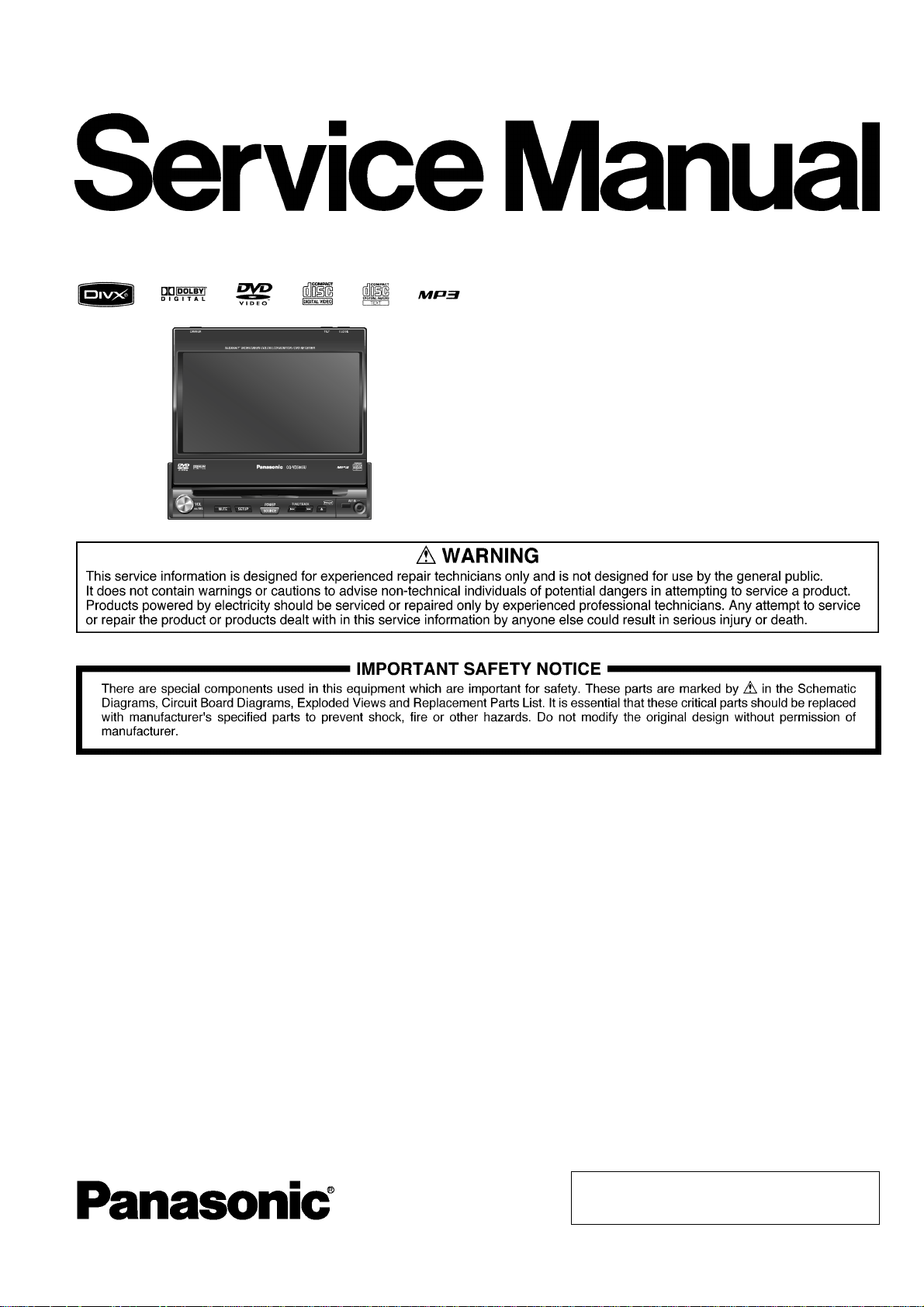
ORDER NO. ACED070201C7
C7
AUTOMOTIVE AFTERMARKET
CQ-VD5005U
CQ-VD5005L
In-Dash 7” Widescreen Color LCD Monitor/DVD Receiver
TABLE OF CONTENTS
PAGE P AGE
1 Service Navigation ----------------------------------------------- 2
2 Specifications ----------------------------------------------------- 3
3 Features ------------------------------------------------------------- 4
4 T ec hnic al Desc ri ptions----------------------------------------- 5
5 Disassembly and Assembly Instr uctio ns---------------10
6 Block Diagram----------------------------------------------------12
7 Wiring Connection Diagram---------------------------------15
8 Schematic Diagram---------------------------------------------16
9 Printed Circuit Board-------------------------------------------21
10 Exploded View and Replacement Parts List -----------28
11 Schematic Diagram for Printing with Letter Size-----44
© 2007 Matsushita Electric Industrial Co., Ltd. All
rights reserved. Unauthorized copying and distribution is a violation of law.
1 Service Navigation
1.1. About Lead Free Solder (PbF)
Distinction of PbF PCB :
• PCBs (manufactured) using lead free solder will have a Pb F
stamp on the PCB.
Caution :
• Pb free solder has a higher melting point than standard solder; Typically the melting point is 50 - 70°F (30 - 40°C)
higher. Please use a soldering iron with temperature control
and adjust it to 700 ± 20°F (370 ± 10°C). In case of using
high temperature soldering iron, please be careful not to
heat too long.
• Pb free solder will tend to splash when heated too high
(about 1100°F/600°C)
• This lead free solder will be used for the products after serial
No. 1,000,001.
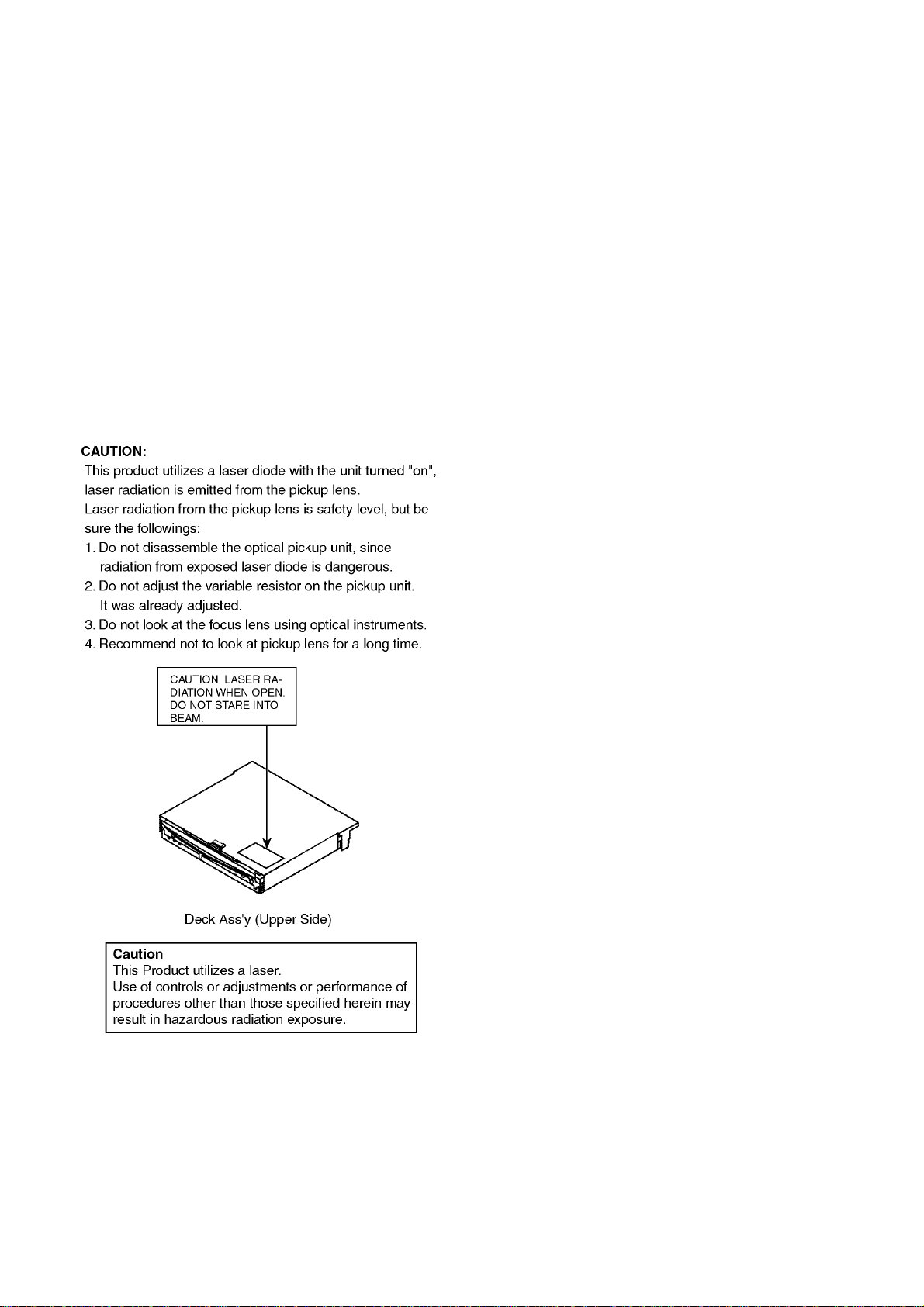
1.2. Laser Products
1.4. Maintenance
Your product is designed and manufactured to ensure a minimum of maintenance. Use a dry, a soft cloth for routine exterior
cleaning. Never use benzine, thinner or other solvents.
1.5. Notes
[RADIO BLOCK]
Do not align the AM/FM package block. When the package
block is necessary, it will be supplied alrea dy alig ned at the factory.
[DVD DECK BLOCK]
This model has no servo alignment points because microcomputer controls the servo circuit.
1.3. Replacing the Fuse
Use fuses of the same s pe cif ied rati ng 15 a mps. Using different
substitutes or fuses with higher ratings, or connecting the unit
directly without a fu se, could cause fire or damage to th e st ere o
unit.
2
2 Specifications
2.1. Specifications*
General
Power Supply DC 12V (11V - 16V)
Current Consumption Less than 10A (during disc playback)
Maximum Power Output 45 W x 4CH
Power Output 18 W x 4CH
Compatible Speaker Impedance
Video Input Signal Composite video signal, 1.0 Vp-p (75
Audio Input Sensitivity 2 Vrms
Video Output Signal Composite video signal, 1.0 Vp-p (75
Pre-Amp Output Voltage 2 Vrms
Pre-Amp Output Impedance Less than 600 Ω
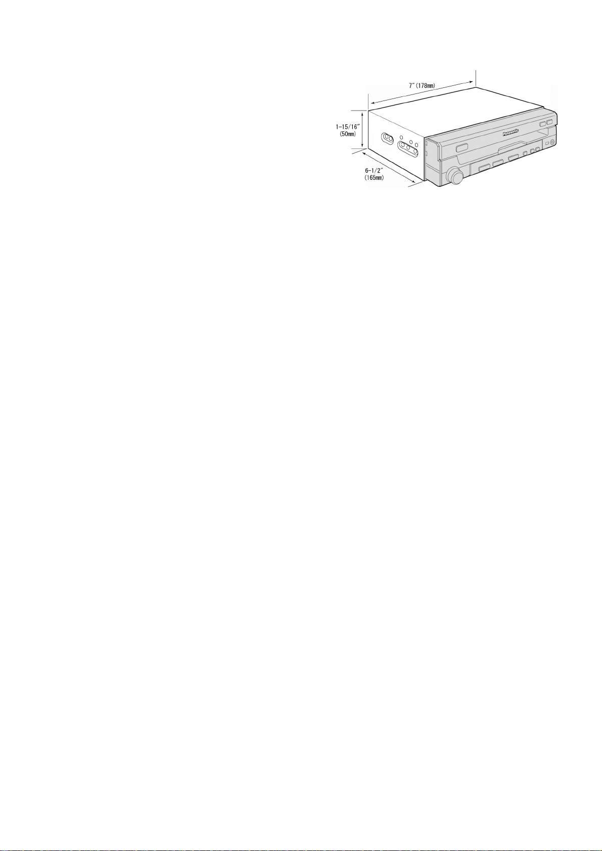
Dimensions (W×H×D)** 178×50×165mm (7”×1-15/16"×6-1/2")
Weight** 2.4 kg {5 lbs. 5 oz.}
Front AV input (AV1 IN)
Input Impedance 47 kΩ
Allowable External Input 2.0 V
Connector 3.5 mm stereo mini pin (Equipped with
Audio Input Sensitivity 2 Vrms
Video Output Signal Composite video signal, 1.0 Vp-p (75
Test Voltage 14.4V
Negative Ground
4 Ω
Ω)
Ω)
video input terminal)
Ω)
2.2. Dimensions
FM stereo radio
Frequency Range 87.9 MHz - 107.9 MHz
Usable Sensitivity 12.2 dBf
Stereo Separation 30 dB (at 1 kHz)
S/N ratio 62 dB
AM Radio
Frequency Range 530 kHz - 1710 kHz
Usable Sensitivity 28 dB/µV
Image Rejection Ratio 50 dB
Audio section
Output Voltage/Impedance 2 Vrms/600 Ω
Frequency Characteristics 20 Hz-20 kHz (±1 dB)
Dynamic Range 96 dB (during CD playback)
S/N ratio 95 dB (during CD playback)
Monitor
Liquid Crystal Panel 7” wide
Screen
Dimensions (W×H×D)**
Number of Pixels 336 960 pixels (234 vertical × 480 hor-
Valid Pixel Ratio Over 99.99%
Display Method Transparent color filter format
Drive Method TFT (Thin Film Transistor) active
154×87×177 mm (6-1/16”×3-7/16"×615/16")
izontal × 3)
matrix format
* Specifications and the design are subject to possible modification
without notice due to improvements.
** Dimensions and Weight shown are approximate.
*** Above specifications comply with EIA standards.
3

3 Features
• Integration of the monitor, FM/AM radio, DVD Video/Video
CD player and CD/MP3/DivX player.
• Built-in AV Input/Output Terminals.
• SQ3 (3-Band Sound Quality).
• GUI (Graphic User Interface).
• Disc type auto-detection.
• Touch Panel Operation.
• DVD-R, DVD-RW Playback.
•ID code.
• Differences Between 2 Models.
4
4 Technical Descriptions
4.1. Terminals Description
4.1.1. Main Block
IC601 :::: UPD70F32XXXB
Pin
No.
1 AVREF0 Reference voltage for A/D
2 AVSS Ground for A/D converter - 0 0 0
3 FREQ_CNT Output for control of fre-
4 TFT_RST RESET of TFT O 3.3 3.3 3.3
5 AVREF1 Reference voltage for A/D
6 MONI_CNT TFT monitor power supply
7 Touch_SW Switch output for touch
8 IC/FLMD0 Flash memory update con-
9 VDD +3.3V power supply - 3.3 3.3 3.3
10 REGC Bypass capacitor terminal
11 VSS Ground - 0 0 0
12 X1 Crystal osillator terminal for
13 X2 Crystal osillator terminal for
14 RESET System reset I 3.3 3.3 3.3
15 XT1 Crystal osillator terminal for
16 XT2 Not connected - - - 17 X+ Transistor SW output for
18 Y+ Transistor SW output for
19 X- Transistor SW output for
20 Y- Transistor SW output for
21 INV_PWR Inverter power supply con-
22 D_SDA I2C clock 2 O 3.3 3.3 3.3
23 D_SCL I2C data 2 O 3.3 3.3 3.3
24 N.C. - - 0 0 0
25 RDS_DATA Not connected - - - 26 RDS_CLK Not connected - - - 27 LED_ON LED control for SW sub-
28 REMO_DATAExternal remote control sig-
29 REMO_OUT Remote control code output O 3.3 3.3 3.3
30 REQUEST I2C communication request
31 NEJECT Output for compulsion eject O 3.3 3.3 3.3
32 LOADSW Loading SW I 0 0 0
33 EVSS Grand potential for external - 0 0 0
34 EVDD Positive power supply for
35 I2C_DATA I2C bus data output/ACK
36 I2C_CLK I2C bus clock output O 3.3 3.3 3.3
37 BEEP Beep correspondence title
38 CN_DET1 Input 1 for connector con-
Port Description I/O Vol (V)
FM AM DVD
-3.33.33.3
converter
O1.51.51.5
quency of DCDC
-3.33.33.3
converter
O2.52.52.5
control output
O2.82.82.8
panel SW detection
-000
trol
-2.52.52.5
for voltage reg.
I1.21.21.2
Main
-1.31.31.3
Main
I000
Sub
O3.33.33.3
touch panel X respect + pole
O3.33.33.3
touch panel Y respect + pole
O00 0
touch panel X respect-pole
O00 0
touch panel Y respect-pole
O3.33.33.3
trol output for monitor
O3.33.33.3
strate
I3.33.33.3
nal input
O0.10.10.1
(DVD module)
-3.33.33.3
external
O3.33.33.3
detection
O00 0
output
I000
nection confirmation
Pin
No.
39 PLL_CE Chip enable output for
40 PLL_SI Cereal data input for PLL_IC
41 PLL_SO Cereal data output for
42 PLL_CLK Cereal clock output for
43 E_SDA I2C clock 2 O 3.3 3.3 3.3
44 E_SCLK I2C data 2 O 3.3 3.3 3.3
45 MVR_DC PWM output for mechanism
46 PULSE Monitor start-up position
47 DECK_RST Reset output of DVD module O 3.3 3.3 3.3
48 FRG_IN Input for frequency count of
49 SRC_LED SRC button LED O 3.3 3.3 3.3
50 SRC_KEY SOURCE key detection I 3.3 3.3 3.3
51 SD Input for electric field
52 SYS_MUTE System mute signal output O 0 0 0
53 PR4_SI Disc Chucking SW I 3.3 3.3 3.3
54 PR4_SO Inner Limit SW I 0 0 0.35
55 PR4_SCK 8cm Eject SW Output or
56 BATT_SENSEBattery level detection I 3.3 3.3 3.3
57 ACC_SENSEACC level detection I 5.4 5.4 5.4
58 PANEL_DET Input for Detatchapanel
59 SYS_PWR System power control O 3.3 3.3 3.3
60 VideoSW1 SW1 for VideoSW switch O 3.3 3.3 3.3
61 VideoSW2 SW2 for VideoSW switch O 3.3 3.3 0
62 FAN_CNT FAN motor power supply
63 REVERSE Reverse detection I 3.3 3.3 3.3
64 EJECT_LED EJECT button LED O 0 0 0
65 SIDE_BRAKEParking brake detection I 0 0 0
66 NC Insertion entrance LED con-
67 AMP_CNT Amplifier control output O 3.3 3.3 3.3
68 ANT_CNT Antenna control output O 3.3 3.3 0
69 BVSS Ground for bus I/F - 0 0 0
70 BVDD Power supply for bus I/F - 3.3 3.3 3.3
71 PUSH_SW Signal input for rotary SW I 3.3 3.3 3.3
72 ROTARY.1 Rotary encoder signal (VOL
73 ROTARY.2 Rotary encoder signal (VOL
74 INIT_DET_2 Destination detection 2 I 0 0 0
75 INIT_DET_1 Destination detection 1 I 0 0 0
76 FLMD1 - - 0 0 0
77 REMO_CUT External remote control out-
78 HSD P.IC abnormality detection
79 AMP_STB Built-in power amplifier con-
80 AMP_MUTE Built-in p ower amplifier mu te
81 FRAM_HOLDNot connected - - - -
82 FRAM_CLK Not connected - - - 83 FRAM_DO Not connected - - - 84 FRAM_CS Not connected - - - -
Port Description I/O Vol (V)
FM AM DVD
O00 0
PLL_IC communication
I3.33.33.3
communication
O00 0
PLL_IC communication
O3.33.33.3
PLL_IC communication
O3.73.73.7
control
I5.15.15.1
detection pulse signal input
I1.51.51.5
DCDC
I5.25.24.5
strength detection
I/0 3.3 3.3 3.3
Forced Eject Input
I000
detection
O3.33.33.3
control
O00 0
trol when 2Din opens
I3.33.33.3
UP)
I3.33.33.3
DOWN)
O00 0
put stop signal output
I3.33.33.3
check
O00 0
trol output
O00 0
output
5

Pin
No.
85 FRAM_WP Not connected - - - 86 FRAM_DI F_RAM cereal data input O 3.3 3.3 3.3
87 Tilt_LED Tilt button LED O 3.3 3.3 3.3
88 MA Mechanism control terminalMAO3.33.33.3
89 MB Mechanism control terminalMBO3.33.33.3
90 MC Mechanism control terminalMCO3.33.33.3
Port Description I/O Vol (V)
FM AM DVD
91 CN_DET2 Input 2 for connector con-
nection confirmation
92 POSI_SENSEMonitor position voltage sig-
nal input
93 VSM Tuner S meter input I 2.2 1.3 1.1
94 AD_KEY1 AD_KEY input 1 I 3.3 3.3 3.3
95 AD_KEY2 AD_KEY input 2 I 3.3 3.3 3.3
96 AD_KEY3 AD_KEY input 3 I 3.3 3.3 3.3
97 XG Touch panel X respect-pole I 0 0 0
98 YG Touch panel Y respect-pole I 0.7 0.7 0.7
99 XR Touch panel X respect +
pole
100 YR Touch panel Y respect +
pole
I000
I2.42.42.4
I000
I0.70.70.7
6
4.2. IC Block Diagram
4.2.1. Main Block
IC51 : C1BB00001045
IC382 : C1AB00000084
IC604 : C0JBAC000390
IC201 : C1EA00000041
IC202 : C1BB00001132
IC701 : C0DAZHF00004
IC381 : C1AB00000163
IC702 : C0DBAZC00010
7
IC703 : C0CBABC00160
4.2.2. TFT Block
IC451 : C0DBAZA00017
IC704 : C0EBZ0000035
IC706 : C0DBCFG00003
IC452 : C0FBBD000065
IC710 : C0JBAZ000525
8
4.2.3. DVD Servo Block
IC104 : YESAM370
IC105 : YESAM294
IC107 : YESAM364
IC301 : YESAM405
9
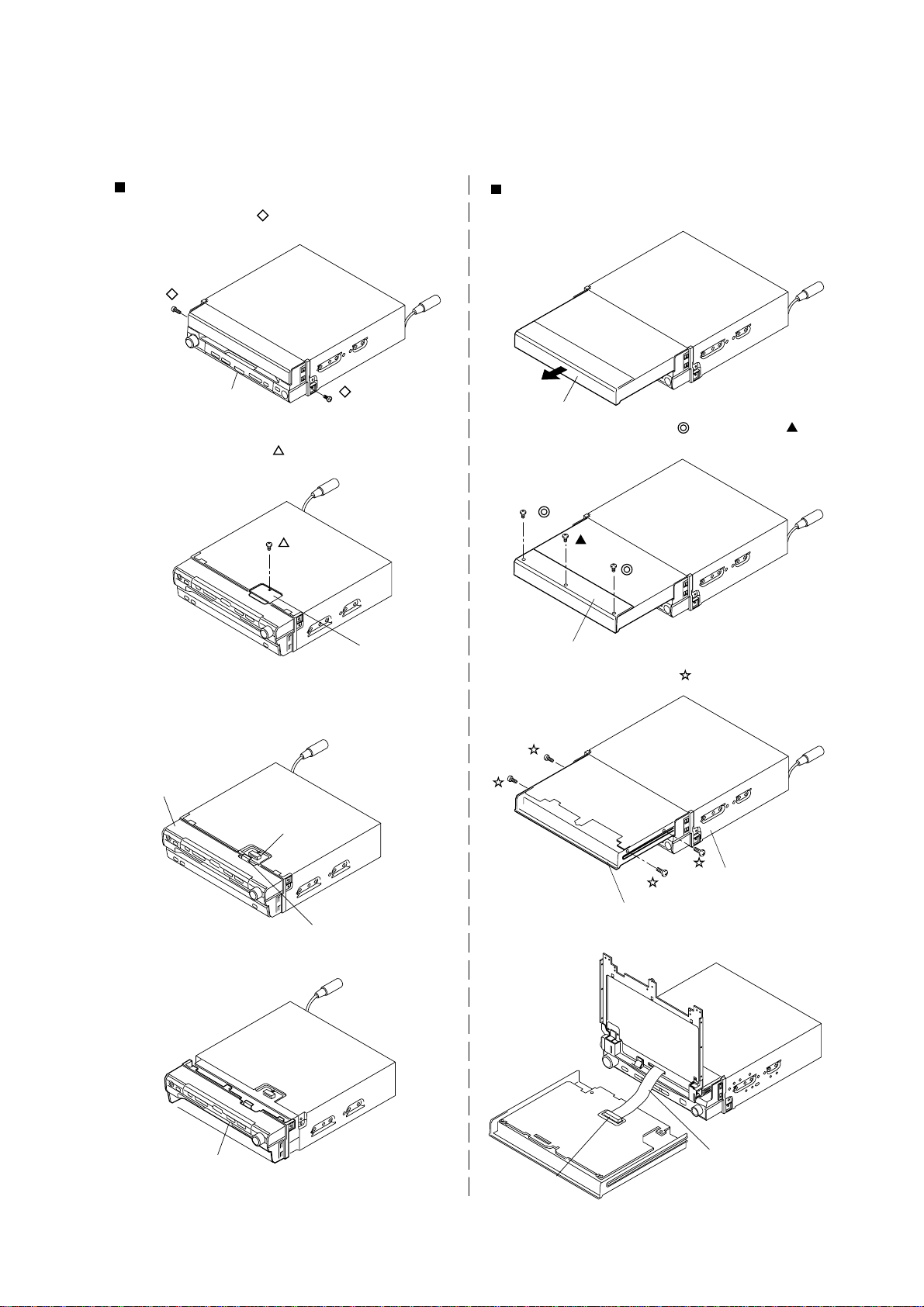
5 Disassembly and Assembly Instructions
5.1. How to Remove the Flexible PCB
Disassembly of Display Unit
Front Panel
. Remove the two screws( ) from the Front Panel.
Monitor
1. Pull out the Monitor to the arrow direction.
Front Panel
2. After removing the screw ( ) from the bottom side, remove
the Connector Cover.
Connector
Cover
3. Disconnect the FFC (CNP3), which is connected to
the Front Panel, from CN707 on the Main PCB (E-3173Aa).
Front Panel
CN707
Monitor
2. After removing the two screws ( ) and one screw ( ),
remove the Plate.
Plate
3. After removing the four screws ( ), remove the Monitor Ass'y.
4.Remove the Front Panel.
Front Panel
FFC (CNP3)
(Monitor Ass'y)
4. Disconnect the FPC Ass'y from CN452 on the TFT
PCB (E-9939A)
CN452
.
FPC Ass'y
10
Slide Mechanism
Ass'y
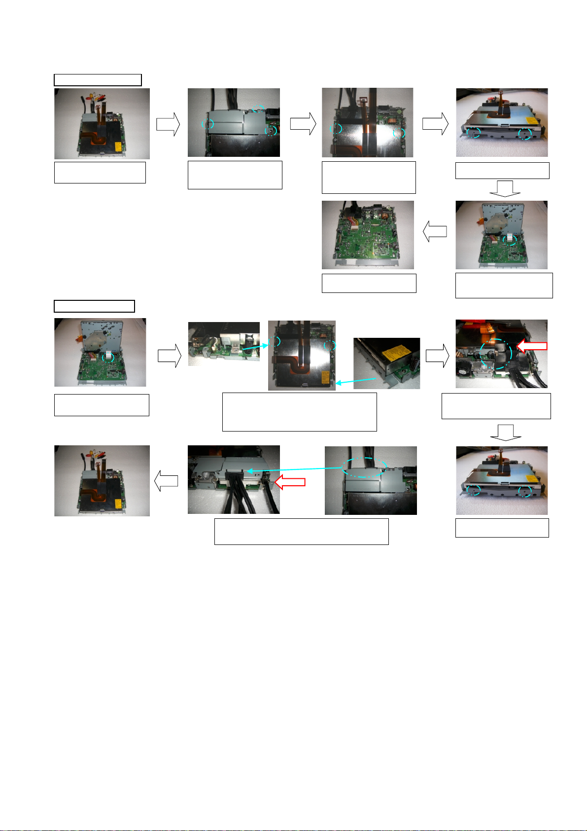
5.2. How to Disassemble & assemble
How to disassemble
First take off the monitor block
and must be as shown above.
How to assemble
Insert the flat cable.
(Caution for inserting diagonally)
Remove the screws from the 3
spots as shown above labled with
circles.
Match the mounting spots of the deck ass’y and fasten
them with 2 screws.
The deck ass’y must be inside the front plate of the under
cover.
Take off the metal that fixes the
connecter and remove the screws
from the 2 spots labled with circles.
Remove the deck block and it is
done.
Remove the screws from the
2spots labled with circles.
Must be situated as shown above
then remove the locks on the flat
cable of the deck.
Importan
With pad on the rear side of the deck
ass’y, there must me no gap between
the deck ass’y and the tuner shield case.
Importan
Match the connector bracket with the slit of the RCA cord ass’y
and fasten them with 3 screws.
Do not let the ANT receptacle wires get jammed.
Fasten the 2 parts labeled with a
circle with screws.
11
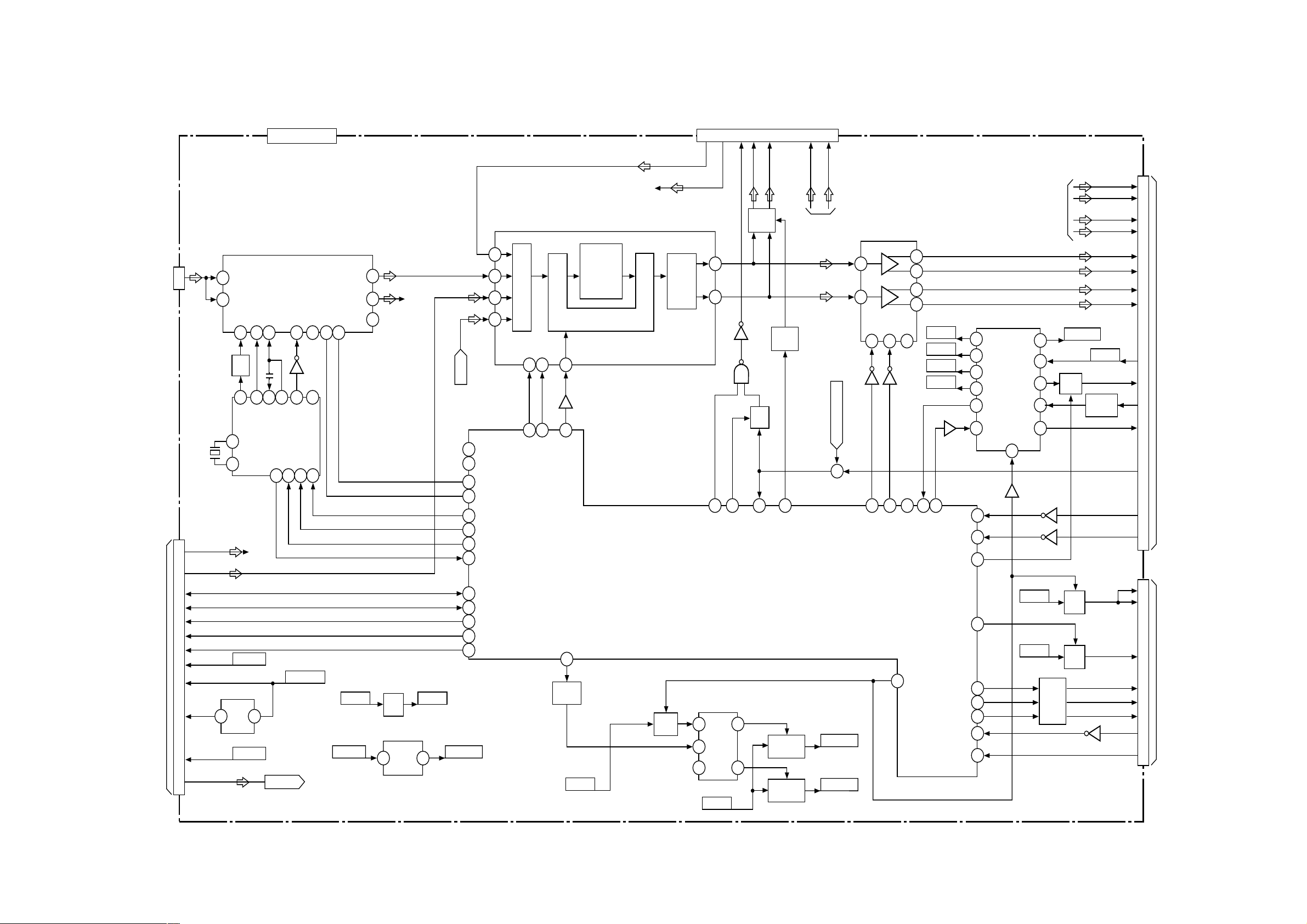
6 Block Diagram
6.1. Main-1 Block
ANT51
DVD
DECK
CN252
AUDIO R
23
AUDIO L
25
DATA
10
DCLK
11
REQUEST
12
NRESET
13
NEJECT
4
5,14,15
16–18
2.5V
19–22
6–9
VD OUT
28
E-3173A(1/2)
PA51
FM/AM TUNER
22 FM L-CH
1
AM
VT
OSC
IFC/ST REQ
FM
69
15 8 18 17 16
Q56
141720
FM
IFC
DVD VD
Q52
126
FM
ST REQ
DODICLK
SYS3.3V
LPF
X602
7.2MHz
1
24
IC51
PLL
IC706
2.5V
31
REG
PD
X OUT
X IN
R-CH
SYS5V
DVD8V
SD
FM ST/MONO
9
CONT
MONO
CE
2435
VDD5V
12
13
R-CH
FM
19
S METER
DET
AU9V
TU L
R-CH
DVD L
Q51
REG
TU+B
IC703
64
REG
VDD3.3V
7
9
SEL
11
5
AVI L
26 RDS CLK
25 RDS DATA
93 VSM
51 SD
39 PLL CE
42
PLL CLK
41 PLL SO
40 PLL SI
22 DSDA
23 DSCL
30 REQUEST
47 DRESET
31 NEJECT
CAR RADIO PROCESSOR
IC202
LOUDNESS,
VOLUME,
TONE
(T,M,B)
LINE SEL
SDA
SCL
23
22 3
Q303
43 44 37
E SCLK
BEEP
FRQ CNT
E SDA
3
Q713
FREQ
SHIFT
BATT
R-CH
Q719,720
PWR
AV2-L
FADER
SW
9 11 1 13 17 15 19
PRE FL
AV2-R
REMOTE
PRE RL
Q301
302
MUTE
FL
20
RL
19
Q211
Q604
212
MUTE
CONT
4
IC604
21
6
IC603
BUF
2
29
77
28
52
REM
REM CUT
SYS MUTE
REMO DATA2
IC601(1/2)
SYSTEM CONTROL
IC702
DC/DC CONV
9 VCC
2RT
15 SVP
7
10
Q706–708
ON/OFF
DRIVE
Q710–712
ON/OFF
BATT
DRIVE
PRE FR
PRE RR
R-CH
SYS3.3V
SYS5V
CN160
(1/2)
REMO DATA
+
IC201
POWER AMP
12
14
STBY
MUTE
42225
Q213
Q214
79
80
AMP STB
AMP MUTE
59
5
3
21
23
HSD
SW5V
DVD8V
VDD5V
AU9V
Q721,724
78
57
68
ANT CNT
AMP
ACC SENS
OFFSET DET
CNT
MVR DC
SYS PWR
PULSE
POSI SENSOR
REGULATORS
5
12
4
10
6
7
Q722
65
63
67
45
MA
88
89
MB
MC
90
46
92
IC701
ACC
SENS
ANT
CTRL
723
VCC
EXT
ACC
CTRL
11
AU9V
R-CH
14
8
Q701,702
1
3
2
Q703
Q705
BATT
Q612–614
INV
ILL10V
BATT
AMP CNT
PWR
SW
ACC
CHECK
ANT CNT
REMOTE
SIDE BRAKE
REVERSE
Q725,726
SW+B
PWR
SW
Q615–617
MVR DC
DC
ADJ
IC710
53
POSI SENSOR
CN701
FR+
FR-
RR+
RR-
FL+
FL-
RL+
RL-
ACC
MA
MB
MC
PULSE
CN708
(2/2)
1
3
5
7
2
4
9
11
15
6
13
8
14
10
12
37
38
32
35
34
33
36
31
POWER
PANEL
MOTOR
DRIVE
12
CQ-VD5005U/L MAIN(1/2)
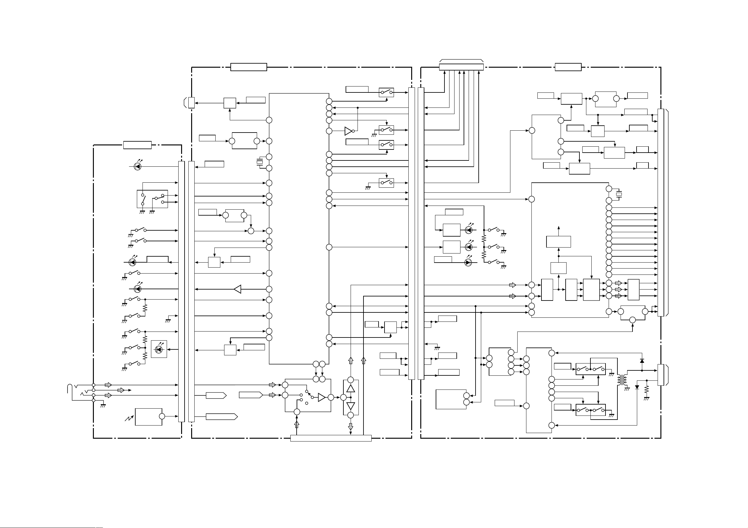
6.2. Main-2/TFT/SW Block
TOUCH PANEL
JK551
V
R
L
SW559
RESET
SW551
PANEL
SW555
SRC
SW558
EJECT
SW557
FF
SW553
MUTE
SW554
SET-UP
SW556
REW
E-9940A
SW552
R-CH
SW VDD
IC551
LIGHT
RECEIVE
CN256
15 15
3
2
1
16
16
10
10
13
13
12
12
11
7
5
4
20
20
17
17
8
1
3
2
1
11
7
5
4
8
FAN
CN551 CN707
1
FAN VCC
BATT
ILL10V
ENC PUSH
VDD5V
NRESET
PWR
SW
SW ILL 10V
AVI INV
AVI L
REM DATA
E-3173A(2/2)
Q155,156
PWR
SW
IC704
2
SYS5V
IC704
BATT
45
CHECK
X601
4.1943MHz
V
1
DET
+
Q151,152
VDD5V
Q610,727
PWR
SW
Q611,728
ILL 10V
DXD DV
SYSTEM CONTROL
62 FAN CNT
TOUCH PANEL
56 BATT SENS
12 X1
13 X2
71 PUSH SW
73 VOL UP
72 VOL DOWN
14 NRESET
58 PANEL DET
49 SRC LED
50 SRC KEY
64 EJECT LED
96 AD KEY3
38 CN DET1
95 AD KEY2
27 LED ON
1
3
A2 IN V
CN708
Y+
YR
YG
X+
XR
XG
X-
TILT LED
PWR
SW
CN DET2
(1/2)
Y-
29
26
25
30
27
24
23
28
13
20
15
14 14
17 17
19
21
22
8
9
7
10
11
12
Q603
(1/2)
Q602(2/2)
Q603(2/2)
BATT
CAMERA V
CN160(2/2)
Q602(1/2)
Q154,157
SYS5V
SYS3.3V SYS3.3V
IC601
18
Y+
100
YR
98
YG
20
Y-
7
17
X+
99
XR
97
XG
19
X-
MONI CNT
RSTB64
I2C CLK
VSW1
60 61
24
AB
IC382
94
87
35
36
21
91
VSW2
AD KEY1
TILT LED
I2C DATA
INV PWR
CN DET2
5
VIDEO SW
357
VIDEO
7
IC381
AMP
1
VIDEO
VDD3.3V
Q601
VDD3.3V
9
5
OUT V
CN452
29
26
25
30
27
24
23
28
MONI CONT
13
20
15
Q501
AV VIDEO
CAMERA
19
21
22
8
9
7
10
11
12
12653487
Y-
Y+
YR
YG
TFT3V
Q502
LED
DRIVE
LED
DRIVE
SYS5V
INV+B
SYS5V
IC802
EEPROM
X+
XR
XG
5
6
CN902
X-
SW501
OPEN/CLOSE
IC452
D/A CONV.
6
SDA
7
SCL
TFT5V
40
28
SW503
DIMMER
SW502
TILT
12
21
29
30
DC/AC INVERTER
1
3
2
14
3
17
4
5
E-9939A
SYS5V
IC401
DC/DC CONV.
EXT2
4
STBY
EXT3
47
VSW
8
SYS5V
IC801
VIDEO PROCESS
RSTB
LCD CONTROL
SIGNALS
TIMING
CONTROL
SYNC
SEP
SEL
SDA
SCL
IC451
2
OVP
ENA
DIM
RT
PDRA
NDRB
NDRD
PDRC
VDDA
FB
INV+B
19
20
11
12
INV+B
9
Q404
ON/OFF
DRIVE
SYS5V
ON/OFF
DRIVE
DEM
IC402
2.5V
15
REG
Q401,402
PWR
SW
SYS5V
Q403
MATRIX
Q451
Q452
CQ-VD5005U/L MAIN(2/2) / TFT/ SW
ON/OFF
DRIVE
82
XTALI
83
XTALO
49
STH1
50
STH2
44
OEH
52
CPH1
53
CPH2
54
CPH3
40
STV1
41
STV2
42
GOE
43
GCK
38
LR
39
UD
68
65
62
45 6 1
VCOM
FLICKER
TFT2.5V
TFT3.3V
Q405
X801
27MHz
Q805–810
AMP
IC901
VCOM
DRIVE
T451
TFT5V
-10V
+15V
3
CN901
STHR
STHL
STVD
STVU
OEV
CKV
LRC
UDC
VR
VG
VB
CN451
HV
3
23
16
5
1
TFT
17
PANEL
29
24
21
20
19
7
13
10
9
18
8
27
28
25
14
30
1
LV
LCD
2
BACKLIGHT
13
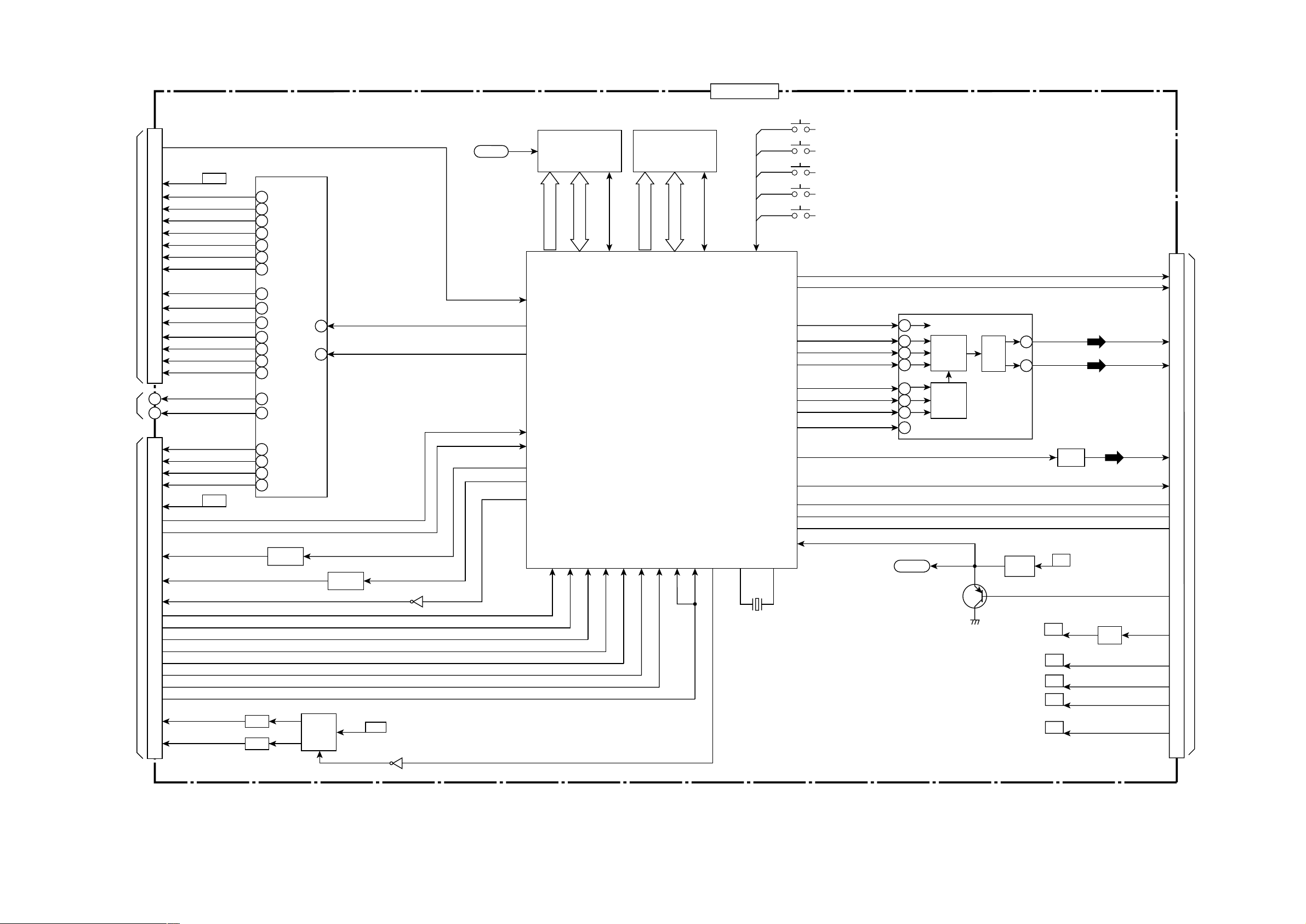
6.3. DVD Servo Block
3036-14-01
SPINDLE
MOTOR
Ass'y
LD
MOTOR
OPTICAL
PICK-UP
Ass'y
1
4
3
5
6
7
8
9
10
11
12
13
14
15
16
17
18
19
20
30
29
28
27
23
22
21
18
16
14
12
10
9
8
7
6
5
4
2
1
CN202
INNERSW
VH +
VH -
HW +
HW HV +
HV HU +
HU -
COILW
COILV
COILU
SL2 +
SL2 SL1 +
SL1 -
LD +
LD -
CN201
FO+
TR+
TRFO-
VCC5
T2
T1
CD LD+
DVD LD+
HFM
RF
TB
TA
TC
TD
F1
F2
IMON
CD VR
DVD VR
P5V
S5V
IC301
COIL/MOTOR DRIVE
7
HB
5
HW +
6
HW 3 HV +
4
HV 1
HU +
2
HU -
18
W
11
V
9
U
35
SL02 +
34
SL02 -
37
SL01 +
36
SL01 -
50 LDO +
49
LDO -
46
FCO +
TKO +
48
TKO -
47
FCO -
45
Q202,205
PWR
SW
Q212
SW
Q211
SW
LDIN
CTL2
Q203
26
23
PWR
SELECT
LD IN
Q201,206
PWR
SW
S5V
Q204
Q102
RESET
INNERSW
TRYDRV
DRIVEMUTE1
VIN 10
VIN 9
LPCO2
LPCO1
HFM
IC102 IC103
FLASH
MEMORY
FDT0-FDT15
FADR0-FADR20
81
91
80
CE,WE,OE
MA0-MA11
SDRAM
DQ0-DQ15
NCSM,NRAS,NCAS,
NWE,DQM0
MCK,DQM1,BA0,BA1
IC101
RF AMP
VIN4
VIN7
DSP
VIN8
LPC1
LPC2
DVR4
129
130
126
124
86
114 137 138 135 136 133 134 123 125 87 162 163
VIN2
VIN1
RF INP
VIN3
SW3
SW1
SW4
SW2
SW6
66, 67, 73, 74, 75
X101
12EJECT
8EJECT
DOWN SW
LOAD SW
DISC SW
OSD OSD
15
NEJECT NEJECT
13
IC105
AUDIO D/A CONVERTER
166
168
169
167
78
77
251
156
173
183
181
72
84
DACCK
SRCK
ADOUT3
LRCK
4
RESETOUT
DAC4OUT
IECOUT
VDI00
VDI02
REQUEST
NRST
MCLK
BICK
SDTI
LRCK
DAC-CSN
DAC-SDCK
DAC-SD0
PON
1
2
3
4
6
7
8
5
RESET
CLK
AUDIO
Data
I/F
UP
I/F
Q101
DAC
IC106
RESET
AOUT L
11
AOUT R
10
IC107
VIDEO
AMP
S5V
1.2V
3.3V
S5V
P5V
P8V
IC104,Q207
1.2V
REG
CN101
L-ch
R-ch
V OUT
IEC958
I2C-SDA (DATA)
I2C-SCL (DCLK)
REQUEST
N RESET
U2.5V
S3.3V
S5V
P5V
P8V
40
37
16
18
To
13
MAIN
BLOCK
11
31
30
29
28
19
20
21
22
23
24
25
26
27
36
32
33
34
35
14
CQ-VD5005U/L DVD Servo Block
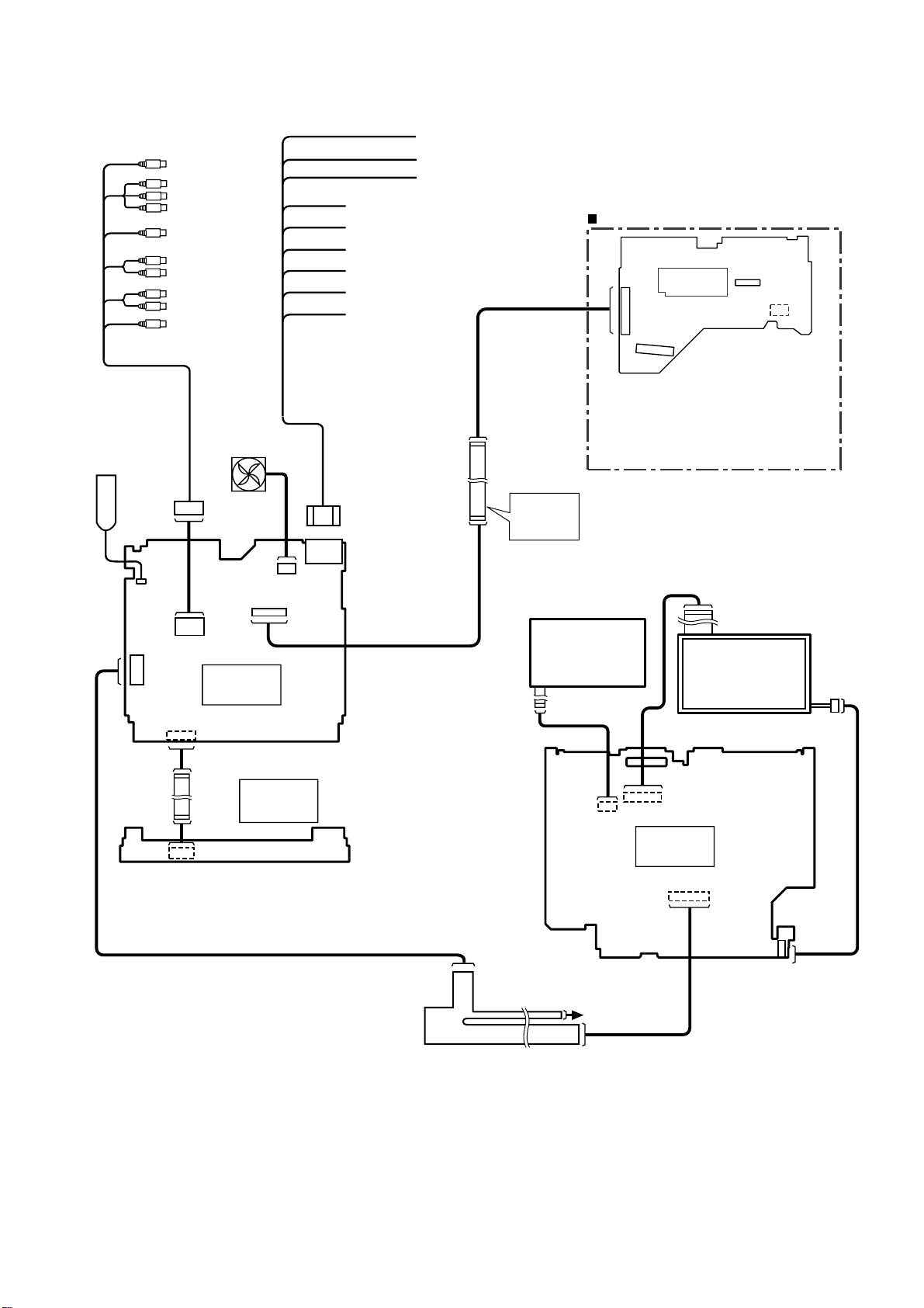
7 Wiring Connection Diagram
Battery
(Yellow)
(R)
(L)
(Yellow)
(Black)
(R)
(L)
(R)
(L)
(Yellow)
Camera Input
AV2-IN
Remote Out
Pre-Out Rear
Pre-Out Front
Video Out
External Amplifier Control Power
Side Brake (Parking Brake) Connection
Motor Antenna Relay Control
Reverse
4
/
4
/
Front SP
Rear SP
Ground
Power (ACC)
DVD Deck
CN101
CN201
DVD Servo P.C.B
[3036-14-01]
(Top Vie w)
40P
30P
CN202
20P
CN301
20P
Radio Antenna
Connector
ANT51
402
391
CN708
CN707
20 1
20 2
19 1
CN160
20
19
2
1
MAIN P.C.B
[E-3173Aa]
CNP3
CN551
FAN
3
CN256
CN252
140
SW P.C.B
[E-9940A]
1
CN701
Power
Connector
16 9
18
Extension
Connector
Jig Part No.
YESFZS2071
TOUCH PANEL
18
CN902
1
30
CN901
TFT P.C.B
[E-9939A]
LCD BACK LIGHT
CN452
1
30
FPC Ass'y
15
To Slide
Mechanism Ass'y
12
CN451
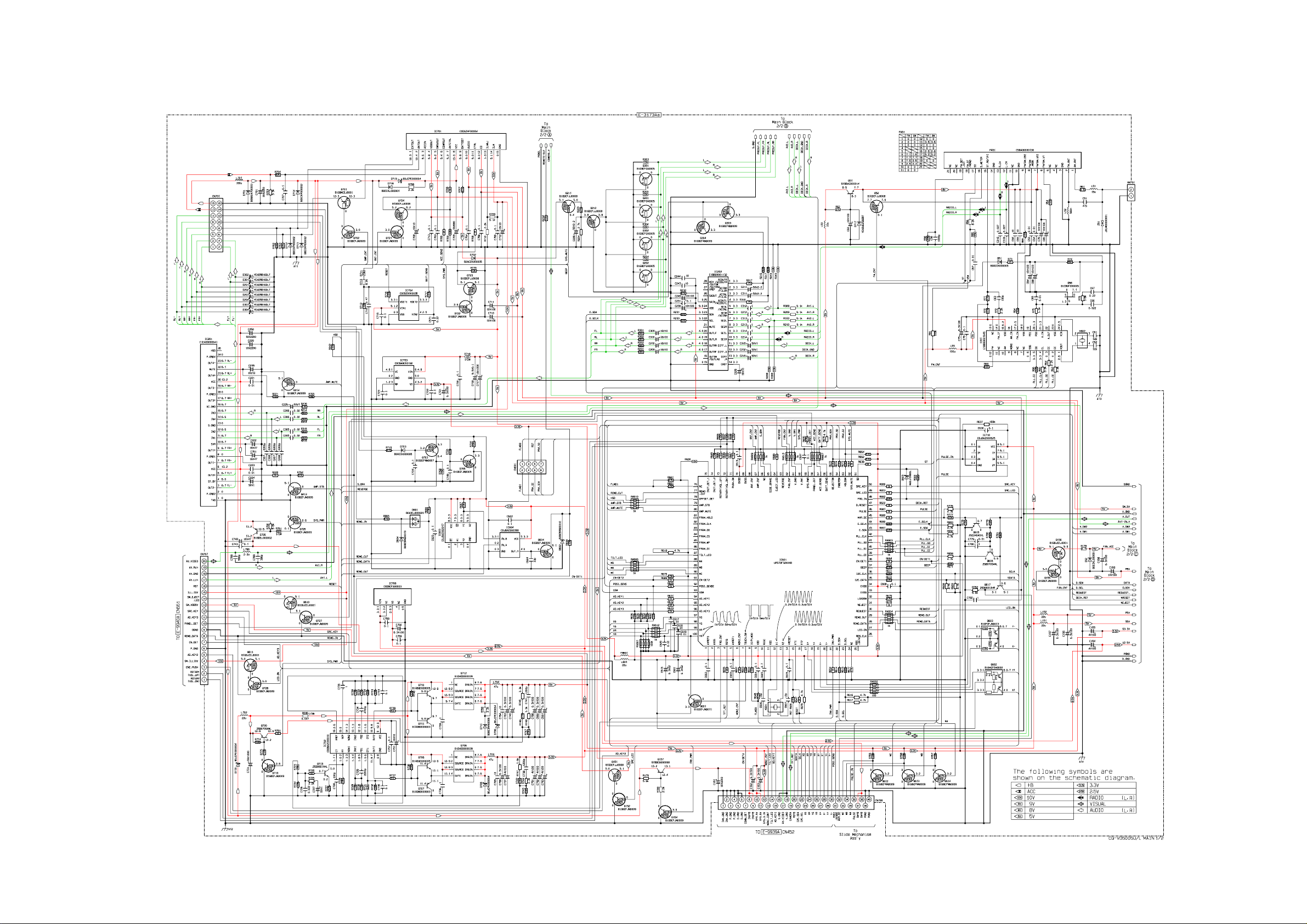
8 Schematic Diagram
8.1. Main-1 Block
16
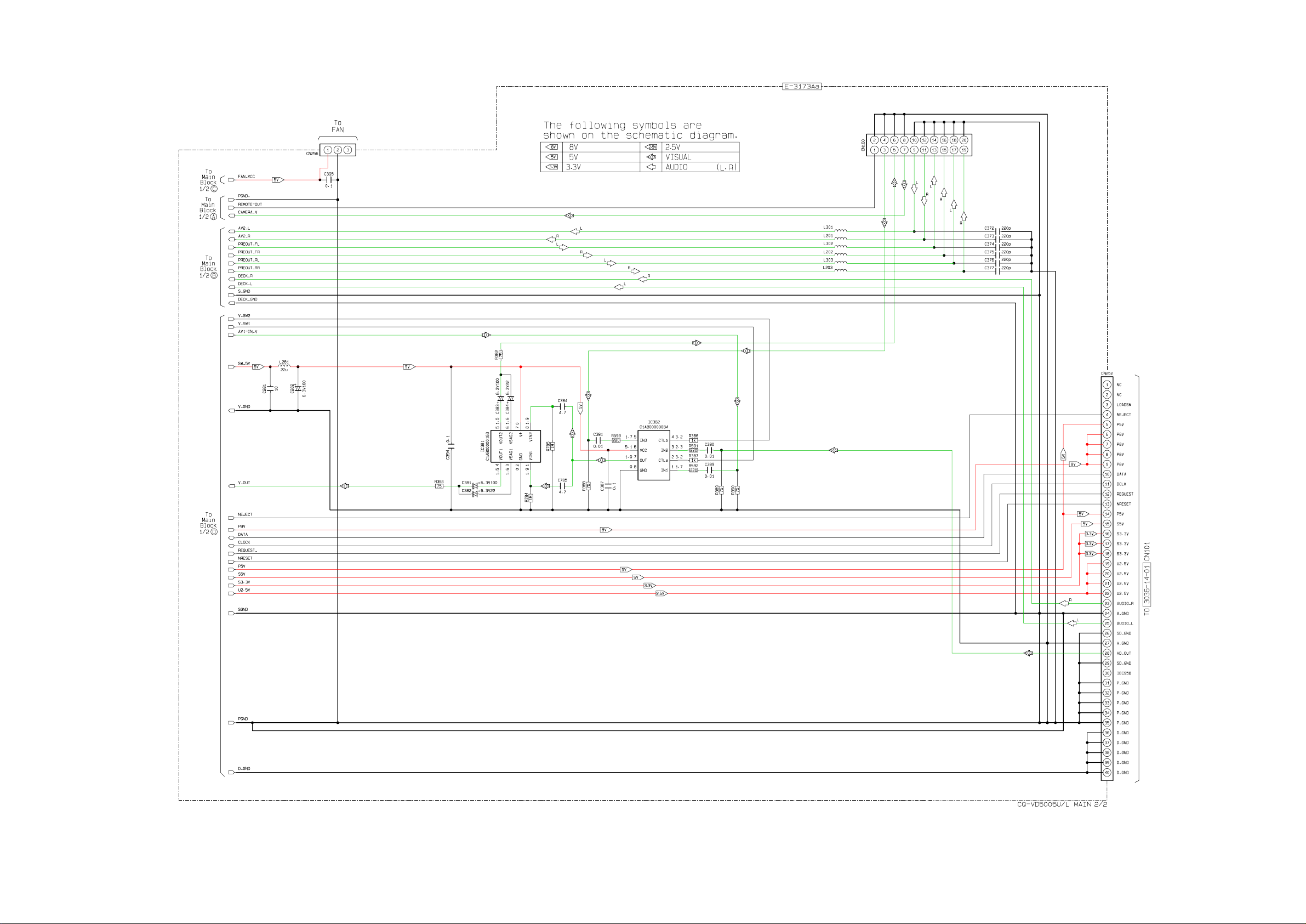
8.2. Main-2 Block
17
 Loading...