


CQ-C7301N
General
Power Supply DC 12V (11V - 16V),
Test Voltage 14.4V
Negative Ground
Tone Controls (Bass/Treble) Bass: ±12dB at 60Hz
Treble: ±12dB at 16kHz
Equalizer Center Frequency 60, 160, 400, 1k, 3k, 6k, 16k (Hz)
Variable Range of Equalizer -12dB to 12dB (2dB step)
Current Consumption Less than 2.2A
(CD mode; 0.5W × 4-speaker)
Maximum Power Output 50W × 4(at 4Ω)
Speaker Impedance 4-8Ω
Pre-amp Output Voltage
<CQ-C8351N,CQ-C8301N> 5V
<CQ-C7301N> 2.5V(CD mode)
Subwoofer Output Voltage
<CQ-C8351N,CQ-C8301N> 5V
<CQ-C7301N> 2.5V(CD mode)
Pre-amp Output Impedance
<CQ-C8351N,CQ-C8301N> 60Ω
<CQ-C7301N> 200Ω
Subwoofer Output Impedance
<CQ-C8351N,CQ-C8301N> 60Ω
<CQ-C7301N> 200Ω
CD Player
Sampling Frequency 8 Times Oversampling
Pick-up Type Astigma 3-Beam
© 2005 Matsushita Electric Industrial Co., Ltd. All
rights reserved. Unauthorized copying and
distribution is a violation of law.
CQ-C8351N
CQ-C8301N
CQ-C7301N
WMA MP3 CD Player/Receiver with Full
Dot Matrix Display
Light Source Semiconductor Laser
Wave Length 790 nm
Frequency Response 20 Hz-20kHz (±1dB)
Signal to Noise Ratio 96dB
Total Harmonic Distortion 0.01% (1kHz)
Wow and Flutter Below Measurable Limits
Channel Separation 75dB
FM Stereo Radio
Frequency Range 87.5MHz - 108MHz
Usable Sensitivity 6dB/µV (S/N 30dB)
Stereo Separation 35dB (at 1kHz)
AM Radio(MW)
Frequency Range 531kHz - 1,602kHz
Usable Sensitivity 28dB/µV (S/N 20dB)
AM Radio(LW)
Frequency Range 153kHz - 279kHz
Usable Sensitivity 32dB/µV (S/N 20dB)
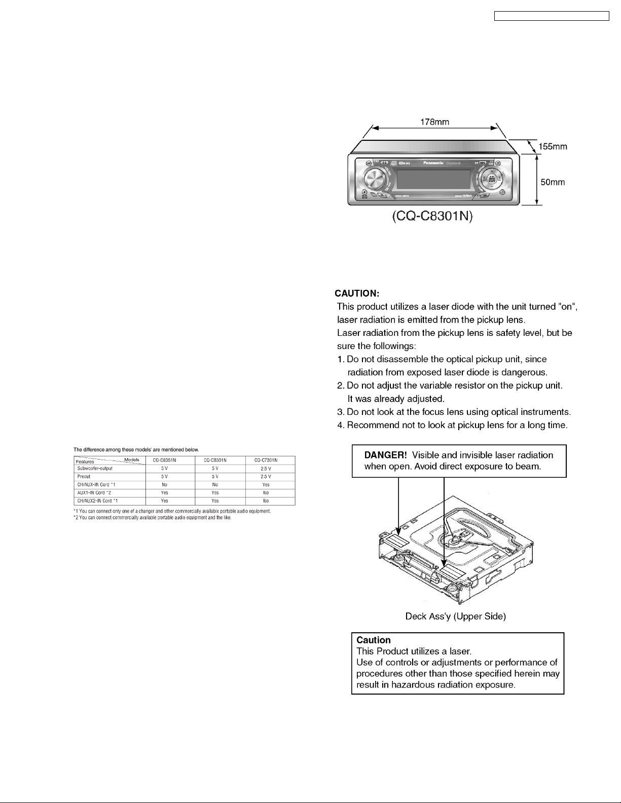
Dimensions (W×H×D)**
178×50×155mm
Weight** 1.6 kg
* Specifications and the design are subject to possible modification
without notice due to improvements.
** Dimensions and Weight shown are approximate.
** Above specifications comply with EIA standards.
AUTOMOTIVE AFTERMARKET
Specifications*
ORDER NO. ACED050211C8
1 ABOUT LEAD FREE SOLDER (PbF) 3
2 FEATURES
3
3 REPLACEING THE FUSE
3
4 MAINTENANCE
3
5 NOTES
3
6 DIMENSIONS
3
7 LASER PRODUCTS
3
8 WIRING CONNECTION
4
9 BLOCK DIAGRAM
6
10 DISASSEMB LY INSTRUCTI ONS
10
11 TERMINALS DESCRIPTION
13
12 IC BLOCK DIAGRAM
17
13 REPLACEM ENT PARTS LIST [CQ-C8351N/C8301N]
21
14 EXPLODED VIEW (Unit) [CQ-C8351N/C8301N]
27
15 REPLACEM ENT PARTS LIST [CQ-C7301N]
28
16 EXPLODED VIEW (Unit) [CQ-C7301N]
34
17 CD PLAYER PARTS LIST
35
18 EXPLODED VIEW (CD PLAYER)
38
19 WIRING DIAGRAM
39
20 SCHEMATIC DIAGRAM
45
CONTENTS
Page Page
2
CQ-C8351N / CQ-C8301N / CQ-C7301N
1 ABOUT LEAD FREE
SOLDER (PbF)
Distinction of PbF PCB:
PCBs (manufactured) using lead free solder will have a PbF
stamp on the PCB.
Caution :
•
• •
• Pb free solder has a higher melting point than standard
solder; Typically the melting point is 50 - 70°F (30 -
40°C) higher. Please use a soldering iron with
temperature control and adjust it to 700 ± 20°F (370 ±
10°C). In case of using high temperature soldering iron,
please be careful not to heat too long.
•
• •
• Pb free solder will tend to splash when heated too high
(about 1100°F/600°C)
•
• •
• This lead free solder will be used for the products after
serial No. 1,000,001.
2 FEATURES
•
• •
• MP3/WMA Playback from CD-R/RW
•
• •
• Fully Motorized Front Panel
•
• •
• Innovated APM (Auto Preset Memory) method
•
• •
• Six Preset Modes (FLAT, ROCK, POP, VOCAL, JAZZ,
CLUB)
•
• •
• SQ7 (7 Bands Sound Quality)
•
• •
• CD Changer Control
•
• •
• DVD Changer Control
•
• •
• Customize the Display (Customize Function)
•
• •
• Delightful sound space thanks to system buildup
•
• •
• The difference among these models’ are mentioned below.
3 REPLACEING THE FUSE
Use fuses of the same specified rating 15 amps. Using different
substitutes or fuses with higher ratings, or connecting the unit
directly without a fuse, could cause fire or damage to the stereo
unit.
4 MAINTENANCE
Your products is designed and manufactured to ensure a
minimum of maintenance. Use a soft cloth for routine exterior
cleaning. Never use benzine, thinner or other solvent.
5 NOTES
[RADIO BLOCK]
Do not align the AM/FM package block. When the package
block is necessary, it will be supplied already aligned at the
factory.
[CD DECK BLOCK]
This model has no servo alignment points because
microcomputer controls the servo circuit
6 DIMENSIONS
7 LASER PRODUCTS
3
CQ-C8351N / CQ-C8301N / CQ-C7301N
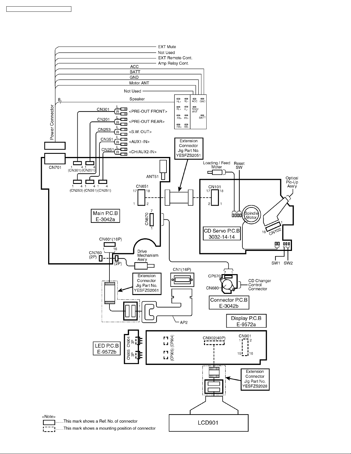
8 WIRING CONNECTION
8.1. CQ-C8351N/C8301N
4
CQ-C8351N / CQ-C8301N / CQ-C7301N
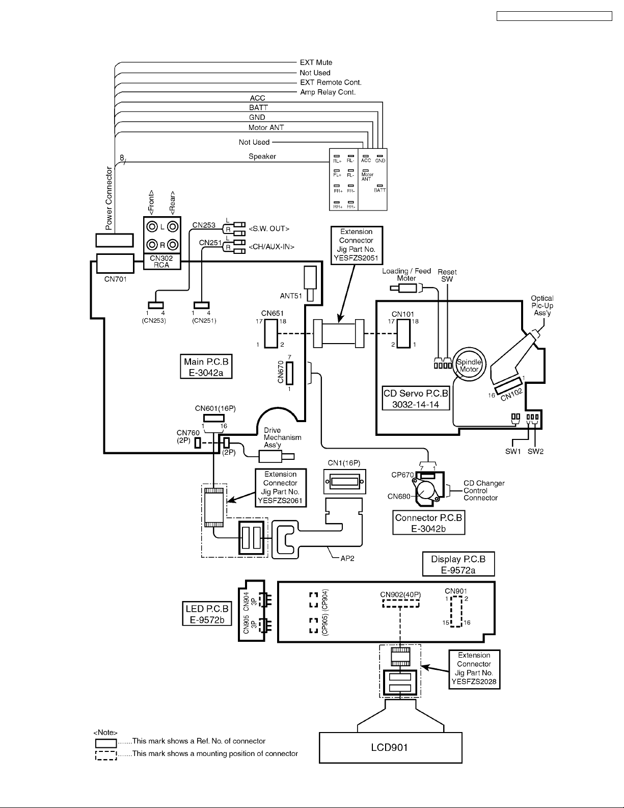
8.2. CQ-C7301N
5
CQ-C8351N / CQ-C8301N / CQ-C7301N
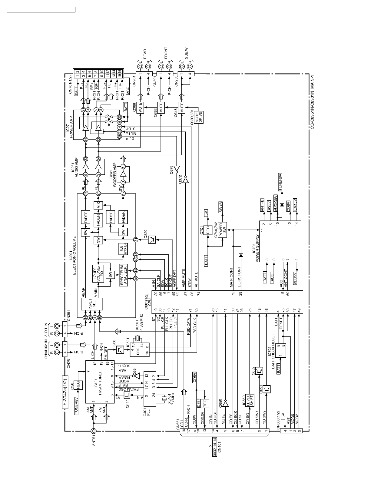
9 BLOCK DIAGRAM
9.1. Main-1 Block [CQ-C8351N/C8301N]
6
CQ-C8351N / CQ-C8301N / CQ-C7301N
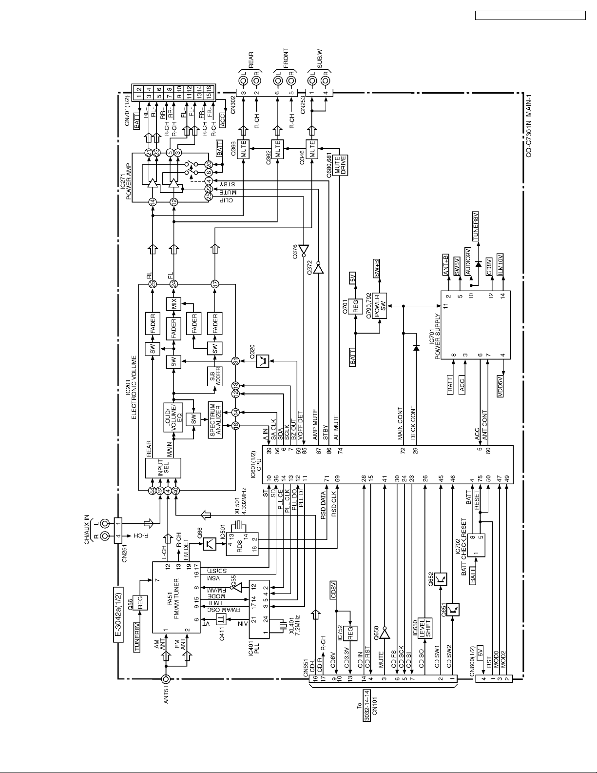
9.2. Main-1 Block [CQ-C7301N]
7
CQ-C8351N / CQ-C8301N / CQ-C7301N

9.3. Main-2/Display/LED Block
8
CQ-C8351N / CQ-C8301N / CQ-C7301N
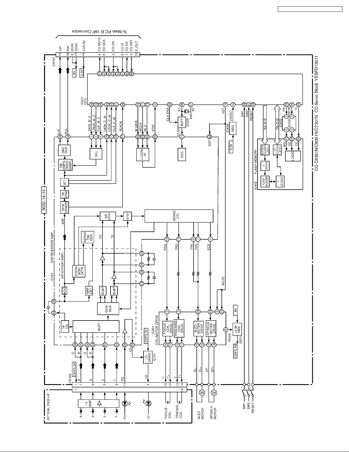
9.4. CD Servo Block
9
CQ-C8351N / CQ-C8301N / CQ-C7301N
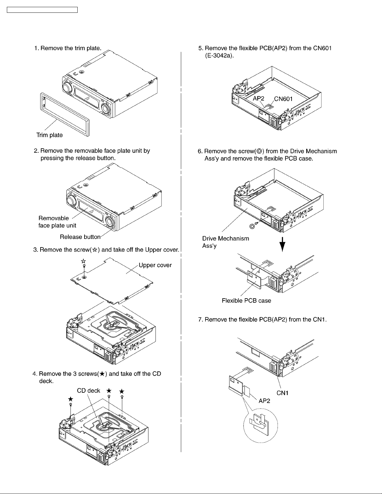
10 DISASSEMBLY INSTRUCTIONS
10.1. How to Remove the Flexible PCB(AP2)
10
CQ-C8351N / CQ-C8301N / CQ-C7301N
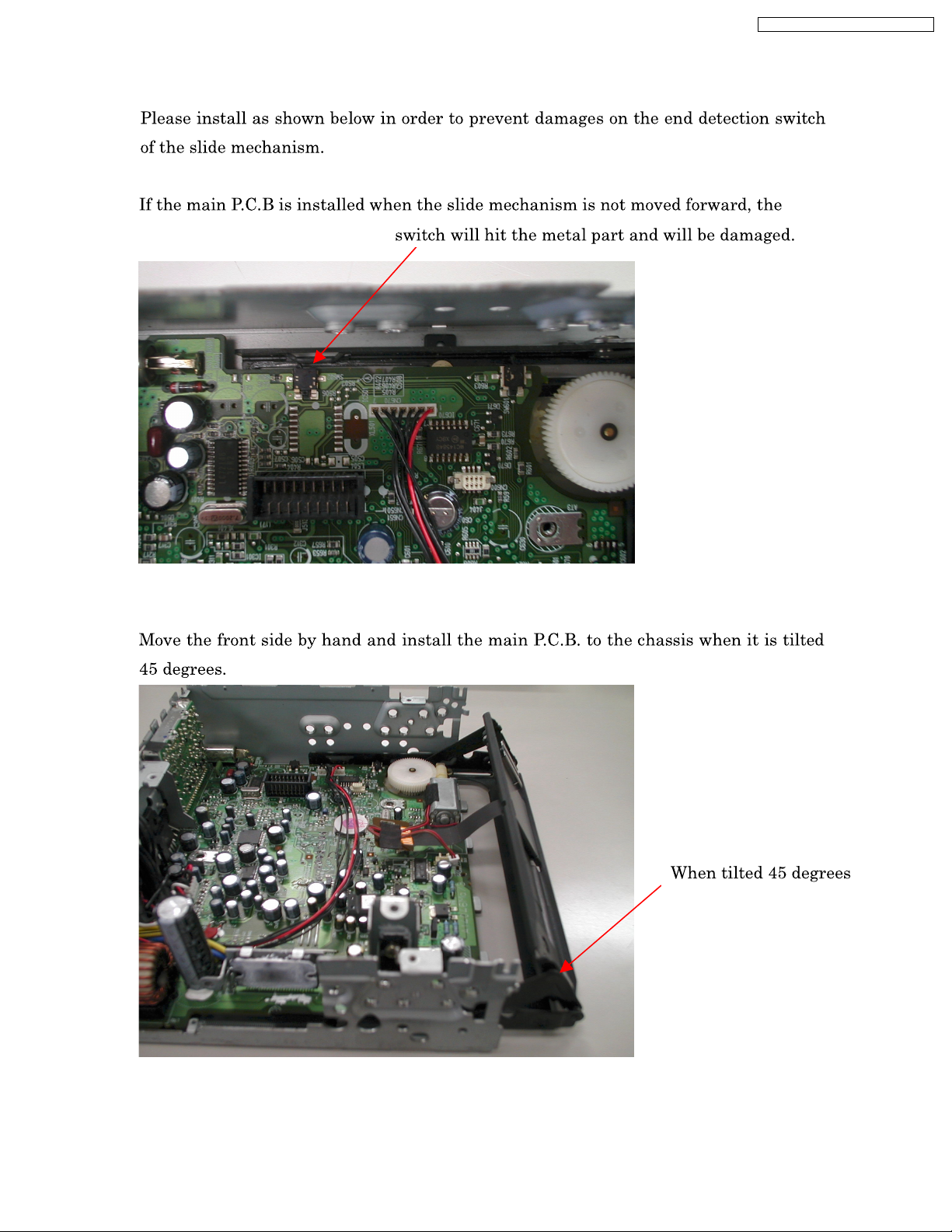
10.2. How to Install the Main P.C.B. of the Electric Display
11
CQ-C8351N / CQ-C8301N / CQ-C7301N

12
CQ-C8351N / CQ-C8301N / CQ-C7301N
11.1. Main Block
IC601 : C2CBKG000018
Pin
No.
Port Description (I/O) (V)
FM AM CD
1 PANEL OPEN PANEL OPEN detection I 0 5.2 5.2
2 PANEL
CLOSE
PANEL CLOSE detection I 0 0 5.2
3 NC No Connection - - - -
4 BATT BATT detection I 4.8 5 5
5 ACC ACC detection I 4.8 5 5
6 SDA Electronic VOL data I/O 4.9 4.9 4.9
7 SCK Electronic VOL clock O 4.9 4.9 4.9
8 NC No Connection - - - -
9 Vss Power supply GND I 0 0 0
10 ST FM ST detection I 5.1 5.2 5.2
11 PLL DI(MO) PLL data output O 0.6 0 0
12 PLL DO(MI) PLL data input I 5.2 5.2 5.2
13 PLL CLK PLL clock output O 4.9 4.9 4.9
14 PLL CE PLL chip enable output O 0 0 0
15 CD RST CD deck reset output O 4.9 4.9 4.9
16 SUB SI SUB u-com Data trans SO 0.6 0.6 0.8
17 NC No Connection - - - -
18 SUB SO SUB u-com data recept SI 4.4 4.4 4.4
19 CH DATA CD Data recept/FLASH
WSO
SI 1.6 1.6 1.6
20 CH CLK CD clock
transmit/FLASH W CLK
SCK 4.9 4.9 4.9
21 Vdd Power supply I 4.9 4.9 4.9
22 XM SI CD Data transmit/FLASH
WSI
S0 0 0 0
23 SD SI - - - - -
24 CD SCK Clock recept from
Changer
SCK 0 0.4 0
25 CONDENSOR Capacitor for power
supply
- 3.3 3.3 3.3
26 CD SO Data recept from
Changer
SI 0 0 0
27 CH STB Changer stororb signal
input
INT 0 0 0
28 CD IN DISC in detect I 4.9 4.9 0.4
29 DECK V
CONT
DECK power supply
control output
O 4.9 4.9 4.9
30 CD FS Strobe signal for CD
communication
O 3.7 3.7 3.7
31 NC No Connection - - - -
32 Avdd Power supply of D/A
converter
I 5.1 5.1 5.1
33 AVREF Reference voltage for
D/A converter
I 5.1 5.1 5.1
34 AVGND Reference GND for D/A
converter
I 0 0 0
35 AVSS Grand for A/D and D/A
converter
I 0 0 0
36 SD FM/AM signal meter
signal input
A/D 0.2 0 0.3
37 INIT A Initializ A (CQ-C7401U) A/D 0 0 0
38 INIT B Initializ B A/D 0 0 0
39 AIN SPE.ANA A.IN A/D 0 0 0
40 Vss GND I 0 0 0
41 CD MUTE CD deck mute detection I 0 0 5.1
42 NC No Connection - - - -
43 NC No Connection - - - -
44 NC No Connection - - - -
45 CD SW1 CD disc in detection I - - -
46 CD SW2 CD disc in detection I - - -
47 MOD0 Operating mode input 0 I 5.1 5.1 5.1
48 MOD1 Operating mode input 1 I 5.1 5.1 5.1
Pin
No.
Port Description (I/O) (V)
FM AM CD
49 MOD2 Operating mode input 2 I 0 0 0
50 H STANDBY External standby input I 5 5 5
51 NC No Connection - - - -
52 FP MOTOR1 Front open/close control
1
O 4.9 5 4.9
53 FP MOTOR2 Front open/close control
2
O 4.9 5 4.9
54 V CNT1 Panel driving voltage
control 1
O 0 0 5
55 V CNT2(NC) No Connection - - - -
56 SA CLK Control for Speana
acquisition
O 5 5 4.9
57 EXT MUTE TEL/NAVI MUTE input I 5.3 5.2 5.2
58 AMP CONT External AMP control O 4.9 5 4.9
59 BZ-OUT Buzzer output PPG 0 0 0
60 ANT CONT Motor antenna control O 4.9 5 0
61 DIM1 Dimmer control output 1 O 0 0 0
62 DIM2 Dimmer control output 2 O 0 0 0
63 CDC REM
OUT
Remote control code
output to Changer
O 5 5 5
64 CDC SENS CDC 1/2 detection I 5.1 5.1 5.1
65 CDC 1/2 CDC 1/2 change output O 0 0 0
66 NC No Connection - - - -
67 MWUP MAIN.WAKE.UP.REQ
input
I 5 4.9 5
68 NC No Connection - - - -
69 RDS CLK
70 NC No Connection - - - -
71 RDS DATA - - - -
72 MAIN CONT MAIN power supply
control output
O 4.9 4.9 4.9
73 INV CONT INV power supply control
output
O 5 5 5
74 AF MUTE Tr-MUTE control O/I 5 5 5
75 RESET Reset input I 5 5 5
76 NC No Connection - - - -
77 NC No Connection - - - -
78 NC GND I 0 0 0
79 Vss GND I 0 0 0
80 X1 Crystal oscillator input I 2 2 2
81 X2 Crystal oscillator output O 2.5 2.5 2.5
82 Vdd Power supply I 5 5 5
83 P00 Pldaun port for writing I 0 0 0
84 P01 Pull-up port for writing I 5.1 5 5.1
85 VOFF DET PWR-IC OFFSET
detection
I 0 0 0
86 STBY PWR-IC STBY control
output
O 5 5 5
87 AMP MUTE PWR-IC MUTE control
output
O 0 0 0
88 ILL SENS External dimmer control
input
I 5 5 5
89 SUBM CNT 3.3V control for SUB
microcomputer
O 5 5 5
90 NC No Connection - - - -
91 NC No Connection - - - -
92 NC No Connection - - - -
93 SWUP SUB.WAKE.UP.REQ O 4.9 5 4.9
94 DISPM CNT Power supply control
output of display 5V
O/I 0 0 0
95 EJE ILL(NC) No Connection - - - -
96 NC No Connection - - - -
97 NC No Connection - - - -
98 S LED Security LED control
output
O 0 0 5
99 PANEL IN PANEL detect I 5.2 5.2 5.2
11 TERMINALS DESCRIPTION
13
CQ-C8351N / CQ-C8301N / CQ-C7301N
Pin
No.
Port Description (I/O) (V)
FM AM CD
100 EP CS(NC) No Connection - - - -
11.2. Display Block
IC900 C2CBJH000105
Pin
No.
Port Part Name & Description I/O (V)
1 A18 FLASH A17 O 1.5
2 A19 FLASH A18 O 1.7
3 A20 FLASH A19 O 1.3
4 NC No Connection - -
5 LED.G - - -
6 LED.B - - -
7 A0 LCD driver data or command
distinction
O 1.3
8 A1 FLASH A0 O 0.3
9 VSS Ground potential - 0
10 A2 FLASH A1 O 0.4
11 A3 FLASH A2 O 0.4
12 A4 FLASH A3 O 0.4
13 A5 FLASH A4 O 1.3
14 A6 FLASH A5 O 0.4
15 A7 FLASH A6 O 0
16 A8 FLASH A7 O 1.3
17 A9 FLASH A8 O 0
18 A10 FLASH A9 O 0
19 A11 FLASH A10 O 1.5
20 A12 FLASH A11 O 1.7
21 VCC Positive power supply
terminal
- 3.5
22 A13 FLASH A12 O 1.4
23 A14 FLASH A13 O 1.6
24 A15 FLASH A14 O 1.7
25 SUB SI/UP SO MAIN-u-com communication
data input and external flash
rewritting
- 0.5
26 SUB SO/UP SI MAIN-u-com communication
data output and external
flash rewritting
O 1.8
27 UP CLK External flash rewritting
switch
I 3.5
28 NC No Connection - -
29 FLASH RESET FLASH reset control output O 3.5
30 KS1 Key scan signal 1 output I 0
31 NC No Connection - -
32 NC No Connection - -
33 AVCC Positive power supply for A/D
converter
- 3.5
34 AVRH A/D converter standard
voltage input
- 3.5
35 AVSS/AVRL A/D converter ground
potential
- 0
36 TH DETECT Temperature detection input I 1.3
37 KS2 Key scan signal 2 output I 0
38 KS3 Key scan signal 3 output I 0
39 NC No Connection - -
40 VSS Ground potential - 0
41 KI5 Key return signal 5 input I 0
42 KI4 Key return signal 4 input I 0
43 KI3 Key return signal 3 input I 0
44 KI2 Key return signal 2 input I 0
45 NC FLASH writing program
starter
I 0
46 NC FLASH writing program
starter
I 3.5
47 MD0 Mode setting terminal I 3.5
48 MD1 Mode setting terminal I 3.5
49 MD2 Mode setting terminal I 0
50 S W U REQ SUB-u-com wake up request INT 3.0
51 ROTARY.1 Rotary encoder signal 1(VOL
UP)
I 2.5
52 ROTARY.2 Rotary encoder signal 2 (VOL
DOWN)
I 2.5
14
CQ-C8351N / CQ-C8301N / CQ-C7301N
Pin
No.
Port Part Name & Description I/O (V)
53 KI1(SOURCE) Key return signal 1 INT/I 0
54 REMO INT Remote control signal
interference
INT 3.7
55 NC No Connection - -
56 NC No Connection - -
57 NC No Connection - -
58 FLASH CE FLASH chip enable O 3.4
59 LCD CS LCD driver chip select O 3.4
60 LER R - - -
61 NC No Connection - -
62 REMO 1 Remote control signal I 3.7
63 NC No Connection - -
64 VLCD CONT VLCD 16V control O 3.4
65 M W U REQ MAIN-u-com wake up request O 0
66 LED ON P.LED control output O 3.4
67 NC No Connection - -
68 NC No Connection - -
69 FLASH OE/ LCD
RD
FLASH output enable and
LCD driver lead strobe
O 3.4
70 LCD WR LCD driver light strobe signal O 3.4
71 FLASH WE FLASH light enable signal O 3.4
72 NC No Connection - -
73 LCD RESET LCD driver reset control O 3.4
74 FLASH RY/BY FLASH ready/busy input I 3.4
75 /RST System reset signal input I 3.5
76 NC No Connection - -
77 X1A(NC) No Connection - -
78 X0A Not used I 0
79 VSS Ground - 0
80 X0 MAIN system clock input
(12.5MHz)
I 1.3
81 X1 MAIN system clock output
(12.5MHz)
O 1.5
82 VCC Positive power supply - 3.5
83 D0 FLASH D0/LCD D0 I 0.9
84 D1 FLASH D1/LCD D1 I 0.9
85 D2 FLASH D2/LCD D2 I 1.1
86 D3 FLASH D3/LCD D3 I 0.9
87 D4 FLASH D4/LCD D4 I 1.0
88 D5 FLASH D5/LCD D5 I 1.1
89 D6 FLASH D6/LCD D6 I 1.1
90 D7 FLASH D7/LCD D7 I 0.8
91 D8 FLASH D8 I/O 0.9
92 D9 FLASH D9 I/O 0.9
93 D10 FLASH D10 I/O 0.9
94 D11 FLASH D11 I/O 0.8
95 D12 FLASH D12 I/O 0.8
96 D13 FLASH D13 I/O 0.7
97 D14 FLASH D14 I/O 0.7
98 D15 FLASH D15 I/O 0.7
99 A16 FLASH A15 O 3.0
100 A17 FLASH A16 O 1.7
11.3. CD Servo Block
IC401 : YESAM275
Pin
No.
Port Descriptions I/O (V)
1 CVSS1 GND - 0
2 A22 TP407 - 0
3 CVSS2 GND - 0
4 DVDD1 I/O system (3.3V) power supply - 3.1
5 A10 Address bus of FLASH ROM O 3.1
6 HD7(NC) No Connection - -
7 A11 Address bus of FLASH ROM O 0
8 A12 O 3.1
9 A13 O 3.1
10 A14 O 3.1
11 A15 O 0
12 /CVDD1 CORE CPU system (1.6V) power
supply
- 1.6
13 /HAS(NC) No Connection - -
14 DVSS1 GND - 0
15 CVSS3 GND - 0
16 /CVDD2 I/O system (3.3V) power supply - 1.6
17 /HCS(NC) No Connection - -
18 HR/W(NC) No Connection - -
19 READY - - 3.1
20 /PS FLASH ROM selection signal O 3.1
21 /DS(NC) No Connection - -
22 /IS(NC) No Connection - -
23 R/W Lead/light signal to FLASH ROM O 3.1
24 /MSTRB Memory access signal O 3.1
25 /IOSTRB
(NC)
No Connection - -
26 /MSC - - 3.1
27 MUTE Mute signal output (H:Mute on) O 0
28 /HOLDA
(NC)
No Connection - -
29 /IAQ(NC) No Connection - -
30 /HOLD - - 3.1
31 BIO SUBO input I 0
32 MP/MC Operation mode setting (external
pull-up)
I 3.1
33 DVDD2 I/O system (3.3V) power supply - 3.1
34 CVSS4 GND - 0
35 BD R1 GND I 0
36 BFSR1
(NC)
No Connection - -
37 CVSS5 GND - 0
38 BCLKR1
(NC)
No Connection - -
39 HCNTL0
(NC)
No Connection - -
40 DVSS2 GND - 0
41 CLK C M AUDIO bit clock input I 1.6
42 SCK Clock input I 3.0
43 LRCK C M AUDIO L/R identifying signal input I 1.6
44 CDFS Serial frame sink signal input I 2.4
45 DATA CM AUDIO serial data input I 1.6
46 HCNTL1
(NC)
No Connection - -
47 SI Serial data input I 0
48 CLK M C AUDIO bit clock output O 1.6
49 SCK Clock input I 3.0
50 CVSS6 GND - 0
51 /HINT(NC) No Connection - -
52 CVDD3 CORE CPU system (1.6V) power
supply
- 1.6
53 LRCK M C AUDIO L/R identifying signal
output
O 1.5
54 CDFS Serial frame sink signal input I 2.4
55 HRDY(NC) No Connection - -
15
CQ-C8351N / CQ-C8301N / CQ-C7301N
Pin
No.
Port Descriptions I/O (V)
56 DVDD3 I/O system (3.3V) power supply - 3.1
57 DVSS3 GND - 0
58 REST SW Mechanics deck REST SW input I 3.1
59 DATA M C AUDIO serial data output O 1.6
60 SO Serial data output O 1.1
61 /IACK(NC) No Connection - -
62 HBL(NC) No Connection - -
63 /NMI - - 3.1
64 /INT0 - - 3.1
65 /INT1 - - 3.1
66 BLKCK Subcode block clock pulse input I 0
67 /INT3 - - 3.1
68 CV DD4 CORE CPU system (1.6V) power
supply
- 1.6
69 SW1 Mechanics deck SW1 input I 0
70 CVSS7 GND - 0
71 MCLK Clock output (To Servo DSP) O 3.1
72 DVSS4 GND - 0
73 MLD Command load signal output (To
Servo DSP)
I 3.1
74 MDATA Command data output (To Servo
DSP)
O 3.1
75 DVDD4 I/O system (3.3V) power supply - 3.1
76 DVSS5 GND - 0
77 CLK MD1 Clock mode setting (L fixation) I 0
78 CLK MD2 Clock mode setting (H fixation) I 3.1
79 CLK MD3 Clock mode setting (L fixation) I 0
80 HPI60
(NC)
No Connection - -
81 SW2 Mechanics deck SW2 input I 0.2
82 TOUT(NC) No Connection - -
83 EMU0 - - 3.1
84 EMU/OFF - - 3.1
85 TDO - - 0
86 TDI - - 3.1
87 /TRST - - 0
88 TCK - - 3.1
89 TMS - - 3.1
90 CVSS8 GND - 0
91 CVDD5 CORE CPU system (1.6V) power
supply
- 1.6
92 HPIENA GND I 0
93 DVSS6 GND - 0
94 CLKOUT No Connection - -
95 CLKENA Oscillation output Cainabl signal O 0
96 X1 Crystal Connection O 0.7
97 X2/CLKIN Crystal Connection I 1.0
98 RS Reset signal input I 3.1
99 D0 Data base of FLASH ROM I/O 0
100 D1 I/O 0
101 D2 I/O 0
102 D3 I/O 0
103 D4 I/O 0
104 D5 I/O 0
105 A16 Address bus of FLASH ROM O 3.1
106 DVSS7 GND - 0
107 A17 Address bus of FLASH ROM O 3.1
108 A18 Address bus of FLASH ROM O 0
109 A19 TP419 O 0
110 A20 TP416 O 0
111 CVSS9 GND - 0
112 DVDD5 I/O system (3.3V) power supply - 3.1
113 D6 Data bus of FLASH ROM I/O 0
114 D7 I/O 0
115 D8 I/O 0
116 D9 I/O 0
117 D10 I/O 0
Pin
No.
Port Descriptions I/O (V)
118 D11 Data bus of FLASH ROM I/O 0
119 D12 I/O 0
120 STAT Status signal input I 3.0
121 D13 Data path of FLASH ROM I/O 3.1
122 D14 I/O 0
123 D15 I/O 0
124 HD5(NC) No Connection - -
125 CVDD6 CORE CPU system (1.6V) power
supply
- 1.6
126 CVSS10 GND - 0
127 /HDS1(NC) No Connection - -
128 DVSS8 I/O system (3.3V) power supply - 0
129 /HDS2(NC) No Connection - -
130 DVDD6 I/O system (3.3V) power supply - 3.1
131 A0 Address bus of FLASH ROM O 3.1
132 A1 O 0
133 A2 O 0
134 A3 O 0
135 /RST Reset signal output(To Servo
DSP)
O 3.1
136 A4 Address bus of FLASH ROM O 0
137 A5 O 3.1
138 A6 O 3.1
139 A7 O 0
140 A8 O 3.1
141 A9 O 3.1
142 CVDD7 CORE CPU system (1.6V) power
supply
- 1.6
143 A12 TP406 - 0
144 DVSS9 GND - 0
16
CQ-C8351N / CQ-C8301N / CQ-C7301N
12.1. Main Block
IC201 : C1BB00000796
IC670 : YEAMC14584BE
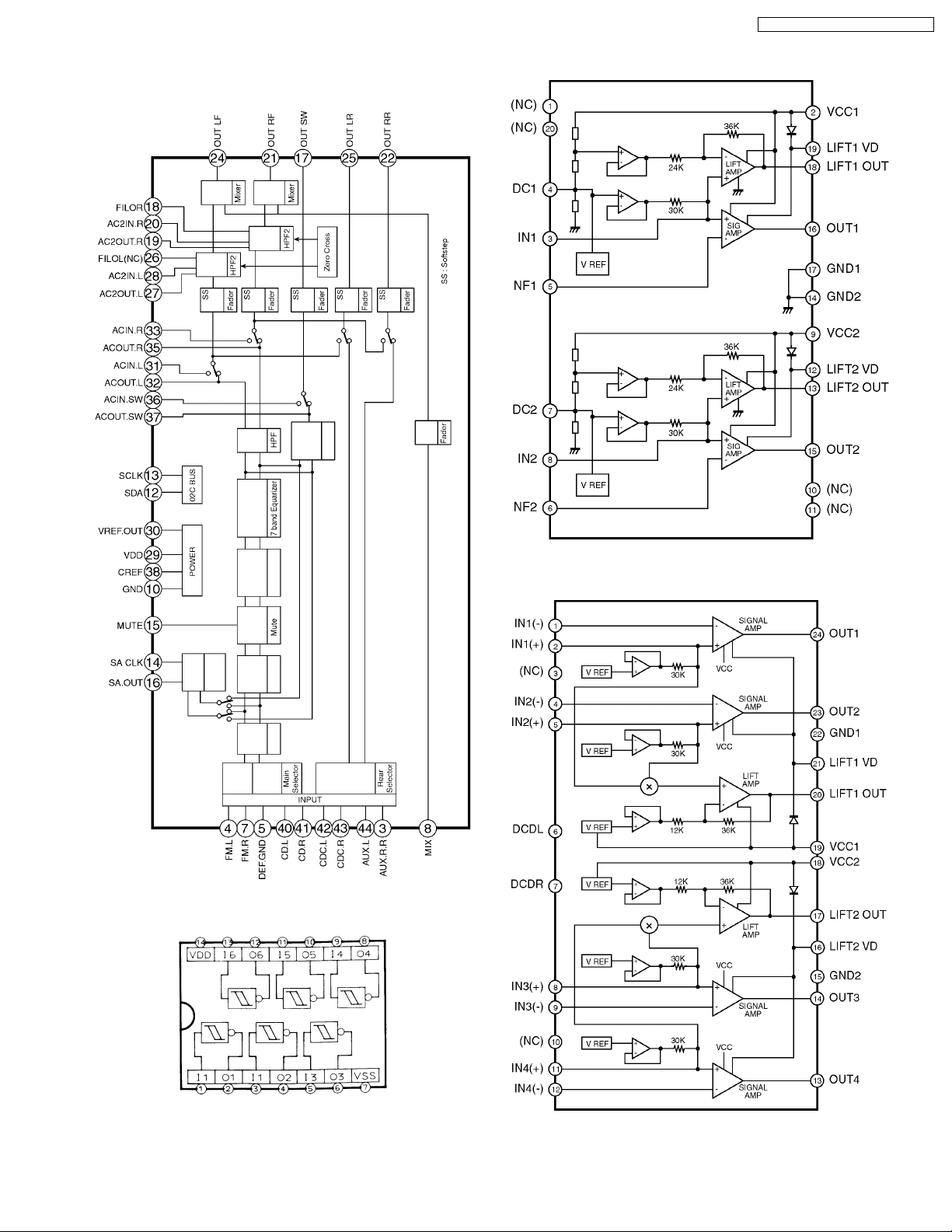
IC241 : C1BB00000650 (CQ-C8351N/C8301N)
IC251 : C1BB00000649 (CQ-C8351N/C8301N)
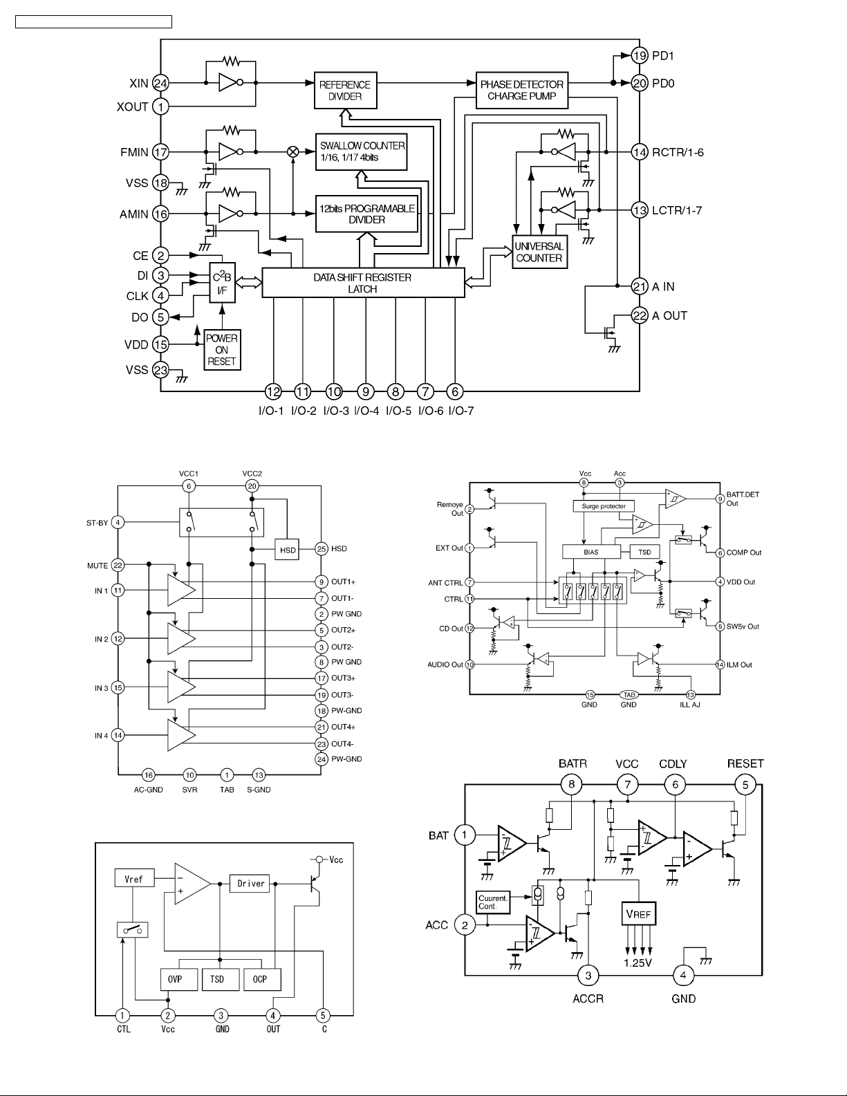
12 IC BLOCK DIAGRAM
17
CQ-C8351N / CQ-C8301N / CQ-C7301N
IC271 : C1EA00000043
IC730 : C0DAEKG00002
IC701 : C0DAZHF00004
IC702 : AN8065SE1
IC401 : C1BB00000644
18
CQ-C8351N / CQ-C8301N / CQ-C7301N
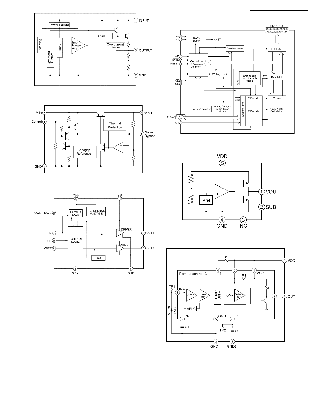
IC752 : C0CAABG00012
IC755 : C0DBZGD00040
IC760 : C0GBG0000032
12.2. Display Block
IC901 : MBM29V14N
IC902 : C0EBF0000374
IC903 : B3MBZ0000006
19
CQ-C8351N / CQ-C8301N / CQ-C7301N
 Loading...