

Motorola MC12018D, MC12018P Datasheet
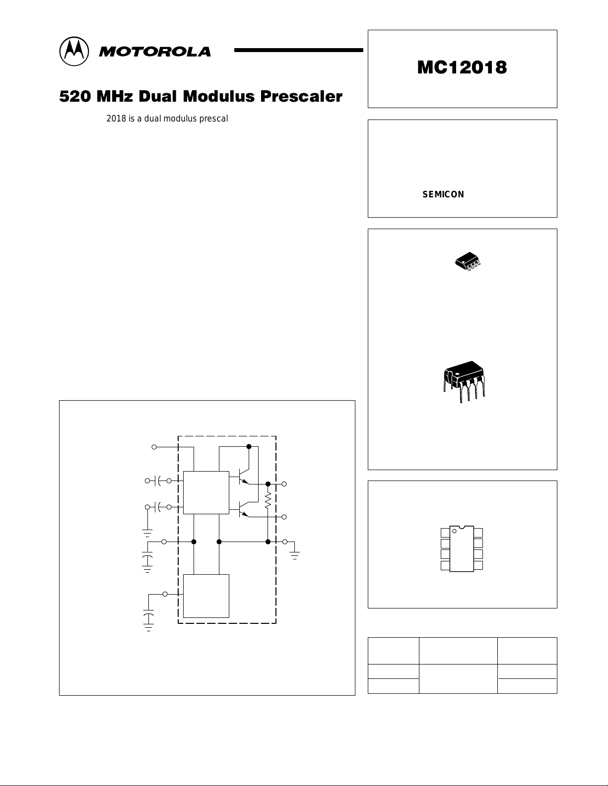
The MC12018 is a dual modulus prescaler which divides by 128 and 129.
An internal regulator is provided to allow this device to be used over a wide
range of power supply voltages. The devices may be operated by applying a
supply voltage of 5.0 Vdc ±10% at Pin 7, or by applying an unregulated
voltage source from 5.5 Vdc to 9.5 Vdc to Pin 8.
• 520 MHz Toggle Frequency
• Low–Power 8.0 mA Typical
• Control Input Is Compatible With Standard CMOS and TTL
• Supply Voltage 4.5 V to 9.5 V
• On–Chip 10 kΩ Resistor from Positive Edge to Ground
Order this document by MC12018/D
MECL PLL COMPONENTS
÷128/129 DUAL MODULUS
PRESCALER
SEMICONDUCTOR
TECHNICAL DATA
8
1
D SUFFIX
PLASTIC PACKAGE
CASE 751
(SO–8)
SIMPLIFIED BLOCK DIAGRAM
Control
Input
1
0.001 µF
Signal
Input
Signal
Gnd
1. V
2. Pin 7 is not to be used as a source of regulated output
3. 10 k
5
6
0.001 µF
V
reg
7
0.1 µF
V
CC
8
0.1 µF
at Pin 7 is not guaranteed to be between 4.5 and
reg
5.5 V when VCC is being applied to Pin 8
voltage
Ω
pulldown recommended with negative edge
output (Pin 2)
reg
TO V
÷
N / N+1
Voltage
Regulator
3
10 k
2
4
POS
Edge
NEG
Edge
Gnd
ORDERING INFORMATION
Device
MC12018D
MC12018P
8
1
P SUFFIX
PLASTIC PACKAGE
CASE 626
PIN CONNECTIONS
(Top View)
8
V
CC
7
V
reg
6
S
Gnd
5
S
IN
1
IN
2
NE
3
PE
4
Gnd
Operating
Temperature Range
TA = – 40° to +85°C
Package
SO–8
Plastic
Motorola, Inc. 1997 Rev 2
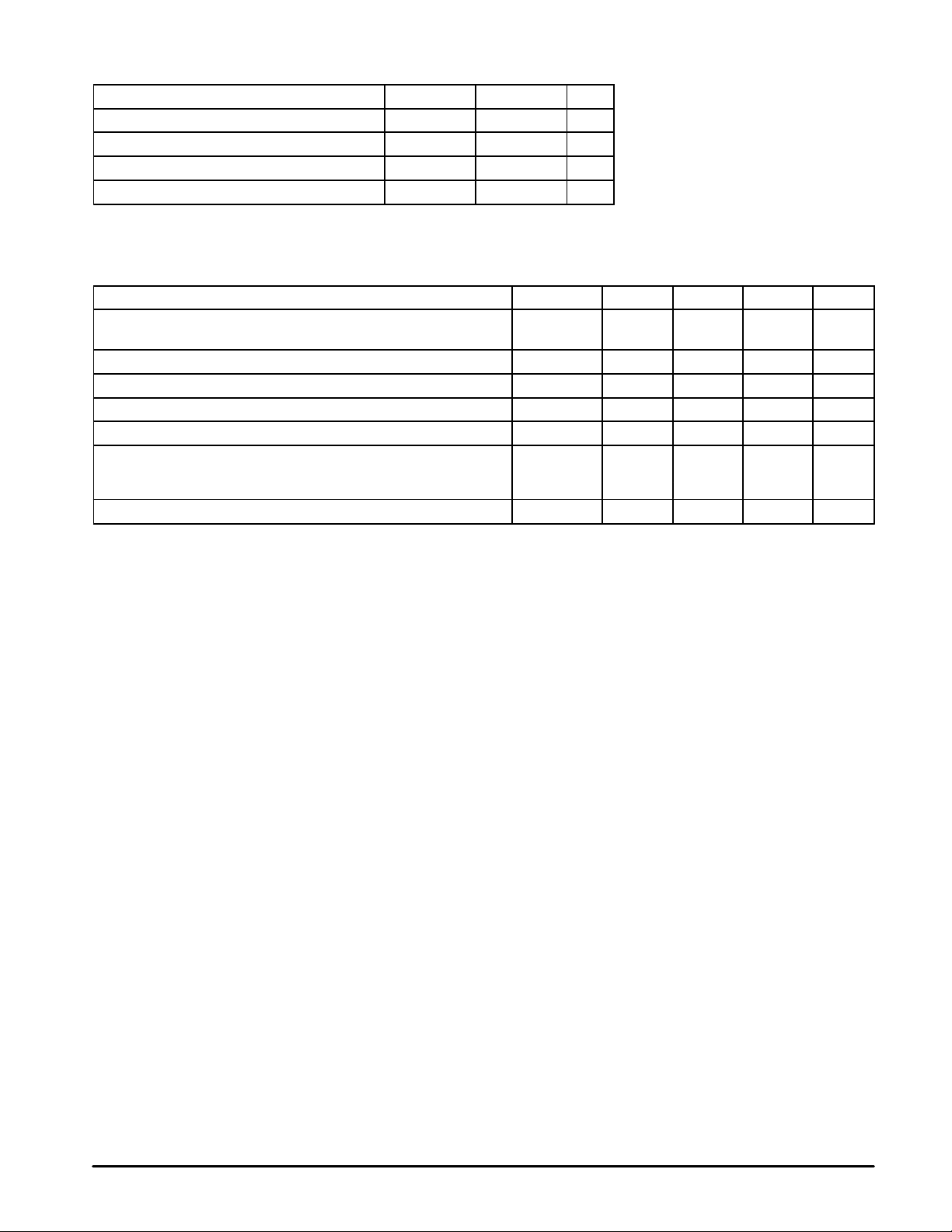
MAXIMUM RATINGS
Rating Symbol Value Unit
Regulated Voltage, Pin 7 V
Power Supply Voltage, Pin 8 V
Operating Temperature Range T
Storage Temperature Range T
NOTE; ESD data available upon request.
MC12018
reg
CC
A
stg
8.0 Vdc
10 Vdc
–40 to +85 °C
–65 to +175 °C
ELECTRICAL CHARACTERISTICS (V
Characteristic
Toggle Frequency (Sine Wave Input) f
Supply Current I
Control Input HIGH (÷128) V
Control Input LOW (÷129) V
Differntial Output Voltage (I
Input Voltage Sensitivity V
75MHz 400 – 800
125–520MHz 200 – 800
PLL Response Time (Notes 1 and 2) t
NOTES: 1. t
(50%) to ensure proper modulus selection.
= the period of time the PLL has from the prescaler rising output tranistion (50%) to the modulus control input edge transition
PLL
2.t
= period of output waveform.
out
= –200µA) V
source
= 5.5 to 9.5 V; V
CC
= 4.5 to 5.5 V; TA = –40 to 85°C), unless otherwise noted.)
reg
Symbol Min Typ Max Unit
max
f
min
CC
out
PLL
520
–
– 8.0 10.7 mA
IH
IL
in
2.0 – – V
– – 0.8 V
0.8 1.0 – V
– – t
–
–
–
75
–50 ns
out
MHz
mV
PP
2
MOTOROLA RF/IF DEVICE DATA
 Loading...