

Motorola MC100LVEL38DWR2, MC100LVEL38, MC100LVEL38DW, MC100EL38DW, MC100EL38DWR2 Datasheet
...
SEMICONDUCTOR TECHNICAL DATA
4–1
REV 1
Motorola, Inc. 1996
10/94
÷
÷
The MC100LVEL38 is a low skew ÷2, ÷4/6 clock generation chip
designed explicitly for low skew clock generation applications. The
MC100EL38 is pin and functionally equivalent to the MC100LVEL38 but
is specified for operation at the standard 100K ECL voltage supply. The
internal dividers are synchronous to each other, therefore, the common
output edges are all precisely aligned. The device can be driven by either
a differential or single-ended LVECL or, if positive power supplies are
used, LVPECL input signal. In addition, by using the VBB output, a
sinusoidal source can be AC coupled into the device (see Interfacing
section of the ECLinPS Data Book DL140/D). If a single-ended input is
to be used, the VBB output should be connected to the CLK
input and
bypassed to ground via a 0.01µF capacitor. The VBB output is designed to
act as the switching reference for the input of the LVEL38 under
single-ended input conditions, as a result, this pin can only source/sink up
to 0.5mA of current.
The common enable (EN
) is synchronous so that the internal dividers
will only be enabled/disabled when the internal clock is already in the
LOW state. This avoids any chance of generating a runt clock pulse on
the internal clock when the device is enabled/disabled as can happen
with an asynchronous control. An internal runt pulse could lead to losing
synchronization between the internal divider stages. The internal enable
flip-flop is clocked on the falling edge of the input clock, therefore, all
associated specification limits are referenced to the negative edge of the
clock input.
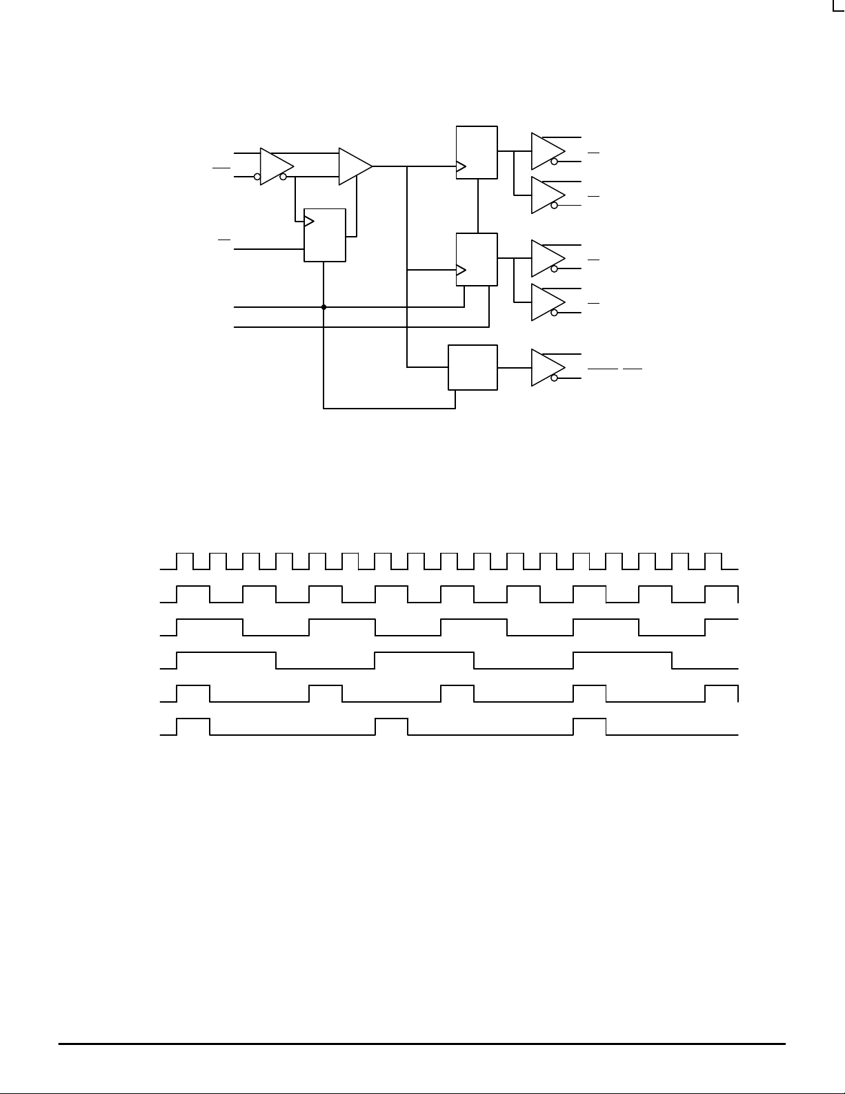
The Phase_Out output will go HIGH for one clock cycle whenever the
÷2 and the ÷4/6 outputs are both transitioning from a LOW to a HIGH.
This output allows for clock synchronization within the system.
Upon startup, the internal flip-flops will attain a random state; therefore,
for systems which utilize multiple LVEL38s, the master reset (MR) input
must be asserted to ensure synchronization. For systems which only use
one LVEL38, the MR pin need not be exercised as the internal divider
design ensures synchronization between the ÷2 and the ÷4/6 outputs of a
single device.
• 50ps Output-to-Output Skew
• Synchronous Enable/Disable
• Master Reset for Synchronization
• 75kΩ Internal Input Pulldown Resistors
• >1500V ESD Protection
• Low Voltage V
EE
Range of –3.0 to –3.8V
CLK
Pinout: 20-Lead SOIC (Top View)
CLK MR V
CC
1718 16 15 14 13 12
43
5 6 7 8 9
Q0
11
10
Q1 Q1 Q2 Q2 Q3 Q3 V
EE
EN
1920
21
VCCQ0
Phase_Out
Phase_Out
DIV_SEL V
BB
V
CC
DW SUFFIX
PLASTIC SOIC PACKAGE
CASE 751D-04
1
20
PIN FUNCTION
CLK Diff Clock Inputs
EN
Sync Enable
MR Master Reset
V
BB
Reference Output
Q0, Q
1
Diff ÷2 Outputs
Q2, Q
3
Diff ÷4/6 Outputs
DIVSEL Frequency Select Input
Phase_Out Phase Sync Signal
PIN DESCRIPTION
CLK
Z
ZZ
X
EN
L
H
X
MR
L
L
H
FUNCTION
Divide
Hold Q
0–3
Reset Q
0–3
FUNCTION TABLE
Z = Low-to-High Transition
ZZ = High-to-Low Transition
DIVSEL Q2, Q3 OUTPUTS
0 Divide by 4
1 Divide by 6
MC100LVEL38 MC100EL38
MOTOROLA ECLinPS and ECLinPS Lite
DL140 — Rev 3
4–2
Phase
Out
Logic
CLK
CLK
EN
MR
DIVSEL
÷
2
Q0
Q0
Q1
Q1
÷
4/6
Q2
Q2
Q3
Q3
PHASE_OUT
PHASE_OUT
LOGIC DIAGRAM
R
R
R
R
CLK
Q (
÷
2)
Q (
÷
4)
Q (
÷
6)
Phase_Out (
÷
4)
Phase_Out (
÷
6)
Figure 1. Timing Diagrams

MC100LVEL38 MC100EL38
4–3 MOTOROLAECLinPS and ECLinPS Lite
DL140 — Rev 3
MC100LVEL38
DC CHARACTERISTICS (VEE = –3.8V to –3.0; VCC = GND)
–40°C 0°C 25°C 85°C
Symbol Characteristic Min Typ Max Min Typ Max Min Typ Max Min Typ Max Unit
I
EE
Power Supply Current 50 60 50 60 50 60 54 65 mA
V
BB
Output Reference Voltage –1.38 –1.26 –1.38 –1.26 –1.38 –1.26 –1.38 –1.26 V
I
IH
Input High Current 150 150 150 150 µΑ
MC100LVEL38
AC CHARACTERISTICS (VEE = –3.8V to –3.0; VCC = GND)
–40°C 0°C 25°C 85°C
Symbol Characteristic Min Typ Max Min Typ Max Min Typ Max Min Typ Max Unit
f
MAX
Maximum Toggle Frequency 1000 1000 1000 1000 MHz
t
PLH
t
PHL
Propagation Delay CLK → Q (Diff)
to Output CLK → Q (S.E.)
CLK → Phase_Out (Diff)
CLK → Phase_Out (S.E.)
MR → Q
760
710
800
750
510
960
1010
1000
1050
810
780
730
820
770
530
980
1030
1020
1070
830
800
750
840
790
540
1000
1050
1040
1090
840
850
800
890
840
570
1050
1100
1090
1140
870
ps
t
SKEW
Within-Device Skew
1
Q0 – Q
3
All
50
75
50
75
50
75
5075ps
Part-to-Part Q0 – Q3 (Diff)
All
200
240
200
240
200
240
200
240
t
S
Setup Time EN → CLK
DIVSEL → CLK
150 150 150 150 ps
t
H
Hold Time CLK → EN
CLK → Div_Sel
150
200
150
200
150
200
150
200
ps
V
PP
2
Minimum Input Swing CLK 250 250 250 250 mV
V
CMR
3
Common Mode Range CLK –0.55 See3–0.55 See3–0.55 See3–0.55 See
3
V
t
RR
Reset Recovery Time 100 100 100 100 ps
t
PW
Minimum Pulse Width CLKMR800
700
800
700
800
700
800
700
ps
tr, t
f
Output Rise/Fall Times Q (20% – 80%) 280 550 280 550 280 550 280 550 ps
1. Skew is measured between outputs under identical transitions.
2. Minimum input swing for which AC parameters are guaranteed. The device will function reliably with differential inputs down to 100mV.
3. The CMR range is referenced to the most positive side of the differential input signal. Normal operation is obtained if the HIGH level falls within
the specified range and the peak-to-peak voltage lies between VPP
Min
and 1.0V . The lower end of the CMR range is dependent on VEE and
is equal to VEE + 1.65V.

MC100LVEL38 MC100EL38
MOTOROLA ECLinPS and ECLinPS Lite
DL140 — Rev 3
4–4
MC100EL38
DC CHARACTERISTICS (VEE = –4.2V to –5.46; VCC = GND)
–40°C 0°C 25°C 85°C
Symbol Characteristic Min Typ Max Min Typ Max Min Typ Max Min Typ Max Unit
I
EE
Power Supply Current 50 60 50 60 50 60 54 65 mA
V
BB
Output Reference Voltage –1.38 –1.26 –1.38 –1.26 –1.38 –1.26 –1.38 –1.26 V
I
IH
Input High Current 150 150 150 150 µΑ
MC100EL38
AC CHARACTERISTICS (VEE = –4.2V to –5.46; VCC = GND)
–40°C 0°C 25°C 85°C
Symbol Characteristic Min Typ Max Min Typ Max Min Typ Max Min Typ Max Unit
f
MAX
Maximum Toggle Frequency 1000 1000 1000 1000 MHz
t
PLH
t
PHL
Propagation Delay CLK → Q (Diff)
to Output CLK → Q (S.E.)
CLK → Phase_Out (Diff)
CLK → Phase_Out (S.E.)
MR → Q
760
710
800
750
510
960
1010
1000
1050
810
780
730
820
770
530
980
1030
1020
1070
830
800
750
840
790
540
1000
1050
1040
1090
840
850
800
890
840
570
1050
1100
1090
1140
870
ps
t
SKEW
Within-Device Skew
1
Q0 – Q
3
All
50
75
50
75
50
75
5075ps
Part-to-Part Q0 – Q3 (Diff)
All
200
240
200
240
200
240
200
240
t
S
Setup Time EN → CLK
DIVSEL → CLK
150 150 150 150 ps
t
H
Hold Time CLK → EN
CLK → Div_Sel
150
200
150
200
150
200
150
200
ps
V
PP
2
Minimum Input Swing CLK 250 250 250 250 mV
V
CMR
3
Common Mode Range CLK –0.55 See3–0.55 See3–0.55 See3–0.55 See
3
V
t
RR
Reset Recovery Time 100 100 100 100 ps
t
PW
Minimum Pulse Width CLKMR800
700
800
700
800
700
800
700
ps
tr, t
f
Output Rise/Fall Times Q (20% – 80%) 280 550 280 550 280 550 280 550 ps
1. Skew is measured between outputs under identical transitions.
2. Minimum input swing for which AC parameters are guaranteed. The device will function reliably with differential inputs down to 100mV.
3. The CMR range is referenced to the most positive side of the differential input signal. Normal operation is obtained if the HIGH level falls within
the specified range and the peak-to-peak voltage lies between VPP
Min
and 1.0V . The lower end of the CMR range is dependent on VEE and
is equal to VEE + 1.65V.

MC100LVEL38 MC100EL38
4–5 MOTOROLAECLinPS and ECLinPS Lite
DL140 — Rev 3
OUTLINE DIMENSIONS
DW SUFFIX
PLASTIC SOIC PACKAGE
CASE 751D–04
ISSUE E
MIN MINMAX MAX
MILLIMETERS INCHES
DIM
A
B
C
D
F
G
J
K
M
P
R
0.510
0.299
0.104
0.019
0.035
0.012
0.009
7
°
0.415
0.029
0.499
0.292
0.093
0.014
0.020
0.010
0.004
0
°
0.395
0.010
12.95
7.60
2.65
0.49
0.90
0.32
0.25
7
°
10.55
0.75
12.65
7.40
2.35
0.35
0.50
0.25
0.10
0
°
10.05
0.25
NOTES:
1. DIMENSIONING AND TOLERANCING PER
ANSI Y14.5M, 1982.
2. CONTROLLING DIMENSION: MILLIMETER.
3. DIMENSIONS A AND B DO NOT INCLUDE
MOLD PROTRUSION.
4. MAXIMUM MOLD PROTRUSION 0.150
(0.006) PER SIDE.
5. DIMENSION D DOES NOT INCLUDE
DAMBAR PROTRUSION. ALLOWABLE
DAMBAR PROTRUSION SHALL BE 0.13
(0.005) TOTAL IN EXCESS OF D DIMENSION
AT MAXIMUM MATERIAL CONDITION.
1.27 BSC 0.050 BSC
–A
–
–B
–
P 10 PL
1 10
1120
–T
–
D
20 PL
K
C
SEATING
PLANE
R X 45°
M
0.010 (0.25)
B
M M
0.010 (0.25) T A B
M
S S
G 18 PL
F
J
Motorola reserves the right to make changes without further notice to any products herein. Motorola makes no warranty , representation or guarantee regarding
the suitability of its products for any particular purpose, nor does Motorola assume any liability arising out of the application or use of any product or circuit, and
specifically disclaims any and all liability , including without limitation consequential or incidental damages. “Typical” parameters which may be provided in Motorola
data sheets and/or specifications can and do vary in different applications and actual performance may vary over time. All operating parameters, including “Typicals”
must be validated for each customer application by customer’s technical experts. Motorola does not convey any license under its patent rights nor the rights of
others. Motorola products are not designed, intended, or authorized for use as components in systems intended for surgical implant into the body, or other
applications intended to support or sustain life, or for any other application in which the failure of the Motorola product could create a situation where personal injury
or death may occur. Should Buyer purchase or use Motorola products for any such unintended or unauthorized application, Buyer shall indemnify and hold Motorola
and its officers, employees, subsidiaries, affiliates, and distributors harmless against all claims, costs, damages, and expenses, and reasonable attorney fees
arising out of, directly or indirectly, any claim of personal injury or death associated with such unintended or unauthorized use, even if such claim alleges that
Motorola was negligent regarding the design or manufacture of the part. Motorola and are registered trademarks of Motorola, Inc. Motorola, Inc. is an Equal
Opportunity/Affirmative Action Employer.
How to reach us:
USA/EUROPE/Locations Not Listed: Motorola Literature Distribution; JAPAN: Nippon Motorola Ltd.; Tatsumi–SPD–JLDC, 6F Seibu–Butsuryu–Center,
P.O. Box 20912; Phoenix, Arizona 85036. 1–800–441–2447 or 602–303–5454 3–14–2 Tatsumi Koto–Ku, Tokyo 135, Japan. 03–81–3521–8315
MFAX: RMFAX0@email.sps.mot.com – TOUCHTONE 602–244–6609 ASIA/PACIFIC: Motorola Semiconductors H.K. Ltd.; 8B Tai Ping Industrial Park,
INTERNET: http://Design–NET.com 51 Ting Kok Road, Tai Po, N.T., Hong Kong. 852–26629298
MC100LVEL38/D
*MC100LVEL38/D*
◊
 Loading...