

Motorola MC100LVEL33, MC100LVEL33D, MC100LVEL33DR2 Datasheet
MOTOROLA
SEMICONDUCTOR TECHNICAL DATA
3–1
REV 0
Motorola, Inc. 1996
8/96
÷
4 Divider
The MC100LVEL33 is an integrated ÷4 divider. The differential clock
inputs and the VBB allow a differential, single-ended or AC coupled
interface to the device. If used, the VBB output should be bypassed to
ground with a 0.01µF capacitor. Also note that the VBB is designed to be
used as an input bias on the EL33 only , the VBB output has limited current
sink and source capability. The LVEL is functionally equivalent to the
EL33 and works from a low voltage supply.
The reset pin is asynchronous and is asserted on the rising edge.
Upon power-up, the internal flip-flops will attain a random state; the reset
allows for the synchronization of multiple LVEL33’s in a system.
• 630ps Propagation Delay
• 4.0GHz Toggle Frequency
• High Bandwidth Output Transitions
• Operates from –3.3V (or 3.3V) Supply
• 75kΩ Internal Input Pulldown Resistors
• >2000V ESD Protection
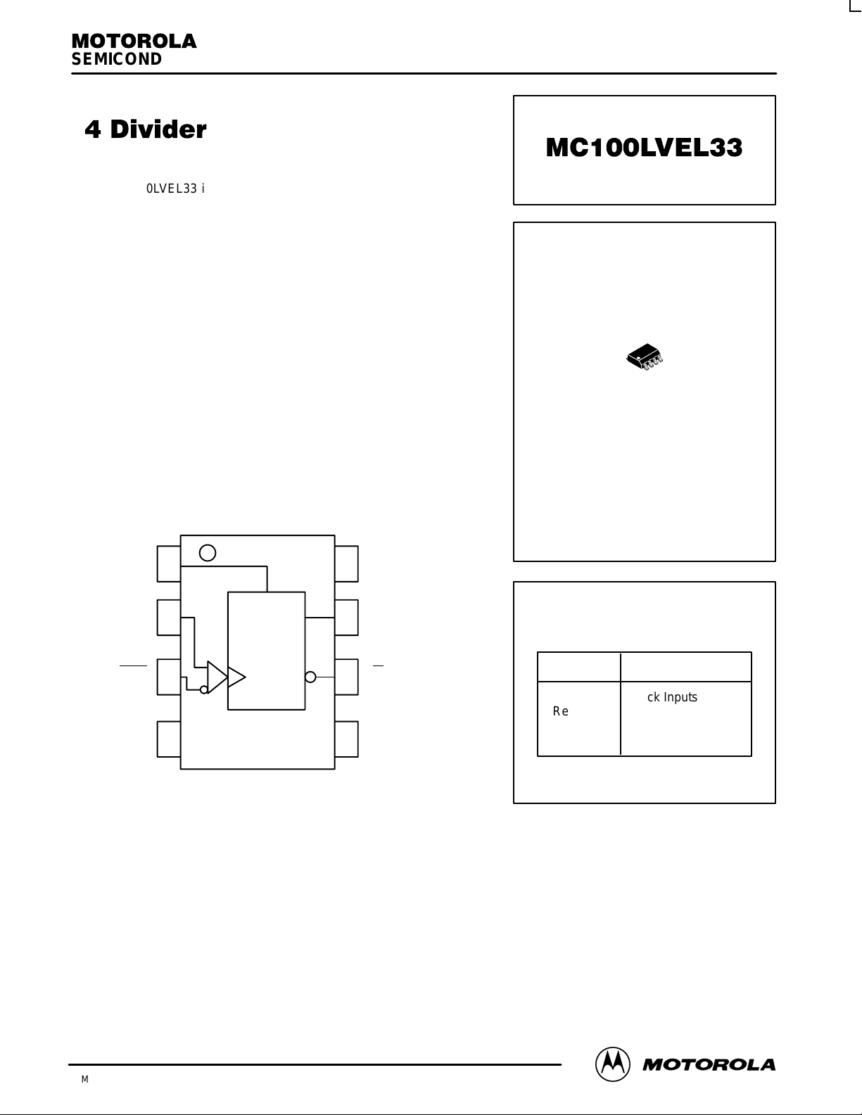
LOGIC DIAGRAM AND PINOUT ASSIGNMENT
4
3
1
2
5
6
78Q
V
EE
V
CC
QCLK
V
BB
R
÷4
Reset
CLK
MC100LVEL33
PIN FUNCTION
CLK Clock Inputs
Reset Asynch Reset
V
BB
Ref Voltage Output
Q Data Ouputs
PIN DESCRIPTION
1
8
D SUFFIX
PLASTIC SOIC PACKAGE
CASE 751-05
MC100LVEL33
MOTOROLA ECLinPS and ECLinPS Lite
DL140 — Rev 3
3–2
DC CHARACTERISTICS (VEE = VEE(min) to VEE(max); VCC = GND)
–40°C 0°C 25°C 85°C
Symbol Characteristic Min Typ Max Min Typ Max Min Typ Max Min Typ Max Unit
I
EE
Power Supply Current 33 37 33 37 33 37 35 39 mA
V
EE
Power Supply Voltage –3.0 –3.8 –3.0 –3.8 –3.0 –3.8 –3.0 –3.8 V
V
BB
Output Reference Voltage –1.38 –1.26 –1.38 –1.26 –1.38 –1.26 –1.38 –1.26 V
I
IH
Input HIGH Current 150 150 150 150 µA
I
IL
Input LOW Current CLK
Other
–600
0.5
–600
0.5
–600
0.5
–600
0.5
µA
AC CHARACTERISTICS (VEE = VEE(min) to VEE(max); VCC = GND)
–40°C 0°C 25°C 85°C
Symbol Characteristic Min Typ Max Min Typ Max Min Typ Max Min Typ Max Unit
f
MAX
Maximum Toggle
Frequency
3.4 4.2 3.8 4.2 3.8 4.2 3.8 4.2 GHz
t
PLH
t
PHL
Propagation Delay
CLK to Q (Diff)
CLK to Q (SE)
Reset to Q
510
460
500
690
740
700
530
480
510
710
760
710
540
490
520
720
770
720
600
550
580
780
830
780
ps
t
rr
Reset Recovery 300 300 300 300 ps
t
skew
Duty Cycle Skew
2
20 20 20 20 ps
V
PP
Minimum Input Swing
1
150 150 150 150 mV
V
CMR
Common Mode Range
3
VPP < 500mV
VPP ≥ 500mV
–2.0
–1.8
–0.4
–0.4
–2.1
–1.9
–0.4
–0.4
–2.1
–1.9
–0.4
–0.4
–2.1
–1.9
–0.4
–0.4
V
t
r
t
f
Output Rise/Fall Times Q
(20% – 80%)
120 320 120 320 120 320 120 320 ps
1. Minimum input swing for which AC parameters are guaranteed.
2. Duty cycle skew is the difference between T
PLH
and T
PLL
.
3. The CMR range is referenced to the most positive side of the differential input signal. Normal operation is obtained if the HIGH level falls within
the specified range and the peak-to-peak voltage lies between VPPmin and 1V. The lower end of the CMR range varies 1:1 with VEE. The
numbers in the spec table assume a nominal VEE = –3.3V. Note for PECL operation, the V
CMR
(min) will be fixed at 3.3V – |V
CMR
(min)|.
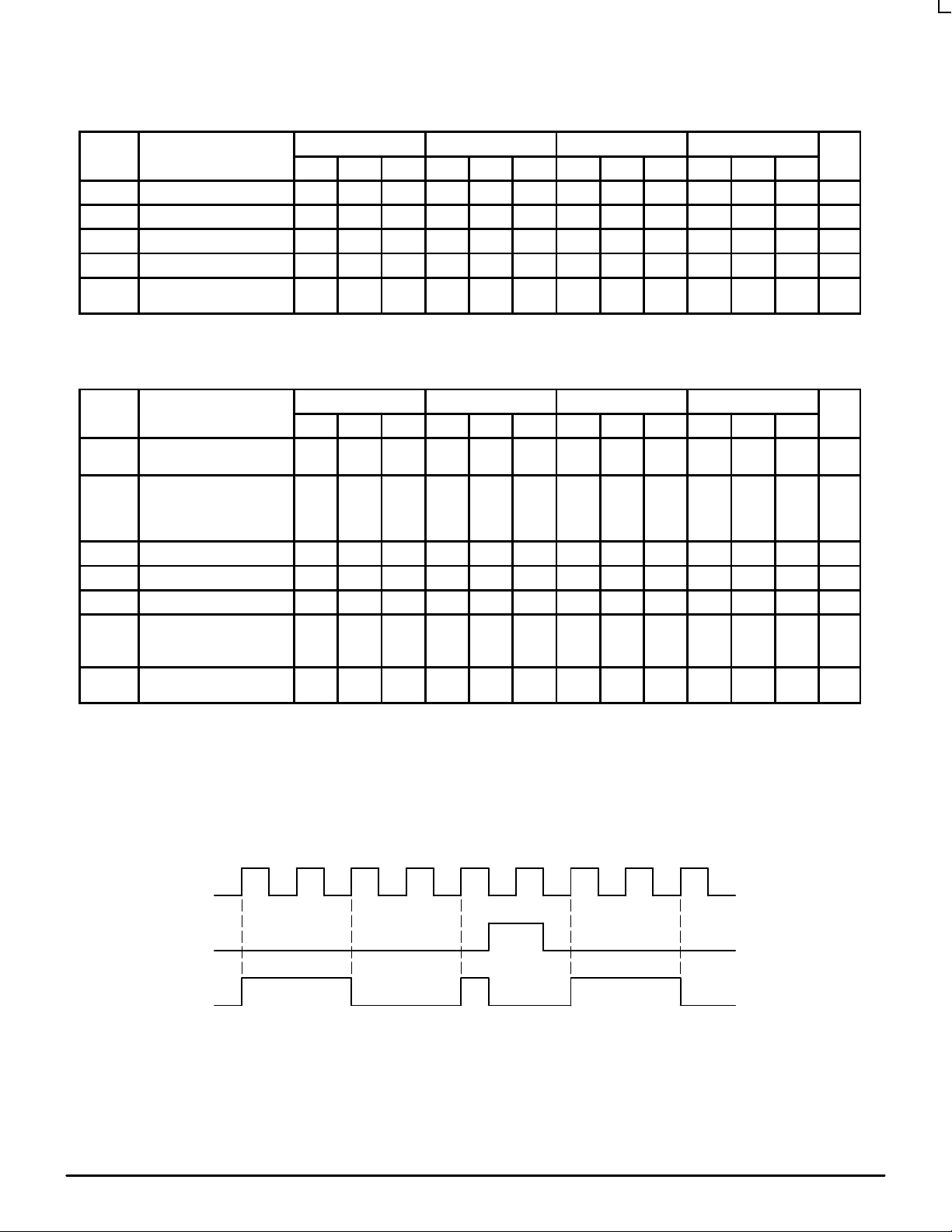
Figure 1. Timing Diagram
CLK
RESET
Q
 Loading...