

MOTOROLA MC100LVEL32DR2, MC100LVEL32D Datasheet
MC100LVEL32
÷
2 Divider
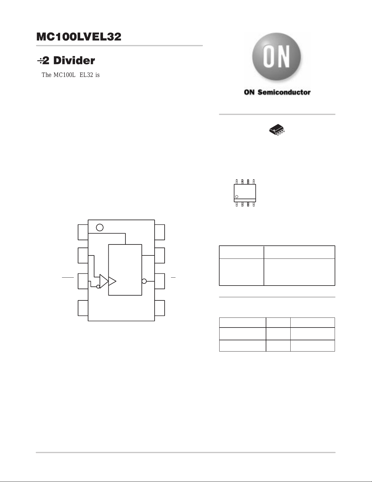
The MC100LVEL32 is an integrated ÷2 divider. The differential
clock inputs and the VBB allow a differential, single-ended or AC
coupled interface to the device. If used, the VBB output should be
bypassed to ground with a 0.01µF capacitor . Also note that the VBB is
designed to be used as an input bias on the LVEL32 only, the V
output has limited current sink and source capability.The LVEL32 is
functionally identical to the EL32, but operates from a low voltage
supply.
The reset pin is asynchronous and is asserted on the rising edge.
Upon power-up, the internal flip-flop will attain a random state; the
reset allows for the synchronization of multiple EL32’s in a system.
• 510ps Propagation Delay
• 3.0GHz T oggle Frequency
• High Bandwidth Output Transitions
• 75kΩ Internal Input Pulldown Resistors
• >1000V ESD Protection
LOGIC DIAGRAM AND PINOUT ASSIGNMENT
Reset
CLK
1
R
2
÷2
3
78Q
6
V
CC
QCLK
BB
http://onsemi.com
8
1
SO–8
D SUFFIX
CASE 751
MARKING DIAGRAM
8
KVL32
ALYW
1
*For additional information, see Application Note
AND8002/D
PIN FUNCTION
CLK Clock Inputs
Reset Asynch Reset
V
BB
Q Data Ouputs
A = Assembly Location
L = Wafer Lot
Y = Year
W = Work Week
PIN DESCRIPTION
Ref Voltage Output
BB
4
V
Semiconductor Components Industries, LLC, 2000
April, 2000 – Rev. 1
5
V
EE
MC100L VEL32D SO–8 98 Units/Rail
MC100L VEL32DR2 SO–8 2500 Tape & Reel
1 Publication Order Number:
ORDERING INFORMATION
Device Package Shipping
MC100L VEL32/D
MC100LVEL32
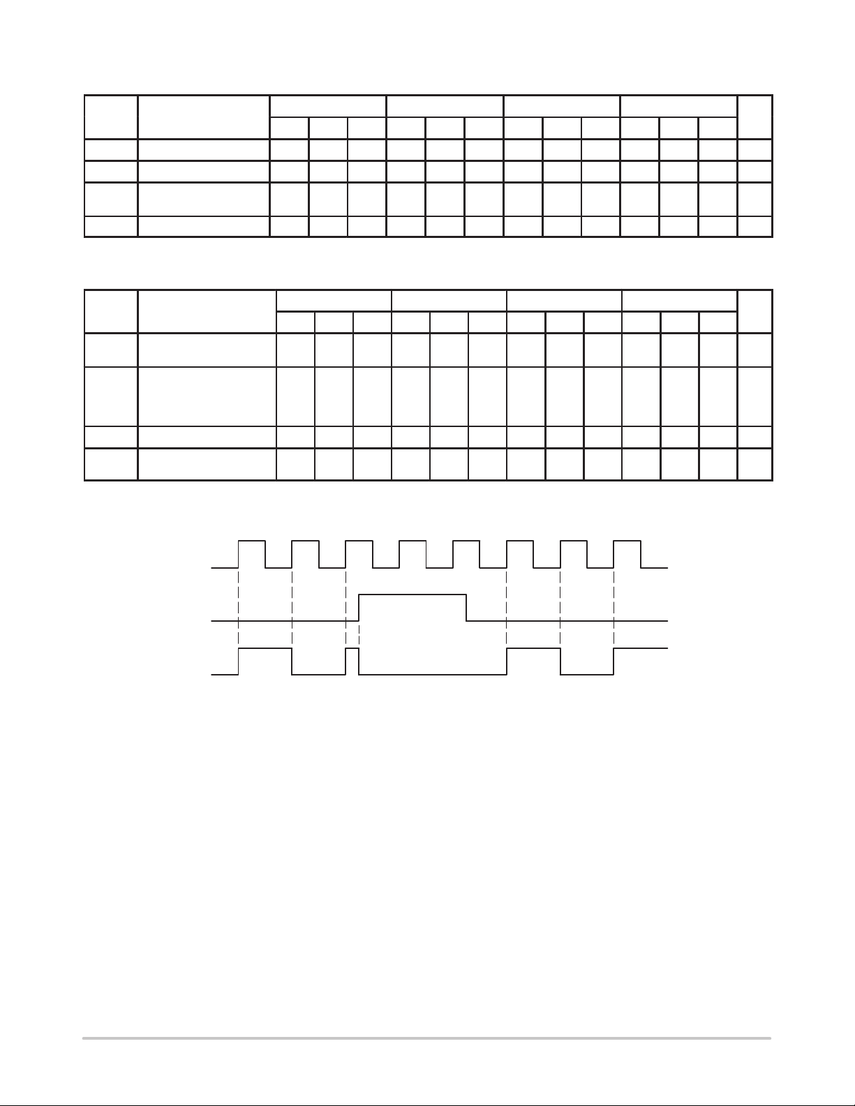
DC CHARACTERISTICS (VEE = VEE(min) to VEE(max); VCC = GND)
–40°C 0°C 25°C 85°C
Symbol Characteristic Min Typ Max Min Typ Max Min Typ Max Min Typ Max Unit
I
EE
V
EE
V
BB
I
IH
AC CHARACTERISTICS (VEE = VEE(min) to VEE(max); VCC = GND)
Symbol Characteristic Min Typ Max Min Typ Max Min Typ Max Min Typ Max Unit
f
MAX
t
PLH
t
PHL
V
PP
t
r
t
f
1. Minimum input swing for which AC parameters are guaranteed.
Power Supply Current 25 25 25 25 mA
Power Supply Voltage –3.0 –3.0 –3.3 –3.8 –3.0 –3.3 –3.8 –3.0 –3.3 –3.8 V
Output Reference
Voltage
Input HIGH Current 150 150 150 150 µA
Maximum Toggle
Frequency
Propagation Delay
CLK to Q (Diff)
CLK to Q (S.E.)
Reset to Q
Minimum Input Swing
Output Rise/Fall Times Q
(20% – 80%)
–1.38 –1.26 –1.38 –1.26 –1.38 –1.26 –1.38 –1.26 V
–40°C 0°C 25°C 85°C
3.0 3.0 3.0 3.0 GHz
350
500
530
360
500
540
370
510
550
410
300
500
580
310
500
590
320
510
340
540
540
350
540
550
350
1
150 150 150 150 mV
225 225 225 225 ps
540
600
550
360
380
540
540
550
590
640
580
ps
CLK
RESET
Q
Figure 1. Timing Diagram
http://onsemi.com
2
 Loading...