

Motorola MC100LVEL32 Datasheet
MC100LVEL32
PIN FUNCTION
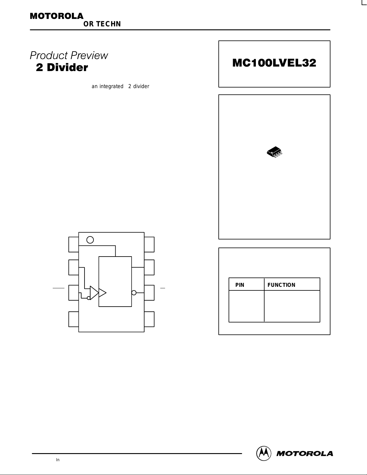
CLK Clock Inputs
Reset Asynch Reset
V
BB
Ref Voltage Output
Q Data Ouputs
PIN DESCRIPTION
1
8
D SUFFIX
PLASTIC SOIC PACKAGE
CASE 751-05
MOTOROLA
SEMICONDUCTOR TECHNICAL DATA
4–1
REV 0
Motorola, Inc. 1996
5/96
÷
2 Divider
The MC100LVEL32 is an integrated ÷2 divider. The differential clock
inputs and the VBB allow a differential, single-ended or AC coupled
interface to the device. If used, the VBB output should be bypassed to
ground with a 0.01µF capacitor. Also note that the VBB is designed to be
used as an input bias on the LVEL32 only, the VBB output has limited
current sink and source capability.The LVEL32 is functionally identical to
the EL32, but operates from a low voltage supply.
The reset pin is asynchronous and is asserted on the rising edge.
Upon power-up, the internal flip-flop will attain a random state; the reset
allows for the synchronization of multiple EL32’s in a system.
• 510ps Propagation Delay
• 3.0GHz Toggle Frequency
• High Bandwidth Output Transitions
• 75kΩ Internal Input Pulldown Resistors
• >1000V ESD Protection
1
2
5
6
78Q
V
EE
V
CC
QCLK
V
BB
R
÷2
Reset
CLK
This document contains information on a product under development. Motorola reserves the right to change or
discontinue this product without notice.
LOGIC DIAGRAM AND PINOUT ASSIGNMENT
3
4
MC100LVEL32
MOTOROLA ECLinPS and ECLinPS Lite
DL140 — Rev 3
4–2
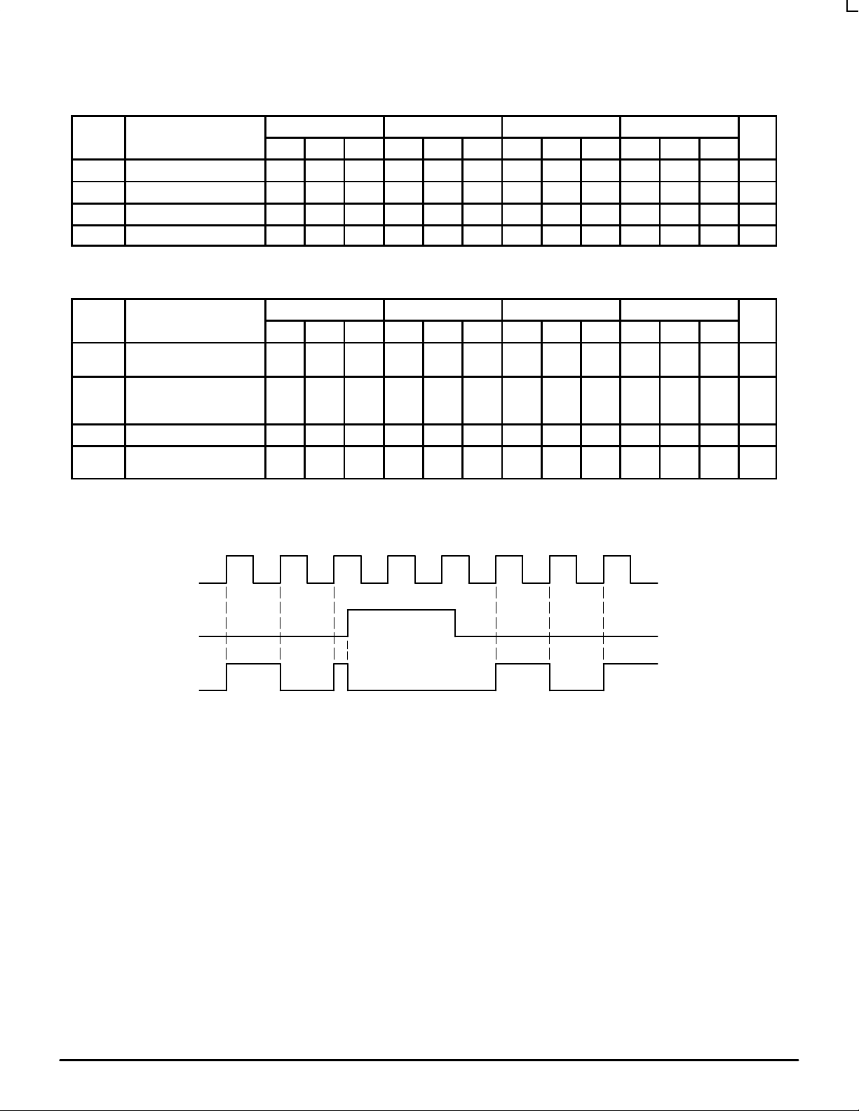
DC CHARACTERISTICS (VEE = VEE(min) to VEE(max); VCC = GND)
–40°C 0°C 25°C 85°C
Symbol Characteristic Min Typ Max Min Typ Max Min Typ Max Min Typ Max Unit
I
EE
Power Supply Current 25 25 25 25 mA
V
EE
Power Supply Voltage –3.0 –3.0 –3.3 –3.8 –3.0 –3.3 –3.8 –3.0 –3.3 –3.8 V
V
BB
Output Reference Voltage –1.38 –1.26 –1.38 –1.26 –1.38 –1.26 –1.38 –1.26 V
I
IH
Input HIGH Current 150 150 150 150 µA
AC CHARACTERISTICS (VEE = VEE(min) to VEE(max); VCC = GND)
–40°C 0°C 25°C 85°C
Symbol Characteristic Min Typ Max Min Typ Max Min Typ Max Min Typ Max Unit
f
MAX
Maximum Toggle
Frequency
3.0 3.0 3.0 3.0 GHz
t
PLH
t
PHL
Propagation Delay
CLK to Q
Reset to Q
500
540
500
540
510
540
540
550
ps
V
PP
Minimum Input Swing
1
150 150 150 150 mV
t
r
t
f
Output Rise/Fall Times Q
(20% – 80%)
225 225 225 225 ps
1. Minimum input swing for which AC parameters are guaranteed.
Figure 1. Timing Diagram
CLK
RESET
Q
 Loading...