


47LD455B-CA
LCD TV
SERVICE MANUAL
CAUTION
BEFORE SERVICING THE CHASSIS,
READ THE SAFETY PRECAUTIONS IN THIS MANUAL.
CHASSIS : LC01W
MODEL : 47LD455B 47LD455B-CA
MODEL : 47LD455H
47LD455H-CA
North/Latin America http://aic.lgservice.com
Europe/Africa http://eic.lgservice.com
Asia/Oceania http://biz.lgservice.com
Internal Use Only
Printed in KoreaP/NO : MFL62864856 (1105-REV00)

LGE Internal Use OnlyCopyright © 2011 LG Electronics. Inc. All right reserved.
Only for training and service purposes
- 2 -
CONTENTS
CONTENTS .............................................................................................. 2
PRODUCT SAFETY ................................................................................. 3
SPECIFICATION ....................................................................................... 6
ADJUSTMENT INSTRUCTION ................................................................ 8
BLOCK DIAGRAM.................................................................................. 13
EXPLODED VIEW .................................................................................. 15
SCHEMATIC CIRCUIT DIAGRAM ..............................................................
LGE Internal Use OnlyCopyright © 2011 LG Electronics. Inc. All right reserved.
Only for training and service purposes
- 3 -
SAFETY PRECAUTIONS
Many electrical and mechanical parts in this chassis have special safety-related characteristics. These parts are identified by in the
Schematic Diagram and Exploded View.
It is essential that these special safety parts should be replaced with the same components as recommended in this manual to prevent
Shock, Fire, or other Hazards.
Do not modify the original design without permission of manufacturer.
General Guidance
An isolation Transformer should always be used during the
servicing of a receiver whose chassis is not isolated from the AC
power line. Use a transformer of adequate power rating as this
protects the technician from accidents resulting in personal injury
from electrical shocks.
It will also protect the receiver and it's components from being
damaged by accidental shorts of the circuitry that may be
inadvertently introduced during the service operation.
If any fuse (or Fusible Resistor) in this TV receiver is blown,
replace it with the specified.
When replacing a high wattage resistor (Oxide Metal Film Resistor,
over 1 W), keep the resistor 10mm away from PCB.
Keep wires away from high voltage or high temperature parts.
Before returning the receiver to the customer,
always perform an AC leakage current check on the exposed
metallic parts of the cabinet, such as antennas, terminals, etc., to
be sure the set is safe to operate without damage of electrical
shock.
Leakage Current Cold Check(Antenna Cold Check)
With the instrument AC plug removed from AC source, connect an
electrical jumper across the two AC plug prongs. Place the AC
switch in the on position, connect one lead of ohm-meter to the AC
plug prongs tied together and touch other ohm-meter lead in turn to
each exposed metallic parts such as antenna terminals, phone
jacks, etc.
If the exposed metallic part has a return path to the chassis, the
measured resistance should be between 1 MΩ and 5.2 MΩ.
When the exposed metal has no return path to the chassis the
reading must be infinite.
An other abnormality exists that must be corrected before the
receiver is returned to the customer.
Leakage Current Hot Check (See below Figure)
Plug the AC cord directly into the AC outlet.
Do not use a line Isolation Transformer during this check.
Connect 1.5 K / 10 watt resistor in parallel with a 0.15 uF capacitor
between a known good earth ground (Water Pipe, Conduit, etc.)
and the exposed metallic parts.
Measure the AC voltage across the resistor using AC voltmeter
with 1000 ohms/volt or more sensitivity.
Reverse plug the AC cord into the AC outlet and repeat AC voltage
measurements for each exposed metallic part. Any voltage
measured must not exceed 0.75 volt RMS which is corresponds to
0.5 mA.
In case any measurement is out of the limits specified, there is
possibility of shock hazard and the set must be checked and
repaired before it is returned to the customer.
Leakage Current Hot Check circuit
1.5 Kohm/10W
To Instrument's
exposed
METALLIC PARTS
Good Earth Ground
such as WATER PIPE,
CONDUIT etc.
AC Volt-meter
When 25A is impressed between Earth and 2nd Ground
for 1 second, Resistance must be less than 0.1
*Base on Adjustment standard
IMPORTANT SAFETY NOTICE
0.15 uF
Ω

LGE Internal Use OnlyCopyright © 2011 LG Electronics. Inc. All right reserved.
Only for training and service purposes
- 4 -
CAUTION: Before servicing receivers covered by this service
manual and its supplements and addenda, read and follow the
SAFETY PRECAUTIONS on page 3 of this publication.
NOTE: If unforeseen circumstances create conflict between the
following servicing precautions and any of the safety precautions on
page 3 of this publication, always follow the safety precautions.
Remember: Safety First.
General Servicing Precautions
1. Always unplug the receiver AC power cord from the AC power
source before;
a. Removing or reinstalling any component, circuit board
module or any other receiver assembly.
b. Disconnecting or reconnecting any receiver electrical plug or
other electrical connection.
c. Connecting a test substitute in parallel with an electrolytic
capacitor in the receiver.
CAUTION: A wrong part substitution or incorrect polarity
installation of electrolytic capacitors may result in an
explosion hazard.
2. Test high voltage only by measuring it with an appropriate high
voltage meter or other voltage measuring device (DVM,
FETVOM, etc) equipped with a suitable high voltage probe.
Do not test high voltage by "drawing an arc".
3. Do not spray chemicals on or near this receiver or any of its
assemblies.
4. Unless specified otherwise in this service manual, clean
electrical contacts only by applying the following mixture to the
contacts with a pipe cleaner, cotton-tipped stick or comparable
non-abrasive applicator; 10 % (by volume) Acetone and 90 %
(by volume) isopropyl alcohol (90 % - 99 % strength)
CAUTION: This is a flammable mixture.
Unless specified otherwise in this service manual, lubrication of
contacts in not required.
5. Do not defeat any plug/socket B+ voltage interlocks with which
receivers covered by this service manual might be equipped.
6. Do not apply AC power to this instrument and/or any of its
electrical assemblies unless all solid-state device heat sinks are
correctly installed.
7. Always connect the test receiver ground lead to the receiver
chassis ground before connecting the test receiver positive
lead.
Always remove the test receiver ground lead last.
8. Use with this receiver only the test fixtures specified in this
service manual.
CAUTION: Do not connect the test fixture ground strap to any
heat sink in this receiver.
Electrostatically Sensitive (ES) Devices
Some semiconductor (solid-state) devices can be damaged easily
by static electricity. Such components commonly are called
Electrostatically Sensitive (ES) Devices. Examples of typical ES
devices are integrated circuits and some field-effect transistors and
semiconductor "chip" components. The following techniques
should be used to help reduce the incidence of component
damage caused by static by static electricity.
1. Immediately before handling any semiconductor component or
semiconductor-equipped assembly, drain off any electrostatic
charge on your body by touching a known earth ground.
Alternatively, obtain and wear a commercially available
discharging wrist strap device, which should be removed to
prevent potential shock reasons prior to applying power to the
unit under test.
2. After removing an electrical assembly equipped with ES
devices, place the assembly on a conductive surface such as
aluminum foil, to prevent electrostatic charge buildup or
exposure of the assembly.
3. Use only a grounded-tip soldering iron to solder or unsolder ES
devices.
4. Use only an anti-static type solder removal device. Some solder
removal devices not classified as "anti-static" can generate
electrical charges sufficient to damage ES devices.
5. Do not use freon-propelled chemicals. These can generate
electrical charges sufficient to damage ES devices.
6. Do not remove a replacement ES device from its protective
package until immediately before you are ready to install it.
(Most replacement ES devices are packaged with leads
electrically shorted together by conductive foam, aluminum foil
or comparable conductive material).
7. Immediately before removing the protective material from the
leads of a replacement ES device, touch the protective material
to the chassis or circuit assembly into which the device will be
installed.
CAUTION: Be sure no power is applied to the chassis or circuit,
and observe all other safety precautions.
8. Minimize bodily motions when handling unpackaged
replacement ES devices. (Otherwise harmless motion such as
the brushing together of your clothes fabric or the lifting of your
foot from a carpeted floor can generate static electricity
sufficient to damage an ES device.)
General Soldering Guidelines
1. Use a grounded-tip, low-wattage soldering iron and appropriate
tip size and shape that will maintain tip temperature within the
range or 500
°
F to 600 °F.
2. Use an appropriate gauge of RMA resin-core solder composed
of 60 parts tin/40 parts lead.
3. Keep the soldering iron tip clean and well tinned.
4. Thoroughly clean the surfaces to be soldered. Use a mall wirebristle (0.5 inch, or 1.25 cm) brush with a metal handle.
Do not use freon-propelled spray-on cleaners.
5. Use the following unsoldering technique
a. Allow the soldering iron tip to reach normal temperature.
(500
°F to 600 °F)
b. Heat the component lead until the solder melts.
c. Quickly draw the melted solder with an anti-static, suction-
type solder removal device or with solder braid.
CAUTION: Work quickly to avoid overheating the circuit
board printed foil.
6. Use the following soldering technique.
a. Allow the soldering iron tip to reach a normal temperature
(500
°F to 600 °F)
b. First, hold the soldering iron tip and solder the strand against
the component lead until the solder melts.
c. Quickly move the soldering iron tip to the junction of the
component lead and the printed circuit foil, and hold it there
only until the solder flows onto and around both the
component lead and the foil.
CAUTION: Work quickly to avoid overheating the circuit
board printed foil.
d. Closely inspect the solder area and remove any excess or
splashed solder with a small wire-bristle brush.
SERVICING PRECAUTIONS

LGE Internal Use OnlyCopyright © 2011 LG Electronics. Inc. All right reserved.
Only for training and service purposes
- 5 -
IC Remove/Replacement
Some chassis circuit boards have slotted holes (oblong) through
which the IC leads are inserted and then bent flat against the
circuit foil. When holes are the slotted type, the following technique
should be used to remove and replace the IC. When working with
boards using the familiar round hole, use the standard technique
as outlined in paragraphs 5 and 6 above.
Removal
1. Desolder and straighten each IC lead in one operation by gently
prying up on the lead with the soldering iron tip as the solder
melts.
2. Draw away the melted solder with an anti-static suction-type
solder removal device (or with solder braid) before removing the
IC.
Replacement
1. Carefully insert the replacement IC in the circuit board.
2. Carefully bend each IC lead against the circuit foil pad and
solder it.
3. Clean the soldered areas with a small wire-bristle brush.
(It is not necessary to reapply acrylic coating to the areas).
"Small-Signal" Discrete Transistor
Removal/Replacement
1. Remove the defective transistor by clipping its leads as close as
possible to the component body.
2. Bend into a "U" shape the end of each of three leads remaining
on the circuit board.
3. Bend into a "U" shape the replacement transistor leads.
4. Connect the replacement transistor leads to the corresponding
leads extending from the circuit board and crimp the "U" with
long nose pliers to insure metal to metal contact then solder
each connection.
Power Output, Transistor Device
Removal/Replacement
1. Heat and remove all solder from around the transistor leads.
2. Remove the heat sink mounting screw (if so equipped).
3. Carefully remove the transistor from the heat sink of the circuit
board.
4. Insert new transistor in the circuit board.
5. Solder each transistor lead, and clip off excess lead.
6. Replace heat sink.
Diode Removal/Replacement
1. Remove defective diode by clipping its leads as close as
possible to diode body.
2. Bend the two remaining leads perpendicular y to the circuit
board.
3. Observing diode polarity, wrap each lead of the new diode
around the corresponding lead on the circuit board.
4. Securely crimp each connection and solder it.
5. Inspect (on the circuit board copper side) the solder joints of
the two "original" leads. If they are not shiny, reheat them and if
necessary, apply additional solder.
Fuse and Conventional Resistor
Removal/Replacement
1. Clip each fuse or resistor lead at top of the circuit board hollow
stake.
2. Securely crimp the leads of replacement component around
notch at stake top.
3. Solder the connections.
CAUTION: Maintain original spacing between the replaced
component and adjacent components and the circuit board to
prevent excessive component temperatures.
Circuit Board Foil Repair
Excessive heat applied to the copper foil of any printed circuit
board will weaken the adhesive that bonds the foil to the circuit
board causing the foil to separate from or "lift-off" the board. The
following guidelines and procedures should be followed whenever
this condition is encountered.
At IC Connections
To repair a defective copper pattern at IC connections use the
following procedure to install a jumper wire on the copper pattern
side of the circuit board. (Use this technique only on IC
connections).
1. Carefully remove the damaged copper pattern with a sharp
knife. (Remove only as much copper as absolutely necessary).
2. carefully scratch away the solder resist and acrylic coating (if
used) from the end of the remaining copper pattern.
3. Bend a small "U" in one end of a small gauge jumper wire and
carefully crimp it around the IC pin. Solder the IC connection.
4. Route the jumper wire along the path of the out-away copper
pattern and let it overlap the previously scraped end of the good
copper pattern. Solder the overlapped area and clip off any
excess jumper wire.
At Other Connections
Use the following technique to repair the defective copper pattern
at connections other than IC Pins. This technique involves the
installation of a jumper wire on the component side of the circuit
board.
1. Remove the defective copper pattern with a sharp knife.
Remove at least 1/4 inch of copper, to ensure that a hazardous
condition will not exist if the jumper wire opens.
2. Trace along the copper pattern from both sides of the pattern
break and locate the nearest component that is directly
connected to the affected copper pattern.
3. Connect insulated 20-gauge jumper wire from the lead of the
nearest component on one side of the pattern break to the lead
of the nearest component on the other side.
Carefully crimp and solder the connections.
CAUTION: Be sure the insulated jumper wire is dressed so the
it does not touch components or sharp edges.
LGE Internal Use OnlyCopyright © 2011 LG Electronics. Inc. All right reserved.
Only for training and service purposes
- 6 -
SPECIFICATION
NOTE : Specifications and others are subject to change without notice for improvement
.
1. Application range
This specification is applied to the LCD TV used LC01W
chassis.
2. Requirement for Test
Each part is tested as below without special appointment.
1) Temperature: 25 ºC ± 5 ºC(77 ºF ± 9 ºF), CST: 40 ºC ± 5 ºC
2) Relative Humidity : 65 % ± 10 %
3) Power Voltage
: Standard input voltage (AC 100-240V~, 50 / 60 Hz)
* Standard Voltage of each products is marked by models.
4) Specification and performance of each parts are followed
each drawing and specification by part number in
accordance with BOM.
5) The receiver must be operated for about 5 minutes prior to
the adjustment.
3. Test method
1) Performance: LGE TV test method followed
2) Demanded other specification
- Safety: CE, IEC specification
- EMC:CE, IEC
4. Component Video Input (Y, CB/PB, CR/PR)
No.
Specification
Remark
Resolution H-freq(kHz) V-freq(Hz)
1. 720x480 15.73 60.00 SDTV,DVD 480i
2. 720x480 15.63 59.94 SDTV,DVD 480i
3. 720x480 31.47 59.94 480p
4. 720x480 31.50 60.00 480p
5. 720x576 15.625 50.00 SDTV,DVD 625 Line
6. 720x576 31.25 50.00 HDTV 576p
7. 1280x720 45.00 50.00 HDTV 720p
8. 1280x720 44.96 59.94 HDTV 720p
9. 1280x720 45.00 60.00 HDTV 720p
10. 1920x1080 31.25 50.00 HDTV 1080i
11. 1920x1080 33.75 60.00 HDTV 1080i
12. 1920x1080 33.72 59.94 HDTV 1080i
13. 1920x1080 56.250 50 HDTV 1080p
14. 1920x1080 67.5 60 HDTV 1080p
- 7 -
LGE Internal Use OnlyCopyright © 2011 LG Electronics. Inc. All right reserved.
Only for training and service purposes
No.
Specification
Proposed Remark
Resolution H-freq(kHz) V-freq(Hz) Pixel Clock(MHz)
1. 720*400 31.468 70.08 28.321 For only DOS mode
2. 640*480 31.469 59.94 25.17 VESA Input 848*480 60 Hz, 852*480 60 Hz
-> 640*480 60 Hz Display
3. 800*600 37.879 60.31 40.00 VESA
4. 1024*768 48.363 60.00 65.00 VESA(XGA)
5. 1280*768 47.78 59.87 79.5 WXGA
6. 1360*768 47.72 59.8 84.75 WXGA FHD model
7. 1366*768 47.56 59.6 84.75 WXGA WXGA model
8. 1280*1024 63.595 60.0 108.875 SXGA FHD model
9. 1280*720 45 60 74.25 720P DTV standard
10. 1920*1080 66.587 59.93 138.5 WUXGA FHD model
5. RGB Input (PC)
6. HDMI Input (PC/DTV)
(1) DTV Mode
No. Resolution H-freq(kHz) V-freq.(Hz) Pixel clock(MHz) Proposed Remark
1. 720*400 31.468 70.08 28.321 HDCP
2. 640*480 31.469 59.94 25.17 VESA HDCP
3. 800*600 37.879 60.31 40.00 VESA HDCP
4. 1024*768 48.363 60.00 65.00 VESA(XGA) HDCP
5. 1280*768 47.78 59.87 79.5 WXGA HDCP
6. 1360*768 47.72 59.8 84.75 WXGA HDCP
7. 1280*1024 63.595 60.0 108.875 SXGA HDCP, FHD model
8. 1920*1080 67.5 60 148.5 WUXGA HDCP, FHD model
(2) PC Mode
No. Resolution H-freq(kHz) V-freq.(Hz) Pixel clock(MHz) Proposed Remark
1. 720*480 31.469/31.5 59.94/60 27.00/27.03 SDTV 480P
2. 720*576 31.25 50 54 SDTV 576P
3. 1280*720 37.500 50 74.25 HDTV 720P
4. 1280*720 44.96/45 59.94 /60 74.17/74.25 HDTV 720P
5. 1920*1080 33.72/33.75 59.94 /60 74.17/74.25 HDTV 1080I
6. 1920*1080 28.125 50.00 74.25 HDTV 1080I
7. 1920*1080 26.97/27 23.97/24 74.17/74.25 HDTV 1080P
8. 1920*1080 33.716/33.75 29.976/30.00 74.25 HDTV 1080P
9. 1920*1080 56.250 50 148.5 HDTV 1080P
10. 1920*1080 67.43/67.5 59.94 /60 148.35/148.50 HDTV 1080P
LGE Internal Use OnlyCopyright © 2011 LG Electronics. Inc. All right reserved.
Only for training and service purposes
- 8 -
ADJUSTMENT INSTRUCTION
1. Application Range
This specification sheet is applied to all of the LCD TV with
LC01W chassis.
2. Designation
1) The adjustment is according to the order which is
designated and which must be followed, according to the
plan which can be changed only on agreeing.
2) Power Adjustment: Free Voltage
3) Magnetic Field Condition: Nil.
4) Input signal Unit: Product Specification Standard
5) Reserve after operation: Above 5 Minutes (Heat Run)
Temperature : at 25 ºC ± 5 ºC
Relative humidity : 65 % ± 10 %
Input voltage : 220 V, 60 Hz
6) Adjustment equipments: Color Analyzer (CA-210 or CA-
110), Pattern Generator(MSPG-925L or Equivalent), DDC
Adjustment Jig equipment, Service remote control.
7) Push the “IN STOP” key - For memory initialization.
3. Main PCB check process
* APC - After Manual-Insert, executing APC
* Boot file Download
1) Execute ISP program “Mstar ISP Utility” and then click
“Config” tab.
2) Set as below, and then click “Auto Detect” and check “OK”
message.
If “Error” is displayed, check connection between computer,
jig, and set.
3) Click “Read” tab, and then load download file(XXXX.bin) by
clicking “Read”.
4) Click “Connect” tab. If “Can’t” is displayed, check connection
between computer, jig, and set.
5) Click “Auto” tab and set as below.
6) Click “Run”.
7) After downloading, check “OK” message.
* USB DOWNLOAD(*.epk file download)
1) Put the USB Stick to the USB socket.
2) Automatically detecting update file in USB Stick.
- If version of update file in USB Stick is Lower, it didn’t
work. But version of update file is Higher, USB data is
automatically detecting.
filexxx.bin
(7) .........OK
(6)
(5)
(1)
Please Check the Speed : To use speed between
from 200KHz to 400KHz
(2)
filexxx.bin
(3) (4)
Case1 : Software version up
1. After downloading S/W by USB, TV set will reboot
automatically.
2. Push “In-stop” key.
3. Push “Power on” key.
4. Function inspection
5. After function inspection, Push “I n-stop” key.
Case2 : Function check at the assembly line
1. When TV set is entering on the assembly line, Push
“In-stop” key at first.
2. Push “Power on” key for turning it on.
-> If you push “Power on” key, TV set will recover
channel information by itself.
3. After function inspection, Push “In-stop” key.
3) Show the message “Copying files from memory”.
4) Updating is starting.
5) After updating is complete, the TV will restart automatically.
6) If TV turns on, check your updated version and Tool option.
(refer to the next page about tool option)
* If downloading version is higher than your TV have, TV
can lost all channel data. In this case, you have to
channel recover. If all channel data is cleared, you didn’t
have a DTV/ATV test on production line.
* After downloading, have to adjust Tool Option again.
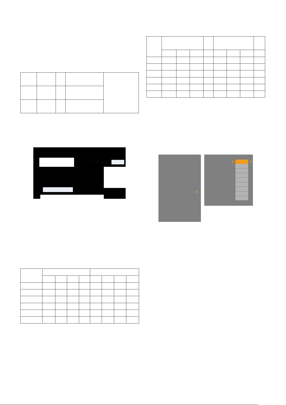
1) Enter ‘EZ ADJUST’ mode by pushing ‘ADJ’ key.
2) Select each ‘Tool Option(1 ~ 5)’ and push ‘OK’ or ‘
G’ key.
3) Correct the number. (Each model has their number.)
4) Correction Tool option is completed.
3.1. ADC Process
* You need not connecting RGB(D-sub) cable. Because ADC
uses TV internal pattern.
• Enter ‘EZ ADJUST’ mode by pushing ‘ADJ’ key,
• Enter ‘ADC Calibration’ mode by pushing ‘OK’ or “G ” key
after selecting “6. ADC Calibration”.
<Caution> Turn on Tv by pushing ‘POWER ON’ or ‘P-ONLY’ key.
* ADC Calibration Protocol (RS232)
Adjust Sequence
• aa 00 00 [Enter Adjust Mode]
• xb 00 40 [Component1 Input (480i)]
• ad 00 10 [Adjust 480i Comp1]
• xb 00 60 [RGB Input (1024*768)]
• ad 00 10 [Adjust 1024*768 RGB]
• aa 00 90 End Adjust mode
* Required equipment : factory Service Remote control
3.2. Function Check
(1) Check display and sound
- Check Input and Signal items.
1) TV
2) AV 1/2
3) COMPONENT1/2 (480i)
4) RGB (PC : 1024 x 768 @ 60hz)
5) HDMI 1/2/3
6) PC Audio In
* Display and Sound check is executed by remote control.
- 9 -
LGE Internal Use OnlyCopyright © 2011 LG Electronics. Inc. All right reserved.
Only for training and service purposes
Item CMD1 CMD2 Data0
Adjust A A 0 0 When transfer the ‘Mode In’,
‘Mode In’ Carry the command.
ADC Adjust A D 1 0 Automatically adjustment
(The use of a internal pattern)
ADC Calibration
ADC Comp 480i
NG
ADC Comp 1080p
NG
ADC RGB
NG
Start Reset
EZ ADJUST
0. Tool Option1
1. Tool Opti on2
2. Tool Option3
3. Tool Option4
4. Tool Option5
5. Country Group
6. ADC Calibration
7. White Balance
8. 10 Point WB
9. Test Pattern
10. EDID D/L
11. Sub B/C
12. V-Com
13. P-Gamma
4. Total Assembly line process
4.1. Adjustment Preparation
· W/B Equipment condition
CA210 : CH 9, Test signal : Inner pattern (85IRE)
· Above 5 minutes H/run in the inner pattern. (Turn on TV by
pushing “POWER ON” or “P-ONLY” key)
* Connecting picture of the measuring instrument
(On Automatic control)
Inside Pattern is used when W/B is controlled. Connect to auto
controller or push Adjustment remote control POWER ON ->
Enter the mode of White-Balance, the pattern will come out.
* Auto-control interface and directions
1) Adjust in the place where the influx of light like floodlight
around is blocked. (illumination is less than 10 lux).
2) Adhere closely the Color Analyzer (CA210) to the module
less than 10cm distance, keep it with the surface of the
Module and Color Analyzer’s Prove vertically.(80° ~ 100°).
3) Aging time
- After aging start, keep the power on (no suspension of
power supply) and heat-run over 15minutes.
- Using ‘no signal’ or ‘full white pattern’ or the others, check
the back light on.
• Auto adjustment Map(RS-232C)
** Caution **
Color Temperature : COOL, Medium, Warm.
One of R Gain/G Gain/ B Gain should be kept on 0xC0, and
adjust other two lower than C0.
(when R/G/B Gain are all C0, it is the FULL Dynamic Range
of Module)
* Manual W/B process using Adjustment remote control
• Enter ‘EZ ADJUST’ mode by pushing “ADJ” key,
• Enter White Balance by pushing “
G
” key at “6.White Balance”.
- After all adjustments, press “IN START” key and compare
Tool option value with its BOM, if it is correctly same then
unplug the AC cable.
If it is not same, then correct it same with BOM and unplug AC
cable.
For correct it to the model’s module from factory JIG model.
- Push ‘IN STOP’ key after completing the function inspection.
4.2. DDC EDID Write (RGB 128Byte )
• Connect D-sub Signal Cable to D-sub Jack.
• Write EDID Data to EEPROM(24C02) by using DDC2B
protocol.
• Check whether written EDID data is correct or not.
* For Service main Assembly, EDID have to be downloaded to
Insert Process in advance.
4.3. DDC EDID Write (HDMI 256Byte)
• Connect HDMI Signal Cable to HDMI Jack.
• Write EDID Data to EEPROM(24C02) by using DDC2B
protocol.
• Check whether written EDID data is correct or not.
* For Service main Assembly, EDID have to be downloaded to
Insert Process in advance.
- 10 -
LGE Internal Use OnlyCopyright © 2011 LG Electronics. Inc. All right reserved.
Only for training and service purposes
Cool 1,100 ºK X=0.276(±0.002)
Y=0.283(±0.002)
Medium 9,300 ºK X=0.285(±0.002)
Y=0.293(±0.002)
Warm 6,500 ºK X=0.313(±0.002)
Y=0.329(±0.002)
Full White Pattern
COLOR
ANALYZER
TYPE: CA-210
RS-232C Communication
CA-210
RS-232C COMMAND MIN CENTER MAX
[CMD ID DATA] (DEFAULT)
Cool Mid Warm Cool Mid Warm
R Gain jg Ja jd 00 172 192 192 192
G Gain jh Jb je 00 172 192 192 192
B Gain ji Jc jf 00 192 192 172 192
R Cut 64 64 64 128
G Cut 64 64 64 128
B Cut 64 64 64 128
Index Equipment -> Wireless unit Wireless unit -> Set
CMD1 CMD2 Set ID Data CMD1 CMD2 CMD3 CMD4
Start w b 0 00 1F 04 00 00
Gain start w b 0 10 1F 04 00 10
Gain End w b 0 1F 1F 04 00 1F
Offset Start w b 0 20 1F 04 00 20
Offset End w b 0 2F 1F 04 00 2F
End w b 0FF1F0400FF
White Balance
Color Temp.
Cool
R-Gain
172
G-Gain
172
B-Gain
192
R-Cut
64
G-Cut
64
B-Cut
64
Test-Pattern
Backlight
ON
100
Reset
To Set
EZ ADJUST
0. Tool Option1
1. Tool Opti on2
2. Tool Option3
3. Tool Option4
4. Tool Option5
5. Country Group
6. ADC Calibration
7. White Balance
8. 10 Point WB
9. Test Pattern
10. EDID D/L
11. Sub B/C
12. V-Com
13. P-Gamma
4.4. EDID DATA
1) All Data : HEXA Value
2) Changeable Data :
*: Serial No : Controlled / Data:01
**: Month : Controlled / Data:00
***: Year : Controlled
****: Check sum
- Auto Download
• Enter ‘EZ ADJUST’ mode by pushing
‘ADJ’ key.
• Enter EDID D/L mode.
• Enter ‘START’ by pushing ‘OK’ key.
* Caution : Never connect HDMI & D-sub
cable when auto download.
* EDID data and Model option download (RS232)
- Manual Download
* Caution
1) Use the proper signal cable for EDID Download
- Analog EDID : Pin3 exists
- Digital EDID : Pin3 exists
2) Never connect HDMI & D-sub Cable at the same time.
3) Use the proper cables below for EDID Writing.
4) Download HDMI1, HDMI2, HDMI3 separately because
each data is different.
(1) RGB EDID data : 128 byte
(2) HDMI EDID data : 256 byte
* Detail EDID Options are below.
ⓐ Product ID
ⓑ Serial No: Controlled on production line.
ⓒ Week, Year:Fixed as S/W released day(same as MES data)
ex) Week : 0x02(2), Year 0x13(2009)
ⓓ Model Name(Hex):
ⓔ Checksum: Changeable by total EDID data.
ⓕ Vendor Specific(HDMI)
MODEL RGB HDMI1 HDMI2 HDMI3 Remark
FHD 0x1C 0xD7, 0x39 0xD7, 0x29
012 3 4 5 67 8 9ABCD EF
00 00 FF FF FF FF FF FF 00 1E 6D ⓐⓑ
10 ⓒ 01 03 68 10 09 78 0A EE 91 A3 54 4C 99 26
20 0F 50 54 A1 08 00 81 80 61 40 45 40 31 40 01 01
30 01 01 01 01 01 01 02 3A 80 18 71 38 2D 40 58 2C
40 45 00 A0 5A 00 00 00 1E 01 1D 00 72 51 D0 1E 20
50 6E 28 55 00 A0 5A 00 00 00 1E 00 00 00 FD 00 3A
60 3E 1E 53 10 00 0A 20 20 20 20 20 20 ⓓ
70 ⓓ 00 ⓔ
LGE Internal Use OnlyCopyright © 2011 LG Electronics. Inc. All right reserved.
Only for training and service purposes
- 11 -
HDMI1 NG
HDMI2 NG
HDMI3 NG
RGB NG
Start Reset
EDID D/L
HDMI1 OK
HDMI2 OK
HDMI3 OK
RGB OK
Start Reset
EDID D/L
EZ ADJUST
0. Tool Option1
1. Tool Option2
2. Tool Option3
3. Tool Option4
4. Tool Option5
5. Country Group
6. ADC Calibration
7. White Balance
8. 10 Point WB
9. Test Pattern
10. EDID D/L
11. Sub B/C
12. V-Com
13. P-Gamma
MODEL HEX EDID Table DDC Fuction
FHD 0001 01 00 Analog/Digital
MODEL Model name(HX)
All Model 00 00 00 FC 00 4C 47 20 54 56 0A 20 20 20 20 20 20 20
INPUT MODEL NAME(HEX) Remark
HDMI1 67 03 0C 00 10 00 B8 2D
HDMI2 67 03 0C 00 20 00 B8 2D
Item CMD1 CMD2 Data0
Download A A 0 0 When transfer the ‘Mode In’,
‘Mode In’ Carry the command.
Download A E 00 10 Automatically Download
(The use of a internal pattern)
D-sub to D-sub DVI-D to HDMI or HDMI to HDMI
For HDMI EDID
For Analog EDID
0123456789 ABCDEF
00 00 FF FF FF FF FF FF 00 1E 6D ⓐⓑ
10 ⓒ 01 03 80 10 09 78 0A CF 74 A3 54 4C 99 26
20 0F 50 54 A1 08 00 81 80 61 40 45 40 31 40 01 01
30 01 01 01 01 01 01 02 3A 80 18 71 38 2D 40 58 2C
40 45 00 A0 5A 00 00 00 1E 01 1D 00 72 51 D0 1E 20
50 6E 28 55 00 A0 5A 00 00 00 1E 00 00 00 FD 00 3A
60 3E 1E 53 10 00 0A 20 20 20 20 20 20 ⓓ
70 ⓓ 01 ⓔ
80 02 03 20 F1 4E 10 1F 84 13 05 14 03 02 12 20 21
90 22 15 01 26 15 07 50 09 57 07 ⓕ
A0 ⓕ E3 05 03 01 01 1D 80 18 71 1C 16 20 58 2C
B0 25 00 A0 5A 00 00 00 9E 01 1D 00 80 51 D0 0C 20
C0 40 80 35 00 A0 5A 00 00 00 1E 02 3A 80 18 71 38
D0 2D 40 58 2C 45 00 A0 5A 00 00 00 1E 66 21 50 B0
E0 51 00 1B 30 40 70 36 00 A0 5A 00 00 00 1E 00 00
F0 00 00 00 00 00 00 00 00 00 00 00 00 00 00 00 ⓔ
Item
Manufacturer ID
Version
Revision
Condition
GSM
Digital : 1
Digital : 3
Data(Hex)
1E6D
01
03

4.5. V-COM Adjust
(Only M+S models which use LGD module)
- Why need Vcom adjustment?
A The Vcom (Common Voltage) is a Reference Voltage of
Liquid Crystal Driving.
-> Liquid Crystal need for Polarity Change with every frame.
- Adjust sequence (Method 1)
· Push ‘PIP’ key.
· If there is no flicker at default value, turn down or turn up
until no flicker, push ‘OK’ key to store.
· Push ‘Exit’ key to exit.
- Adjust sequence (Method 2)
· Enter ‘EZ ADJUST’ mode by pushing “ADJ” key.
· Select and enter ‘12. V-Com’ mode.
· If there is no flicker at default value, turn down or turn up
until no flicker, push ‘OK’ key to store.
· Push ‘Exit’ key to exit.
4.6. Outgoing condition Configuration
- Push ‘IN-STOP’ key, the in-stop processing will start.
If processing i complete, TV will turn off automatically.
(Must not AC power OFF during blinking)
4.7. Internal pressure
Confirm whether is normal or not when between power
board's ac block and GND is impacted on 1.5kV(dc) or
2.2kV(dc) for one second.
- 12 -
LGE Internal Use OnlyCopyright © 2011 LG Electronics. Inc. All right reserved.
Only for training and service purposes
V-Com
V-Com
425
EZ ADJUST
0. Tool Option1
1. Tool Option2
2. Tool Option3
3. Tool Option4
4. Tool Option5
5. Country Group
6. ADC Calibration
7. White Balance
8. 10 Point WB
9. Test Pattern
10. EDID D/L
11. Sub B/C
12. V-Com
13. P-Gamma
Press ( ) to save.
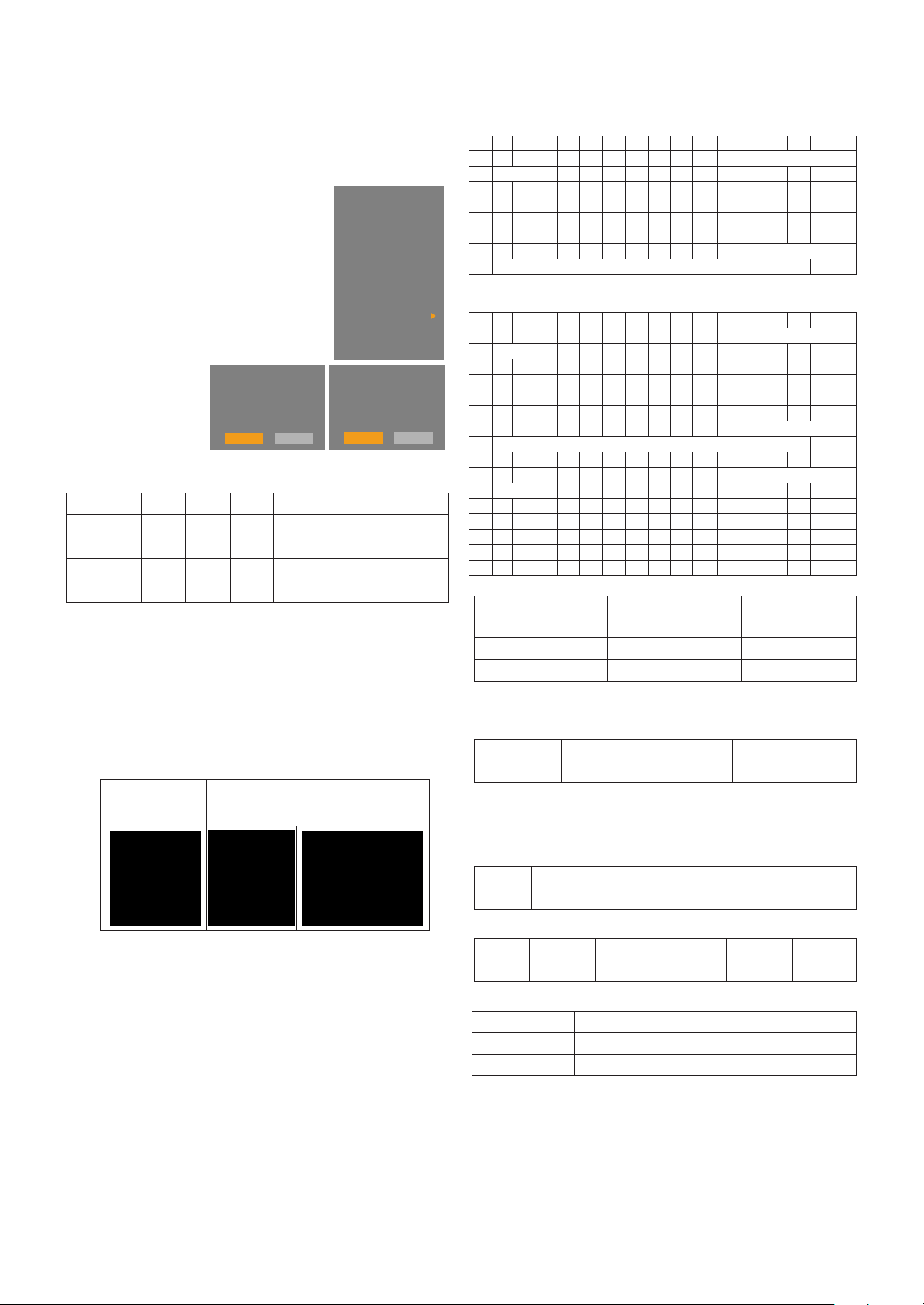
Row Li ne
Column Li ne
CLC
CST
Pane l
S
Y
S
T
E
M
Gat e Driv e IC
So urce D r iv e I C
Circuit Block
Tim i ng
Cont r o ll er
Po w er
Blo c k
V
COM
Gamma
Ref er ence V oltage
Gamm a Re ference
Volta ge
Data (R,G ,B) & C on tro l signal
Cont rol si gnal
Data (R,G,B ) &
Cont rol si gnal
In t er fa ce
TFT
Po w er I np u t
Power Input
Da ta I n pu t
Da ta I n pu t
V
COM
Liquid
Crys tal
V
COM
LGE Internal Use OnlyCopyright © 2011 LG Electronics. Inc. All right reserved.
Only for training and service purposes
- 13 -
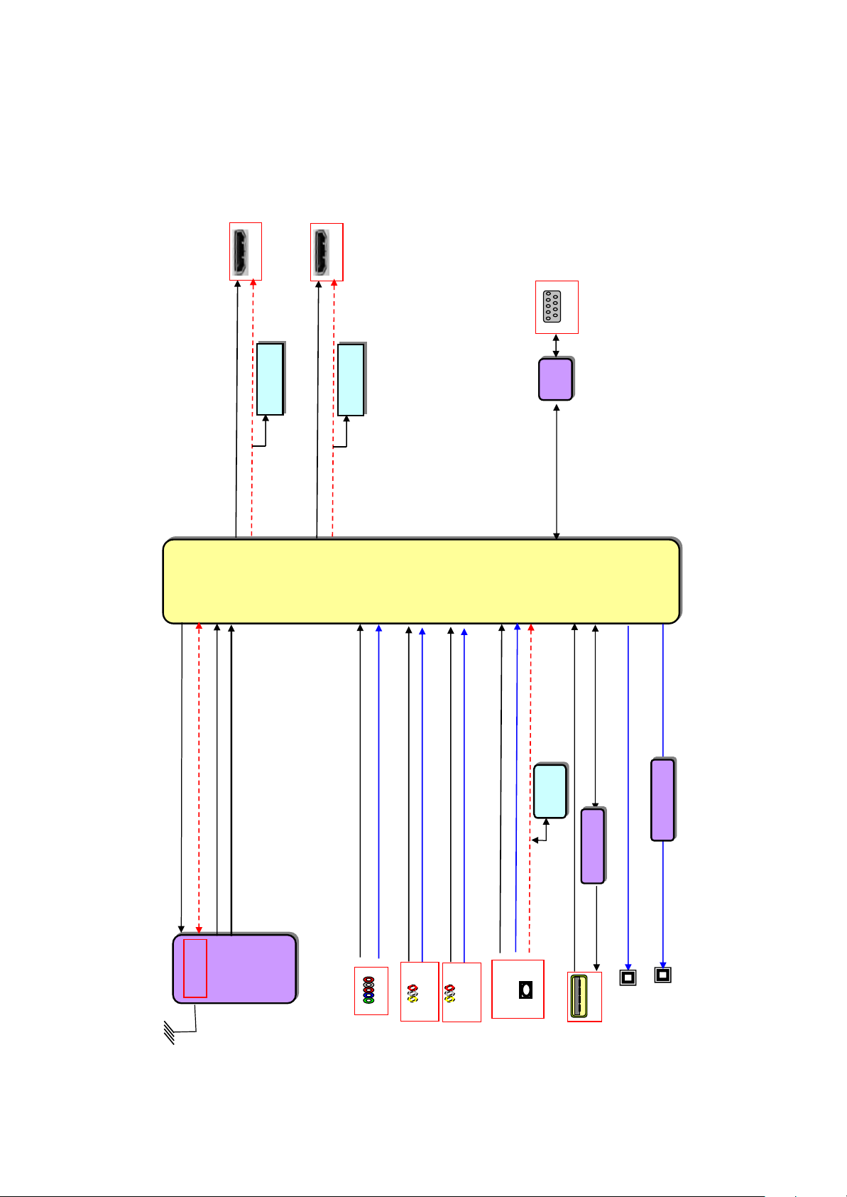
BLOCK DIAGRAM
1. INPUT
Saturn7
MSD301
(IC101)
Saturn7
Saturn7
MSD301
MSD301
(IC10
(IC10
1
1
)
)
Option: S7
S7-Tcon
NIM TUNER
TU3701
(Optio n: TU3702
HNIM tuner )
NIM TUNER
TU3701
(Optio n: TU3702
HNIM tuner )
3 : RF_SWITCH_CTL , FE_BOOSTER_CTL, Tuner Reset
2 : TU_CVBS/SIF (ATV)
Inner Demo d:
LG3911
4 : TU_SCL/SDA , Demod_SCL /SDA
11 : TS_Sync/data[ 0..7]Ö (DTV)
(JK1603)
7:Comp_DE T,Y+/-,Pb+/-,Pr+/-
2: Comp _R/L _IN
JK1604
2:CVBS_DET,CVBS IN
2: CVBS _R/L _IN
EEPROM
(2K, IC400)
EEPROM
(2K, IC400)
(P1104)
(JK1102)
9: R+/ - ,G+/-, B +/-,H /V sync, DET, ISP_RXD/TXD
2: RGB_DDC_SC L/ SDA
2: PC _R/L _IN
(JK1101)
MAX3232
(IC1101)
MAX3232
MAX3232
(IC1101
(IC1101
)
)
2 : SIDE_USB_DM/ DP
1 : 5V _USB
2 : USB_CTL, USB_OCD
MIC2009YM6-TR
(IC2301)
MIC2009YM6
MIC2009YM6
-
-
TR
TR
(IC
(IC
23
23
01)
01)
RGB In
PC Audi o
AV1
COMP1
USB
(Side)
(P2301)
SPDIF (Digital)
JK103
1 : S PDIF_OUT
EXT SPK
2: EXT_OUT_L/R
(JK802)
8:HDMI1_D0+/-,D1+/-,D2+/-,CK+/-
2: DDC_SCL1/SDA1
EEPROM
(2K,IC801)
EEPROM
(2K,IC801)
HDMI1 In
(JK803)
2: DDC_SCL4/SDA4
EEPROM
(2K,IC804)
EEPROM
(2K,IC804)
HDMI4 In
8:HDMI4_D0+/-,D1+/-,D2+/-,CK+/-
2: S7_RXD/TXD
RS232
JK3302
2:SideAV_DET/CVBS IN
2: CVBS _R/L _IN
AV2
(Side)
TPA3124D2PWPR
(IC10)
TPA3124D2PWPR
TPA3124D2PWPR
(IC10)
(IC10)
HP_L/ROUT
 Loading...