

Page 1
SERVICE MANUAL
MA606<Rev.002>20154SERVICE MANUAL
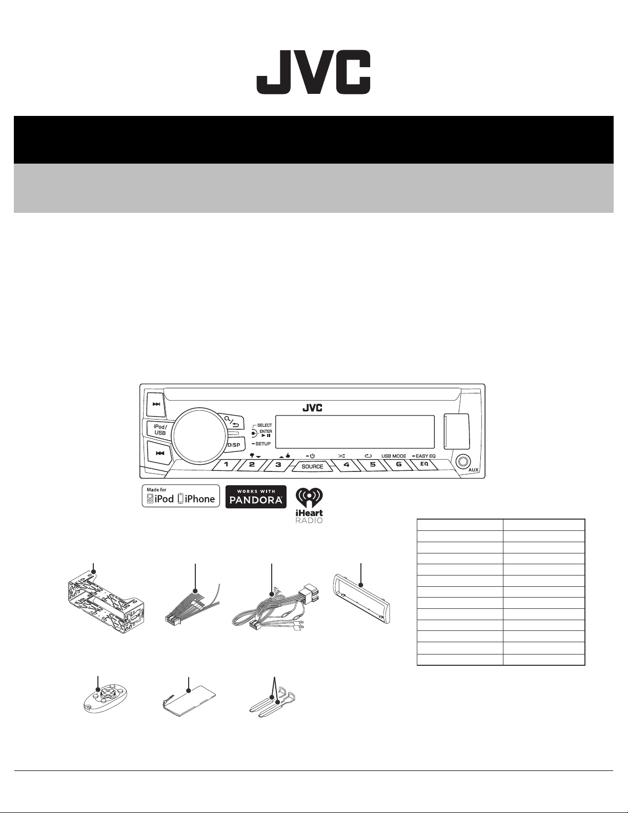
KD-X120EE, KD-X120EU, KD-X120U,
KD-X120UT, KD-X125EE, KD-X220E,
KD-X220EN, KD-X220EY, KD-X220J,
KD-X220U, KD-X220UR, KD-X220UT
DIGITAL MEDIA RECEIVER
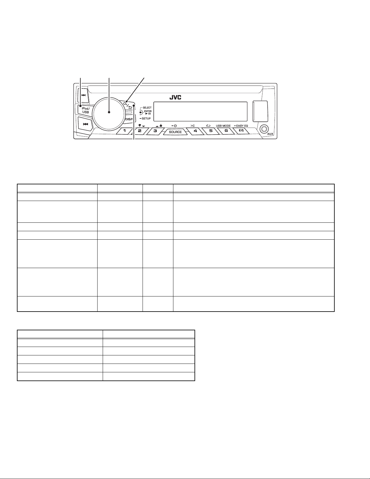
Mounting sleeve
(GE20342-001A)
Remote control unit
(RM-RK52M)
COPYRIGHT © 2015 JVC KENWOOD Corporation
DC cord
(QAM1329-001)
Carrying case
(GE40521-001A)
COPYRIGHT © 2015 JVC KENWOOD Corporation
DC cord
(QAM13xx-00x)
Hook
(GE40646-001A) x2
Lead free solder used in the board (material: Sn-Ag-Cu, melting point: 219 Centigrade)
Lead free solder used in the board (material: Sn-Cu, melting point: 230 Centigrade)
Trim Plate
(GE20363-001A)
DETACHABLE PANEL
Model Parts number
KD-X120EE
KD-X120EU
KD-X120U
KD-X120UT
KD-X125EE
KD-X220E
KD-X220EN
KD-X220EY
KD-X220J
KD-X220U
KD-X220UR
KD-X220UT
CP-X120EED
CP-X120EUD
CP-X120UD
CP-X120UD
CP-X125EED
CP-X220ED
CP-X220ED
CP-X220ED
CP-X220JD
CP-X220UD
CP-X220UD
No.MA606<Rev.002>
2015/4
Page 2
SPECIFICATION
For US
TUNER
FM Frequency Range 87.9 MHz - 107.9 MHz (200 kHz step)
87.5 MHz - 108.0 MHz (50 kHz step)
Channel Space Selection 50 kHz/200 kHz
Usable Sensitivity (S/N = 26 dB) 8.2 dBf (0.71 µV/75 Ω)
Quieting Sensitivity(DIN S/N = 46 dB) 17.2 dBf (2.0 µV/75 Ω)
Frequency Response (±3 dB) 30 Hz - 15 kHz
Signal-to-Noise Ratio (MONO) 64 dB
Stereo Separation (1 kHz) 40 dB
AM Frequency Range 530 kHz - 1 700 kHz (10 kHz step)
531 kHz - 1 611 kHz (9 kHz step)
Channel Space Selection 9 kHz/10 kHz
Usable Sensitivity (S/N = 20 dB) 29 dBµ (28.2 µV)
USB
USB Standard USB 1.1, USB 2.0 (Full speed)
Compatible Devices Mass storage class
File System FAT12/ 16/ 32
Maximum Supply Current DC 5 V 1 A
D/A Converter 24 Bit
Frequency Response (±1 dB) 20 Hz - 20 kHz
Signal-to-Noise Ratio (1 kHz) 105 dB
Dynamic Range 88 dB
Channel Separation 90 dB
MP3 Decode Compliant with MPEG-1/2 Audio Layer-3
WMA Decode Compliant with Windows Media Audio
AAC Decode AAC-LC ".m4a" files
WAV Decode RIFF waveform Audio Format (Linear PCM only)
FLAC Decode FLAC files
Auxiliary
Frequency Response (±3 dB) 20 Hz - 20 kHz
Input Maximum Voltage 1 000 mV
Input Impedance 30 kΩ
Audio
Maximum Output Power 50 W × 4 or 50 W × 2 + 50 W × 1 (Subwoofer = 4 Ω)
Full Bandwidth Power(at less than 1 % THD) 22 W × 4
Speaker Impedance 4 Ω - 8 Ω
Preout Level/Load (USB) 2 500 mV/10 kΩ
Preout Impedance ≤ 600 Ω
General
Operating Voltage (10.5 V - 16 V allowable) 14.4 V
Maximum Current Consumption 10A
Operating Temperature Range 0°C to + 40°C
Installation Size (W × H × D) 182 mm × 53 mm × 108 mm (7-3/16" × 2-1/8" × 4-5/16")
Weight 0.58 kg (1.3 lbs)
• Subject to change without notice.
(No.MA606<Rev.002>)2/20
Page 3
SPECIFICATION
For Europe
TUNER
FM Frequency Range (KD-X220) FM: 87.5 MHz - 108.0 MHz (50 kHz step)
Frequency Range (KD-X125/KD/X120) FM: 87.5 MHz - 108.0 MHz (50 kHz step)
FM-LO: 65.0 MHz - 74.0 MHz (30 kHz step)
Usable Sensitivity (S/N = 26 dB) 0.71 µV/75 Ω
Quieting Sensitivity(DIN S/N = 46 dB) 2.0 µV/75 Ω
Frequency Response (±3 dB) 30 Hz - 15 kHz
Signal-to-Noise Ratio (MONO) 64 dB
Stereo Separation (1 kHz) 40 dB
AM Frequency Range MW 531 kHz - 1 611 kHz (9 kHz step)
LW 153 kHz - 279 kHz (9 kHz step)
Usable Sensitivity (S/N = 20 dB) MW:28.2 µV
SW:50 µV
USB
USB Standard USB 1.1, USB 2.0 (Full speed)
Compatible Devices Mass storage class
File System FAT12/ 16/ 32
Maximum Supply Current DC 5 V 1 A
D/A Converter 24 Bit
Frequency Response (±1 dB) 20 Hz - 20 kHz
Signal-to-Noise Ratio (1 kHz) 105 dB
Dynamic Range 88 dB
Channel Separation 90 dB
MP3 Decode Compliant with MPEG-1/2 Audio Layer-3
WMA Decode Compliant with Windows Media Audio
AAC Decode AAC-LC ".m4a" files
WAV Decode RIFF waveform Audio Format (Linear PCM only)
FLAC Decode FLAC files
Auxiliary
Frequency Response (±3 dB) 20 Hz - 20 kHz
Input Maximum Voltage 1 000 mV
Input Impedance 30 kΩ
Audio
Maximum Output Power 50 W × 4 or 50 W × 2 + 50 W × 1 (Subwoofer = 4 Ω)
Full Bandwidth Power(at less than 1 % THD) 22 W × 4
Speaker Impedance 4 Ω - 8 Ω
Preout Level/Load (USB) 2 500 mV/10 kΩ
Preout Impedance ≤ 600 Ω
General
Operating Voltage (10.5 V - 16 V allowable) 14.4 V
Maximum Current Consumption 10A
Operating Temperature Range 0°C to + 40°C
Installation Size (W × H × D) 182 mm × 53 mm × 108 mm
Weight 0.58 kg
• Subject to change without notice.
(No.MA606<Rev.002>)3/20
Page 4
SPECIFICATION
For ASIA
TUNER
FM Frequency Range 87.5 MHz - 108.0 MHz (50 kHz step)
Usable Sensitivity (S/N = 26 dB) 8.2 dBf (0.71 µV/75 Ω)
Quieting Sensitivity(DIN S/N = 46 dB) 17.2 dBf (2.0 µV/75 Ω)
Frequency Response (±3 dB) 30 Hz - 15 kHz
Signal-to-Noise Ratio (MONO) 64 dB
Stereo Separation (1 kHz) 40 dB
AM Frequency Range Band 1 (MW): 531 kHz - 1 611 kHz (9 kHz step)
Band 2 (SW1): 2 940 kHz - 7 735 kHz (5 kHz step)
Band 3 (SW2): 9 500 kHz - 10 135 kHz /11 580 kHz - 18 135 kHz (5 kHz
step)
Channel Space Selection Band 1: 9 kHz
Band 2/3: 5 kHz
Usable Sensitivity (S/N = 20 dB) MW: 29 dBµ (28.2 µV)
SW: 30 dBµ (32 µV)
USB
USB Standard USB 1.1, USB 2.0 (Full speed)
Compatible Devices Mass storage class
File System FAT12/ 16/ 32
Maximum Supply Current DC 5 V 1 A
D/A Converter 24 Bit
Frequency Response (±1 dB) 20 Hz - 20 kHz
Signal-to-Noise Ratio (1 kHz) 105 dB
Dynamic Range 88 dB
Channel Separation 90 dB
MP3 Decode Compliant with MPEG-1/2 Audio Layer-3
WMA Decode Compliant with Windows Media Audio
AAC Decode AAC-LC ".m4a" files
WAV Decode RIFF waveform Audio Format (Linear PCM only)
FLAC Decode FLAC files
Auxiliary
Frequency Response (±3 dB) 20 Hz - 20 kHz
Input Maximum Voltage 1 000 mV
Input Impedance 30 kΩ
Audio
Maximum Output Power 50 W × 4 or 50 W × 2 + 50 W × 1 (Subwoofer = 4 Ω)
Full Bandwidth Power(at less than 1 % THD) 22 W × 4
Speaker Impedance 4 Ω - 8 Ω
Preout Level/Load (USB) 2 500 mV/10 kΩ
Preout Impedance ≤ 600 Ω
General
Operating Voltage (10.5 V - 16 V allowable) 14.4 V
Maximum Current Consumption 10A
Operating Temperature Range 0°C to + 40°C
Installation Size (W × H × D) 182 mm × 53 mm × 108 mm
Weight 0.58 kg
• Subject to change without notice.
(No.MA606<Rev.002>)4/20
Page 5
SECTION 1
PRECAUTION
1.1 Safety Precautions
(1) This design of this product contains special hardware and
many circuits and components specially for safety purposes. For continued protection, no changes should be made
to the original design unless authorized in writing by the
manufacturer. Replacement parts must be identical to
those used in the original circuits. Services should be performed by qualified personnel only.
(2) Alterations of the design or circuitry of the product should
not be made. Any design alterations of the product should
not be made. Any design alterations or additions will void
the manufacturers warranty and will further relieve the
manufacture of responsibility for personal injury or property
damage resulting therefrom.
(3) Many electrical and mechanical parts in the products have
special safety-related characteristics. These characteristics are often not evident from visual inspection nor can the
protection afforded by them necessarily be obtained by using replacement components rated for higher voltage, wattage, etc. Replacement parts which have these special
safety characteristics are identified in the Parts List of Service Manual. Electrical components having such features
are identified by shading on the schematics and by ( ) on
the Parts List in the Service Manual. The use of a substitute
replacement which does not have the same safety characteristics as the recommended replacement parts shown in
the Parts List of Service Manual may create shock, fire, or
other hazards.
(4) The leads in the products are routed and dressed with ties,
clamps, tubings, barriers and the like to be separated from
live parts, high temperature parts, moving parts and/or
sharp edges for the prevention of electric shock and fire
hazard. When service is required, the original lead routing
and dress should be observed, and it should be confirmed
that they have been returned to normal, after reassembling.
1.2 Warning
(1) This equipment has been designed and manufactured to
meet international safety standards.
(2) It is the legal responsibility of the repairer to ensure that
these safety standards are maintained.
(3) Repairs must be made in accordance with the relevant
safety standards.
(4) It is essential that safety critical components are replaced
by approved parts.
(5) If mains voltage selector is provided, check setting for local
voltage.
1.4 Critical parts for safety
In regard with component parts appearing on the silk-screen
printed side (parts side) of the PWB diagrams, the parts that are
printed over with black such as the resistor ( ), diode ( )
and ICP ( ) or identified by the " " mark nearby are critical
for safety. When replacing them, be sure to use the parts of the
same type and rating as specified by the manufacturer.
(This regulation dose not Except the J and C version)
1.5 Remote control
The Lithium battery is in danger of explosion if replaced incorrectly. Replace it only with the same or equivalent type.
1.6 Preventing static electricity
Electrostatic discharge (ESD), which occurs when static electricity stored in the body, fabric, etc. is discharged, can destroy the
semi conductors. Take care to prevent this when performing repairs.
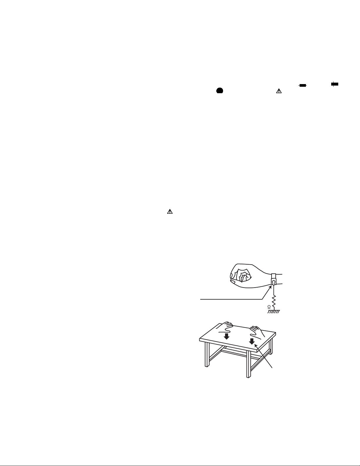
1.6.1 Grounding to prevent damage by static electricity
Static electricity in the work area can destroy the semi conductors.
Be careful to use proper grounding in the area where repairs are
being performed.
(1) Ground the workbench
Ground the workbench by laying conductive material (such
as a conductive sheet) or an iron plate over it before placing the unit on it.
(2) Ground yourself
Use an anti-static wrist strap to release any static electricity
built up in your body.
(caption)
Anti-static wrist strap
1M
Conductive material
(conductive sheet) or iron plate
1.3 Caution
Burrs formed during molding may be left over on some parts
of the chassis.
Therefore, pay attention to such burrs in the case of preforming repair of this system.
(No.MA606<Rev.002>)5/20
Page 6
SECTION 2
SPECIFIC SERVICE INSTRUCTIONS
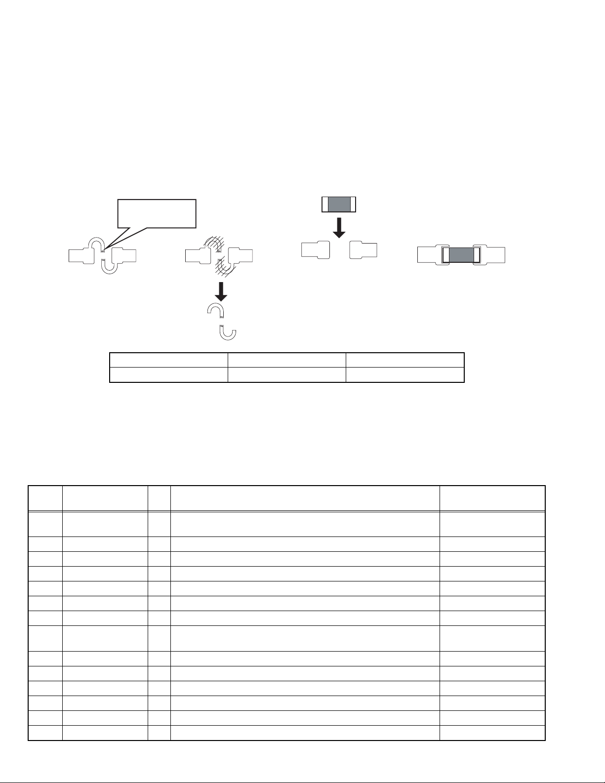
2.1 How to repair a fuse pattern
2.1.1 Purpose of fuse pattern
In order to prevent serious damage on the circuit, fuse pattern is prepared on the GND line of RCA Terminal. This damage may
take due to improper part replacement with a external equipment via RCA line.
2.1.2 Repair Procedure
(1) Check the shorted circuit at the meltdown point.
Need to clean up if the shorted circuit or carbonization happen at the fuse pattern.
(2) Add following part on the fuse pattern.
(3) Check output level.
Meltdown point
Part Number Part Name SPEC
F53-0513-08 PATTERN FUSE 4A
2.1.3 After finished repair
Due to improper part replacement, this meltdown occurs.
Thus please notice following information when the unit is returned to your customer.
Things to be checked before installing the unit.
(1) Check the GND line of external amplifier or other equipment which must connect properly.
(2) Check whether the GND line is not short-circuited with the battery terminal. (do not short-circuit these lines)
2.2 MICROCOMPUTER’S TERMINAL DESCRIPTION
IC701 (R5S726A0D216FP) on MAIN PWB ASSY
Pin No. Pin Name I/O Application
1 LCD_INH O Display On/Off Control L: Display OFF/
2 DAB_COM_ON O Enable DAB micon (For DAB model) H: ON/L: OFF
2 NC O No Use (for non DAB model)
3 PVcc - Power supply for I/O circuits
4 DZF I Zero Input Detect L: Mute OFF/H: Mute ON
5Vss -GND
6 PANEL_PON O Supply Control to Panel L: ON/H: OFF
7 DC_ERR2 I Detect DC Clip (for ST Power Amp IC) L: DC Error ON/
8 PWIC_MUTE O Muting Output for Power Amp IC L: Mute ON/H: Mute OFF
9 LCD_CE O LCD Driver IC Chip Enable Output (for LCD Model)
10 Vss - GND
11 LCD_CLK O LCD CLK Output
12 Vcc - Power supply
13 RGB_CLK O I2C Clock Output for RGB Driver (For RGB Model)
Processing/Operation/
Description
H: Display ON
H: DC Error OFF
(No.MA606<Rev.002>)6/20
Page 7

Pin No. Pin Name I/O Application
13 PCB_TEST_MODE
_RX
14 LCD_DATA_SYS O LCD DATA Output (for LCD Model)
14 LCD/
RGB_DATA_SYS
14 PCB_TEST_MODE
_TX
15 USB_PON O Enable Output for High Side Switch L: HisideSW OFF/
16 PVcc - Power supply for I/O circuits
17 BT_DATA_BT I BT Data Input (For BT model only)
17 NC O No Use (for non BT model)
18 Vss - GND
19 BT_DATA_SYS O BT Data Output (For BT model only)
19 NC O No Use (for non BT model)
20 Vcc - Power supply
21 PWIC_STBY O Output to Power On Power Amp IC L: Standby/H: Play
22 SXM_DATA_SXM I SXM Data Input (For SXM model only)
22 NC O No Use (for non SXM model)
23 SXM_DATA_SYS O SXM Data Output (For SXM model only)
23 NC O No Use (for non SXM model)
24 DEBUG_1A O For Debug
24 DAB_COM_CLK O Clock to DAB (for DAB model only)
24 HD_SPICLK O Clock to HD Decoder (for HD model only)
25 DEBUG_1B O For Debug
25 DAB_REQ_SYS O Command Request from main micon to DAB micon (for DAB model)
25 HD_REQ_SYS O Command Request from SYS-com to HD (for HD model)
26 DEBUG_1C O For Debug
26 DAB_DATA__SYS O DAB Data Output (for DAB model only)
26 HD_DATA_SYS O HD Data Output (for DAB model only)
27 DAB_DATA_DAB I DAB Data Input (for DAB model only)
27 HD_DATA_HD I HD Data Input (for HD model only)
27 NC O No Use (for non DAB / HD model)
28 PVcc - Power supply for I/O circuits
29 FREQ_SEL O Frequency Select Pulse: Power On/
30 Vss - GND
31 ENC2 I Volume Encoder Pulse Input 2
32 ENC1 I Volume Encoder Pulse Input 1
33 REMO I Remocon Input L (Pulse): Remote control
34 LCD_DATA_LCD I LCD DATA Intput (for LCD Model)
35 MRC_DATA_MRC I Marine REMO Data Input UART 57.6kHz (For MARINE model)
35 DEBUG_2A O For Debug
36 PVcc - Power supply for I/O circuits
37 NC O System Clock Output to External Devices (for LCD Model)
I PCB Test Mode RX
O LCD and RGB DATA Output (for RGB Model)
O PCB Test Mode TX
No Use
Processing/Operation/
Description
H: HisideSW ON
L: Power Off
data/H: Standby
(No.MA606<Rev.002>)7/20
Page 8

Pin No. Pin Name I/O Application
38 Vss - GND
39 RESET I Reset Input
40 Vss - GND
41 PLLVcc - Power supply for PLL
42 PAN_DET I Panel Detection input L: Panel Attached/
43 Vcc - Power supply
44 EXTAL I High Speed Clock 12MHz
45 XTAL O High Speed Clock 12MHz
46 Vss - GND
47 Vss - GND
48 PVcc - Power supply for I/O circuits
49 D-0 I/O USB Data- 0
50 D+0 I/O USB Data+ 0
51 ASEMD I ASE Mode Select Pin
52 NC I No Use
53 BT_MUTE I BT Mute L: Mute OFF/H: Mute ON
53 NC I No Use (for non BT model)
54 STAGE2 I Model Selecting Input 2
54 STEERING_REMO2I OE Remote In 2 (for DOP models)
Processing/Operation/
Description
H: Panel Detached
55 STAGE1 I Model Selecting Input 1
55 STEERING_REMO1I OE Remote In 1 (for DOP models)
56 TEL_MUTE I Tel Mute Detection Input (for JVC Model)
56 LINE_MUTE I Line Mute Detection Input (For KWD Model)
56 No Use I No Use (for non support Tel mute model)
57 DC_ERR1 I Detect DC Offset Error from EVOL IC L: DC Error ON/
H: DC Error OFF
58 Avss - GND
59 Avcc - Power Supply
60 Avref - Reference Power Supply
61 TRST I Debugging Interface. Reset Input.
62 ASEBRKAK/ASE-
BRK
63 TDO O Debugging Interface. Serial Output for Instructions and Data
64 TDI I Debugging Interface. Serial Input for Instructions and Data
65 TMS I Debugging Interface. Test Mode Select Signal Input.
66 TCK I Debugging Interface. Test Clock Input.
67 AUDIO_X2 O Audio Clock 16.9MHz (for External DAC)
68 AUDIO_X1 I Audio Clock 16.9MHz (for External DAC)
69 PVcc - Power supply for I/O circuits
70 SPBCLK O FLASH SPI Multi I/O Bus Clock output
71 Vss - GND
72 SPBSSL O FLASH SPI Multi I/O Bus Slave Select Output
73 SPBIO0 I/O FLASH SPI Multi I/O Bus I/O Data 0
74 SPBIO1 I/O FLASH SPI Multi I/O Bus I/O Data 1
I/O Emulator Break Mode Acknoledge/Break Input
(No.MA606<Rev.002>)8/20
Page 9

Pin No. Pin Name I/O Application
75 SPBIO2 I/O FLASH SPI Multi I/O Bus I/O Data 2
76 Vss - GND
77 SPBIO3 I/O FLASH SPI Multi I/O Bus I/O Data 3
78 Vcc - Power supply
79 MD_CLK I Clock Mode Set (Power ON Reset)
EXTAL Pin Input Clock Ranges from 10 to 12 MHz
80 MD_BOOT I BOOT Mode Set L: Boot mode 0/
81 AUDIO_XOUT O DAC Audio Clock Output 16.9MHz
82 PVcc - Power supply for I/O circuits
83 DAB_PON O Control 3..3V power for DAB Module (for DAB model only) H: ON/L: OFF
83 HD_PON O Control 3.3V power for HD module (for HD model only) HD source= H: ON/
83 NC O No Use (for non DAB/non HD model)
84 Vss - GND
85 MUTE O Muting Output for Evol & Line Out L: Mute ON/H: Mute OFF
86 Vcc - Power supply
87 BT_RST O BT Reset Output (For BT model) L: Reset ON/
87 NC O No Use (for non BT model)
88 DCDC6V_PON O Enable Output for DC-DC Regulator
89 SXM_PWR O Power Supply for SXM (For SXM model only) L: PWR Off/H: PWR On
89 NC O No Use (for non SXM model)
90 DAB_REQ_DAB I Command Request from DAB micon to main micon
90 NC O No Use (for non DAB model)
91 EVOL_SCL I/O I2C Clock 391kHz for E-Vol
91 EP_SCL I/O I2C Clock 391kHz for E2PROM
91 TU_SCL I/O I2C Clock 391kHz for Tuner
92 EVOL_SDA I/O I2C Data for E-Vol
92 EP_SDA I/O I2C Data for E2PROM
92 TU_SDA I/O I2C Data for Tuner
93 IPOD_SCL O iPod Authentication IC I2C Clock Clock speed 23kHz
93 NC O No Use (For non-iPod Model)
94 IPOD_SDA O iPod Authentication IC I2C Data
94 NC O No Use (For non-iPod Model)
95 REG_SCL O I2C Clock for Regulator IC
96 REG_SDA O I2C Data for Regulator IC
97 NC O No Use
98 DIM_IN I Dimmer Control Input (for JVC Model) L: Dimmer Detect ON/
98 NC O No Use (For KWD Model) keep L output setting
99 REG_FLG I Power Detection L: Detect OFF/
100 Vss - GND
101 PVcc - Power supply for I/O circuits
102 MRC_REQ_MRC I Command Request from Marine REMO to SYS-com
(For MARINE model)
Processing/Operation/
Description
H: Boot mode 1
Other source= L: OFF
H: Reset OFF
H: Dimmer Detect OFF
H: Detect ON
(No.MA606<Rev.002>)9/20
Page 10
Pin No. Pin Name I/O Application
102 NC O No Use (for non Marine model)
103 SSISCK O DAC Audio Serial Data Clock 44.1kHz
104 SSIWS1 O DAC L/R Clock 44.1kHz
105 MRC_PON O Enable Marine REMO Power Supply (For MARINE model)
105 DEBUG 2C O For Debug H: Power On / L: Power Off
106 SSITx O Servo DSP Data Output
107 Vss - GND
108 DAC_CCLK O DAC Control Data Clock
109 Vcc - Power supply
110 DAC_CDTI O DAC control Data Input
111 TU_RST O HELIO/CAYMAN (HD) Reset L: Reset ON/
111 NC O No Use (For non DAB/HD model)
112 PVcc - Power supply for I/O circuits
113 MRC_DATA_SYS O Marine REMO Data Output UART 57.6kHz (For MARINE model)
113 NC O No Use (for non Marine model)
114 Vss - GND
115 DAC_CS O DAC Chip Select
116 BEEP O Output for Beep Tone Generator H (Pulse): BEEP/L: OFF
117 MRC_REQ_SYS O Command Request from SYS-com to Marine REMO
(For MARINE model)
117 NC O No Use (for non Marine model)
118 PCB_TEST_MODE I PCB Test Mode Switch L: Normal Mode/H: Check
118 WDT O Watch Dog Timer output L: Normal Mode /
119 MRC_EN O Marine REMO Data Select (For MARINE model)
119 DEBUG_2B O For Debug
119 Field Test 2 O RDS data log output (standby for field test)
120 Field Test 1 O RDS data log output (standby for field test)
120 FDAC_RST O DAC reset L: DAC reset/
Processing/Operation/
Description
H: Reset OFF
Mode (After Reset software need to check the
pin input. If detect high it
should enter Serial Number mode)
H: Reset by WDT
H: DAC reset off
(No.MA606<Rev.002>)10/20
Page 11
SECTION 3
DISASSEMBLY
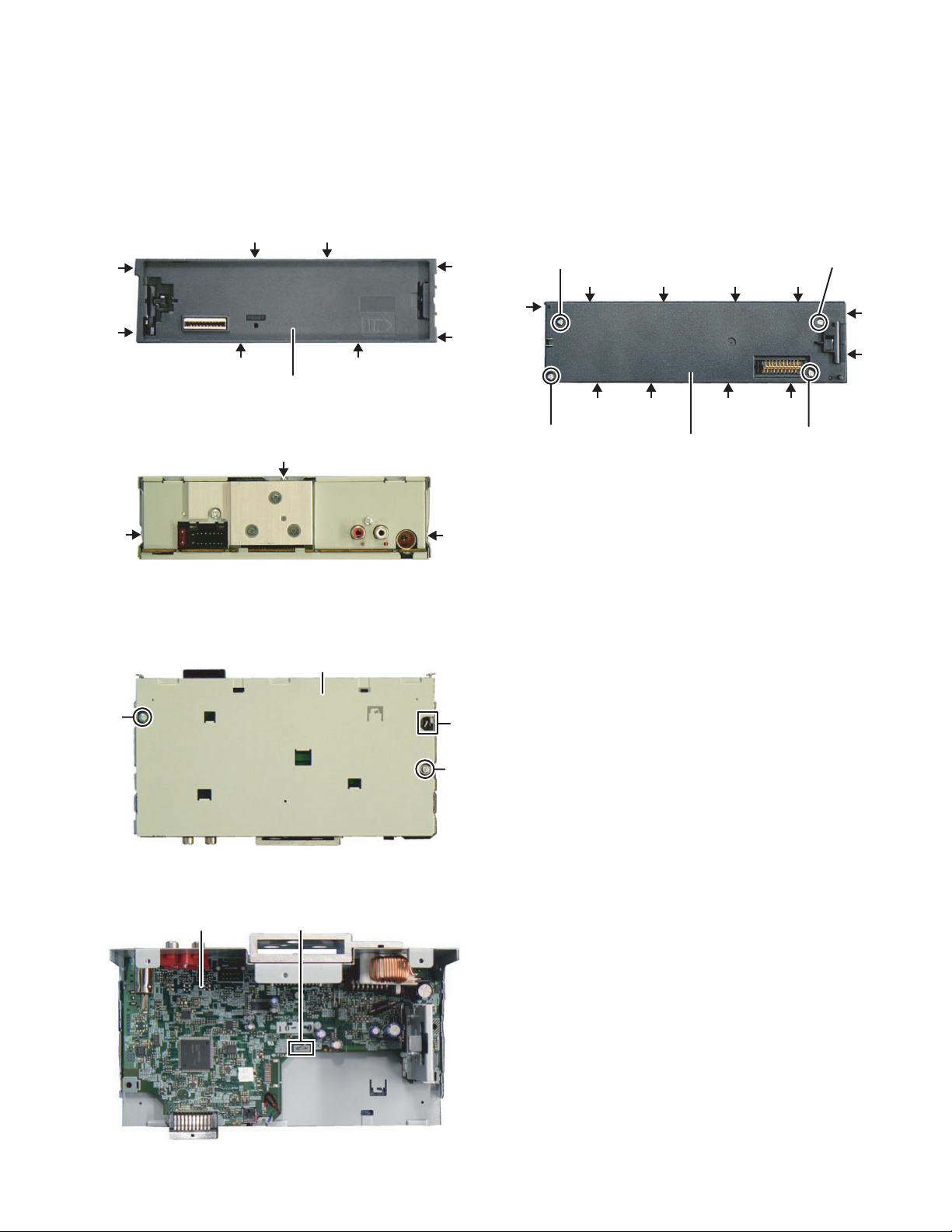
3.1 Main body
3.1.1 Removing the MAIN PWB (See Fig.1 to 4)
(1) Disengage the 8 hooks a, and remove the FRONT CHAS-
SIS ASSY.
(See Fig.
1)
aa
a
a
aa
FRONT CHASSIS ASSY
Fig.1
(2)
Remove the 3 screws A . (See Fig.
2)
A
A
Fig.2
(3) Remove the 2 screws B. (See Fig.3)
(4) Disengage the 1 hook b, and remove the BOTTOM
COVER with MAIN PWB.
(See Fig.3)
BOTTOM COVER
A
3.1.2 Removing the SWITCH PWB (See Fig.5)
(1) Remove the VOLUME KNOB.
(2) Remove the 4 screws D.
(3) Disengage the 11 hooks d, and remove the REAR
COVER.
(4) Remove the SWITCH PWB.
a
D
d d d d
d
D
d
a
d
d ddd
D
REAR COVER
Fig.5
D
B
Fig.3
(5) Disengage the 1 hook c, and remove the MAIN PWB.
(See Fig.4)
MAIN PWB
c
Fig.4
b
B
(No.MA606<Rev.002>)11/20
Page 12
SECTION 4
ADJUSTMENT
4.1 Outline
4.1.1 Panel
ACCENT SEARCHVOL
RETURN
A symbol "" in the key column indicates that the key should be pressed and held for 1 second or longer.
4.1.2 Test Modes
These test modes are available in normal production ROM.
Transition to Test Mode shall be available during DC Error detection.
Test Mode Mode Source Operation
Production Test Mode - All Press and hold [DISP] key and [SOURCE] key and reset.
Service Test Mode Normal Mode /
Production Mode
Service Information Clear Mode - All Press and hold [RETURN] key and [SOURCE] key and reset.
DC Error Information Mode - All Press and hold [DISP] key and [] key and reset.
DOP Test Mode Normal Mode All Pressing and holding [SELECT] key, press [DISP] key for 7 sec-
Bluetooth Device Name Select
Mode
Tunisia Area /
Tuner Span Change Mode
4.1.3 Release from Test Mode
These actions will release the Test Mode and transit back to Normal Mode
Method Remarks
Reset All Modes
Momentarily voltage drop All Modes
ACC OFF All Modes
POWER OFF All Modes
Panel Detach All Modes
Normal Mode BT Audio Pressing and holding [ACCENT] key, press [DISP] key for 3 sec-
Normal Mode All Pressing and holding [VOL] key, press [RETURN] key for 3 sec-
All Pressing and holding [DISP] key, press [] key for 7 seconds.
(Starting to press [DISP] key and [] key at the same time can not
be entered into the mode)
onds.
(Starting to press [SELECT] key and [DISP] key at the same time
can not be entered into the mode)
onds.
(Starting to press [ACCENT] key and [DISP] key at the same time
can not be entered into the mode)
onds.
(No.MA606<Rev.002>)12/20
Page 13
4.2 Production Test Mode
Press and hold [1] key and [3] key and reset.
4.2.1 Test Mode Defaults
During Production Test Mode, the following settings defer from the Normal Mode.
The settings will change immediately after mode activation.
Difference in action Setting value
Period to prohibit TEL/LINE MUTE function (Normal Mode: 10 secs) 1 second
Writing-in to E2PROM when DC error is detected Prohibited
"DEMO" item in Setup Menu OFF
Power supply during ACC OFF (Back Up On) MUTE terminal turns OFF after 2 seconds
"BEEP" item in Setup Menu ON
Volume range 0 to 44
Source change interval timer 0 seconds
When detected the 0 bit mute Mute off
Various setting item Setting value
Default Volume 15
"BASS BOOST" OFF
"LOUDNESS" OFF
"TEL MUTING" ON
Initial Source FM (Mechaless Models) /
CD (Non-Mechaless Models)
Language English
EQ FLAT
Fader / Balance Center
Digital Track Expander / Sound Reconstruction Set OFF
"VOL ADJUST" / "VOLUME OFFSET" 0
DEMO Mode Setting OFF
4.2.2 Mode structure
The following table shows the test modes that can be accessed from the different sources in Production Test Mode.
Source Test mode
Tuner TUNER Test Mode
USB USB Test Mode
4.2.3 Mode content
Syscon shall display the following information after entering Production Test Mode.
Display content Details
All lights on (BOTH LCD & LED including dual color switchable)
Set should not be able to power on if sub clock is not functioning.
The display is released when another operation is executed.
4.2.4 Special Operation by Key Input
Behaviour Details
Volume Adjustment to 44
Only during Normal display
(Invalid during Menu)
4.2.5 How to transit to Version Display Mode
Item Operation Display content Details
Transit to Display
Mode
RETURN
Pressing and holding [DISP] key, press [] key for 0.5 seconds.
(Starting to press [DISP] key and [] key at the same time can not be entered into
the mode)
Transit to Version Display Mode
(Default status: All Lights ON)
(No.MA606<Rev.002>)13/20
Page 14
4.2.6 Version Display Mode
Item Operation Display content Details
All Lights ON/
All lights ON
TEST
Syscom version
display
Stage Setting ##: Stage Setting for current hardware
Y–SS##@@@
TSAGE :21 ##
## = File Number
@@@ = Syscon Version Number
Serial No. Display (8 digits)
Serial No. display
SN 00000000
Display to support ASCII characters
********: Blank
@@@@@@@@: EEPROM Read Error
DISP
(Toggle)
## = Blank: Verifying
OK: IC mounted
NG: IC not mounted
iPod IC Mount
Verification Status
Display
(USB models
only)
iPod ##
**: Non iPod support model
In addition, upon entering this mode, P-CON is
turned ON.
When a result is OK, P-CON is turned off.
Upon exit, P-CON remains OFF.
When a result is NG, P-CON is kept ON condition.
Upon exit, P-CON remains ON.
Pre-out Switch
(1 Pre-out / 2 Pre-
EQ
L/O SU B.W
Switch Pre-out with toggle
out model only)
Mode release
SOURCE
Transition
Mode release RETURN
Return to Normal mode
Return to Normal mode
4.2.7 Tuner Test Mode Specification
The following display shall be indicated according to the TUNER status.
Status Display content Details
TUNER IC
Communication Error
RDS/RBDS Specified
data reception
TUN CON NG
DRS STTE
Communication to TUNER IC not available
(indicated unless the mode is in Clock Display Mode).
Turn OFF P-CON forcibly if PS=RDS TEST is received.
P-CON recovers with Power OFF/ON.
Item Operation Display content Details
Display TUNER IC version
TUNER IC display EQ
TA2********
'AT2 ********' is eg "AtomIC2 57V1B101" indicating
"AtomIC2 TEF6657V1B 1.01"
*Not applicable and no function for HD and DAB models
(No.MA606<Rev.002>)14/20
Page 15

4.2.8 USB Test Mode Specification
Applicable for iPod model only.
Status Display content Details
## = Blank: Verifying
NG: IC not mounted
**: Non iPod support model
Upon source change to USB source or USB
device plug in:
Verifying: Show "iPod: ##"
NG: Always show "iPod: NG" even during "NO
DEVICE" or playback.
**: Always show "iPod: **" even during "NO
iPod IC Mount Verification Status
Display
iPod ##
DEVICE"
OK: Change back to nomal display ("NO DE-
VICE / normal playback display).
In addition, upon enter to this mode, P-CON is
turned ON.
When a judgment result is OK, P-CON is
turned off.
Upon exit, P-CON still remain OFF.
When a judgment result is NG, P-CON is kept
ON condition.
Upon exit, P-CON still remain ON.
4.3 Service Test Mode
In the STANDBY source, while pressing and holding [2] key, press [6] key for 7 seconds.
(Starting to press [2] key and [6] key at the same time can not be entered into the mode)
4.3.1 Default status immediately after the mode activation
It shall be same as the normal activation.
4.3.2 Mode content
Syscon shall display the following information after entering this mode.
Display content Details
RSVT TES
Display is released when an operation is executed.
4.3.3 Common operation mode for only STANDBY sources
Item Operation Display content Details
Syscom version
display
6
Y–SS##@@@
## = File Number
@@@ = Syscon Version Number
00 to 50 are displayed in "XX".
Power ON
duration display
OPNTM HX0X
2
OPNTM XXXXX
For less than 1 hour, the display is indicated per 10
minutes.
00001 to 10922 are displayed in "XXXXX".
MAX 10922 (hours)
(No.MA606<Rev.002>)15/20
Page 16
4.4 Service Information Clear Mode
Press and hold [2] key and [5] key and reset.
4.4.1 Default status immediately after the mode activation
It shall be same as normal activation.
4.4.2 Mode content
After entering this mode, Syscon shall clear the information stored for service and output the result to the display.
Cleared information changes will take place only after reset.
Display Display content Details
Data Clear in
IIINTALIZE
Data Clearing in Progress.
Progress
Data Clear OK Data cleared successfully.
Data Clear NG Data cleared with error, clear the data.
TDA A CLR OK
TDA A CLR NG
Display Blinks (250ms interval)
The following table shows the data that is cleared.
Information to Clear Details Storage area
Service information
DC error information
CD EJECT number of times display E2PROM
Forced Power OFF information display E2PROM
DC error 1 display (wrong connection & other detection information in detecting duration) E2PROM
DC error 2 display (capacitor leakage detection number information) E2PROM
Tuner Area Setting E2PROM
Tuner information
Preset Frequency E2PROM
Preset PI code E2PROM
Tagging information Token data memory index E2PROM
4.5 DC Error Information Mode
Press and hold [3] key and [6] key and reset.
4.5.1 Default status immediately after the mode activation
It shall be same as normal activation.
4.5.2 Mode content
Syscon shall display the following information after entering this mode.
Display content Details
DC ERR
DC OK
When DC error is detected
When DC error is not detected
Item Operation Display content Details
DC 1 ER R
DC ERR1display
DC1 OK
When wrong connection & DC error in other detection duration is detected.
When wrong connection & DC error in other detection duration is not detected.
Clear detection information when wrong connection
DC ERR1 clear
DC1 OK
& DC error in other detection duration is displayed.
(Clear data flash)
Display detecting number of times in capacitor leak-
DC ERR2 display
DC2 4
age detection duration.
#: 0 to 4
Clear number of times for detection information in
DC ERR2 clear
DC 2 0
capacitor leakage detection duration. (Clear data
flash)
(No.MA606<Rev.002>)16/20
Page 17
4.6 DOP Test Mode
Pressing and holding [SELECT] key, press [DISP] key for 7 seconds.
4.6.1 DOP Mode Common Setting
Common settings for all car makers are as follows:
Demo: No demo animation
Remove all DEMO related items
Power on animation: Show carmaker's name
Only opening animation will show "Car maker's name"
Setup menu: Delete Demo
Color setting for RGB model: Refer to manufacturer preference below:
4.6.2 EEPROM DOP Read Error Display
In the case of an EEPROM read error or EEPROM DOP read error, the unit will behave accordingly.
(1) No Power on animation
(2) No Demo animation
(3) Demo removed in setup menu
(4) Color settings set to default
(5) Serial number display replaced by "SN @@@@@@@@"
4.6.3 Mode content
1) Enter DOP Mode. Pressing and holding [SELECT] key, press [DISP] key for 7 seconds.
Display content Details
PMODEDO
2) Select manufacturer setting.
Note: RGB color save as USER color. DEFAULT color set to USER.
The order is priority. Lower Priority brand need to press and hold(2 secs)
: press and hold (2 second) on button mentioned as follow
Display content Operation Display content Color
No Demo 1
Toyota 2
Honda 3
Ford 4
Suzuki 5
Hyundai 6
Mitsubishi
FIAT
Iveco DISP
Alfa Romeo 1
KIA 2
Volkswagen 3
Chevrolet 4
Peugeot 5
Nissan 6
Isuzu
Skoda
Daihatsu DISP
Default RETURN
JVC
TOYOTA
HONDA
FORD
SUZUKI
HYUNDA I
MI TSUBISHI
FIAT
IVECO
ALFA ROMEO
KIA
VOL KSWAGEN
CHE VRO L E T
PEUGEOT
NISSAN
ISUZU
SKODA
DAIHATSU
DEFAUL T
(same as Daihatsu)
Blue
Lime
Blue
Greenish Blue
Yellow Amber
Blue
Apple
White
White
Red
Blue
White
Red
Green
Orange
Red
Yellowish Green
Yellow Amber
(Same as Suzuki)
Return to default JVC normal setting.
7
25
5
3
16
7
14
User
User
13
7
User
13
24
16
13
User (R=22, G=31, B=0)
15
(No.MA606<Rev.002>)17/20
Page 18
4.7 Tuner Span Change Mode
Pressing and holding [VOL] key, press [RETURN] key for 3 seconds.
4.7.1 Default status immediately after the mode activation
It shall be same as normal activation.
After selection of the setting item, the receiver should exit this mode and return to the display before entering this mode.
This setting will be stored in EEPROM.
4.7.2 Mode content
Syscon shall display the following information after entering this mode.
Item Operation Display content Details
Tuner Span
Change Mode
VOL +/-
(*1)
Tuner Span
Change Mode
VOL +/-
(*2)
Release Mode VOL
ARE A AS I A
AREA TUNISIA
AREA EUROPE
AREA TUNISIA
Default setting for Asia models.
Change to 'Asia' area type.
Change to 'Tunisia' area type.
Default setting for Europe models.
Change to 'Europe' area type.
Change to 'Tunisia' area type.
Depending on display pattern in normal mode.
*1: Only applicable for Asia ('U') models
*2: Only applicable for Europe ('E') models
(No.MA606<Rev.002>)18/20
Page 19
4.8 DC Offset error description
A
4.8.1 DC Offset detection circuit design
• Purpose:
To prevent breakdown, when occur DC offset between speaker output "+" and "-".
• Target:
Detect DC offset, then stop the Power Amp operation and shift
to specified condition.
4.8.2 Possible causes of DC offset at speaker output lines
(1) Mis-connection for Speaker output for example touch to car
body or battery line.
(2) Current leak of coupling capacitor for Power IC input.
(3) Current leak of AC-GND capacitor for Power IC AC-GND.
(4) Capacitor shorted of above parts due to foreign object.
C-tc
E-Vol
Win_TC
Win_In
DC Error
C-in
C-in
R3
C-in
C-in
C-ac2C-ac1
Sw5V
R2
R1
C3
R4
Audio Pwr Amp
In 1
In 2
In 3
In 4
AcGnd
Offset Detect
Out
Micon
ADC In
4.8.5 Manipulate after detect DC Offset
• If detected error 10 consecutive times, and 10th error occurred
in "Mis-connect detection period", judge as "Mis-connect".
• If detected error 10 consecutive times, and 10th error occurred
in "Capacitor leak detection period", judge as "Capacitor leak ".
• If detected error 10 consecutive times, and 10th error occurred
in "Other detection period" and detected another 10 errors consecutively, then judge as "Other".
• If judge as "Mis-connect".
- turn off speaker output.
- display "MISWIRING", check wiring connection then reset.
- key access disable except button of Eject, Reset and service
mode
- record error in EEPROM "DC1 ERR"
- the product is able to be recovered by Reset button.
• If judge as "Capacitor leak ".
- turn off speaker output.
- display "WIRING", check wiring connection then reset.
- key access disable except button of Eject, Reset and service
mode
- record error in EEPROM "DC2 #" (# means counter number)
- the product can be recovered by pressing the Reset button
before the capacitor leak error counter reach "DC2 4".
After that, only clear the counter back to "0" can recover the
product.
• If judge as "Other" (manipulation same as mis-connect)
SECTION 5
TROUBLESHOOTING
4.8.3 Type of checking
4.8.3.1 To detect DC Offset Error
• Mis-connection
- Short any one speaker out line to GND or Vcc
• Capacitor leak
- Parallel 330kΩ to either any one of coupling cap or AC-GND
capacitor (to simulate current leakage of capacitor)
- Shorted either any one of coupling capacitor or AC-GND capacitor.
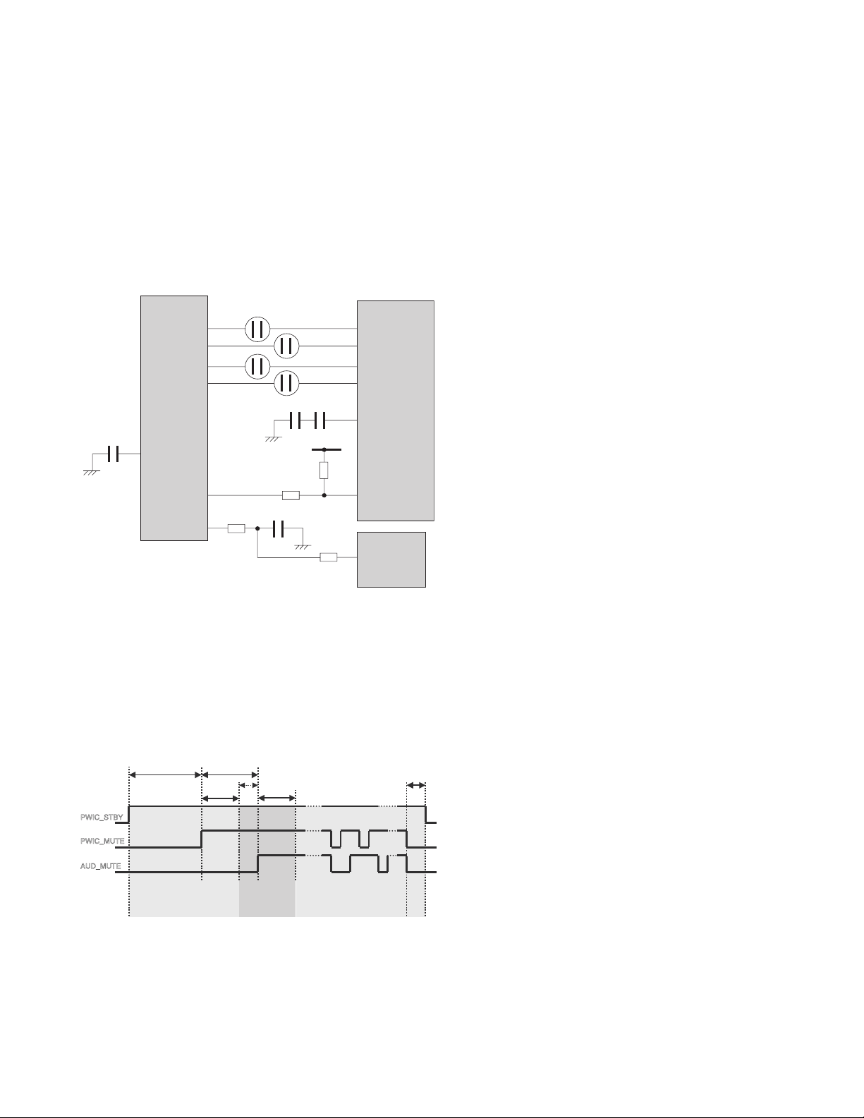
4.8.4 Detection Timing chart
PWIC_STBY
PWIC_MUTE
UD_MUTE
2.0sec or more
Missconnect
detection period
1.5sec or more
0.8sec
0.7sec or more
1.0sec
Capacitor leak
detection period
Other (miss detection etc.)
detection period
50ms
or more
5.1 How to cancel DC offset error
Check to be sure the terminals of the speaker leads are covered
with insulating tape properly, then reset the product.
If an error message does not disappear even after a reset, there
is a need for internal repair.
5.2 How to clear DC offset error recorded in EEPROM
Refer to “4.5 DC Error Information Mode”.
(No.MA606<Rev.002>)19/20
Page 20

JVC KENWOOD Corporation
CE Segment 2967-3, Ishikawa-machi, Hachioji-shi, Tokyo, 192-8525, Japan
(No.MA606<Rev.002>)
Printed in Japan
VSE
Page 21

SCHEMATIC DIAGRAMS
22
DIGITAL MEDIA RECEIVER
KD-X120EE KD-X120EU KD-X120U
KD-X120UT KD-X125EE KD-X220E
KD-X220EN KD-X220EY KD-X220J
KD-X220U KD-X220UR KD-X220UT
(No.MA606<Rev.002>)1/
Page 22

■ PRECAUTIONS ON SCHEMATIC DIAGRAMS
z Due to the improvement in performance, some part numbers shown in the circuit diagrams
may not agree with those indicated in the Parts List.
z The parts numbers, values and rated voltage etc. in the Schematic Diagrams are for
reference only.
z Since the circuit diagrams are standard ones, the circuits and circuit constants may be
subject to change for improvement without any notice.
■ PRECAUTIONS ON PARTS LIST
z
The parts identified by the symbol are critical for safety. Whenever replacing these parts, be sure to
use specified ones to secure the safety.
z
The parts not indicated in this Parts List and those which are filled with lines --- in the Parts No.
columns will not be supplied.
z
P.W. BOARD Ass'y will not be supplied, but those which are filled with the Parts No. in the Parts No.
columns will be supplied.
z
When ordering chips, screws etc., place bulk orders (unit of tens) whenever possible to improve
shipping efficiency.
z
There are cases where the actual implemented parts in the sets and the service parts are different.
When ordering parts, make sure to refer to the Parts List.
■
PRECAUTIONS ON SERVICE
Certain parts of the power circuits and the GNDs differ according to the models. Care must be
taken for the following points as the differences are indicated separately in the LIVE GND ( ) and
the ISOLATED (NEUTRAL) GND ( ).
1. Do not touch the LIVE GND, or do not touch the LIVE GND and the ISOLATED (NEUTRAL)
GND at the same time. It may cause an electric shock.
Before pulling out the chassis or other parts, make sure to pull out the power cord from the
wall outlet first.
2. Do not short circuit between the LIVE GND and ISOLATED (NEUTRAL) GND, or never
measure the LIVE GND and ISOLATED (NEUTRAL) GND at the same time using measuring
instruments (oscilloscope, etc.). It may blow fuses or damage other parts.
■ DEVIATION TOLERANCE RANGE
DEVIATION TOLERANCE RANGE
F G J K M N R H Z P
± 1% ± 2% ± 5% ±10% ±20% ±30%
+30%
-10%
+50%
-10%
+80%
-20%
+100%
-0%
22
(No.MA606<Rev.002>)2/
Page 23

Q931
SW_3.3V
Q471Q470
1
6
RGULATOR
2
IC901
HSW
IC891
DC-DC
8
IC861
EEPROM
IC841
RESET
IC831
FLASH
IC821
MICON
PVCC
IC701
TUNER
IC601
DAC
IC555
IC481
Transceiver
RS-485
IC480
iPod
IC441
POWER_AMP
IC301
EVOL
IC161
REMOCON
IC90
(3 Zone only)
RGB Driver IC
IC2
LCD Driver
IC1
PANEL CONNECTOR
CN701
PANEL CONNECTOR
CN1
BLOCK DIAGRAM-1 (SIGNAL BLOCK)
AUX
USB
J80
J60
KEY MATRIX
F_AUXG
F_AUXR
F_AUXL
D-0
D+0
F_AUXG
F_AUXR
F_AUXL
D-0
D+0
KS6
KS3
KS2
KS1
KI5
KI4
KI3
KI2
KI1
LCD
ED1
COM4
COM3
COM2
COM1
S1 TO S51
P3
P2
P1
P4
P3
P2
P1
RGB
LCD_RGB_DATA_OUT
LCD_DATA_OUT /
RGB_CLK
KS1
KI4
LCD_DATA_IN
LCD_RGB_DATA_OUT
LCD_DATA_OUT /
LCD_INH
LCD_CE
LCD_CLK
ENC2
ENC1
REMO
ENCODER
Single Color
LED
RGB LEDs
EN1
SWR
for MRN_REQ_M)
(Use IRQ or FR6 pin
BT MODULE
For SXI
For MARINE CONTROL
MIC+
MIC-
MRC_EN_SYS
MRC_REQ_SYS
AOUT_L
AOUT_R
RESET
TX
RX
DCERR2
MRC_DA_MRC
MRC_DA_SYS
MRC_REQ_MRC
MRC_PON
FREQ_SEL
DZF
DAC_CDTI
DAC_CLK
DAC_CS
DAC_RST
DAC_LRCK
DAC_SDTI
DAC_BCK
DAC_MCK
LINE_MUTE
RESET
FLAG_REG
PWIC_MUTE
PWIC_STBY
BEEP
MUTE
MUTE
OE_REMOTE
REMOTE
OE
REMOTE
ANT
OFFSET
DC_ERR1
ENC2
PAN_DET
ENC1
REMO
LCD_CE
LCD_CLK
LCD_DATIN
LCD_DATOUT
PON_PANEL
M_DA_SXM
SXM_DA_M
REMO
TEL_MUTE
DIM_IN
BEEP
PWIC_STBY
PWIC_MUTE
RESET
PON_MRN
M_REQ_MRN
MRN_REQ_M
M_EN_MRN
M_DA_MRN
MRN_DA_M
SCL_EV_EP_TU
SDA_EV_EP_TU
SDA_IPOD
SCL_IPOD
SPBSSL
SPBCLK
SPBIO3
SPBIO2
SPBIO1
SPBIO0
E-MUTE
SWL
RROUT/SWR
FROUT
RLOUT/SWL
FLOUT
RROUT
FROUT
RLOUT
FLOUT
SXM_PWR
TEL_MUTE
DIM
MUTE
LINE_MUTE
E_MUTE
SXM_PWR
SXM_TXD
SXM_RXD
SXI
J470
TU_R
TU_L
USB_L
USB_R
SXI_G
SXI_R
SXI_L
&
CONTROL
MOSFET
MUTE
TEL_MUTE
DIMMER
RESET
Mute_Circuit
JACK
ANT
J600
J321
SW
PANEL3.3V
AUX_G
AUX_L
AUX_R
D-0
D+0
PON_USB
CTL
TU3.3V
SCL_EV
SDA_EV
SCL_EET
SDA_EET
SDA_REG
SCL_REG
FLAG_REG
RR-
RR+
RL-
RL+
FR-
FR+
FL-
FL+
GND
DC_P.CORD
CN990
EXT
ACC
ANT
BT_DA_SYS
BT_DA_BT
BT_DA_BT
BT_DA_SYS
BT_R
BT_L
DCERR2
SXM_PWR
MIC
created date:2015-04-22No.MA606
22
(No.MA606<Rev.002>)3/
Page 24

Q931
SW_3.3V
SW
PANEL3.3V
Q701
Q471
Q470
0.35A
11
0.45A
15
0.25A
4
1.3A
5
0.3A
3
13
7
8
1
6
REGULATOR
2
IC901
HSW
IC891
1
DC-DC
8
IC861
1.25V_LDO
IC851
EEPROM
IC841
RESET
IC831
FLASH
IC821
PLLVCC
VCC
MICON
PVCC
IC701
TUNER
IC601
DAC
IC555
IC481
Transceiver
RS-485
IC480
iPod
IC411
POWER_AMP
IC301
EVOL
IC161
REMOCON
IC90
(3 Zone only)
RGB Driver IC
IC2
LCD Driver
IC1
SWITCH PWB
MAIN PWB
BLOCK DIAGRAM-2 (SUPPLY BLOCK)
USB_5V
USB_5V
LCD
ED1
5V
PANEL_3.3V
ILM_10.5V
AUX
USB
J80
J60
RESET
SWITCH
(2 DIN)
KEY MATRIX
Regulator
5V
ILM_10.5V
PANEL_3.3V
ENCODER
Single Color LED
RGB LED
EN1
AND
Gate
SW
3.3V
BT MODULE
For SXI
For MARINE CONTROL
MIC-
2
VCC
8
DGND
DGND
7
MIC+
1
AGND
AGND
6
TEL_MUTE
DIMMER
Mute_Circuit
JACK
ANT
J600 J321
PANEL CONNECTOR
PANEL CONNECTOR
CN1
CN701
VDD
VCC
3.3V
VDDA_RF
VDDA_IFADC
VDDD
BU3.3V
9
SXI
J470
GND2
GND2
TU3.3V
AU9/12V
CD5V
5.2V
ILM10.5V
GND
V6IN
DC_P.CORD
CN990
VCC2
VCC1
EXT
ACC
ANT
VCC
&
CONTROL
MOSFET
AU9
MIC
-
+
created date:2015-04-22No.MA606
22
(No.MA606<Rev.002>)4/
Page 25

AM MODE
ALL RESISTORS ARE 1/10W 5% METAL GLAZE RESISTOR.
ALL CAPACITORS ARE 50V OR 25V CERAMIC CAPACITOR.
1. VOLTAGES ARE DC-MEASURED WITH A DIGITAL VOLT METER WITHOUT INPUT SIGNAL
3. COMPONENTS REFERENCE WITH "?" INDICATE NOT USE.
2. UNLESS OTHERWISE SPECIFIED.
ALL RESISTANCE VALUES ARE IN OHM.
NOTES
CONDITION---FM MODE. ( )USB MODE.
3.3V
0V
0V
0V
3.3V
3.3V
1.5V
1.5V
1.5V
0V
0V
0V
1.5V
1.5V
2.9V
0V
3.3V
3.3V
NO USE
NO USE
(0.1V)
(3.0V)
0V
0V
3.3V
0V
0V
3.3V
3.3V
(1.7V)
0V
(3.1V)
(4.9V)
0V
0V
1.0V
0.9V
2.5V
1.5V
1.2V
1.5V
1.2V
1.5V
1.2V
0V
0V
3.3V
0V
(1.7V)
(3.3V)
0V
(1.7V)
3.3V
0V
0V
3.3V
0V
3.0V
5.0V
2.5V
2.5V
0V
(1.7V)
2.5V
0V
0V
(1.7V)
5.0V
0V
(3.3V)
(1.7V)
3.3V
3.3V
3.3V
0V
0V
0V
14.0V
0V
10.5V
8.5V
5.0V
6.0V
3.3V
3.3V
5.1V
3.3V
3.3V
3.3V
0V
14.3V
14.0V
14.1V
0V
5.1V
0.8V
4.8V
1.6V
9.6V
3.3V
0V
0V
3.3V
3.3V
3.3V
0V
3.3V 3.3V
3.3V
3.3V
3.3V
NO USE
3.3V
3.3V
3.3V
MAIN PWB:J7J-0022-**
3.0V0V
0V
1.5V
3.3V
0V0V0V
0V
0V
0V
0V
0V
3.3V
0V
3.3V
3.3V
0V
0V0V0V
0V
2.8V
1.5V
0V
3.3V
3.3V
3.3V
3.3V
LTA024EEB-X
22K
22K
LTC024EEB-X
47K
10K LTA014YEB-X
4.7K
LTC043TEB-X
22K
22K
0V
3.3V
(ATS10A)
FZB10BT-100
F901
FUSE 10A
0V
0V
1.25V
0V
0V
0V
0V
0V
3.3V
0V
0V
3.3V
0V
3.3V
0V
1.25V0V3.3V0V3.3V0V1.25V
0V
0V
3.3V0V3.3V
3.3V
3.3V0V0V
0V
3.3V
0.1V
0V
3.3V
3.3V
3.3V
0V
1.25V
0V
1.25V
1.9V
1.9V
0V
0V
3.3V
0V
0V
3.3V
0V
0V
*
*
1.5V
3.3V
0V
3.3V
3.3V
1.6V
0V
3.3V
3.3V
3.3V
3.2V
0V0V0V
1.25V
0V
3.3V
3.3V
0V
0V
1.25V
2.0V
0V
0.2V
3.3V
3.2V
0V
0V
3.3V
3.3V
0V
0V
0V
0V
0V
3.3V
1.25V
0V
3.3V
0V
3.3V
3.3V
3.3V
3.3V
3.3V
0V
3.3V
5.1V
5.1V
3.3V
3.3V
3.3V
3.3V
3.3V
3.3V
3.3V
3.3V
3.3V
3.3V
3.3V
3.3V
0V
4.0V
4.0V
4.0V
4.0V
4.0V
4.0V
4.0V
8.4V
3.3V
3.0V
3.0V
3.3V
3.3V
0V
3.2V
0V
7.1V
3.6V
7.1V
14.4V
7.1V
0V
7.1V
7.0V
6.9V
6.9V
6.9V
0V
6.9V
7.1V
7.1V
0V
7.1V
14.4V
7.1V
3.2V
7.1V0V3.2V
0V
0V
3.3V
3.0V
3.0V
0V
0V
0V
0V
DEBUGGING
BT_DATA_BT
DC_ERR1
LCD_DATA_SYS
SXI_AL
EET_SDA
EET_SCL
BT_DATA_SYS
BT_RST
BT.L
BT.R
RESET
TU.R
FREQ_SEL
SXM_DATA_SXM
ENC2
ENC1
FLOUT
DIM_IN
SXM_PWR
MUTE
MIC_N
MIC_P
TU.L
FR+
FL-
TEL_MUTE
DIM_IN
REG_FLG
BT_RST
LCD_DATA_LCD
PAN_DET
REMO
D-
ENC1
D+
ENC2
LCD_CLK
LCD_CE
P3.3V
SXI_AG
AUX-R
AUX-G
AUX-L
SXI_AR
MIC_N
SXI_AR
SXI_AL
SXM_DATA_SYS
DZF
SPBIO0
SPBCLK
SPBIO3
SPBSSL
SPBIO1
SPBIO2
IPOD_SDA
IPOD_SCL
FR-
RESET
FL+
RL+
FR+
RL-
RR-
RR+
FL-
REMO
REG_FLG
REG_SCL
TEL_MUTE
RESET
USB_PON
D-
REMO
RR-
MIC_P
REG_SCL
EET_SDA
EET_SCL
LCD_INH
SXM_PWR
REG_SDA
BT.R
RL+
RL-
FR-
RR+
FL+
DAC_CS
DAC_CDTI
DAC_CLK
DAC_LRCK
DAC_SDTI
DAC_BCK
DAC_MCK
AUX-G
AUX-R
BT.L
LCD_DATA_LCD
BT_DATA_BT
BT_DATA_SYS
RLOUT
RROUT
FROUT
LCD_INH
PANEL_PON
DAC_MCK
DAC_SDTI
DAC_LRCK
USB.R
USB.L
DZF
DAC_CDTI
DAC_CLK
DAC_CS
DAC_RST
PANEL_PON
DAC_RST
REG_FLG
RR/SUBR
RL/SUBL
RROUT
RLOUT
FROUT
MUTE
USB_PON
LCD_DATA_SYS
REG_SDA
DAC_BCK
DC_ERR1
OFFSET
FLOUT
USB.R
PWIC_STBY
EET_SCL
EET_SDA
E_MUTE
FREQ_SEL
BEEP
SXM_DATA_SXM
DC_ERR2
SXM_DATA_SYS
PAN_DET
PWIC_MUTE
SPBCLK
LCD_CE
LCD_CLK
D+
IPOD_SCL
SPBSSL
IPOD_SDA
SPBIO0
SPBIO1
SPBIO2
SPBIO3
RL/SUBL
EET_SDA
SXI_AG
USB.L
AUX-L
OFFSET
EET_SCL
RR/SUBR
FLOUT
E_MUTE
RLOUT
TU.R
FROUT
RROUT
E_MUTE
TU.L
PWIC_MUTE
DC_ERR2
PWIC_STBY
BEEP
GND3
GND2
GND5
GND1
GND4
!
!
!
sure to use the specified one.
When replacing those parts make
Parts are safety assurance parts.!
!
!
!
!
!
!
!
16.9344MHz
NAX1224-001X
X540
12MHz
NAX1243-001X
X701
9.216MHz
L7J-0014-00
X600
F0K-0014-00
VA600
V
?VA601
DAC5
TL03
IP1
TL46
DIST
TL45
AR
TL53
CLD/GND
LCDDAO
LCLK
CE
USBG
AL
TL52
AG
P33
TL07
GND
LDI
V10.5
D-
INH
5V
TL15
VOL2
REM2
D+
PDET
TL18
VOL1
FMIN
TU.L
TL51
TU.R
TL50
SXI.L
TL56
S10
S6
S2
R
L
G
SXI.R
TL57
AC
TL44
RL
FR
FL
SUBR
SUBL
RR
TMUTE
SDA
SCL
DIMMER_IN
TU33
TL09
VCC2
ANT
TL10
ACC
ILM
TL02
EXT
TL11
V61
TL14
AUD
TL04
FLG
TL17
VDD
TL05
VCC1
GND2
MEM
TL01
BUP
REM
TL20
OE
TL21
A.ANT
TL19
RTS2
TL28
RTS1
TL27
DB2A
DB1C
DB1B
DB1A
V1.25
TL06
DAC.R
TL55
DAC.L
TL54
RXM
TL42
TXM
TL41
DB2B
TM
TL43
IP3
TL48
IP2
TL47
IP4
TL49
TDO
TL33
TRST
TL37
TDI
TL34
ASEMD
TL38
ASEBRK
TL39
TMS
TL35
TCK
TL36
CS
TL31
GND2
TL25
ERR1
HOLD
TL26
CLK
TL22
GND1
TL24
VDD
TL32
WP
TL29
DO
TL23
DI
TL30
SW33
TL08
HSSIN
TL12
BT_TX
MICN
BT_RX
A9V
BT_RST
BT_R
AGND
BT_L
DGND
VDD5V
MICP
43
2 1
QSW0648-001Z
S830
1.6k
R701
1/4W
0
R816
2.2k
R302
22k
R273
330
R271
4.7k
R702
12k
R757
20k
R759
1.6k
R705
47k
R1003
?R1002
?R1001
?R1000
?R706
?R477
?R478
2.2k
R715
?R232
?R231
2.2k
R713
100
R611
16k
R700
33k
R1069
2.2k
R710
15k
R729
15k
R727
47k
R723
47k
R721
1.6k
R703
1.6k
R704
1.6k
R707
270
R841
270
R840
47k
R749
100
R755
100
R781
0
R304
100
R754
100
R753
100
R776
100
R777
100
R778
100
R779
4.7k
R766
6.8k
R747
6.8k
R746
4.7k
R765
100
*R410
100
*R411
4.7k
*R412
4.7k
*R413
4.7k
*R414
2.2k
R745
47k
R743
47k
R744
1M
R720
47k
R739
47k
R741
47k
R742
47k
R740
?R373
22k
R360
68k
R370
47k
R730
10k
R372
22
R726
22
R728
2.2k
R725
1M
R724
*R403
?R891
1/4W
4.7k
R390
?R866
100
R760
1.6kR719
1k
R400
0
R431
0
R432
?R230
1/4W
47k
R978
?R243
1k
R714
1k
R712
1/4W
6.8k
R979
_0.5%
10
R1051
100k
R270
?R1052
?R476
1/4W
270
R1004
0
R1082
?R223
1/4W
6.8k
R980
?R470
100
R601
1k
R600
?R227
82
R602
?R226
1/4W
270
R1005
1/4W
270
R1006
?R233
?R225
1/4W
0
R1434
1M
R603
4.7
R605
?R164
?R162
?R228
1M
R604
?R606
?R607
?R609
?R608
?R610
?R13
100
R830
47k
R822
20
R861
39k
R864
0
R612
*R733
*R734
*R732
*R735
1/4W
0
R1076
10
R1404
100k
R717
33k
R361
0
R1429
?R401
22k
R362
4.7k
R364
0
R1419
2.2k
R716
180
R260
?R482
?R221
4.7k
R363
?R1079
0
R1091
0
R1170
?R380
?R222
180
R250
10k
R930
_0.5%
39k
R867
_0.5%
18k
R868
100
R756
?R320
?R340
?R483
1/4W
0
R1061
?R330
?R350
22k
R261
22k
R251
?R321
?R341
1/4W
0
R1428
?R331
220
R574
180
R573
220
R572
91
R571
62
R758
160
R752
200
R751
200
R750
0
R1073
1k
R1070
?R351
330
R262
1/4W
0
*R381
_0.5%
68k
R865
?R253
?R224
330
R252
?R229
1/4W
0
R1075
?R343
?R353
?R1055
?R471
?R239
10k
R171
?R240
?R323
?R333
?R970
?R932
?R931
47k
R821
_0.5%
20k
R890
3.3k
R819
47k
R105
47k
R104
1k
R588
1k
R598
0
R869
0
R589
0
R599
?R179
?R178
100
R168
100
R169
0
R167
1/4W
0
R170
?R402
100k
R365
1/4W
270
R862
?R475
?R474
910
R722
?R473
?R472
?R1022
0
R1060
0
R1071
1/4W
5.1
R303
?R1072
0
R307
470
R100
2.2k
R711
12k
R371
1/4W
47k
R820
1/4W
2.2k
R892
1/4W
47k
R969
0
R103
0
R102
0
R101
?R1090
LTC043TEB-X
Q260
LTC043TEB-X
Q250
?Q471
?Q340
?Q330
?Q350
?Q320
LTA024EEB-X
Q273
LTA014YEB-X
Q701
LTA024EEB-X
Q270
LTC024EEB-X
Q272
?Q930
?Q470
LSCR523UBFS8
Q360
?Q220
LSAR523UBFS8
Q271
?Q931
PFUSE1
?L608
QQR1927-001
L990
10u
L860
4.7u
L591
4.7u
L600
4.7u
L861
?L223
?L220
4.7u
L609
4.7u
L850
0.12u
L606
0.22u
L605
4.7u
L601
0.47u
L602
1.0u
L604
0.1u
L603
0.15u
L607
?L221
NQR0715-001X
L610
NQR0713-001X
L758
NQR0713-001X
L709
NQR0713-001XL822
NQR0713-001XL823
NQR0713-001XL820
NQR0713-001X
L824
NQR0713-001XL821
LB73G0BK-006
L827
*L825
*L826
LB73G0BK-006
L701
NQR0715-001X
L611
?L780
?L222
2221
F_AUXL
20
F_AUXG
19
F_AUXR
18
GND
17
Panel_3.3V
16
ILM10.5
15
LCD/RGB_DATOUT
14
LCD_CE
13
LCD_DATIN
12
RGB_CLK/USB_GND
11
LCD_CLK
10
USB_GND
9
ENC2
8
D+
7
ENC1
6
D-
5
LCD_INH/USB5V
4
USB5V
3
REMO
2
PAN_DET
1
CN701
QGZ2006J1-20
18 17
MEMORY
16
ILUMINATION
15
TEL/NAVI MUTE
14
OE REMOTE
13
REAR RIGHT (+)
12
REAR RIGHT (-)
11
REAR LEFT (-)
10
REAR LEFT (+)
9
FRONT LEFT (+)
8
FRONT LEFT (-)
7
FRONT RIGHT (-)
6
FRONT RIGHT (+)
5NC4
REMOTE/P-CON
3
ACC
2
GND
1
QNZ0607-001
CN990
1211
T10
10T99T88
T7
7T66T55T44
T3
3T22T11
?J470
T8
SUB-L
T7
FRONT-L
T6
(REAR-L)
T5 T4
SUB-R
T3
FRONT-R
T2
(REAR-R)
T1
/REAR-R
/REAR-L
QNN0874-001
J321
321
?J220
DAC_RST/FIELD TEST 1120
MRC_DATA_EN/DEBUG_2B/FIELD TEST 2119
PCB_TEST_MODE118
MRC_REQ_SYS117
BEEP116
DAC_CS115
Vss114
MRC_DATA_SYS113
PVcc112
TU_RST111
DAC_CDTI110
Vcc109
DAC_CCLK108
Vss107
SSITX106
MRC_PON105
SSIWS1104
SSISCK103
MRC_REQ_MRC102
PVcc101
Vss100
REG_FLG99
DIM_IN98
NC97
REG_SDA96
REG_SCL95
IPOD_SDA94
IPOD_SCL93
EV_EP_TU_SDA92
EV_EP_TU_SCL91
NC
90
SXM_PWR
89
DCDC6V_PON
88
BT_RST
87
Vcc
86
MUTE
85
Vss
84NC83
PVcc
82
AUDIO_XOUT
81
MD_BOOT
80
MD_CLK
79
Vcc
78
SPBIO3
77
Vss
76
SPBIO275SPBIO174SPBIO0
73
SPBSSL
72
Vss
71
SPBCLK
70
PVcc
69
AUDIO_X168AUDIO_X2
67
TCK
66
TMS
65
TD164TD0
63
ASEBRKAK/ASEBRK
62
TRST
61
AVref 60
AVcc 59
AVss 58
DC_ERR1 57
TEL_MUTE/LINE_MUTE 56
Stage1/STR_REMO1 55
Stage2/STR_REMO2 54
BT_MUTE 53
NC 52
ASEMD 51
D+O 50
D-O 49
PVcc 48
Vss 47
Vss 46
XTAL 45
EXTAL 44
Vcc 43
PAN_DET 42
PLLVcc 41
Vss 40
RESET 39
Vss 38
NC 37
PVcc 36
MRC_DATA_MRC/DEBUG_2A 35
LCD_DATA_LCD 34
REMO 33
ENC1 32
ENC2 31
Vss30FREQ_SEL29PVcc28NC27DEBUG_1C26DEBUG_1B25DEBUG_1A24SXM_DATA_SYS
23
SXM_DATA_SXM
22
PWIC_STBY21Vcc20BT_DATA_SYS
19
Vss18BT DATA_BT17PVcc16USB_PON15LCD_DATA_SYS/PCB_TEST_MODE_TX
14
PCB_TEST_MODE_RX13Vcc12LCD_CLK11Vss10LCD_CE9PWIC_MUTE8DC_ERR27PANEL_PON6Vss5DZF4PVcc3NC2LCD_INH
1
R5S726A0D216FP
IC701
GND
33
XTAL_IN 32
VSS 31
DAC_L 30
SDA
24
VSSD_IO
23
I2S_SD_016
DR_I_DATA15
DAC_R 29
GPIO_0 28
GPIO_1 27
GPIO_2 26
SCL 25
VDDD
22
VSSD
21
I.C.
20
I2S_SD_1
19
I2S_BCK
18
I2S_WS
17
DR_Q_DATA14
DR_BCK13
DR_WS12
DR_BL11
AM_LNA_CAP10
AM_IN_P9
VSSA_RF
8
VDDA_RF
7
FM_IN_P
6
FM_IN_M
5
FM_CAP
4
VBGP
3
VSSA_IFADC
2
VDDA_IFADC
1
TEF6657HN-X
IC601
SE1R1SE1L2SE2R3SE2L4SE3R5SE3L6QD1R7QD1G8QD1L9QD2R10QD2G11QD2G12QD2L13CREF
14
GND
15
OUTSWL
16
OUTSWR
17
OUTLF
18
OUTLR
19
OUTRR
20
OUTRF
21
WINTC
22
MUTE
23
VCC
24
SCL
25
SDA
26
DCERR
27
WININ
28
TDA7718C_9
IC161
TAB1
1
OFFDET
2
PWGND1
3
OUT2-
4
STBY
5
OUT2+
6
VCC1
7
OUT1-
8
PWGND2
9
OUT1+
10
SVR
11
IN1
12
IN2
13
SGND
14
IN4
15
IN3
16
ACGND
17
OUT3+
18
PWGND3
19
OUT3-
20
VCC2
21
OUT4+
22
MUTE
23
OUT4-
24
PWGND4
25
CD
26
TAB2
27
JCV8034
IC301
MCLK
1
BICK
2
SDTI
3
LRCK
4
RSTN
5
CSN
6
CCLK
7
CDTI
8
NC
9
AOUTR
10
AOUTL
11
VCOM
12
VSS
13
AVDD
14
DVDD
15
DZF
16
AK4387ET
IC555
FLG
14
EXT
1
ANT
2
ILM
3
AUDIO
4
CD
5
ACCIN
6
VCC2
7
VCC1
8
GND
9
SCL
10
VDD
11
SDA
12
V6IN
13
SW33V
15
LV5685PV-H
IC901
9
VCC
8
RST
7
SCL
6
NC5
5
NC4
4
NC3
3
SDA
2
GND
1
MFI337S3959-X
*IC411
PG
1
IN
2
SW
3
GND
4
BST
5
EN/SYNC
6
VCC
7
FB
8
MP9942GJ
IC861
CS
1
DO[IO1]
2
WP[IO2]
3
GND
4
DI[IO0]
5
CLK
6
HOLD[IO3]
7
VCC
8
W25Q16DVSSIG-X
IC821
A0
1
A1
2
A2
3
GND
4
SDA
5
SCL
6
WP
7
VCC
8
BR24T02FJ-W-X
IC841
OUT
6
ILIM
5
FLAG
4
EN
3
GND
2
IN
1
NCP380HSNAJAA-X
IC891
VOUT
5
NC
4
STBY
3
GND
2
VIN
1
BU1CTD3WG-W
IC851
VOUT
4
CT
3
VDD
2
GND
1
BU4228F-W
IC831
EEPROM
HSS_USB
RESET
LDO_1.25V
FLASH
(NO USE)
REAR_MIC
E'VOLUME
(NO USE)
FRONT_PREOUT
(NO USE)
REAR_PREOUT
ANT_CONT
EXT_REMO
SWITCHABLE
REAR/SUB_PREOUT
SW3.3V
DC_DC_CONVERTER
TEL/NAVI_MUTE
AUTO_DIMMER
(NO USE)
BT_MODULE
*POWER_CORD
(NO USE)
SIRIUS/XM/SXI
IPOD_CP_CIRCUIT
PREOUT/P.IC_MUTE
24BIT_DAC
TUNER
BAW56-TP-X
D270
BAW56-TP-X
D271
BAW56-TP-X
D370
?D472
?D1060
?D474
?D475
RSB6.8SM-X
D100
RSB6.8SM-X
D101
?D473
?D1061
?D471
?D222
?D470
DZ2J068M
D360
?D1402
?D1401
?D224
?D223
DZ2J051M
D401
1N5401-BPC04
D990
DB22306
D861
DA2J101
D273
?D381
RB521SM-30-X
D400
?D601
SK34A-L-X
D902
SK34A-L-X
D903
?D602
?D272
?D380
MBRX130
D390
MBRX130
D391
T1111
T1010
T99
T88
T77
T66
T55
T44
T33
T22
T11
?CN228
QEZ0982-476Z
16V
47u
C304
CD04ET1C102M
16V
1000u
C990
CD04AS1C220M_7
16V
22u
C172
CD04AV1C100M_7
16V
10u
C165
CD04AR1C471M_9
16V
470u
C905
CD04AS0J101M_7
6.3V
100u
C852
?C890
CD04AS0J101M_7
6.3V
100u
C907
QEZ0850-157Z
6.3V
150u
C868
CD04AV1V4R7M_7
35V
4.7u
C163
CD04AV1V4R7M_7
35V
4.7u
C164
6.3V
4.7u
C313
0.1u
C877
0.1u
C891
0.1u
C892
?C913
0.1u
C931
0.1u
C1000
?C1001
0.1u
C1090
0.1u
C832
6.3V
10u
C602
1000p
C605
9p
C606
1p
C607
1000p
C608
12p
C610
1p
C611
?C221
?C227
0.1u
C864
0.1
C860
0.1u
C831
?C613
33p
C615
1000p
C616
16V
0.22u
C617
?C623
9p
C707
4700p
C711
4700p
C820
?C822
6800p
C830
16V
0.047u
C840
16V
0.47u
C850
?C851
16V
0.22u
C869
0.1u
C718
16V
0.22u
C863
0.1u
C717
0.1u
C716
0.1
C713
0.1
C712
0.1u
C710
0.1u
C709
0.1u
C706
0.1u
C705
0.1u
C704
0.1u
C703
?C341
?C321
16V4.7u
C251
?C331
0.1u
C702
?C226
16V
4.7u
C261
16V
4.7u
C911
?C351
?C308
?C310
0.1
C701
0.1u
C700
?C307
?C309
?C622
82p
C303
?C619
82p
C305
82p
C306
16V
0.22u
C317
16V0.22u
C316
16V
0.22u
C319
16V
0.22u
C318
?C380
0.22u
C390
16V
1u
C391
16V
1u
C392
4700p
C725
4700p
C724
?C894
0.01u
C1055
0.1u
C618
0.1u
C1072
0.01u
C361
9p
C708
0.1u
C609
22p
C614
?C1075
?C1020
?C1021
?C222
?C223
?C224
16V
1u
C105
0.1u
C909
6.3V
10u
C601
0.01u
C612
?C350
?C330
?C250
?C260
?C320
?C340
?C620
?C621
1500p
C598
?C1052
5p
C1051
0.1u
C867
0.1u
C603
0.1u
C576
?C225
4700p
C101
4700p
C102
6.3V
10u
C572
470p
C821
25V
10u
C861
25V
10u
C862
25V
10u
C865
?C866
0.1u
C575
1500p
C599
1500p
C604
0.1u
C571
?C220
15p
C870
12p
C722
12p
C721
470p
C727
0.01u
C1096
1000p
C588
?C472
470p
C1074
?C1077
?C1078
16V
0.47u
C854
?C853
0.1
*C410
1000p
C589
470p
*C1013
470p
*C1017
470p
*C1010
470p
*C1015
470p
*C1012
470p
*C1014
470p
*C1011
470p
*C1016
0.1u
C370
16V
1u
C103
0.1u
C166
?C726
0.01u
C630
0.1u
C100
16V1u
C104
10V
1u
C167
?C471
?C470
0.1u
C573
10V
1u
C168
10V
1u
C169
16V
1u
C171
470p
C1089
0.1u
*C627
6.3V
10u
C624
10V
1u
C161
10V
1u
C162
470p
C1002
0.01u
C1069
?C170
10V
1u
C177
0.1u
C626
0.01u
C1071
CK730AV1C105K_9
16V
1.0u
C314
470p
C1073
4700p
C1084
470p
C1082
4700p
C1095
0.01u
C1098
16V
10u
C574
10V
10u
C912
16V
0.47u
*VA1400
10V
1u
C311
16V
0.47u
*C1040
0.01u
C1091
0.01u
C1064
?C1097
4700p
C723
?C906
120p
C1094
?C600
1u
C1056
0.01u
C1070
?C1068
0.01u
C1050
0.1u
C1057
10V
1u
C930
10V
1u
C360
?C473
?C474
?C475
470p
C1085
10V
1u
C904
16V
1u
C908
16V
1u
C920
QNB0356-001
J600
MAIN PWB ASSY-1 (XJ1-049x-xx) Except KD-X220UR
CN1
Except KD-X220UR
(XJ6-031x-xx)
To SWITCH PWB ASSY-1
ANT
created date:2015-04-22No.MA606
22
(No.MA606<Rev.002>)5/
Page 26

0-21,0-222-71,2-72,2-73XJ1-049
partName@3-81partName@0-21partName@2-72partName@2-71
0-10 0-23,0-24 3-82
partName@0-10
Symbol Number
3-81
partName@0-22 partName@3-82
2-74
3-81
partName@3-82
2-72 0-212-710-10 0-22
partName@3-81partName@2-72 partName@0-21partName@2-71
3-82
partName@0-10 partName@0-22
XJ1-049
partName@3-81partName@2-72 partName@0-21partName@2-71partName@0-10 partName@0-22 partName@3-82
RK73GB2A223J_9
-
0.57V
1.82V
-
NQR0269-030X
-
QAM1345-003
-
-
-
-
-
-
-
RK73GB2A393J_9
-
RK73GB2A273J_9
RK73GB2A101J_9
-
RK73GB2A223J_9
-
3-82
-
RK73GB2A822J_9
-
-
-
-
RK73GB2A223J_9
-
0V
1.82V
-
NQR0269-030X
-
QAM1345-003
-
-
-
-
-
-
-
-
-
RK73GB2A273J_9
RK73GB2A101J_9
-
RK73GB2A223J_9
-
3-81
-
RK73GB2A473J_9
-
-
-
-
-
-
CK73GBB1C474K_9
CK73GBB1H471K_9
-
1.48V
-
-
-
CK73GBB1H471K_9
-
LB73G0CA-002_9
-CK73GXR1H104K_9
RK73GB2A273J_9
RK73GB2A822J_9
-
-
-
RK73GB2A473J_9
-
CK73GBB1C474K_9
2-72
LB73G0CK-001_9
CK73GBB1H471K_9
RK73GB2A822J_9
-
CK73GXR1H104K_9
MFI337S3959-X
CK73GXR1H104K_9
-
QAM1345-003
CK73GBB1C474K_9
-
MFI337S3959-X
-
RK73EB2E473J_9
LB73G0CK-001_9
-
-
-
-
RK73GB2A223J_9
RK73GB2A223J_9
LB73G0CA-002_9
0.57V
-
CK73GBB1H471K_9
R734
-
RK73GB2A273J_9
C1016
RK73GB2A473J_9
MFI337S3959-X
-
1.48V
C1017
-
-
C1011
2-71
RK73GB2A393J_9
0V
-
-
RK73GB2A223J_9
LB73G0CK-001_9
LB73G0CA-002_9
RK73GB2A303J_9
-
RK73GB2A303J_9
RK73EB2E000J_9
-
-
-
LB73G0CK-001_9
-
-
RK73GB2A822J_9
L826
-
-
C1013
R381
R732
0.57V
RK73GB2A472J_9
XJ1-049
QAM1329-001
-
C1014 CK73GBB1H471K_9
RK73GB2A472J_9
RK73GB2A303J_9
RK73GB2A101J_9
0V
VA1400
RK73GB2A393J_9
RK73GB2A472J_9
QAM1329-001
RK73GB2A101J_9
0V
LB73G0CK-001_9
0-21
IC411
RK73GB2A393J_9
QAM1329-001
pin54 STAGE 2
0.57V
RK73GB2A472J_9
0.57V
CK73GBB1H471K_9
-
CK73GBB1H471K_9
STAGE VOLTAGE
RK73GB2A101J_9
0-22
QAM1329-001
RK73GB2A101J_9
CK73GXR1H104K_9
LB73G0CA-002_9
POWER_CORD
RK73EB2E000J_9
RK73GB2A393J_9
CK73GBB1H471K_9
CK73GBB1H471K_9
R412
R733
RK73GB2A822J_9
CK73GBB1H471K_9
RK73GB2A472J_9
R403
CK73GBB1H471K_9
CK73GBB1H471K_9
R414
-
-
LB73G0CA-002_9
0-10
-
CK73GBB1H471K_9
-
-
0V
reference
DIFFERENT TABLE
-
CK73GBB1H471K_9
RK73GB2A472J_9
C627
C1012
-
pin55 STAGE 1
R410
RK73GB2A303J_9
RK73GB2A472J_9
-
-RK73GB2A101J_9
RK73GB2A101J_9
R413
RK73GB2A472J_9
C1040
C1015
-
RK73GB2A473J_9
-
CK73GBB1H471K_9
C1010
CK73GBB1C474K_9
-
CK73GBB1H471K_9
-
L825
R735
-
-
CK73GXR1H104K_9
R411
-
RK73GB2A472J_9
-
C410
MAIN PWB ASSY-2 (XJ1-049x-xx) Except KD-X220UR
created date:2015-04-22No.MA606
22
(No.MA606<Rev.002>)6/
Page 27

ALL CAPACITORS ARE 50V OR 25V CERAMIC CAPACITOR.
( )USB MODE.
1. VOLTAGES ARE DC-MEASURED WITH A DIGITAL VOLT METER WITHOUT INPUT SIGNAL
3. COMPONENTS REFERENCE WITH "?" INDICATE NOT USE.
ALL RESISTANCE VALUES ARE IN OHM.
2. UNLESS OTHERWISE SPECIFIED.
NOTES
AM MODE
ALL RESISTORS ARE 1/10W 5% METAL GLAZE RESISTOR.
CONDITION---FM MODE.
(ATS10A)
3.3V
0.9V
2.9V
0V
1.5V
2.9V
0V
3.3V
3.3V0V1.5V
1.5V
0V
0V
1.5V
1.5V
3.3V
3.3V
NO USE
NO USE
(0.1V)
(3.0V)
0V
0V
3.3V
0V
0V
3.3V
3.3V
(1.7V)
0V
(3.1V)
(4.9V)
0V
0V
1.0V
2.5V
1.5V
1.2V
1.5V
1.2V
1.5V
1.2V
0V
0V
3.3V
0V
(1.7V)
(3.3V)
0V
(1.7V)
3.3V
0V
0V
3.3V
0V
3.0V
5.0V
2.5V
2.5V
0V
(1.7V)
2.5V
0V
0V
(1.7V)
5.0V
0V
(3.3V)
(1.7V)
3.3V
3.3V
3.3V
0V
0V
0V
14.0V
10.5V
8.5V
5.0V
6.0V
3.3V
3.3V
5.1V
3.3V
3.3V
3.3V
0V
14.3V
14.0V
14.1V
0V
5.1V
0.8V
4.8V
1.6V
9.6V
3.3V
0V
0V
3.3V
3.3V
3.3V
0V
3.3V 3.3V
3.3V
3.3V
3.3V
NO USE
3.3V
3.3V
3.3V
MAIN PWB:J7J-0022-**
3.0V0V
0V
1.5V
3.3V
0V
0V
0V
0V
0V
0V
0V
0V
3.3V
0V
3.3V
3.3V
0V
0V0V0V
0V
2.8V
1.5V
0V
3.3V
3.3V
3.3V
3.3V
LTA024EEB-X
22K
22K
LTC024EEB-X
47K
10K LTA014YEB-X
4.7K
LTC043TEB-X
22K
22K
0V
3.3V
FZB10BT-100
F901
FUSE 10A
0V
0V
1.25V
0V
0V
0V
0V
0V
0V
0V
3.3V
0V
0V
3.3V
0V
3.3V
0V
1.25V0V3.3V0V3.3V0V1.25V
0V
0V
3.3V0V3.3V
3.3V
3.3V0V0V
0V
3.3V
0.1V
0V
3.3V
3.3V
3.3V
0V
1.25V
0V
1.25V
1.9V
1.9V
0V
0V
3.3V
0V
0V
3.3V
0V
0V
0V
2.27V
1.5V
3.3V
0V
3.3V
3.3V
1.6V
0V
3.3V
3.3V
3.3V
3.2V
0V0V0V
1.25V
0V
3.3V
3.3V
0V
0V
1.25V
2.0V
0V
0.2V
3.3V
3.2V
0V
0V
3.3V
3.3V
0V
0V
0V
0V
0V
3.3V
1.25V
0V
3.3V
0V
3.3V
3.3V
3.3V
3.3V
3.3V
0V
3.3V
5.1V
5.1V
3.3V
3.3V
3.3V
3.3V
3.3V
3.3V
3.3V
3.3V
3.3V
3.3V
3.3V
3.3V
0V
4.0V
4.0V
4.0V
4.0V
4.0V
4.0V
4.0V
8.4V
3.3V
3.0V
3.0V
3.3V
3.3V
0V
3.2V
0V
7.1V
3.6V
7.1V
14.4V
7.1V
0V
7.1V
7.0V
6.9V
6.9V
6.9V
0V
6.9V
7.1V
7.1V
0V
7.1V
14.4V
7.1V
3.2V
7.1V0V3.2V
0V
3.3V
3.0V
3.0V
0V
0V
0V
0V
DEBUGGING
USB_PON
AUX-R
AUX-G
AUX-L
SXI_AR
SXI_AG
RL/SUBL
RR/SUBR
FLOUT
RLOUT
RROUT
FROUT
FREQ_SEL
ENC2
ENC1
BT_DATA_BT
DC_ERR1
LCD_DATA_SYS
SXI_AL
EET_SDA
EET_SCL
BT_DATA_SYS
BT_RST
BT.L
BT.R
RESET
TU.R
SXM_DATA_SXM
FLOUT
DIM_IN
SXM_PWR
MUTE
MIC_N
MIC_P
TU.L
FR+
FL-
TEL_MUTE
DIM_IN
REG_FLG
BT_RST
LCD_DATA_LCD
PAN_DET
REMO
D-
ENC1
D+
ENC2
LCD_CLK
LCD_CE
P3.3V
MIC_N
SXI_AR
SXI_AL
SXM_DATA_SYS
DZF
SPBIO0
SPBCLK
SPBIO3
SPBSSL
SPBIO1
SPBIO2
IPOD_SDA
IPOD_SCL
FR-
RESET
FL+
RL+
FR+
RL-
RR-
RR+
FL-
REMO
REG_FLG
REG_SCL
TEL_MUTE
RESET
D-
REMO
RR-
MIC_P
REG_SCL
EET_SDA
EET_SCL
LCD_INH
SXM_PWR
REG_SDA
BT.R
RL+
RL-
FR-
RR+
FL+
DAC_CS
DAC_CDTI
DAC_CLK
DAC_LRCK
DAC_SDTI
DAC_BCK
DAC_MCK
AUX-G
AUX-R
BT.L
LCD_DATA_LCD
BT_DATA_BT
BT_DATA_SYS
RLOUT
RROUT
FROUT
LCD_INH
PANEL_PON
DAC_MCK
DAC_SDTI
DAC_LRCK
USB.R
USB.L
DZF
DAC_CDTI
DAC_CLK
DAC_CS
DAC_RST
PANEL_PON
DAC_RST
REG_FLG
RR/SUBR
RL/SUBL
RROUT
RLOUT
FROUT
MUTE
USB_PON
LCD_DATA_SYS
REG_SDA
DAC_BCK
DC_ERR1
OFFSET
FLOUT
USB.R
PWIC_STBY
EET_SCL
EET_SDA
E_MUTE
FREQ_SEL
BEEP
SXM_DATA_SXM
DC_ERR2
SXM_DATA_SYS
PAN_DET
PWIC_MUTE
SPBCLK
LCD_CE
LCD_CLK
D+
IPOD_SCL
SPBSSL
IPOD_SDA
SPBIO0
SPBIO1
SPBIO2
SPBIO3
EET_SDA
SXI_AG
USB.L
AUX-L
OFFSET
EET_SCL
E_MUTE
TU.R
E_MUTE
TU.L
PWIC_MUTE
DC_ERR2
PWIC_STBY
BEEP
GND4
GND1
GND2
GND5
GND3
sure to use the specified one.
When replacing those parts make
Parts are safety assurance parts.!
!
!
!
!
!
!
!
!
!
!
12MHz
NAX1243-001X
X701
16.9344MHz
NAX1224-001X
X540
9.216MHz
L7J-0014-00
X600
F0K-0014-00
VA600
V
?VA601
DIST
TL45
CLD/GND
LCDDAO
LCLK
CE
USBG
AL
TL52
AG
P33
TL07
SW33
TL08
GND
LDI
V10.5
DINH
5V
TL15
VOL2
REM2
D+
PDET
TL18
VOL1
FMIN
TU.L
TL51
TU.R
TL50
SXI.L
TL56
S10
S6
S2
R
L
G
SXI.R
TL57
AC
TL44
RL
FR
FL
SUBR
SUBL
RR
TMUTE
DIMMER_IN
TU33
TL09
VCC2
ANT
TL10
ACC
ILM
TL02
EXT
TL11
DAC5
TL03
V61
TL14
AUD
TL04
FLG
TL17
VDD
TL05
VCC1
GND2
MEM
TL01
BUP
REM
TL20
OE
TL21
SDA
SCL
A.ANT
TL19
RTS2
TL28
RTS1
TL27
DB2A
DB1C
DB1B
DB1A
V1.25
TL06
RXM
TL42
TXM
TL41
DB2B
TM
TL43
IP3
TL48
IP1
TL46
IP2
TL47
AR
TL53
IP4
TL49
VDD
TL32
TDO
TL33
TRST
TL37
TDI
TL34
DAC.R
TL55
DAC.L
TL54
ASEMD
TL38
ASEBRK
TL39
TMS
TL35
TCK
TL36
CS
TL31
GND2
TL25
ERR1
HOLD
TL26
CLK
TL22
GND1
TL24
MICP
WP
TL29
DO
TL23
DI
TL30
HSSIN
TL12
BT_TX
MICN
BT_RX
A9V
BT_RST
BT_R
AGND
BT_L
DGND
VDD5V
43
2 1
QSW0648-001Z
S830
10k
C727
10
R1404
?R781
0
R1071
?R221
?R222
100k
R717
33k
R361
0
R1060
?R239
1/4W
0
R816
?R1022
?R240
_0.5%
20k
R890
22k
R360
4.7k
R363
4.7k
R364
22k
R362
0
?R401
?R894
0
R432
0
R612
?R891
?R866
39k
R864
20
R861
?R232
?R231
47k
R822
100
R611
16k
R700
33k
R1069
2.2k
R710
100
R830
?R13
4.7
R605
?R610
?R225
?R226
?R608
?R227
?R609
?R223
?R1052
?R607
100
R410
100
R411
4.7k
R412
4.7k
R413
4.7k
R414
_0.5%
10
R1051
1/4W
270
R862
?R606
1k
R712
1k
R714
1.6k
R719
100
R760
1M
R724
?R381
1M
R604
2.2k
R725
1M
R603
22
R728
22
R726
47k
R730
?R373
47k
R740
82
R602
47k
R742
47k
R741
1k
R600
?R230
?R470
?R243
47k
R739
1M
R720
47k
R744
47k
R743
?R476
1/4W
270
R1004
2.2k
R745
4.7k
R765
1/4W
6.8k
R980
100
R601
1/4W
6.8k
R979
6.8k
R746
6.8k
R747
4.7k
R766
1/4W
270
R1005
1/4W
270
R1006
?R233
100
R779
1/4W
0
R1434
100
R778
100
R777
?R164
?R162
?R228
100
R776
100
R753
100
R754
100
R755
47k
R749
270
R840
270
R841
1/4W
47k
R978
1k
R400
1/4W
4.7k
R390
?R372
1.6k
R707
1.6k
R704
1.6k
R703
1.6k
R701
4.7k
R702
0
R1429
12k
R757
20k
R759
1.6k
R705
47k
R1003
?R1002
?R1001
?R1000
?R1072
?R706
?R477
0
R1170
?R478
33k
R735
47k
R733
15k
R734
?R732
30k
R403
?R402
2.2k
R715
2.2k
R713
15k
R729
15k
R727
1/4W
0
R1076
1/4W
0
R1428
?R229
0
R1419
?R370
0
R304
?R482
2.2k
R302
?R224
?R1079
0
R1091
22k
R273
?R380
330
R271
47k
R723
10k
R930
_0.5%
39k
R867
_0.5%
18k
R868
100
R756
47k
R721
2.2k
R716
?R483
1/4W
0
R1061
180
R260
180
R250
?R320
?R340
?R330
?R350
22k
R261
220
R574
180
R573
220
R572
91
R571
62
R758
160
R752
200
R751
200
R750
0
R1073
1k
R1070
22k
R251
?R321
0
R1075
_0.5%
68k
R865
100k
R270
?R253
?R341
?R331
?R351
?R1055
?R471
0
R101
0
R102
10k
R171
330
R262
330
R252
?R970
?R343
?R353
47k
R821
0
R431
?R323
?R333
?R932
?R931
3.3k
R819
0
R869
47k
R105
47k
R104
1k
R588
1k
R598
0
R589
0
R599
?R179
?R178
100k
R365
?R1090
100
R168
100
R169
910
R722
0
R167
1/4W
0
R170
?R475
?R474
?R473
1/4W
5.1
R303
?R472
0
R307
470
R100
2.2k
R711
?R371
1/4W
47k
R820
1/4W
2.2k
R892
1/4W
47k
R969
0
R103
?Q471
?Q340
LTC043TEB-X
Q260
?Q350
LTC043TEB-X
Q250
?Q330
?Q320
LTA014YEB-X
Q701
LTA024EEB-X
Q270
LTA024EEB-X
Q273
?Q930
?Q470
LTC024EEB-X
Q272
?Q220
LSCR523UBFS8
Q360
?Q931
LSAR523UBFS8
Q271
PFUSE1
?L608
10u
L860
QQR1927-001
L990
?L223
4.7u
L609
?L220
4.7u
L591
4.7u
L600
4.7u
L850
4.7u
L861
150n
L607
1.0u
L604
220n
L605
0.1u
L603
470n
L602
4.7u
L601
120n
L606
?L222
NQR0713-001X
L824
NQR0713-001X
L758
LB73G0BK-006
L701
LB73G0CK-001
L826
NQR0713-001X
L821
LB73G0BK-006
L827
NQR0715-001X
L610
NQR0715-001X
L611
?L221
?L780
NQR0713-001X
L820
NQR0713-001X
L823
LB73G0CA-002
L825
NQR0713-001X
L822
NQR0713-001X
L709
2221
F_AUXL
20
F_AUXG
19
F_AUXR
18
GND
17
Panel_3.3V
16
ILM10.5
15
LCD/RGB_DATOUT
14
LCD_CE
13
LCD_DATIN
12
RGB_CLK/USB_GND
11
LCD_CLK
10
USB_GND
9
ENC2
8
D+
7
ENC1
6
D-
5
LCD_INH/USB5V
4
USB5V
3
REMO
2
PAN_DET
1
CN701
QGZ2006J1-20
18 17
MEMORY
16
ILUMINATION
15
TEL/NAVI MUTE
14
OE REMOTE
13
REAR RIGHT (+)
12
REAR RIGHT (-)
11
REAR LEFT (-)
10
REAR LEFT (+)
9
FRONT LEFT (+)
8
FRONT LEFT (-)
7
FRONT RIGHT (-)
6
FRONT RIGHT (+)
5NC4
REMOTE/P-CON
3
ACC
2
GND
1
QNZ0607-001
CN990
1211
T10
10T99T88
T7
7T66T55T44
T3
3T22T11
?J470
T8
SUB-L
T7
FRONT-L
T6
(REAR-L)
T5 T4
SUB-R
T3
FRONT-R
T2
(REAR-R)
T1
/REAR-R
/REAR-L
QNN0874-001
J321
321
?J220
DAC_RST/FIELD TEST 1120
MRC_DATA_EN/DEBUG_2B/FIELD TEST 2119
PCB_TEST_MODE118
MRC_REQ_SYS117
BEEP116
DAC_CS115
Vss114
MRC_DATA_SYS113
PVcc112
TU_RST111
DAC_CDTI110
Vcc109
DAC_CCLK108
Vss107
SSITX106
MRC_PON105
SSIWS1104
SSISCK103
MRC_REQ_MRC102
PVcc101
Vss100
REG_FLG99
DIM_IN98
NC97
REG_SDA96
REG_SCL95
IPOD_SDA94
IPOD_SCL93
EV_EP_TU_SDA92
EV_EP_TU_SCL91
NC
90
SXM_PWR
89
DCDC6V_PON
88
BT_RST
87
Vcc
86
MUTE
85
Vss
84NC83
PVcc
82
AUDIO_XOUT
81
MD_BOOT
80
MD_CLK
79
Vcc
78
SPBIO3
77
Vss
76
SPBIO275SPBIO174SPBIO0
73
SPBSSL
72
Vss
71
SPBCLK
70
PVcc
69
AUDIO_X168AUDIO_X2
67
TCK
66
TMS
65
TD164TD0
63
ASEBRKAK/ASEBRK
62
TRST
61
AVref 60
AVcc 59
AVss 58
DC_ERR1 57
TEL_MUTE/LINE_MUTE 56
Stage1/STR_REMO1 55
Stage2/STR_REMO2 54
BT_MUTE 53
NC 52
ASEMD 51
D+O 50
D-O 49
PVcc 48
Vss 47
Vss 46
XTAL 45
EXTAL 44
Vcc 43
PAN_DET 42
PLLVcc 41
Vss 40
RESET 39
Vss 38
NC 37
PVcc 36
MRC_DATA_MRC/DEBUG_2A 35
LCD_DATA_LCD 34
REMO 33
ENC1 32
ENC2 31
Vss30FREQ_SEL29PVcc28NC27DEBUG_1C26DEBUG_1B25DEBUG_1A24SXM_DATA_SYS
23
SXM_DATA_SXM
22
PWIC_STBY21Vcc20BT_DATA_SYS19Vss18BT DATA_BT17PVcc16USB_PON15LCD_DATA_SYS/PCB_TEST_MODE_TX
14
PCB_TEST_MODE_RX
13
Vcc12LCD_CLK11Vss10LCD_CE9PWIC_MUTE8DC_ERR27PANEL_PON6Vss5DZF4PVcc3NC2LCD_INH
1
R5S726A0D216FP
IC701
GND
33
XTAL_IN 32
VSS 31
DAC_L 30
SDA
24
VSSD_IO
23
I2S_SD_016
DR_I_DATA15
DAC_R 29
GPIO_0 28
GPIO_1 27
GPIO_2 26
SCL 25
VDDD
22
VSSD
21
I.C.
20
I2S_SD_1
19
I2S_BCK
18
I2S_WS
17
DR_Q_DATA14
DR_BCK13
DR_WS12
DR_BL11
AM_LNA_CAP10
AM_IN_P9
VSSA_RF
8
VDDA_RF
7
FM_IN_P
6
FM_IN_M
5
FM_CAP
4
VBGP
3
VSSA_IFADC
2
VDDA_IFADC
1
TEF6657HN-X
IC601
SE1R1SE1L2SE2R3SE2L4SE3R5SE3L6QD1R7QD1G8QD1L9QD2R10QD2G11QD2G12QD2L13CREF
14
GND
15
OUTSWL
16
OUTSWR
17
OUTLF
18
OUTLR
19
OUTRR
20
OUTRF
21
WINTC
22
MUTE
23
VCC
24
SCL
25
SDA
26
DCERR
27
WININ
28
TDA7718C
IC161
TAB1
1
OFFDET
2
PWGND1
3
OUT2-
4
STBY
5
OUT2+
6
VCC1
7
OUT1-
8
PWGND2
9
OUT1+
10
SVR
11
IN1
12
IN2
13
SGND
14
IN4
15
IN3
16
ACGND
17
OUT3+
18
PWGND3
19
OUT3-
20
VCC2
21
OUT4+
22
MUTE
23
OUT4-
24
PWGND4
25
CD
26
TAB2
27
JCV8034
IC301
MCLK
1
BICK
2
SDTI
3
LRCK
4
RSTN
5
CSN
6
CCLK
7
CDTI
8
NC
9
AOUTR
10
AOUTL
11
VCOM
12
VSS
13
AVDD
14
DVDD
15
DZF
16
AK4387ET
IC555
FLG
14
EXT
1
ANT
2
ILM
3
AUDIO
4
CD
5
ACCIN
6
VCC2
7
VCC1
8
GND
9
SCL
10
VDD
11
SDA
12
V6IN
13
SW33V
15
LV5685PV-H
IC901
9
VCCVCC
8
RSTRST
7
SCLSCL
6
NC5NC5
5
NC4NC4
4
NC3NC3
3
SDASDA
2
GND
1
MFI337S3959-X
IC411
CS
1
DO[IO1]
2
WP[IO2]
3
GND
4
DI[IO0]
5
CLK
6
HOLD[IO3]
7
VCC
8
W25Q16DVSSIG-X
IC821
A0
1
A1
2
A2
3
GND
4
SDA
5
SCL
6
WP
7
VCC
8
BR24T02FJ-W-X
IC841
PG
1
IN
2
SW
3
GND
4
BST
5
EN/SYNC
6
VCC
7
FB
8
MP9942GJ
IC861
OUT
6
ILIM
5
FLAG
4
EN
3
GND
2
IN
1
NCP380HSNAJAA-X
IC891
VOUT
5
NC
4
STBY
3
GND
2
VIN
1
BU1CTD3WG-W
IC851
VOUT
4
CT
3
VDD
2
GND
1
BU4228F-W
IC831
AUTO_DIMMER
EXT_REMO
(NO USE)
ANT_CONT
(NO USE)
TEL/NAVI_MUTE
(NO USE)
REAR_PREOUT
(NO USE)
FRONT_PREOUT
DC_DC_CONVERTER
E'VOLUME
(NO USE)
REAR_MIC
FLASH
(NO USE)
BT_MODULE
LDO_1.25V
RESET
EEPROM
SWITCHABLE
REAR/SUB_PREOUT
HSS_USB
SW3.3V
IPOD_CP_CIRCUIT
24BIT_DAC
(NO USE)
SIRIUS/XM/SXI
TUNER
PREOUT/P.IC_MUTE
QAM1378-001
POWER_CORD
BAW56-TP-X
D271
?D370
BAW56-TP-X
D270
?D1060
?D1061
?D474
RSB6.8SM-X
D100
?D475
?D472
?D473
RSB6.8SM-X
D101
?D224
DZ2J068M
D360
?D1401
?D1402
?D222
DZ2J051M
D401
?D471
?D470
?D223
RB521SM-30-X
D400
?D381
MBRX130
D391
?D272
MBRX130
D390
DA2J101
D273
DB22306
D861
?D380
1N5401-BPC04
D990
?D601
?D602
SK34A-L-X
D903
SK34A-L-X
D902
T1111
T1010
T99
T88
T77
T66
T55
T44
T33
T22
T11
?CN228
16V
1000u
C990
6.3V
100u
C852
16V
10u
C165
16V
47u
C304
16V
470u
C905
6.3V
100u
C907
6.3V
150u
C868
?C890
35V
4.7u
C163
35V
4.7u
C164
16V
22u
C172
0.1
C860
0.1u
C864
0.1u
C877
0.1u
C891
0.1u
C892
?C913
0.1u
C931
0.1u
C1000
?C1001
0.1u
C1090
0.1u
C832
?C620
?C621
1500p
C598
1500p
C599
1500p
C604
1000p
C588
1000p
C589
?C221
?C227
0.1u
C831
0.1u
C718
0.1u
C717
0.1u
C573
?C600
6.3V
10u
C601
0.1u
C716
1000p
C605
9p
C606
1p
C607
1000p
C608
12p
C610
1p
C611
?C613
33p
C615
1000p
C616
16V
0.22u
C617
?C623
9p
C707
4700p
C711
4700p
C820
?C822
6800p
C830
16V
0.047u
C840
16V
0.47u
C850
16V
0.22u
C869
0.1
C713
16V
0.22u
C863
0.1
C712
0.1u
C710
0.1u
C709
0.1u
C706
0.1u
C705
0.1u
C704
0.1u
C703
0.1u
C702
0.1
C701
0.1u
C700
?C622
?C226
16V
4.7u
C911
?C619
0.1u
C618
0.1u
C609
0.1u
C603
0.01u
C612
0.1u
C576
0.1u
C575
0.1u
C571
?C472
?C370
0.1u
C166
0.1u
C100
16V1u
C104
10V
1u
C167
10V
1u
C168
10V
1u
C169
16V
1u
C171
10V
1u
C161
10V
1u
C162
?C170
4700p
C725
4700p
C724
?C894
0.01u
C1055
10V
1u
C177
0.1u
C1072
10V
1u
C311
9p
C708
?C906
22p
C614
?C1075
?C1020
?C1021
?C222
?C223
?C224
?C350
?C330
?C250
?C260
?C320
?C340
16V
1u
C105
0.1u
C909
6.3V
10u
C602
16V
1.0u
C314
16V
0.47u
C854
?C851
?C853
10V
1u
C360
?C473
470p
C1085
0.1u
C1057
0.01u
C1050
?C1068
0.01u
C1070
1u
C1056
120p
C1094
?C1097
0.01u
C1064
0.01u
C1091
?C1040
?C474
?VA1400
10V
10u
C912
16V
10u
C574
0.01u
C1098
4700p
C1095
470p
C1082
4700p
C1084
470p
C1073
0.01u
C1071
0.01u
C1069
470p
C1002
?C475
10V
1u
C904
6.3V
10u
C624
?C627
470p
C1089
16V
1u
C908
16V
1u
C920
?C470
?C471
10V
1u
C930
6.3V
4.7u
C313
?C341
?C321
0.01u
C630
?C726
16V4.7u
C251
16V
1u
C103
470p
C1016
470p
C1011
470p
C1014
470p
C1012
470p
C1015
470p
C1010
470p
C1017
470p
C1013
0.1
C410
?C1078
?C1077
470p
C1074
?C331
16V
4.7u
C261
0.01u
C1096
?C351
?C308
?C310
0.1u
C626
?C307
25V
10u
C862
?C1052
5p
C1051
0.1u
C867
?C309
82p
C303
?C225
4700p
C101
4700p
C102
6.3V
10u
C572
82p
C305
?C893
470p
C821
25V
10u
C861
4700p
C723
82p
C306
12p
C721
16V
0.22u
C317
25V
10u
C865
?C866
16V0.22u
C316
16V
0.22u
C319
?C220
12p
C722
16V
0.22u
C318
?C380
0.22u
C390
16V
1u
C391
15p
C870
16V
1u
C392
0.01u
C361
QNB0356-001
J600
MAIN PWB ASSY (XJ1-0503-20) KD-X220UR
CN1
KD-X220UR
(XJ6-031x-xx)
To SWITCH PWB ASSY
ANT
created date:2015-04-22No.MA606
22
(No.MA606<Rev.002>)7/
Page 28

KD-R661MA9
KD-R461MA9
KD-X220E SERIES
KD-X320BTSJ
KD-X220U SERIES
KD-X220J
KD-X120U SERIES
KD-X120EU
KD-X320BTU SERIES
KD-X320BTE SERIES
KD-X125EE
KD-X120EE
KD-R461E SERIES
KD-R466U SERIES
KD-R461U SERIES
KD-R460J
KD-R464ED SERIES
KD-R462E SERIES
KD-SR41J
KD-R467EE
KD-R469E SERIES
KD-R463EU
KD-SR81BTJ
KD-R864ED SERIES
KD-R862BTE SERIES
KD-R861BTE SERIES
KD-R862BTU SERIES
KD-R860BTJ
KD-AR865BTSJ
KD-SR61J
KD-R661E SERIES
KD-R661U SERIES
KD-R660J
MODEL LIST:
5.6V
9.4v
5.0V
F_AUXG
J7J-0033-00
0V
0V
0V
0V
0.7V
0.6V
0.6V
1.7V
1.7V
3.3V
0V
3.2V
0V
0V
0V
0V
2.5V
2.5V
2.5V
2.5V
2.5V
5.0V
2.5V
0V
1.8V
0V
2.0V
0.2V
3.3V
4.8V
4.0V
4.0V
2.5V
2.5V
2.5V
2.5V
2.5V
2.5V
2.5V
2.5V
2.5V
2.5V
2.5V
2.5V
2.5V
2.5V
2.5V
2.5V
2.5V
2.5V
2.5V
2.5V
2.5V
2.5V
2.5V
2.5V
2.5V
2.5V
2.5V
2.5V
2.5V
2.5V
2.5V
2.5V
2.5V
2.5V
2.5V
2.5V
2.5V
2.5V
2.5V
2.5V
2.5V
2.5V
2.5V
2.5V
2.5V
2.5V
2.5V
2.5V
2.5V
2.8V
2.8V
2.8V
2.8V
2.8V
2.8V
3. COMPONENTS WITH ? IN FRONT INDICATE NOT USE.
PAN_DET
LCD_INH
LCD_CLK
LCD_DATA_LCD
LCD_CE
ALL RESISTORS ARE 1/10W +5% METAL GLAZE RESISTOR.
ALL E.CAPACITORS ARE SHOWN IN THE FORM OF CAPACITANCE(uF)/RATED VOLTAGE(V)
1. VOLTAGES ARE DC-MEASURED WITH A DIGITAL VOLT METER WITHOUT INPUT SIGNAL
UNLESS OTHERWISE SPECIFIED.
NOTES
ALL CAPACITANCE VALUES ARE IN uF(P=pF)
ALL CAPACITORS ARE 50V OR 25V CERAMIC CAPACITOR.
2.
ALL RESISTANCE VALUES ARE IN OHM.
Duo
SWITCH PWB: J7J-0113-00
LCD_DATA_SYS
EJECT
DISP/SETUP
EASY EQ
PWR/SRC
1
FORWARD
FOLDER DOWN
IPOD/USB/PHONE
3/ FOLDER UP
4/RNDM
6
BACKWARD
2/
5/RPT
BACK/SEARCH
single
USB_GND
USB_GND
GND
F_AUXR
USB5V
REMO
ENC2
ENC1
ILM_10.5
LCD_DATOUT
F_AUXL
KS3
KI3
KI4
KI2
KI1
KS6
KI5
KS2
PANEL_3.3V
KS1
D-
D+
LCD_CLK
LCD_DATIN
LCD_CE
LCD_INH
KS6
LCD_DATOUTLCD_DATIN
COM4
COM3
COM2
COM1
S51
S50
S49
S48
S47
S46
S45
S44
S43
S42
S41
S40
S39
S37
S38
S36
S35
S34
S33
S32
S31
S30
S29
S28
S27
S26
S25
S24
S23
S22
S21
S20
S19
S18
S17
S16
S15
S14
S13
S12
S11
S10
S9S8S7S6S5S4S3S2S1
LCD_INH
LCD_CE
LCD_CLK
KS1
KS2
KS3
KI1
S49
KS1
KI4
S51
S50
COM4
COM3
COM2
COM1
S37
S38
S39
S40
S41
S42
S43
S44
S45
S46
S47
S48
S1S2S3S4S5S6S7S8S9
S10
S11
S12
S13
S14
S15
S16
KI5
KI4
KI3
KI2
S36
S35
S34
S33
S32
S31
S30
S29
S28
S27
S26
S25
S24
S23
S22
S21
S20
S19
S18
S17
TL2-2
TL1-2
TL1-1
TL3 TL4 TL5
TL6
TL7
TL8
TL9
TL10
TL11
TL2-1
S1A
S13S12
S4
S6
S3
S9
S15
S7
S2A
S1
S5
S2
S11A
S11
S5A
S6A
S8
S14
S4AS3A
1/16W100
RA2
1/16W100
RA1
1/16W
100
RA3
*R81
1/4W220
R80
1/8W4.7
R62
1/8W100
R60
1/8W100
R61
1/4W100
R1
0
*R1009
1/8W
*R18
1/8W
*R41
1/8W
*R37
1/8W
*R32
1/8W
*R38
1/8W
*R39
1/8W
*R40
1/8W
*R35
5601/8W
*R34
1/8W
*R36
1/8W
*R33
1/8W
*R31
1/8W
*R19
1/8W
*R30
1/8W
*R29
1/8W
*R28
1/8W
*R27
1/8W
*R26
1/8W
*R25
1/8W
*R24
1/8W
*R23
1/8W
*R22
1/8W
*R21
1/8W
*R20
1/4W
0
R1000
62k
*R91
1k
?R56
1/8W560
R55
0
*R1006
0
*R1010
100
R4
47k
?R2
470
R3
4.3k
*R51
4.3k
R50
4.3k
*R53
1k
R6
1/4W
0
R7
1/4W
330
R5
?Q90
C
B
E
?Q91
LSCR523EBFS8
Q1
2SC4097P/R/
*Q51
LSCR523EBFS8
Q50
2SC4097P/R/
*Q53
NQR0704-001X
FL80
7 6
5 4
3 21
T9K-0007-00
S20
15
8
5
18
11
214
717
10 420
13 1
616
9 319
12
CN1
QGZ2006K1-20X
7 65
VCC
4
D-
3
D+
2
GND
1
E5J-0069-00
J80
3
2
1
QNS0279-001
J60
S2/P2/G280
S1/P1/G179
SDI78
SCL77
SCE76
INHB75
OSC/S6974
VSS73
SDO72
S6871
VDD70
S6769
COM468
COM367
COM266
COM165
KI5/S6664
KI4/S6563
KI3/S6462
KI2/S6361
KI1/S62
60
KS6/S6159KS5/S6058KS4/S5957KS3/S5856KS2/S5755KS1/S56
54
S5553S5452S5351S5250S5149S5048S4947S4846S4745S4644S4543S4442S43
41
S42 40
S41 39
S40 38
S39 37
S38 36
S37 35
S36 34
S35 33
S34 32
S33 31
S32 30
S31 29
S30 28
S29 27
S28 26
S27 25
S26 24
S25 23
S24 22
S23 21
S2220S2119S2018S1917S1816S1715S1614S1513S1412S1311S1210S119S108S97S86S75S6/P6/G64S5/P5/G53S4/P4/G42S3/P3/G3
1
BU97520AKV-M
IC1
VCC3GND2OUT
1
SIR8630B6T
*IC90
555453525150494847464544434241401 2 3 4 5 6 7 8 9 10 11 12 13 14 15 16 17 18 19 20 21 22 23 24 25 26 27 28 29 30 31 32 39383736353433
*ED1
VOL
*D31
BACK
*D28
3
*D66
FWD
*D54
1
*D64
EQ
*D40
EQ
*D70
VOL
*D63
4
*D67
DISP
*D59
VOL
*D61
FWD
*D55
5
*D68
2
*D65
BACK
*D58
BWD
*D57
SOURCE
*D71
EJECT
*D52
FWD
*D24
DISP
*D29
VOL
*D30
BWD
*D56
VOL
*D60
6
*D69
SOURCE
*D41
4
*D37
2
*D35
5
*D38
VOL
*D33
FWD
*D25
1
*D343*D36
EJECT
*D22
6
*D39
BWD
*D27
BWD
*D26
ACCENT
*D50
ACCENT
*D20
BACKLIGHT
LUWJNSH.PC//0
D49
?D11 ?D10
DZ2J056M
D1
?D93
?D90
?D94
DZ2J051M
D81
DZ2J051M
D80
DZ2J056M
*D91
DZ2J056M
*D92
MBRX130
D2
1u
C1
?C2
1u
?C4
1u
C5
10u
C6
27p
C80
27p
C81
10u
C82
4700p
C84
470p
C83
1u
*C91
?C90
4700p
*C85
470p
*C86
4700p
*C7
1000p
C60
1000p
C61
470p
C3
SWITCH PWB ASSY-1 (XJ6-031x-xx) Except KD-X220UR
CN701
Except KD-X220UR
(XJ1-049x-xx)
To MAIN PWB ASSY-1
AUX
USB
created date:2015-04-22No.MA606
22
(No.MA606<Rev.002>)8/
Page 29

-
-
-
-
SML-D12V8WT
-
reference
2SC4097P/R/
-
-
-
RK73FB2B681J
-
2SC4097P/R/
-
-
-
-
D63
RK73GB2A000J
R37
-
SML-D12V8WT
-
-
D36
-
-
R39
DZ2J056M
SML-D12P8WT
-
RK73FB2B821J
-
-
QSMR-C13SBCMN
-
RK73FB2B821J
RK73FB2B821J
-
SML-D12P8WT
-
-
-
-
RK73FB2B821J
-
-
-
-
-
QSMR-C13SBCMN
-
-
-
-
R1006
SML-D12V8WT
CK73GXR1A105K
-
-
R26
-
RK73GB2A432J
CK73GXR1A105K
-
RK73FB2B621J
-
-
C86
RK73FB2B122J
2SC4097P/R/
-
-
-
-
B3H-0006-00
QSMR-C13SBCMN
D30
D37
CK73GBB1H472K
-
QSMR-C13SBCMN
RK73FB2B821J
-
QSMR-C13SBCMN
-
-
-
R28
SML-D12V8WT
RK73FB2B621J
-
SML-D12V8WT
-
-
RK73GB2A432J
-
RK73FB2B821J
QSMR-C13SBCMN
D57
QSMR-C13SBCMN
-
QSMR-C13SBCMN
RK73FB2B561J
-
-
RK73FB2B821J
-
RK73FB2B621J
RK73FB2B122J
SIR8630B6T
SML-D12V8WT
SML-D12P8WT
SML-D12V8WT
D92
-
-
RK73FB2B122J
-
-
-
-
RK73GB2A432J
RK73FB2B621J
2SC4097P/R/
-
R31
QSMR-C13SBCMN
SIR8630B6T
-
-
-
RK73FB2B621J
-
SML-D12V8WT
RK73FB2B681J
-
-
RK73FB2B621J
D38
C91
R25
-
RK73FB2B821J
-
SML-D12V8WT
-
SML-D12V8WT
SML-D12V8WT
-
RK73FB2B751J
-
-
D22
BT BLUE REMO
QSMR-C13SBCMN
SML-D12P8WT
-
-
-
-
CK73GBB1H472K
-
SML-D12V8WT
RK73FB2B821J
ED1
-
2SC4097P/R/
SML-311DT/JK/X
-
R19
-
-
-
SML-D12V8WT
-
-
-
RK73FB2B621J
R38
-
SML-D12V8WT
2SC4097P/R/
DZ2J056M
SML-D12V8WT
SML-D12P8WT
--
-
RK73FB2B621J
B3H-0006-00
CK73GBB1H472K
-
SML-311DT/JK/X
-
SML-311DT/JK/X
D35
-
-
QSMR-C13SBCMN
-
DZ2J056M
R18
RK73GB2A432J
-
-
-
DZ2J056M
SML-D12P8WT
SML-D12V8WT
SML-D12V8WT
RK73FB2B621J
-
SML-311DT/JK/X
CK73GBB1H472K
SML-D12P8WT
-
-
SML-D12V8WT
SML-D12V8WT
RK73FB2B621J
D59
SML-D12P8WT
SML-311DT/JK/X
SML-D12V8WT
RK73FB2B621J
-
-
RK73GB2A000J
DZ2J056M
XJ6-0310-11
-
-
-
SML-311DT/JK/X
-
RK73GB2A000J
RK73FB2B561J
-
-
RK73FB2B621J
SML-D12V8WT
D29
SML-D12P8WT
SML-D12V8WT
RK73FB2B751J
-
RK73FB2B821J
-
-
B3H-0006-00
-
B3H-0006-00
-
C7
-
-
R53
-
-
RK73FB2B561J
-
Q51
SML-D12V8WT
-
-
RK73FB2B821J
-
RK73FB2B821J
-
-
-
SML-D12V8WT
-
DZ2J056M
-
SML-D12P8WT
D65
-
-
-
QSMR-C13SBCMN
SML-D12V8WT
RK73FB2B821J
RK73FB2B621J
-
SML-D12V8WT
-
DMR G/A-O WO REMO
RK73FB2B821J
-
RK73FB2B621J
QSMR-C13SBCMN
-
-
-
-
-
-
-
SML-D12P8WT
RK73FB2B122J
RK73FB2B821J
-
QSMR-C13SBCMN
-
-
-
D26
-
-
CK73GBB1H472K
-
RK73FB2B821J
QSMR-C13SBCMN
SML-D12V8WT
RK73GB2A432J
D31
-
D39
SML-D12P8WT
-
RK73GB2A000J
-
RK73FB2B821J
RK73FB2B561J
-
SML-D12V8WT
-
2SC4097P/R/
*
QSMR-C13SBCMN
RK73GB2A432J
RK73FB2B821J
RK73FB2B122J
QSMR-C13SBCMN
-
-
-
R21
SML-D12V8WT
-
RK73FB2B681J
RK73FB2B621J
QSMR-C13SBCMN
-
RK73FB2B621J
RK73FB2B122J
-
RK73FB2B122J
-
CK73GBB1H472K
-
D27
-
D69
SML-311DT/JK/X
SML-D12V8WT
-
-
RK73GB2A432J
QSMR-C13SBCMN
-
-
SML-311DT/JK/X
SML-D12P8WT
-
DZ2J056M
SML-D12V8WT
RK73FB2B621J
-
-
-
SML-311DT/JK/X
SML-D12P8WT
-
QSMR-C13SBCMN
-
-
-
RK73FB2B561J
-
-
D60
SML-D12P8WT
RK73FB2B561J
SML-D12V8WT
RK73EB2E000J
-
R51
-
-
RK73FB2B122J
-
R35
RK73FB2B821J
RK73FB2B122J
R27
R41
-
SML-D12P8WT
2SC4097P/R/
-
D40
-
-
SML-D12V8WT
B3H-0006-00
-
R24
RK73FB2B821J
-
QSMR-C13SBCMN
2SC4097P/R/
D34
QSMR-C13SBCMN
SIR8630B6T
QSMR-C13SBCMN
SML-311DT/JK/X
DMR RED REMO
RK73FB2B821J
QSMR-C13SBCMN
-
SML-311DT/JK/X
SML-D12V8WT
-
SML-D12V8WT
D66
IC90
SML-D12V8WT
RK73FB2B621J
SML-D12V8WT
QSMR-C13SBCMN
-
-
RK73FB2B621J
-
-
-
-
-
RK73FB2B621J
QSMR-C13SBCMN
R22
-
RK73FB2B821J
SML-D12V8WT
RK73FB2B821J
-
R32
SML-D12V8WT
SML-D12V8WT
-
BT RED REMO
R29
SML-D12V8WT
-
DZ2J056M
-
SML-D12V8WT
RK73GB2A432J
SML-D12V8WT
RK73FB2B821J
RK73FB2B821J
B3H-0006-00
-
-
SML-D12V8WT
-
-
RK73FB2B621J
-
-
QSMR-C13SBCMN
-
SML-D12P8WT-
RK73FB2B821J
D25
SML-D12V8WT
-
-
-
-
RK73FB2B621J
RK73FB2B821J
RK73GB2A000J
--
-
-
-
-
R36
SML-D12V8WT
SML-D12P8WT
-
SML-D12V8WT
RK73FB2B561J
RK73FB2B821J
-
-
-
-
-
-
-
QSMR-C13SBCMN
D91
SML-D12V8WT
-
SML-D12P8WT
-
-
-
RK73FB2B621J
R33
RK73FB2B122J
-
RK73FB2B122J
D54
SML-D12V8WT
-
-
-
SML-D12V8WT
-
-
QSMR-C13SBCMN
R1010
SML-D12V8WT
RK73FB2B561J
CK73GBB1H472K
-
QSMR-C13SBCMN
SML-D12V8WT
-
-
-
SML-D12V8WT
-
SML-D12V8WT
-
-
SML-D12P8WT
QSMR-C13SBCMN
RK73FB2B621J
-
RK73FB2B621J
SML-311DT/JK/X
-
RK73FB2B122J
D56
QSMR-C13SBCMN
SML-311DT/JK/X
-
-
-
-
-
SML-311DT/JK/X
2SC4097P/R/
-
--
SML-D12P8WT
SML-311DT/JK/X
RK73FB2B821J
-
DZ2J056M
SML-D12P8WT
SML-311DT/JK/X
QSMR-C13SBCMN
-
SML-D12V8WT
-
-
RK73FB2B122J
SML-D12V8WT
SML-311DT/JK/X
QSMR-C13SBCMN
SML-D12V8WT
-
RK73FB2B821J
SML-D12V8WT
-
RK73FB2B621J
RK73FB2B821J
QSMR-C13SBCMN
RK73FB2B821J
RK73FB2B621J
SML-D12V8WT
RK73FB2B821J RK73FB2B122J
SML-D12V8WT
RK73FB2B561J
-
-
-
RK73FB2B821J
SML-D12V8WT
-
-
R40
SML-D12V8WT
-
RK73FB2B621J
SML-D12P8WT
-
-
QSMR-C13SBCMN
-
QSMR-C13SBCMN
SML-D12P8WT
RK73FB2B621J
-
SML-D12P8WT
SML-D12V8WT
-
SML-D12V8WT
SML-D12V8WT
-
RK73EB2E000J
SML-D12V8WT
-
SML-D12P8WT
SML-D12P8WT
-
-
D24
-
-
-
QSMR-C13SBCMN
QSMR-C13SBCMN
RK73FB2B821J
SML-D12V8WT
-
RK73GB2A000J
-
-
R91
-
-
SML-D12V8WT
RK73FB2B621J
-
-
-
SML-D12P8WT
SML-D12V8WT
QSMR-C13SBCMN
B3H-0006-00
QSMR-C13SBCMN
QSMR-C13SBCMN
SML-D12V8WT
SML-311WT/JK/X
DZ2J056M
-
QSMR-C13SBCMN
-
-
-
SML-D12V8WT
SML-D12V8WT
-
D28
-
RK73FB2B821J
-
DZ2J056M
SML-D12V8WT
QSMR-C13SBCMN
RK73FB2B751J
-
SML-D12V8WT
-
QSMR-C13SBCMN
-
QSMR-C13SBCMN
-
R1009
RK73FB2B821J
SML-D12V8WT
-
D71
-
-
-
BT RED WO REMO
D64
CK73GBB1H471K
R34
DMR-BT BLUE REMO
SML-D12P8WT
RK73FB2B621J
-
SML-D12V8WT
B3H-0006-00
-
RK73FB2B821J
RK73GB2A432J
-
XJ6-0310-10
B3H-0006-00
CK73GBB1H472K
-
RK73EB2E000J
SML-D12V8WT
-
D68
-
SML-311DT/JK/X
RK73EB2E000JR81
D70
SIR8630B6T
QSMR-C13SBCMN
CK73GBB1H471K
SML-D12V8WT
-
QSMR-C13SBCMN
-
D52
SML-D12P8WT
CK73GBB1H471K
-
CK73GBB1H471K
D50
R30
RK73FB2B681J
-
-
-
RK73FB2B122J
SML-D12V8WT
2SC4097P/R/
-
XJ6-0313-82
RK73FB2B122J
-
CK73GXR1A105K
SML-D12V8WT
-
-
DMR GREEN WO REMO
SML-D12P8WT
QSMR-C13SBCMN
RK73FB2B821J
-
-
XJ6-0312-72
RK73FB2B621J
QSMR-C13SBCMN
-
RK73FB2B621J
D67
XJ6-0313-81
R23
-
-
QSMR-C13SBCMN
-
-
-
-
DMR-BT RED WO REMO
SML-D12V8WT
-
DIFFERENCE TABLE FOR PWB #J7J-0033-00
RK73FB2B821J
R20
-
RK73FB2B561J
- -
-
RK73FB2B821J
SML-D12V8WT
-
RK73FB2B821J
XJ6-0312-75
RK73FB2B561J
RK73FB2B821J
SML-D12V8WT
-
-
SML-D12V8WT
RK73FB2B821J
-
-
RK73FB2B751J
SML-D12V8WT
SML-D12P8WT
RK73FB2B621J
DMR RED WO REMO
XJ6-0312-71
-
-
-
-
-
RK73FB2B821J
XJ6-0310-12
D61
SML-D12V8WT
XJ6-0312-74
-
-
RK73GB2A000J
-
-
-
-
RK73FB2B621J
-
RK73FB2B821J
-
RK73EB2E000J
-
RK73FB2B821J
-
-
-
-
B3H-0009-00
-
XJ6-0312-73
SML-D12V8WT
CK73GXR1A105K
-
-
-
-
D33
RK73FB2B122J
RK73FB2B821J
SML-D12V8WT
C85
-
RK73GB2A432J
CK73GBB1H471K
RK73FB2B821J
-
-
-
DZ2J056M
D20
RK73EB2E000J
RK73FB2B821J
-
SML-D12P8WT
RK73GB2A432J
SML-D12V8WT
QSMR-C13SBCMN
-
SML-D12P8WT
QSMR-C13SBCMN
SML-D12V8WT
D55
SML-D12V8WT
D58
SML-D12P8WT
-
RK73FB2B561J
- -
SML-D12V8WT
-
CK73GBB1H471K
RK73FB2B122J
-
BT BLUE WO REMO
-
-
SML-D12V8WTD41
RK73FB2B122J
SML-D12P8WT
QSMR-C13SBCMN
QSMR-C13SBCMN
RK73FB2B821J
-
-
Q53
-
-
-
-
SWITCH PWB ASSY-2 (XJ6-031x-xx) Except KD-X220UR
created date:2015-04-22No.MA606
22
(No.MA606<Rev.002>)9/
Page 30
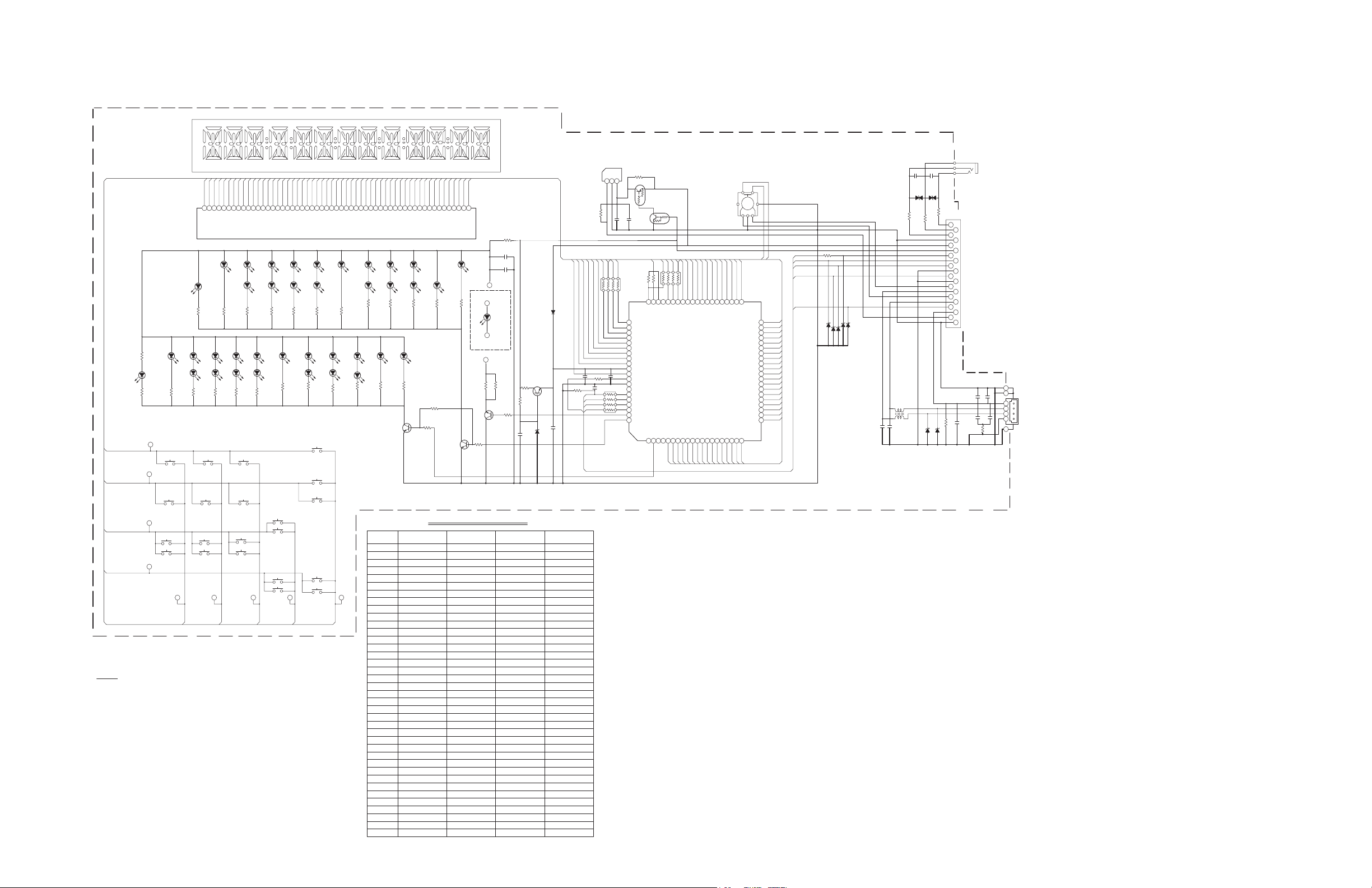
SML-D12V8WT
SML-D12V8WT
RK73FB2B122J
RK73FB2B621J
RK73FB2B821J
QSMR-C13SBCMN
RK73FB2B122J RK73FB2B821J
RK73FB2B621J
SML-D12V8WT
DZ2J056M
SML-D12V8WT
RK73FB2B821J
RK73FB2B122J
SML-D12V8WT
SML-D12V8WT
R23
RK73FB2B621J
D35
reference
-
XJ6-0393-20
D92
QSMR-C13SBCMN
QSMR-C13SBCMN
RK73FB2B821J
R27
R26
SML-D12V8WT
QSMR-C13SBCMN
QSMR-C13SBCMNQSMR-C13SBCMN
RK73FB2B821J
QSMR-C13SBCMN
QSMR-C13SBCMN
-
QSMR-C13SBCMN
CK73GBB1H471K
SML-D12V8WT
XJ6-0393-21
RK73FB2B122J
SML-D12V8WT
RK73FB2B821J
CK73GBB1H472K
CK73GBB1H471K
SML-D12V8WT
SML-D12V8WT
XJ6-0363-20
RK73FB2B821J
R29
C86
RK73FB2B821J
RK73FB2B821J
D22
QSMR-C13SBCMN
QSMR-C13SBCMN
D37
-
RK73FB2B122J
D24
-
SML-D12V8WT
R20
QSMR-C13SBCMN
RK73FB2B821J
QSMR-C13SBCMN
D33
D38
D30
D41
-
SML-D12V8WT
QSMR-C13SBCMN
SML-D12V8WT
QSMR-C13SBCMN
R19
RK73FB2B122J
RK73FB2B621J
D20
RK73FB2B821J
-
-
SML-D12V8WT
SML-D12V8WT
R25
SML-D12V8WT
B3H-0006-00
QSMR-C13SBCMN
RK73FB2B821J
QSMR-C13SBCMN SML-D12V8WT
-
USB-BT BLUE REMO
RK73FB2B821J
QSMR-C13SBCMN
SML-D12V8WT
SML-D12V8WT
SML-D12V8WT
D91
SML-D12V8WT
CK73GBB1H472K
SML-D12V8WT
QSMR-C13SBCMN
CK73GBB1H471K
QSMR-C13SBCMN
RK73FB2B621JR24
-
RK73FB2B821J
D31
RK73EB2E000J
R22
- CK73GBB1H471K
SML-D12V8WT
RK73FB2B122J
SML-D12V8WT
-
RK73FB2B621J
XJ6-0393-22
SML-D12V8WT
R30
RK73FB2B821J
QSMR-C13SBCMN
D34
USB RED REMO
B3H-0009-00
SML-D12V8WT
SML-D12V8WT
D39
SML-D12V8WT
-
RK73FB2B821J
*
C7
SML-D12V8WT
B3H-0006-00
RK73FB2B621J
RK73FB2B122J
RK73FB2B621J
QSMR-C13SBCMN
QSMR-C13SBCMN
RK73FB2B821J
SML-D12V8WT
-
QSMR-C13SBCMN
DZ2J056M
QSMR-C13SBCMN
RK73FB2B621J
RK73FB2B821J
D28
QSMR-C13SBCMN
D25
RK73FB2B821J
R28
D36
SML-D12V8WT
B3H-0006-00
QSMR-C13SBCMN
RK73FB2B621J
R81
DMR ENTRY RED REMO
D26
RK73FB2B621J
-
RK73FB2B621J
QSMR-C13SBCMN
-
DZ2J056M
QSMR-C13SBCMN
QSMR-C13SBCMN
RK73FB2B621J
RK73FB2B821J
R21
QSMR-C13SBCMN
RK73FB2B621J
RK73FB2B821J
C85
DMR-BT BLUE REMO
DZ2J056M
QSMR-C13SBCMN
SML-D12V8WT
RK73FB2B821JRK73FB2B122J
QSMR-C13SBCMN
QSMR-C13SBCMN
SML-D12V8WT
SML-D12V8WT
SML-D12V8WT
SML-D12V8WT
RK73EB2E000J
D40
QSMR-C13SBCMN
DIFFERENCE TABLE
RK73FB2B821J
QSMR-C13SBCMN
-
QSMR-C13SBCMN
D29
D27
ED1
3. COMPONENTS WITH ? IN FRONT INDICATE NOT USE.
2.
ALL RESISTANCE VALUES ARE IN OHM.
1. VOLTAGES ARE DC-MEASURED WITH A DIGITAL VOLT METER WITHOUT INPUT SIGNAL
UNLESS OTHERWISE SPECIFIED.
NOTES
ALL RESISTORS ARE 1/10W +5% METAL GLAZE RESISTOR.
ALL CAPACITANCE VALUES ARE IN uF(P=pF)
ALL CAPACITORS ARE 50V OR 25V CERAMIC CAPACITOR.
ALL E.CAPACITORS ARE SHOWN IN THE FORM OF CAPACITANCE(uF)/RATED VOLTAGE(V)
5.6V
9.4v
5.0V
F_AUXG
J7J-0033-**
0V
0V
0V
0.7V
0.6V
1.7V
3.3V
0V
3.2V
0V
0V
0V
0V
2.5V
2.5V
2.5V
2.5V
2.5V
5.0V
2.5V
0V
1.8V
0V
2.0V
0.2V
3.3V
4.8V
4.0V
4.0V
2.5V
2.5V
2.5V
2.5V
2.5V
2.5V
2.5V
2.5V
2.5V
2.5V
2.5V
2.5V
2.5V
2.5V
2.5V
2.5V
2.5V
2.5V
2.5V
2.5V
2.5V
2.5V
2.5V
2.5V
2.5V
2.5V
2.5V
2.5V
2.5V
2.5V
2.5V
2.5V
2.5V
2.5V
2.5V
2.5V
2.5V
2.5V
2.5V
2.5V
2.5V
2.5V
2.5V
2.5V
2.5V
2.5V
2.5V
2.5V
2.5V
2.8V
2.8V
2.8V
2.8V
2.8V
2.8V
PAN_DET
LCD_INH
LCD_CLK
LCD_DATA_LCD
LCD_CE
Duo
SWITCH PWB: J7J-0113-**
LCD_DATA_SYS
EJECT
DISP/SETUP
EASY EQ
PWR/SRC
1
FORWARD
FOLDER DOWN
IPOD/USB/PHONE
3/ FOLDER UP
4/RNDM
6
BACKWARD
2/
5/RPT
BACK/SEARCH
single
USB_GND
USB_GND
GND
F_AUXR
USB5V
REMO
ENC2
ENC1
ILM_10.5
LCD_DATOUT
F_AUXL
KS3
KI3
KI4
KI2
KI1
KS6
KI5
KS2
PANEL_3.3V
KS1
D-
D+
LCD_CLK
LCD_DATIN
LCD_CE
LCD_INH
KS6
LCD_DATOUTLCD_DATIN
COM4
COM3
COM2
COM1
S51
S50
S49
S48
S47
S46
S45
S44
S43
S42
S41
S40
S39
S37
S38
S36
S35
S34
S33
S32
S31
S30
S29
S28
S27
S26
S25
S24
S23
S22
S21
S20
S19
S18
S17
S16
S15
S14
S13
S12
S11
S10
S9S8S7S6S5S4S3S2S1
LCD_INH
LCD_CE
LCD_CLK
KS1
KS2
KS3
KI1
S49
KS1
KI4
S51
S50
COM4
COM3
COM2
COM1
S37
S38
S39
S40
S41
S42
S43
S44
S45
S46
S47
S48
S1S2S3S4S5S6S7S8S9
S10
S11
S12
S13
S14
S15
S16
KI5
KI4
KI3
KI2
S36
S35
S34
S33
S32
S31
S30
S29
S28
S27
S26
S25
S24
S23
S22
S21
S20
S19
S18
S17
TL2-2
TL1-2
TL1-1
TL3 TL4 TL5
TL6
TL7
TL8
TL9
TL10
TL11
TL2-1
S1A
S13S12
S4
S6
S3
S9
S15
S7
S2A
S1
S5
S2
S11A
S11
S5A
S6A
S8
S14
S4AS3A
RK74GB1J101J
1/16W100
RA2
RK74GB1J101J
1/16W100
RA1
RK74GB1J101J
1/16W
100
RA3
1/10W 0
*R81
1/4W220
R80
1/8W4.7
R62
1/8W100
R60
1/8W100
R61
1/4W100
R1
0
?R1009
1/8W750
?R18
1/8W750
?R41
1/8W750
?R37
1/8W750
?R32
1/8W560
?R38
1/8W560
?R39
1/8W560
?R40
1/8W560
?R35
1/8W560
?R34
1/8W560
?R36
1/8W560
?R33
1/8W560
?R31
8201/8W
*R19
8201/8W
*R30
6201/8W
*R29
6201/8W
*R28
6201/8W
*R27
8201/8W
*R26
6201/8W
*R25
6201/8W
*R24
620
1/8W
*R23
6201/8W
*R22
8201/8W
*R21
820
1/8W
*R20
1/4W
0
R1000
1/10W
?R91
1k
?R56
1/8W560
R55
0
R1006
1/10W0
?R1010
100
R4
47k
?R2
470
R3
4.3k
4.3k
R51
4.3k
R50
4.3k
?R53
1k
R6
1/4W
0
R7
1/4W
330
R5
?Q90
C
B
E
?Q91
LSCR523EBFS8
Q1
2SC4097P/R/
Q51
LSCR523EBFS8
Q50
?Q53
NQR0704-001X
FL80
7 6
5 4
3 21
T9K-0007-00
S20
15
8
5
18
11
214
717
10 420
13 1
616
9 319
12
CN1
QGZ2006K1-20X
7 65
VCC
4
D-
3
D+
2
GND
1
QNZ1076-001
J80
3
2
1
QNS0279-001
J60
S2/P2/G280
S1/P1/G179
SDI78
SCL77
SCE76
INHB75
OSC/S6974
VSS73
SDO72
S6871
VDD70
S6769
COM468
COM367
COM266
COM165
KI5/S6664
KI4/S6563
KI3/S6462
KI2/S6361
KI1/S62
60
KS6/S6159KS5/S6058KS4/S5957KS3/S5856KS2/S5755KS1/S56
54
S5553S5452S5351S5250S5149S5048S4947S4846S4745S4644S4543S4442S43
41
S42 40
S41 39
S40 38
S39 37
S38 36
S37 35
S36 34
S35 33
S34 32
S33 31
S32 30
S31 29
S30 28
S29 27
S28 26
S27 25
S26 24
S25 23
S24 22
S23 21
S2220S2119S2018S1917S1816S1715S1614S1513S1412S1311S1210S119S108S97S86S75S6/P6/G64S5/P5/G53S4/P4/G42S3/P3/G3
1
BU97520AKV-M
IC1
VCC3GND2OUT
1
SIR8630B6T
IC90
555453525150494847464544434241401 2 3 4 5 6 7 8 9 10 11 12 13 14 15 16 17 18 19 20 21 22 23 24 25 26 27 28 29 30 31 32 39383736353433
*ED1
VOL
*D31
BACK
*D28
?D66?D54 ?D64
EQ
*D40
?D70?D63
?D67
?D59 ?D61?D55
?D68
?D65
?D58
?D57
?D71?D52
FWD
*D24
DISP
*D29
VOL
*D30
?D56 ?D60
?D69
SOURCE
*D41
4
*D37
2
*D35
5
*D38
VOL
*D33
FWD
*D25
1
*D343*D36
EJECT
*D22
6
*D39
BWD
*D27
BWD
*D26
?D50
ACCENT
*D20
BACKLIGHT
LUWJNSH.PC//0
D49
?D11 ?D10
DZ2J056M
D1
?D93
?D90
?D94
DZ2J051M
D81
DZ2J051M
D80
DZ2J056M
*D91
DZ2J056M
*D92
MBRX130
D2
1u
C1
?C2
1u
?C4
1u
C5
10u
C6
27p
C80
27p
C81
10u
C82
4700p
C84
470p
470p
C83
1u
C91
?C90
4700p
*C85
470p
*C86
1u
470p
*C7
1000p
C60
1000p
C61
470p
C3
SWITCH PWB ASSY (XJ6-0393-21) KD-X220UR
CN701
KD-X220UR
(XJ1-0503-20)
To MAIN PWB ASSY
AUX
USB
created date:2015-04-22No.MA606
22
(No.MA606<Rev.002>)10/
Page 31

MAIN PWB ASSY XJ1-049x-xx (J7J-0022-10) Except KD-X220UR
(Lead free solder used in the board (material : Sn-Cu, melting point : 230 Centigrade))
(Lead free solder used in the board (material : Sn-Ag-Cu, melting point : 219 Centigrade))
1
1
1
1
1
1
1
1
1
1
1
1
A
B
C
1
C
B
A
1
1
J7J-0022-10
XJ1-041
XJ1-049
XJ1-050
1
1
1
1
1
1
1
1
1
1
R1069
W427
Q471
Q470
R1079
C1074
R1091
R1082
C226
R240
R224
R239
D222
Q220
W533
R431
R1430
C1096
R1428
R1425
CN228
R1077
C1070
R1432
R1075
C1057
R1074
R1419
R1426
R1170
R1416
R1415
R1414
R1410
D473
D474
D475
R1408
CN701
W405
W404
W403
W402
W401
R1052
C1052
R229
R228
C222
R223
R221
J220
C221
C227
C220
R222
L223
C224
C223
L220
R816
C854
R241
R777
R776
R775
R179
R178
R233
R979
R969
R980
R978
C877
R371
R380
C341
C351
C331
C321
C251
C261
C308C307
C310
C309
C614
IC601
R607
R611
C621
C612
X600
C618C616
L607
R609
R601
C626
C613
R608
C623
C619
C610
C615
C620
D601
R610
R605
C609
L608
C622
R13
C611
C603
L606
D602
C602
L605
C604
R606
J600
C617
R757
R759
R756
R755
R753
R754
R779
R778
L785
R572
R573
R571
R574
R765
R766
R103
R102
R101
R719
R760
R482
C627
R230
R272
C624
C1056
C1064
D1061
D1060
R483
C1066
C1079
C1078
D472
R1404
R1405
R781
C318
C319
C317
C316
C727
L611
R746
R747
R700
X540
C721
R720R710
C722
R752
R751
C576
L591
C574
C575
C573
C572
C571
C598
R589
C589
R598
C588
C599
R599
R588
IC555
R1007
C908
C172
L610
C630
R1073
R1072
D391
D390
C909
C1094
L709
L822
L823
L820
L824
L821
R1070
R1022
R1411
D861
R171
C1098
C1021
C1020
Q271
R970
C869
L861
R865
C860
R867
C868
C864
C1097
R864
C865
R868
C861
C863
L860
C866
R869
IC861
R861
R866
C862
R862
C870
C1077
C1076
R471R745
C1068
R1002
R1001
R1000
R705
R353
D224
R243
R1093
C920
IC901
R401
C821
Q273
C723
C725
C724
D223
R1071
D272
R472
D273
C1001
L701
C225
R365
Q360
C360
C361
R360
R361
R717
L827
L825
Q260
L826
Q701
D400
D401
C905
C930
C390
C171
C1050
C904
IC821
C830
R930
C867
R750
D271
D270
D370
L1000
Q270
Q330
Q350
Q320
Q340
Q250
IC851
IC161
C100
R470
R476
R721
R253
R164
R100
R703
R704
R707
R722
R370
R473
R723
R819
R744
R821
R105
R739
R820
R733
R734
R1090
R706
R373
R732
R743
R273
R740
R822
R735
R741
R730
R104
R702
R414
R413
R412
R323
R343
R271
R333
R262
R252
R840
R841
R402
R251
R351
R261
R932
R321
R331
R341
R302
R716
R167
R725
R726
R728
R340
R260
R320
R350
R250
R330
R727
R729
R724
R270
R713
R715
R372
R714
R712
R931
R400
R168
R410
R477
R1003
R478
R411
R169
R701
R474
R475
R162
R1060
R403
R390
R711
R381
R170
R307
D380
D381
Q930
Q272
C380
C1090
C710
C820
C410
C1015
C1000
C1017
C832
C711
C1016
C1014
C166
C831
C931
C370
C822
C101 C102
C840
C850
C105
C104
C103
C475
C473
C474
C170
C177
C167
C161
C169
C162
C168
C311
C391
C392
C304
C907
C330
C340
C350
C250
C320
C260
C707
C708
Q931
D990
IC841
IC831
IC301
IC411
X701
C852
C165
C890
C163
C164
C990
J321
CN990
J470
L990
S830
IC701
D101
D100
C1095
R432
C726
J601
R1434
W422
W420
L780
MARK
UL
W
K
created date:2015-04-22No.MA606
22
(No.MA606<Rev.002>)11/
Page 32

How to repair a fuse pattern.
Refer to "2.1 How to repair a fuse pattern".
1
1111
1
SXI.R
SXI.L
AR
AL
TU.L
TU.R
IP4
IP3
IP2 IP1
DIST
AC
TM
RXM
TXM
ASEBRK
ASEMD
TRST
TCK
TMS
TDI
TDO
VDD
CS
DI
WP
RST2 RST1
HOLD
GND2
GND1
DO
CLK
OE
REM
A.ANT
PDET
FLG
V6I
HSSIN
EXT
ANT
C1080
R1080
C1073
C1072
C1071
R1055
C1055
R1429
R1424
R1076
C1075
R1421
R1417
C894
CN701
R1407
R1406
FMIN
R1051
C1051
R231
R232
J220
R227
L221
VDD5V
BT_RST
MICP
L222
R226
DGND
AGND
BT_L
BT_R
A9V
R225
MICN
USB_5V
D+
CE
V10.5
D-
AG
GND
5V/INH
C1040
USBG
VOL1
D471
D470
C470
R603
C608
SCL
C605
L602
L601
L604
C600
VA600
R602
R600
C607
L603
C601
C1091
SDA
L600
C606
R604
J600
D903
VA601
C1003
R1006
R1005
C1084
VA1400
C1085
C1089
R1018
C1018
C1088
C1065
L609
C1067
R1004
D1401
DIMMER_IN
C851
R758
L758
C912
C913
C172
C1093
C911
R1061
C868
DB1C
DB1B
DB1A
D1402
R612
C853
C1092
D902
IC901
C1069
R362
D360
R364
R363
C905
R890
IC891
L850
C314
R891
R742
R304
R749
R892
R830
R303
C718
C1012
C472
C717
C1002
C701
C706
C1010
C700
C709
C703
C716
C1011
C892
C704
C702
C891
C1013
C713
C712
C705
C471
C906
C313
C304
C907
C303
C305
C306
D990
IC301
C852
C165
C890
DAC.R
C163
C164
DAC.L
C990
J321
CN990
J470
L990
S830
FL
RR
SUBL
J601
TU33
SW33
P33
V1.25
VDD
AUD
ERR1
DAC5
TMUTE
SUBR
ILM
BUP
MEM
RL
C1082
MAIN PWB ASSY XJ1-049x-xx (J7J-0022-10) Except KD-X220UR
(Lead free solder used in the board (material : Sn-Cu, melting point : 230 Centigrade))
(Lead free solder used in the board (material : Sn-Ag-Cu, melting point : 219 Centigrade))
created date:2015-04-22No.MA606
22
(No.MA606<Rev.002>)12/
Page 33

MAIN PWB ASSY XJ1-0503-20 (J7J-0022-20) KD-X220UR
(Lead free solder used in the board (material : Sn-Cu, melting point : 230 Centigrade))
(Lead free solder used in the board (material : Sn-Ag-Cu, melting point : 219 Centigrade))
1
1
1
1
1
1
1
1
1
1
1
1
A
B
C
1
C
B
A
XJ1-096
XJ1-093
J7J-0022-20
1
1
XJ1-041
XJ1-049
XJ1-050
1
1
1
1
1
1
1
1
1
1
R1069
W427
Q471
Q470
R1079
C1074
R1091
R1082
C226
R240
R224
R239
D222
Q220
W533
R431
R1430
C1096
R1428
R1425
CN228
R1077
C1070
R1432
R1075
C1057
R1074
R1419
R1426
R1170
R1416
R1415
R1414
R1410
D473
D474
D475
R1408
CN701
W405
W404
W403
W402
W401
R1052
C1052
R229
R228
C222
R223
R221
J220
C221
C227
C220
R222
L223
C224
C223
L220
R816
C854
R241
R777
R776
R775
R179
R178
R233
R979
R969
R980
R978
C877
R371
R380
C341
C351
C331
C321
C251
C261
C308C307
C310
C309
C614
IC601
R607
R611
C621
C612
X600
C618C616
L607
R609
R601
C626
C613
R608
C623
C619
C610
C615
C620
D601
R610
R605
C609
L608
C622
R13
C611
C603
L606
D602
C602
L605
C604
R606
J600
C617
R757
R759
R756
R755
R753
R754
R779
R778
L785
R572
R573
R571
R574
R765
R766
R103
R102
R101
R719
R760
R482
C627
R230
R272
C624
C1056
C1064
D1061
D1060
R483
C1066
C1079
C1078
D472
R1404
R1405
R781
C318
C319
C317
C316
C727
L611
R746
R747
R700
X540
C721
R720R710
C722
R752
R751
C576
L591
C574
C575
C573
C572
C571
C598
R589
C589
R598
C588
C599
R599
R588
IC555
R1007
C908
C172
L610
C630
R1073
R1072
D391
D390
C909
C1094
L709
L822
L823
L820
L824
L821
R1070
R1022
R1411
D861
R171
C1098
C1021
C1020
Q271
R970
C869
L861
R865
C860
R867
C868
C864
C1097
R864
C865
R868
C861
C863
L860
C866
R869
IC861
R861
R866
C862
R862
C870
C1077
C1076
R471R745
C1068
R1002
R1001
R1000
R705
R353
D224
R243
R1093
C920
IC901
R401
C821
Q273
C723
C725
C724
D223
R1071
D272
R472
D273
C1001
L701
C225
R365
Q360
C360
C361
R360
R361
R717
L827
L825
Q260
L826
Q701
D400
D401
C905
C930
C390
C171
C1050
C904
IC821
C830
R930
C867
R750
D271
D270
D370
L1000
Q270
Q330
Q350
Q320
Q340
Q250
IC851
IC161
C100
R470
R476
R721
R253
R164
R100
R703
R704
R707
R722
R370
R473
R723
R819
R744
R821
R105
R739
R820
R733
R734
R1090
R706
R373
R732
R743
R273
R740
R822
R735
R741
R730
R104
R702
R414
R413
R412
R323
R343
R271
R333
R262
R252
R840
R841
R402
R251
R351
R261
R932
R321
R331
R341
R302
R716
R167
R725
R726
R728
R340
R260
R320
R350
R250
R330
R727
R729
R724
R270
R713
R715
R372
R714
R712
R931
R400
R168
R410
R477
R1003
R478
R411
R169
R701
R474
R475
R162
R1060
R403
R390
R711
R381
R170
R307
D380
D381
Q930
Q272
C380
C1090
C710
C820
C410
C1015
C1000
C1017
C832
C711
C1016
C1014
C166
C831
C931
C370
C822
C101 C102
C840
C850
C105
C104
C103
C475
C473
C474
C170
C177
C167
C161
C169
C162
C168
C311
C391
C392
C304
C907
C330
C340
C350
C250
C320
C260
C707
C708
Q931
D990
IC841
IC831
IC301
IC411
X701
C852
C165
C890
C163
C164
C990
J321
CN990
J470
L990
S830
IC701
D101
D100
C1095
R432
C726
J601
R1434
W422
W420
L780
MARK
UL
W
K
created date:2015-04-22No.MA606
22
(No.MA606<Rev.002>)13/
Page 34

How to repair a fuse pattern.
Refer to "2.1 How to repair a fuse pattern".
1
1111
1
SXI.R
SXI.L
AR
AL
TU.L
TU.R
IP4
IP3
IP2 IP1
DIST
AC
TM
RXM
TXM
ASEBRK
ASEMD
TRST
TCK
TMS
TDI
TDO
VDD
CS
DI
WP
RST2 RST1
HOLD
GND2
GND1
DO
CLK
OE
REM
A.ANT
PDET
FLG
V6I
HSSIN
EXT
ANT
C1080
R1080
C1073
C1072
C1071
R1055
C1055
R1429
R1424
R1076
C1075
R1421
R1417
C894
CN701
R1407
R1406
FMIN
R1051
C1051
R231
R232
J220
R227
L221
VDD5V
BT_RST
MICP
L222
R226
DGND
AGND
BT_L
BT_R
A9V
R225
MICN
USB_5V
D+
CE
V10.5
D-
AG
GND
5V/INH
C1040
USBG
VOL1
D471
D470
C470
R603
C608
SCL
C605
L602
L601
L604
C600
VA600
R602
R600
C607
L603
C601
C1091
SDA
L600
C606
R604
J600
D903
R894
C893
VA601
C1003
R1006
R1005
C1084
VA1400
C1085
C1089
R1018
C1018
C1088
C1065
L609
C1067
R1004
D1401
DIMMER_IN
C851
R758
L758
C912
C913
C172
C1093
C911
R1061
C868
DB1C
DB1B
DB1A
D1402
R612
C853
C1092
D902
IC901
C1069
R362
D360
R364
R363
C905
R890
IC891
L850
C314
C1099
R742
R304
R749
R892
R830
R303
C718
C1012
C472
C717
C1002
C701
C706
C1010
C700
C709
C703
C716
C1011
C892
C704
C702
C891
C1013
C713
C712
C705
C471
C906
C313
C304
C907
C303
C305
C306
D990
IC301
C852
C165
C890
DAC.R
C163
C164
DAC.L
C990
J321
CN990
J470
L990
S830
FL
RR
SUBL
J601
TU33
SW33
P33
V1.25
VDD
AUD
ERR1
DAC5
TMUTE
SUBR
ILM
BUP
MEM
RL
C1082
MAIN PWB ASSY XJ1-0503-20 (J7J-0022-20) KD-X220UR
(Lead free solder used in the board (material : Sn-Cu, melting point : 230 Centigrade))
(Lead free solder used in the board (material : Sn-Ag-Cu, melting point : 219 Centigrade))
created date:2015-04-22No.MA606
22
(No.MA606<Rev.002>)14/
Page 35

SWITCH PWB ASSY-1 XJ6-031x-xx (J7J-0033-00) Except KD-X220UR
(Lead free solder used in the board (material : Sn-Cu, melting point : 230 Centigrade))
(Lead free solder used in the board (material : Sn-Ag-Cu, melting point : 219 Centigrade))
S2A
ED1
S3A
S11A
S5A
S6A
S4A
S1A
R1010
D60
D56
D30
D29
D22
D20
D52
D71
D50
D57
D58
D65
D68
D55
D61
D59
D67
D69
D63
D70D64
D54
D66
S20
D28
D31
D36
D39
D27
D26
D24
D34
D25
D33
D38
D35
J60
IC90
S14 S15S12
S3
S9
S11
S7
S13
S8
S4
S5
S6
S1
S2
J80
D37D41 D40
created date:2015-04-22No.MA606
22
(No.MA606<Rev.002>)15/
Page 36

1
XJ6-040
XJ6-039
XJ6-031
J7J-0033-00
1
A/2
R64
R63
D11
D10
R56
C7
R1000
R81
KS6
KS3
KS2
KS1
KI5
W
K
MARK
UL
R55
R1006
CN1
KI4
R18
D94
D93
D92
D91
D90
R19
Q53
R53
R30
R29 R28
R27
R26
R25
R24
R23
R22
KI3
R91
KI2
R21
R20
R35
R37
R32
R31
R40 R39
R33
R38
R34
R36
R41
S20
Q51
RA1
RA3
RA2
R51
R2
R3
R50
KI1
C86
R80
R6
R4
R1
R62
R61
R60
R5
R1005
R7
C60
C61
C83 C84
C3
C2
C6
C82
C81
C80
C90
C91
J60
Q91
Q90
C1
C5
C4
C85
C87
R1009
IC90
J80
FL80
L1
L2
D2
D3
Q50
Q1
D1
D80
D81
IC1
SWITCH PWB ASSY-1 XJ6-031x-xx (J7J-0033-00) Except KD-X220UR
(Lead free solder used in the board (material : Sn-Cu, melting point : 230 Centigrade))
(Lead free solder used in the board (material : Sn-Ag-Cu, melting point : 219 Centigrade))
created date:2015-04-22No.MA606
22
(No.MA606<Rev.002>)16/
Page 37

SWITCH PWB ASSY-2 XJ6-031x-xx (J7J-0033-00) Except KD-X220UR
(Lead free solder used in the board (material : Sn-Cu, melting point : 230 Centigrade))
(Lead free solder used in the board (material : Sn-Ag-Cu, melting point : 219 Centigrade))
XJ6-040
D49
created date:2015-04-22No.MA606
22
(No.MA606<Rev.002>)17/
Page 38

XJ6-039
XJ6-031
J7J-0033-00
B/2
MARK
UL
SWITCH PWB ASSY-2 XJ6-031x-xx (J7J-0033-00) Except KD-X220UR
(Lead free solder used in the board (material : Sn-Cu, melting point : 230 Centigrade))
(Lead free solder used in the board (material : Sn-Ag-Cu, melting point : 219 Centigrade))
created date:2015-04-22No.MA606
22
(No.MA606<Rev.002>)18/
Page 39

SWITCH PWB ASSY-1 XJ6-0393-21 (J7J-0033-00) KD-X220UR
(Lead free solder used in the board (material : Sn-Cu, melting point : 230 Centigrade))
(Lead free solder used in the board (material : Sn-Ag-Cu, melting point : 219 Centigrade))
S2A
ED1
S3A
S11A
S5A
S6A
S4A
S1A
R1010
D60
D56
D30
D29
D22
D20
D52
D71
D50
D57
D58
D65
D68
D55
D61
D59
D67
D69
D63
D70D64
D54
D66
S20
D28
D31
D36
D39
D27
D26
D24
D34
D25
D33
D38
D35
J60
IC90
S14 S15S12
S3
S9
S11
S7
S13
S8
S4
S5
S6
S1
S2
J80
D37D41 D40
created date:2015-04-22No.MA606
22
(No.MA606<Rev.002>)19/
Page 40

1
XJ6-040
XJ6-039
XJ6-031
J7J-0033-00
1
A/2
R64
R63
D11
D10
R56
C7
R1000
R81
KS6
KS3
KS2
KS1
KI5
W
K
MARK
UL
R55
R1006
CN1
KI4
R18
D94
D93
D92
D91
D90
R19
Q53
R53
R30
R29 R28
R27
R26
R25
R24
R23
R22
KI3
R91
KI2
R21
R20
R35
R37
R32
R31
R40 R39
R33
R38
R34
R36
R41
S20
Q51
RA1
RA3
RA2
R51
R2
R3
R50
KI1
C86
R80
R6
R4
R1
R62
R61
R60
R5
R1005
R7
C60
C61
C83 C84
C3
C2
C6
C82
C81
C80
C90
C91
J60
Q91
Q90
C1
C5
C4
C85
C87
R1009
IC90
J80
FL80
L1
L2
D2
D3
Q50
Q1
D1
D80
D81
IC1
SWITCH PWB ASSY-1 XJ6-0393-21 (J7J-0033-00) KD-X220UR
(Lead free solder used in the board (material : Sn-Cu, melting point : 230 Centigrade))
(Lead free solder used in the board (material : Sn-Ag-Cu, melting point : 219 Centigrade))
created date:2015-04-22No.MA606
22
(No.MA606<Rev.002>)20/
Page 41

SWITCH PWB ASSY-2 XJ6-0393-21 (J7J-0033-00) KD-X220UR
(Lead free solder used in the board (material : Sn-Cu, melting point : 230 Centigrade))
(Lead free solder used in the board (material : Sn-Ag-Cu, melting point : 219 Centigrade))
XJ6-040
D49
created date:2015-04-22No.MA606
22
(No.MA606<Rev.002>)21/
Page 42

XJ6-039
XJ6-031
J7J-0033-00
B/2
MARK
UL
SWITCH PWB ASSY-2 XJ6-0393-21 (J7J-0033-00) KD-X220UR
(Lead free solder used in the board (material : Sn-Cu, melting point : 230 Centigrade))
(Lead free solder used in the board (material : Sn-Ag-Cu, melting point : 219 Centigrade))
created date:2015-04-22No.MA606
22
(No.MA606<Rev.002>)22/
Page 43

PARTS LIST
20
DIGITAL MEDIA RECEIVER
KD-X120EE KD-X120EU KD-X120U
KD-X120UT KD-X125EE KD-X220E
KD-X220EN KD-X220EY KD-X220J
KD-X220U KD-X220UR KD-X220UT
(No.MA606<Rev.002>)1/
Page 44

■ PRECAUTIONS ON SCHEMATIC DIAGRAMS
z Due to the improvement in performance, some part numbers shown in the circuit diagrams
may not agree with those indicated in the Parts List.
z The parts numbers, values and rated voltage etc. in the Schematic Diagrams are for
reference only.
z Since the circuit diagrams are standard ones, the circuits and circuit constants may be
subject to change for improvement without any notice.
■ PRECAUTIONS ON PARTS LIST
z
The parts identified by the symbol are critical for safety. Whenever replacing these parts, be sure to
use specified ones to secure the safety.
z
The parts not indicated in this Parts List and those which are filled with lines --- in the Parts No.
columns will not be supplied.
z
P.W. BOARD Ass'y will not be supplied, but those which are filled with the Parts No. in the Parts No.
columns will be supplied.
z
When ordering chips, screws etc., place bulk orders (unit of tens) whenever possible to improve
shipping efficiency.
z
There are cases where the actual implemented parts in the sets and the service parts are different.
When ordering parts, make sure to refer to the Parts List.
■
PRECAUTIONS ON SERVICE
Certain parts of the power circuits and the GNDs differ according to the models. Care must be
taken for the following points as the differences are indicated separately in the LIVE GND ( ) and
the ISOLATED (NEUTRAL) GND ( ).
1. Do not touch the LIVE GND, or do not touch the LIVE GND and the ISOLATED (NEUTRAL)
GND at the same time. It may cause an electric shock.
Before pulling out the chassis or other parts, make sure to pull out the power cord from the
wall outlet first.
2. Do not short circuit between the LIVE GND and ISOLATED (NEUTRAL) GND, or never
measure the LIVE GND and ISOLATED (NEUTRAL) GND at the same time using measuring
instruments (oscilloscope, etc.). It may blow fuses or damage other parts.
■ DEVIATION TOLERANCE RANGE
DEVIATION TOLERANCE RANGE
F G J K M N R H Z P
± 1% ± 2% ± 5% ±10% ±20% ±30%
+30%
-10%
+50%
-10%
+80%
-20%
+100%
-0%
20
(No.MA606<Rev.002>)2/
Page 45

RC1
PA1
LCD1
H
G
F901
F
E
DC2
DC1
D
C
C
C
B
B
A
A
A
A
503
502
501
356
355
354
353
273
269
268
267
266
265
264
262
258
256
254
253
252
251
218
217
216
215
213
,
,
,
702
771
770
x2
701
x2
x2
(MAIN)
712
711
772
719
(SWITCH)
Parts with the exploded numbers larger than 700 are not supplied.
Block No.M1MM
EXPLODED VIEW
created date:2015-04-22No.MA606
20
(No.MA606<Rev.002>)3/
Page 46

MODEL MARK MODEL MARK MODEL MARK MODEL MARK
20
KD-X120EE A KD-X120EU B KD-X120U C KD-X120UT D
KD-X125EE E KD-X220E F KD-X220EN G KD-X220EY H
KD-X220J I KD-X220U J KD-X220UR K KD-X220UT L
Safe Symbol No. Parts No. Parts Name Description QTY Local
EXPLODED VIEW <M1MM>
DC1 QAM1329-001 DC DORD 1 B,C,D,I,J,L
DC2 QAM1345-003 DC DORD 1 A,E,F,G,H
DC2 QAM1378-001 DC DORD 1 K
! F901 FZB10BT-100 BLADE FUSE 1
LCD1 B3H-0006-00 LCD 1
PA1 A6D-0021-00 PANEL 1 A,B,C,D,E,F,G,H,I,J,
PA1 A6D-0021-04 PANEL 1 K
RC1 RM-RK52M REMOTE CONTROL UNI 1 C,D,I,J,K,L
A QYSDSF2008ZA TAP SCREW M2 x 8mm 4
B GE40377-002A SPECIAL SCREW 2
C QYSDST2606ZA TAP SCREW M2.6 x 6mm 3
D QYSDST2610ZA TAP SCREW M2.6 x 10mm 1
E QYSDST2608ZA TAP SCREW M2.6 x 8mm 2
F GE40377-005A SPECIAL SCREW 2
G QYSDSG3006ZA TAP SCREW M3 x 6mm 1 A,B,C,D,E,F,G,H,I,J,
G QYSPSG3008ZA TAP SCREW M3 x 8mm 1 K
H QYSDSF2608ZA TAP SCREW M2.6 x 8mm 1
213 A2C-0006-00 SUB PANEL 1 A,E,F,G,H,I
213 A2C-0006-01 SUB PANEL 1 B,C,D,J,L
213 A2C-0006-02 SUB PANEL 1 K
215 GE35609-001A LOCK LEVER 1
216 GE40514-004A TORSION SPRING 1
217 GE35611-001A RELEASE LEVER 1
218 GE30999-014A COMP.SPRING 1
251 F0G-0011-00 COVER USB DOOR 1 A,B,C,D,E,F,G,H,I,J,
251 F0G-0011-01 COVER USB DOOR 1 K
252 B1A-0014-02 FRONT GLASS 1 A
252 B1A-0014-01 FRONT GLASS 1 B,C,D
252 B1A-0014-03 FRONT GLASS 1 E
252 B1A-0014-06 FRONT GLASS 1 F,G,H
252 B1A-0014-04 FRONT GLASS 1 I
252 B1A-0014-05 FRONT GLASS 1 J,L
252 B1A-0014-0A FRONT GLASS 1 K
253 K2F-0012-00 PUSH KNOB SEARCH BTN 1 A,B,C,D,E,F,G,H,I,J,
253 K2F-0012-01 PUSH KNOB SEARCH BTN 1 K
254 K2F-0014-00 PUSH KNOB FN BTN 1 A,B,C,D,E
254 K2F-0014-01 PUSH KNOB FN BTN 1 F,G,H,I,J,L
254 K2F-0014-04 PUSH KNOB FN BTN 1 K
256 K2E-0008-00 PUSH KNOB SRC BTN 1 A,B,C,D,E,F,G,H,I,J,
256 K2E-0008-01 PUSH KNOB SRC BTN 1 K
258 K2F-0013-00 PUSH KNOB PRESET BTN 1 A,B,C,D,E,F,G,H,I,J,
258 K2F-0013-01 PUSH KNOB PRESET BTN 1 K
262 K2E-0009-00 PUSH KNOB DETACH BTN 1 A,B,C,D,E,F,G,H,I,J,
262 K2E-0009-02 PUSH KNOB DETACH BTN 1 K
264 GE30999-012A COMP.SPRING 1
265 K2K-0102-03 KNOB VOL KNOB 1 A,B,C,D,E
265 K2K-0102-00 KNOB VOL KNOB 1 F,G,H,I,J,L
265 K2K-0102-05 KNOB VOL KNOB 1 K
266 GE40127-006A KNOB SPRING 1
267 B1K-0015-00 LIGHTING BOARD LIGHT GUIDE 1 A,B,C,D,E,F,G,H,I,J,
267 B1K-0015-01 LIGHTING BOARD LIGHT GUIDE 1 K
268 E2K-0010-00 CONDUCT RUBBER 1
269 A4G-0010-00 REAR COVER 1 A,B,C,D,E,F,G,H,I,J,
269 A4G-0010-01 REAR COVER 1 K
273 E2K-0013-00 CONDUCT RUBBER 1
353 GE40646-001A HOOK 2
354 GE20342-001A MOUNTING SLEEVE 1
355 GE20363-001A TRIM PLATE 1
356 GE40521-001A CARRYING CASE 1 A,C,D,E,J,K
501 B5A-0118-06 INST.MANUAL ENG FRE RUS PER TUR ARA 1 B
501 B5A-0116-02 INST.MANUAL CHI(TAIWAN) 1 C,D,J,L
501 B5A-0118-02 INST.MANUAL GER 1 F,G,H
501 B5A-0115-00 INST.MANUAL ENG FRE SPA 1 I
501 B5A-0196-00 INST.MANUAL POR(LATIN AMERICA) 1 K
502 B5A-0118-05 INST.MANUAL RUS UKR 1 A,E,H
502 B5A-0116-01 INST.MANUAL RUS PER THA ARA 1 C,J
502 B5A-0116-03 INST.MANUAL KOR 1 D,L
502 B5A-0118-00 INST.MANUAL ENG FRE 1 F,G
503 B5A-0116-00 INST.MANUAL ENG 1 C,J
503 B5A-0118-01 INST.MANUAL SPA ITA POR DUR GRE 1 F
503 B5A-0118-03 INST.MANUAL DAN SWE FIN 1 G
503 B5A-0118-04 INST.MANUAL POL HUN CZE ROM BUL 1 H
T
L
L
L
L
L
L
L
L
L
(No.MA606<Rev.002>)4/
Page 47

MODEL MARK MODEL MARK MODEL MARK MODEL MARK
20
KD-X120EE A KD-X120EU B KD-X120U C KD-X120UT D
KD-X125EE E KD-X220E F KD-X220EN G KD-X220EY H
KD-X220J I KD-X220U J KD-X220UR K KD-X220UT L
Safe Symbol No. Parts No. Parts Name Description QTY Local
MAIN PWB ASSY (XJ1-049x-xx) <01>
IC161 TDA7718C ANALOG IC 1 A,B,C,D,E,F,G,H,I,J,
! IC301 JCV8034 IC 1 A,B,C,D,E,F,G,H,I,J,
IC411 MFI337S3959-X IC 1 F,G,H,I,J,L
IC555 AK4387ET ANALOG IC 1 A,B,C,D,E,F,G,H,I,J,
! IC601 TEF6657HN-X IC 1 A,B,C,D,E,F,G,H,I,J,
! IC701 R5S726A0D216FP IC 1 A,B,C,D,E,F,G,H,I,J,
! IC821 W3F-0026-00 IC 1 A,B,C,D,E,F,G,H,I,J,
IC831 BU4228F-W IC 1 A,B,C,D,E,F,G,H,I,J,
IC841 BR24T02FJ-W-X IC 1 A,B,C,D,E,F,G,H,I,J,
IC851 BU1CTD3WG-W IC 1 A,B,C,D,E,F,G,H,I,J,
IC861 MP9942GJ ANALOG IC 1 A,B,C,D,E,F,G,H,I,J,
IC891 NCP380HSNAJAA-X IC 1 A,B,C,D,E,F,G,H,I,J,
! IC901 LV5685PV-H ANALOG IC 1 A,B,C,D,E,F,G,H,I,J,
Q250 LTC043TEB-X DIGI TRANSISTOR 1 A,B,C,D,E,F,G,H,I,J,
Q260 LTC043TEB-X DIGI TRANSISTOR 1 A,B,C,D,E,F,G,H,I,J,
Q270 LTA024EEB-X DIGI TRANSISTOR 1 A,B,C,D,E,F,G,H,I,J,
Q271 LSAR523UBFS8 TRANSISTOR 1 A,B,C,D,E,F,G,H,I,J,
Q272 LTC024EEB-X DIGI TRANSISTOR 1 A,B,C,D,E,F,G,H,I,J,
Q273 LTA024EEB-X DIGI TRANSISTOR 1 A,B,C,D,E,F,G,H,I,J,
Q360 LSCR523UBFS8 TRANSISTOR 1 A,B,C,D,E,F,G,H,I,J,
Q701 LTA014YEB-X DIGI TRANSISTOR 1 A,B,C,D,E,F,G,H,I,J,
D100 RSB6.8SM-X BP Z DIODE 1 A,B,C,D,E,F,G,H,I,J,
D101 RSB6.8SM-X BP Z DIODE 1 A,B,C,D,E,F,G,H,I,J,
D270 BAW56-TP-X SI DIODE 1 A,B,C,D,E,F,G,H,I,J,
D271 BAW56-TP-X SI DIODE 1 A,B,C,D,E,F,G,H,I,J,
D273 DA2J101 DIODE 1 A,B,C,D,E,F,G,H,I,J,
D360 DZ2J068M ZENER DIODE 1 A,B,C,D,E,F,G,H,I,J,
D370 BAW56-TP-X SI DIODE 1 A,B,C,D,E,F,G,H,I,J,
D390 MBRX130 SCHOTTKY DIODE 1 A,B,C,D,E,F,G,H,I,J,
D391 MBRX130 SCHOTTKY DIODE 1 A,B,C,D,E,F,G,H,I,J,
D400 RB521SM-30-X SB DIODE 1 A,B,C,D,E,F,G,H,I,J,
D401 DZ2J051M ZENER DIODE 1 A,B,C,D,E,F,G,H,I,J,
D861 DB22306 SCHOTTKY DIODE 1 A,B,C,D,E,F,G,H,I,J,
D902 SK34A-L-X SB DIODE 1 A,B,C,D,E,F,G,H,I,J,
D903 SK34A-L-X SB DIODE 1 A,B,C,D,E,F,G,H,I,J,
! D990 1N5401-BPC04 SI DIODE 1 A,B,C,D,E,F,G,H,I,J,
C100 CK73GXR1H104K C CAPACITOR 0.1uF 50V K 1 A,B,C,D,E,F,G,H,I,J,
C101 CK73GBB1H472K C CAPACITOR 4700pF 50V K 1 A,B,C,D,E,F,G,H,I,J,
C102 CK73GBB1H472K C CAPACITOR 4700pF 50V K 1 A,B,C,D,E,F,G,H,I,J,
C103 CK73GXR1C105K C CAPACITOR 1uF 16V K 1 A,B,C,D,E,F,G,H,I,J,
C104 CK73GXR1C105K C CAPACITOR 1uF 16V K 1 A,B,C,D,E,F,G,H,I,J,
C105 CK73GXR1C105K C CAPACITOR 1uF 16V K 1 A,B,C,D,E,F,G,H,I,J,
C161 CK73GXR1A105K C CAPACITOR 1uF 10V K 1 A,B,C,D,E,F,G,H,I,J,
! C162 CK73GXR1A105K C CAPACITOR 1uF 10V K 1 A,B,C,D,E,F,G,H,I,J,
C163 CD04AV1V4R7M E CAPACITOR 4.7uF 35V M 1 A,B,C,D,E,F,G,H,I,J,
C164 CD04AV1V4R7M E CAPACITOR 4.7uF 35V M 1 A,B,C,D,E,F,G,H,I,J,
C165 CD04AV1C100M E CAPACITOR 10uF 16V M 1 A,B,C,D,E,F,G,H,I,J,
L
L
L
L
L
L
L
L
L
L
L
L
L
L
L
L
L
L
L
L
L
L
L
L
L
L
L
L
L
L
L
L
L
L
L
L
L
L
L
L
L
L
L
L
L
(No.MA606<Rev.002>)5/
Page 48

MODEL MARK MODEL MARK MODEL MARK MODEL MARK
20
KD-X120EE A KD-X120EU B KD-X120U C KD-X120UT D
KD-X125EE E KD-X220E F KD-X220EN G KD-X220EY H
KD-X220J I KD-X220U J KD-X220UR K KD-X220UT L
Safe Symbol No. Parts No. Parts Name Description QTY Local
C166 CK73GXR1H104K C CAPACITOR 0.1uF 50V K 1 A,B,C,D,E,F,G,H,I,J,
C167 CK73GXR1A105K C CAPACITOR 1uF 10V K 1 A,B,C,D,E,F,G,H,I,J,
C168 CK73GXR1A105K C CAPACITOR 1uF 10V K 1 A,B,C,D,E,F,G,H,I,J,
C169 CK73GXR1A105K C CAPACITOR 1uF 10V K 1 A,B,C,D,E,F,G,H,I,J,
C171 CK73GXR1C105K C CAPACITOR 1uF 16V K 1 A,B,C,D,E,F,G,H,I,J,
C172 CD04AS1C220M E CAPACITOR 22uF 16V M 1 A,B,C,D,E,F,G,H,I,J,
C177 CK73GXR1A105K C CAPACITOR 1uF 10V K 1 A,B,C,D,E,F,G,H,I,J,
C251 CK73EBB1C475K C CAPACITOR 4.7uF 16V K 1 A,B,C,D,E,F,G,H,I,J,
C261 CK73EBB1C475K C CAPACITOR 4.7uF 16V K 1 A,B,C,D,E,F,G,H,I,J,
C303 CC73GCH1H820J C CAPACITOR 82pF 50V J 1 A,B,C,D,E,F,G,H,I,J,
C304 QEZ0982-476Z E CAPACITOR 47uF 1 A,B,C,D,E,F,G,H,I,J,
C305 CC73GCH1H820J C CAPACITOR 82pF 50V J 1 A,B,C,D,E,F,G,H,I,J,
C306 CC73GCH1H820J C CAPACITOR 82pF 50V J 1 A,B,C,D,E,F,G,H,I,J,
C311 CK73GXR1A105K C CAPACITOR 1uF 10V K 1 A,B,C,D,E,F,G,H,I,J,
C313 CK73GXR0J475K C CAPACITOR 4.7uF 6.3V K 1 A,B,C,D,E,F,G,H,I,J,
C314 CK730AV1C105K C CAPACITOR 1uF 16V K 1 A,B,C,D,E,F,G,H,I,J,
C316 CK73GBB1C224K C CAPACITOR 0.22uF 16V K 1 A,B,C,D,E,F,G,H,I,J,
C317 CK73GBB1C224K C CAPACITOR 0.22uF 16V K 1 A,B,C,D,E,F,G,H,I,J,
C318 CK73GBB1C224K C CAPACITOR 0.22uF 16V K 1 A,B,C,D,E,F,G,H,I,J,
C319 CK73GBB1C224K C CAPACITOR 0.22uF 16V K 1 A,B,C,D,E,F,G,H,I,J,
C360 CK73GXR1A105K C CAPACITOR 1uF 10V K 1 A,B,C,D,E,F,G,H,I,J,
C361 CK73GBB1H103K C CAPACITOR 0.01uF 50V K 1 A,B,C,D,E,F,G,H,I,J,
C370 CK73GXR1H104K C CAPACITOR 0.1uF 50V K 1 A,B,C,D,E,F,G,H,I,J,
C390 CK73FBB1H224K C CAPACITOR 0.22uF 50V K 1 A,B,C,D,E,F,G,H,I,J,
C391 CK73FBB1C105K C CAPACITOR 1uF 16V K 1 A,B,C,D,E,F,G,H,I,J,
C392 CK73FBB1C105K C CAPACITOR 1uF 16V K 1 A,B,C,D,E,F,G,H,I,J,
C410 CK73GXR1H104K C CAPACITOR 0.1uF 50V K 1 F,G,H,I,J,L
C571 CK73GXR1H104K C CAPACITOR 0.1uF 50V K 1 A,B,C,D,E,F,G,H,I,J,
C572 CK73FXR0J106K C CAPACITOR 10uF 6.3V K 1 A,B,C,D,E,F,G,H,I,J,
C573 CK73GXR1H104K C CAPACITOR 0.1uF 50V K 1 A,B,C,D,E,F,G,H,I,J,
C574 CK73FXR1C106K C CAPACITOR 10uF 16V K 1 A,B,C,D,E,F,G,H,I,J,
C575 CK73GXR1H104K C CAPACITOR 0.1uF 50V K 1 A,B,C,D,E,F,G,H,I,J,
C576 CK73GXR1H104K C CAPACITOR 0.1uF 50V K 1 A,B,C,D,E,F,G,H,I,J,
C588 CK73GBB1H102K C CAPACITOR 1000pF 50V K 1 A,B,C,D,E,F,G,H,I,J,
C589 CK73GBB1H102K C CAPACITOR 1000pF 50V K 1 A,B,C,D,E,F,G,H,I,J,
C598 CK73GBB1H152K C CAPACITOR 1500pF 50V K 1 A,B,C,D,E,F,G,H,I,J,
C599 CK73GBB1H152K C CAPACITOR 1500pF 50V K 1 A,B,C,D,E,F,G,H,I,J,
C601 CK73FXR0J106K C CAPACITOR 10uF 6.3V K 1 A,B,C,D,E,F,G,H,I,J,
C602 CK73FXR0J106K C CAPACITOR 10uF 6.3V K 1 A,B,C,D,E,F,G,H,I,J,
C603 CK73GXR1H104K C CAPACITOR 0.1uF 50V K 1 A,B,C,D,E,F,G,H,I,J,
C604 CK73GBB1H152K C CAPACITOR 1500pF 50V K 1 A,B,C,D,E,F,G,H,I,J,
C605 CC73GCH1H102J C CAPACITOR 1000pF 50V J 1 A,B,C,D,E,F,G,H,I,J,
C606 CC73GCH1H090D C CAPACITOR 9pF 50V D 1 A,B,C,D,E,F,G,H,I,J,
! C607 CC73GCH1H010C C CAPACITOR 1pF 50V C 1 A,B,C,D,E,F,G,H,I,J,
C608 CC73GCH1H102J C CAPACITOR 1000pF 50V J 1 A,B,C,D,E,F,G,H,I,J,
C609 CK73GXR1H104K C CAPACITOR 0.1uF 50V K 1 A,B,C,D,E,F,G,H,I,J,
C610 CC73GCH1H120J C CAPACITOR 12pF 50V J 1 A,B,C,D,E,F,G,H,I,J,
L
L
L
L
L
L
L
L
L
L
L
L
L
L
L
L
L
L
L
L
L
L
L
L
L
L
L
L
L
L
L
L
L
L
L
L
L
L
L
L
L
L
L
L
L
L
L
(No.MA606<Rev.002>)6/
Page 49

MODEL MARK MODEL MARK MODEL MARK MODEL MARK
20
KD-X120EE A KD-X120EU B KD-X120U C KD-X120UT D
KD-X125EE E KD-X220E F KD-X220EN G KD-X220EY H
KD-X220J I KD-X220U J KD-X220UR K KD-X220UT L
Safe Symbol No. Parts No. Parts Name Description QTY Local
! C611 CC73GCH1H010C C CAPACITOR 1pF 50V C 1 A,B,C,D,E,F,G,H,I,J,
C612 CK73GBB1H103K C CAPACITOR 0.01uF 50V K 1 A,B,C,D,E,F,G,H,I,J,
C614 CC73GCH1H220J C CAPACITOR 22pF 50V J 1 A,B,C,D,E,F,G,H,I,J,
C615 CC73GCH1H330J C CAPACITOR 33pF 50V J 1 A,B,C,D,E,F,G,H,I,J,
C616 CC73GCH1H102J C CAPACITOR 1000pF 50V J 1 A,B,C,D,E,F,G,H,I,J,
C617 CK73GBB1C224K C CAPACITOR 0.22uF 16V K 1 A,B,C,D,E,F,G,H,I,J,
C618 CK73GXR1H104K C CAPACITOR 0.1uF 50V K 1 A,B,C,D,E,F,G,H,I,J,
C624 CK73FXR0J106K C CAPACITOR 10uF 6.3V K 1 A,B,C,D,E,F,G,H,I,J,
C626 CK73GXR1H104K C CAPACITOR 0.1uF 50V K 1 A,B,C,D,E,F,G,H,I,J,
C627 CK73GXR1H104K C CAPACITOR 0.1uF 50V K 1 C,D,J,L
C630 CK73GBB1H103K C CAPACITOR 0.01uF 50V K 1 A,B,C,D,E,F,G,H,I,J,
C700 CK73GXR1H104K C CAPACITOR 0.1uF 50V K 1 A,B,C,D,E,F,G,H,I,J,
C701 CK73GXR1H104K C CAPACITOR 0.1uF 50V K 1 A,B,C,D,E,F,G,H,I,J,
C702 CK73GXR1H104K C CAPACITOR 0.1uF 50V K 1 A,B,C,D,E,F,G,H,I,J,
C703 CK73GXR1H104K C CAPACITOR 0.1uF 50V K 1 A,B,C,D,E,F,G,H,I,J,
C704 CK73GXR1H104K C CAPACITOR 0.1uF 50V K 1 A,B,C,D,E,F,G,H,I,J,
C705 CK73GXR1H104K C CAPACITOR 0.1uF 50V K 1 A,B,C,D,E,F,G,H,I,J,
C706 CK73GXR1H104K C CAPACITOR 0.1uF 50V K 1 A,B,C,D,E,F,G,H,I,J,
C707 CC73GCH1H090D C CAPACITOR 9pF 50V D 1 A,B,C,D,E,F,G,H,I,J,
C708 CC73GCH1H090D C CAPACITOR 9pF 50V D 1 A,B,C,D,E,F,G,H,I,J,
C709 CK73GXR1H104K C CAPACITOR 0.1uF 50V K 1 A,B,C,D,E,F,G,H,I,J,
C710 CK73GXR1H104K C CAPACITOR 0.1uF 50V K 1 A,B,C,D,E,F,G,H,I,J,
C711 CK73GBB1H472K C CAPACITOR 4700pF 50V K 1 A,B,C,D,E,F,G,H,I,J,
C712 CK73GXR1H104K C CAPACITOR 0.1uF 50V K 1 A,B,C,D,E,F,G,H,I,J,
C713 CK73GXR1H104K C CAPACITOR 0.1uF 50V K 1 A,B,C,D,E,F,G,H,I,J,
C716 CK73GXR1H104K C CAPACITOR 0.1uF 50V K 1 A,B,C,D,E,F,G,H,I,J,
C717 CK73GXR1H104K C CAPACITOR 0.1uF 50V K 1 A,B,C,D,E,F,G,H,I,J,
C718 CK73GXR1H104K C CAPACITOR 0.1uF 50V K 1 A,B,C,D,E,F,G,H,I,J,
C721 CC73GCH1H120J C CAPACITOR 12pF 50V J 1 A,B,C,D,E,F,G,H,I,J,
C722 CC73GCH1H120J C CAPACITOR 12pF 50V J 1 A,B,C,D,E,F,G,H,I,J,
C723 CK73GBB1H472K C CAPACITOR 4700pF 50V K 1 A,B,C,D,E,F,G,H,I,J,
C724 CK73GBB1H472K C CAPACITOR 4700pF 50V K 1 A,B,C,D,E,F,G,H,I,J,
C725 CK73GBB1H472K C CAPACITOR 4700pF 50V K 1 A,B,C,D,E,F,G,H,I,J,
C727 CK73GBB1H471K C CAPACITOR 470pF 50V K 1 A,B,C,D,E,F,G,H,I,J,
C820 CK73GBB1H472K C CAPACITOR 4700pF 50V K 1 A,B,C,D,E,F,G,H,I,J,
C821 CK73GBB1H471K C CAPACITOR 470pF 50V K 1 A,B,C,D,E,F,G,H,I,J,
C830 CK73GBB1H682K C CAPACITOR 6800pF 50V K 1 A,B,C,D,E,F,G,H,I,J,
C831 CK73GXR1H104K C CAPACITOR 0.1uF 50V K 1 A,B,C,D,E,F,G,H,I,J,
C832 CK73GXR1H104K C CAPACITOR 0.1uF 50V K 1 A,B,C,D,E,F,G,H,I,J,
C840 CK73GBB1C473K C CAPACITOR 0.047uF 16V K 1 A,B,C,D,E,F,G,H,I,J,
C850 CK73GBB1C474K C CAPACITOR 0.47uF 16V K 1 A,B,C,D,E,F,G,H,I,J,
C852 CD04AS0J101M E CAPACITOR 100uF 6.3V M 1 A,B,C,D,E,F,G,H,I,J,
C854 CK73GBB1C474K C CAPACITOR 0.47uF 16V K 1 A,B,C,D,E,F,G,H,I,J,
C860 CK73GXR1H104K C CAPACITOR 0.1uF 50V K 1 A,B,C,D,E,F,G,H,I,J,
C861 CK73EXR1E106K C CAPACITOR 10uF 25V K 1 A,B,C,D,E,F,G,H,I,J,
C862 CK73EXR1E106K C CAPACITOR 10uF 25V K 1 A,B,C,D,E,F,G,H,I,J,
C863 CK73GBB1C224K C CAPACITOR 0.22uF 16V K 1 A,B,C,D,E,F,G,H,I,J,
L
L
L
L
L
L
L
L
L
L
L
L
L
L
L
L
L
L
L
L
L
L
L
L
L
L
L
L
L
L
L
L
L
L
L
L
L
L
L
L
L
L
L
L
L
L
(No.MA606<Rev.002>)7/
Page 50

MODEL MARK MODEL MARK MODEL MARK MODEL MARK
20
KD-X120EE A KD-X120EU B KD-X120U C KD-X120UT D
KD-X125EE E KD-X220E F KD-X220EN G KD-X220EY H
KD-X220J I KD-X220U J KD-X220UR K KD-X220UT L
Safe Symbol No. Parts No. Parts Name Description QTY Local
C864 CK73GXR1H104K C CAPACITOR 0.1uF 50V K 1 A,B,C,D,E,F,G,H,I,J,
C865 CK73EXR1E106K C CAPACITOR 10uF 25V K 1 A,B,C,D,E,F,G,H,I,J,
C867 CK73GXR1H104K C CAPACITOR 0.1uF 50V K 1 A,B,C,D,E,F,G,H,I,J,
C868 QEZ0850-157Z E CAPACITOR 150uF 1 A,B,C,D,E,F,G,H,I,J,
C869 CK73GBB1C224K C CAPACITOR 0.22uF 16V K 1 A,B,C,D,E,F,G,H,I,J,
C870 CC73GCH1H150J C CAPACITOR 15pF 50V J 1 A,B,C,D,E,F,G,H,I,J,
C877 CK73GXR1H104K C CAPACITOR 0.1uF 50V K 1 A,B,C,D,E,F,G,H,I,J,
C891 CK73GXR1H104K C CAPACITOR 0.1uF 50V K 1 A,B,C,D,E,F,G,H,I,J,
C892 CK73GXR1H104K C CAPACITOR 0.1uF 50V K 1 A,B,C,D,E,F,G,H,I,J,
C904 CK73GXR1A105K C CAPACITOR 1uF 10V K 1 A,B,C,D,E,F,G,H,I,J,
C905 CD04AR1C471M E CAPACITOR 470uF 16V M 1 A,B,C,D,E,F,G,H,I,J,
C907 CD04AS0J101M E CAPACITOR 100uF 6.3V M 1 A,B,C,D,E,F,G,H,I,J,
C908 CK73GXR1C105K C CAPACITOR 1uF 16V K 1 A,B,C,D,E,F,G,H,I,J,
C909 CK73GXR1H104K C CAPACITOR 0.1uF 50V K 1 A,B,C,D,E,F,G,H,I,J,
C911 CK73EBB1C475K C CAPACITOR 4.7uF 16V K 1 A,B,C,D,E,F,G,H,I,J,
C912 CK73EXR1A106K C CAPACITOR 10uF 10V K 1 A,B,C,D,E,F,G,H,I,J,
C920 CK73GXR1C105K C CAPACITOR 1uF 16V K 1 A,B,C,D,E,F,G,H,I,J,
C930 CK73GXR1A105K C CAPACITOR 1uF 10V K 1 A,B,C,D,E,F,G,H,I,J,
C931 CK73GXR1H104K C CAPACITOR 0.1uF 50V K 1 A,B,C,D,E,F,G,H,I,J,
C990 CD04ET1C102M E CAPACITOR 1 A,B,C,D,E,F,G,H,I,J,
C1000 CK73GXR1H104K C CAPACITOR 0.1uF 50V K 1 A,B,C,D,E,F,G,H,I,J,
C1002 CK73GBB1H471K C CAPACITOR 470pF 50V K 1 A,B,C,D,E,F,G,H,I,J,
C1010 CK73GBB1H471K C CAPACITOR 470pF 50V K 1 C,D,J,L
C1011 CK73GBB1H471K C CAPACITOR 470pF 50V K 1 C,D,J,L
C1012 CK73GBB1H471K C CAPACITOR 470pF 50V K 1 C,D,J,L
C1013 CK73GBB1H471K C CAPACITOR 470pF 50V K 1 C,D,J,L
C1014 CK73GBB1H471K C CAPACITOR 470pF 50V K 1 C,D,J,L
C1015 CK73GBB1H471K C CAPACITOR 470pF 50V K 1 C,D,J,L
C1016 CK73GBB1H471K C CAPACITOR 470pF 50V K 1 C,D,J,L
C1017 CK73GBB1H471K C CAPACITOR 470pF 50V K 1 C,D,J,L
C1040 CK73GBB1C474K C CAPACITOR 0.47uF 16V K 1 C,D,J,L
C1050 CK73GBB1H103K C CAPACITOR 0.01uF 50V K 1 A,B,C,D,E,F,G,H,I,J,
C1051 CC73GCH1H050C C CAPACITOR 5pF 50V C 1 A,B,C,D,E,F,G,H,I,J,
C1055 CK73GBB1H103K C CAPACITOR 0.01uF 50V K 1 A,B,C,D,E,F,G,H,I,J,
C1056 CK73GXR1A105K C CAPACITOR 1uF 10V K 1 A,B,C,D,E,F,G,H,I,J,
C1057 CK73GXR1H104K C CAPACITOR 0.1uF 50V K 1 A,B,C,D,E,F,G,H,I,J,
C1064 CK73GBB1H103K C CAPACITOR 0.01uF 50V K 1 A,B,C,D,E,F,G,H,I,J,
C1069 CK73GBB1H103K C CAPACITOR 0.01uF 50V K 1 A,B,C,D,E,F,G,H,I,J,
C1070 CK73GBB1H103K C CAPACITOR 0.01uF 50V K 1 A,B,C,D,E,F,G,H,I,J,
C1071 CK73GBB1H103K C CAPACITOR 0.01uF 50V K 1 A,B,C,D,E,F,G,H,I,J,
C1072 CK73GXR1H104K C CAPACITOR 0.1uF 50V K 1 A,B,C,D,E,F,G,H,I,J,
C1073 CK73GBB1H471K C CAPACITOR 470pF 50V K 1 A,B,C,D,E,F,G,H,I,J,
C1074 CK73GBB1H471K C CAPACITOR 470pF 50V K 1 A,B,C,D,E,F,G,H,I,J,
C1082 CK73GBB1H471K C CAPACITOR 470pF 50V K 1 A,B,C,D,E,F,G,H,I,J,
C1084 CK73GBB1H472K C CAPACITOR 4700pF 50V K 1 A,B,C,D,E,F,G,H,I,J,
C1085 CK73GBB1H471K C CAPACITOR 470pF 50V K 1 A,B,C,D,E,F,G,H,I,J,
C1089 CK73GBB1H471K C CAPACITOR 470pF 50V K 1 A,B,C,D,E,F,G,H,I,J,
C1090 CK73GXR1H104K C CAPACITOR 0.1uF 50V K 1 A,B,C,D,E,F,G,H,I,J,
C1091 CK73GBB1H103K C CAPACITOR 0.01uF 50V K 1 A,B,C,D,E,F,G,H,I,J,
C1094 CC73GCH1H121J C CAPACITOR 120pF 50V J 1 A,B,C,D,E,F,G,H,I,J,
C1095 CK73GBB1H472K C CAPACITOR 4700pF 50V K 1 A,B,C,D,E,F,G,H,I,J,
C1096 CK73GBB1H103K C CAPACITOR 0.01uF 50V K 1 A,B,C,D,E,F,G,H,I,J,
L
L
L
L
L
L
L
L
L
L
L
L
L
L
L
L
L
L
L
L
L
L
L
L
L
L
L
L
L
L
L
L
L
L
L
L
L
L
L
L
L
L
(No.MA606<Rev.002>)8/
Page 51

MODEL MARK MODEL MARK MODEL MARK MODEL MARK
20
KD-X120EE A KD-X120EU B KD-X120U C KD-X120UT D
KD-X125EE E KD-X220E F KD-X220EN G KD-X220EY H
KD-X220J I KD-X220U J KD-X220UR K KD-X220UT L
Safe Symbol No. Parts No. Parts Name Description QTY Local
C1098 CK73GBB1H103K C CAPACITOR 0.01uF 50V K 1 A,B,C,D,E,F,G,H,I,J,
R100 RK73GB2A471J MG RESISTOR 470Ω 1/10W J 1 A,B,C,D,E,F,G,H,I,J,
R101 RK73GB2A000J MG RESISTOR 0Ω 1/10W J 1 A,B,C,D,E,F,G,H,I,J,
R102 RK73GB2A000J MG RESISTOR 0Ω 1/10W J 1 A,B,C,D,E,F,G,H,I,J,
R103 RK73GB2A000J MG RESISTOR 0Ω 1/10W J 1 A,B,C,D,E,F,G,H,I,J,
R104 RK73GB2A473J MG RESISTOR 47kΩ 1/10W J 1 A,B,C,D,E,F,G,H,I,J,
R105 RK73GB2A473J MG RESISTOR 47kΩ 1/10W J 1 A,B,C,D,E,F,G,H,I,J,
R167 RK73GB2A000J MG RESISTOR 0Ω 1/10W J 1 A,B,C,D,E,F,G,H,I,J,
R168 RK73GB2A101J MG RESISTOR 100Ω 1/10W J 1 A,B,C,D,E,F,G,H,I,J,
R169 RK73GB2A101J MG RESISTOR 100Ω 1/10W J 1 A,B,C,D,E,F,G,H,I,J,
R170 RK73EB2E000J MG RESISTOR 0Ω 1/4W J 1 A,B,C,D,E,F,G,H,I,J,
R171 RK73GB2A103J MG RESISTOR 10kΩ 1/10W J 1 A,B,C,D,E,F,G,H,I,J,
R250 RK73GB2A181J MG RESISTOR 180Ω 1/10W J 1 A,B,C,D,E,F,G,H,I,J,
R251 RK73GB2A223J MG RESISTOR 22kΩ 1/10W J 1 A,B,C,D,E,F,G,H,I,J,
R252 RK73GB2A331J MG RESISTOR 330Ω 1/10W J 1 A,B,C,D,E,F,G,H,I,J,
R260 RK73GB2A181J MG RESISTOR 180Ω 1/10W J 1 A,B,C,D,E,F,G,H,I,J,
R261 RK73GB2A223J MG RESISTOR 22kΩ 1/10W J 1 A,B,C,D,E,F,G,H,I,J,
R262 RK73GB2A331J MG RESISTOR 330Ω 1/10W J 1 A,B,C,D,E,F,G,H,I,J,
R270 RK73GB2A104J MG RESISTOR 100kΩ 1/10W J 1 A,B,C,D,E,F,G,H,I,J,
R271 RK73GB2A331J MG RESISTOR 330Ω 1/10W J 1 A,B,C,D,E,F,G,H,I,J,
R273 RK73GB2A223J MG RESISTOR 22kΩ 1/10W J 1 A,B,C,D,E,F,G,H,I,J,
R302 RK73GB2A222J MG RESISTOR 2.2kΩ 1/10W J 1 A,B,C,D,E,F,G,H,I,J,
R303 RK73EB2E5R1J MG RESISTOR 5.1Ω 1/4W J 1 A,B,C,D,E,F,G,H,I,J,
R304 RK73GB2A000J MG RESISTOR 0Ω 1/10W J 1 A,B,C,D,E,F,G,H,I,J,
R307 RK73GB2A000J MG RESISTOR 0Ω 1/10W J 1 A,B,C,D,E,F,G,H,I,J,
R360 RK73GB2A223J MG RESISTOR 22kΩ 1/10W J 1 A,B,C,D,E,F,G,H,I,J,
R361 RK73GB2A333J MG RESISTOR 33kΩ 1/10W J 1 A,B,C,D,E,F,G,H,I,J,
R362 RK73GB2A223J MG RESISTOR 22kΩ 1/10W J 1 A,B,C,D,E,F,G,H,I,J,
R363 RK73GB2A472J MG RESISTOR 4.7kΩ 1/10W J 1 A,B,C,D,E,F,G,H,I,J,
R364 RK73GB2A472J MG RESISTOR 4.7kΩ 1/10W J 1 A,B,C,D,E,F,G,H,I,J,
R365 RK73GB2A104J MG RESISTOR 100kΩ 1/10W J 1 A,B,C,D,E,F,G,H,I,J,
R370 RK73GB2A683J MG RESISTOR 68kΩ 1/10W J 1 A,B,C,D,E,F,G,H,I,J,
R371 RK73GB2A123J MG RESISTOR 12kΩ 1/10W J 1 A,B,C,D,E,F,G,H,I,J,
R372 RK73GB2A103J MG RESISTOR 10kΩ 1/10W J 1 A,B,C,D,E,F,G,H,I,J,
R381 RK73EB2E000J MG RESISTOR 0Ω 1/4W J 1 C,D,J,L
R390 RK73EB2E472J MG RESISTOR 4.7kΩ 1/4W J 1 A,B,C,D,E,F,G,H,I,J,
R400 RK73GB2A102J MG RESISTOR 1kΩ 1/10W J 1 A,B,C,D,E,F,G,H,I,J,
R403 RK73GB2A223J MG RESISTOR 22kΩ 1/10W J 1 A,E,F,G,H
R403 RK73GB2A303J MG RESISTOR 30kΩ 1/10W J 1 B,C,D,I,J,L
R410 RK73GB2A101J MG RESISTOR 100Ω 1/10W J 1 F,G,H,I,J,L
R411 RK73GB2A101J MG RESISTOR 100Ω 1/10W J 1 F,G,H,I,J,L
R412 RK73GB2A472J MG RESISTOR 4.7kΩ 1/10W J 1 F,G,H,I,J,L
R413 RK73GB2A472J MG RESISTOR 4.7kΩ 1/10W J 1 F,G,H,I,J,L
R414 RK73GB2A472J MG RESISTOR 4.7kΩ 1/10W J 1 F,G,H,I,J,L
R431 RK73GB2A000J MG RESISTOR 0Ω 1/10W J 1 A,B,C,D,E,F,G,H,I,J,
R432 RK73GB2A000J MG RESISTOR 0Ω 1/10W J 1 A,B,C,D,E,F,G,H,I,J,
R571 RK73GB2A910J MG RESISTOR 91Ω 1/10W J 1 A,B,C,D,E,F,G,H,I,J,
R572 RK73GB2A221J MG RESISTOR 220Ω 1/10W J 1 A,B,C,D,E,F,G,H,I,J,
R573 RK73GB2A181J MG RESISTOR 180Ω 1/10W J 1 A,B,C,D,E,F,G,H,I,J,
R574 RK73GB2A221J MG RESISTOR 220Ω 1/10W J 1 A,B,C,D,E,F,G,H,I,J,
L
L
L
L
L
L
L
L
L
L
L
L
L
L
L
L
L
L
L
L
L
L
L
L
L
L
L
L
L
L
L
L
L
L
L
L
L
L
L
L
L
L
L
(No.MA606<Rev.002>)9/
Page 52

MODEL MARK MODEL MARK MODEL MARK MODEL MARK
20
KD-X120EE A KD-X120EU B KD-X120U C KD-X120UT D
KD-X125EE E KD-X220E F KD-X220EN G KD-X220EY H
KD-X220J I KD-X220U J KD-X220UR K KD-X220UT L
Safe Symbol No. Parts No. Parts Name Description QTY Local
R588 RK73GB2A102J MG RESISTOR 1kΩ 1/10W J 1 A,B,C,D,E,F,G,H,I,J,
R589 RK73GB2A000J MG RESISTOR 0Ω 1/10W J 1 A,B,C,D,E,F,G,H,I,J,
R598 RK73GB2A102J MG RESISTOR 1kΩ 1/10W J 1 A,B,C,D,E,F,G,H,I,J,
R599 RK73GB2A000J MG RESISTOR 0Ω 1/10W J 1 A,B,C,D,E,F,G,H,I,J,
R600 RK73GB2A102J MG RESISTOR 1kΩ 1/10W J 1 A,B,C,D,E,F,G,H,I,J,
R601 RK73GB2A101J MG RESISTOR 100Ω 1/10W J 1 A,B,C,D,E,F,G,H,I,J,
R602 RK73GB2A820J MG RESISTOR 82Ω 1/10W J 1 A,B,C,D,E,F,G,H,I,J,
R603 RK73GB2A105J MG RESISTOR 1MΩ 1/10W J 1 A,B,C,D,E,F,G,H,I,J,
R604 RK73GB2A105J MG RESISTOR 1MΩ 1/10W J 1 A,B,C,D,E,F,G,H,I,J,
R605 RK73GB2A4R7J MG RESISTOR 4.7Ω 1/10W J 1 A,B,C,D,E,F,G,H,I,J,
R611 RK73GB2A101J MG RESISTOR 100Ω 1/10W J 1 A,B,C,D,E,F,G,H,I,J,
R612 RK73GB2A000J MG RESISTOR 0Ω 1/10W J 1 A,B,C,D,E,F,G,H,I,J,
R700 RK73GB2A163J MG RESISTOR 16kΩ 1/10W J 1 A,B,C,D,E,F,G,H,I,J,
R701 RK73GB2A162J MG RESISTOR 1.6kΩ 1/10W J 1 A,B,C,D,E,F,G,H,I,J,
R702 RK73GB2A472J MG RESISTOR 4.7kΩ 1/10W J 1 A,B,C,D,E,F,G,H,I,J,
R703 RK73GB2A162J MG RESISTOR 1.6kΩ 1/10W J 1 A,B,C,D,E,F,G,H,I,J,
R704 RK73GB2A162J MG RESISTOR 1.6kΩ 1/10W J 1 A,B,C,D,E,F,G,H,I,J,
R705 RK73GB2A162J MG RESISTOR 1.6kΩ 1/10W J 1 A,B,C,D,E,F,G,H,I,J,
R707 RK73GB2A162J MG RESISTOR 1.6kΩ 1/10W J 1 A,B,C,D,E,F,G,H,I,J,
R710 RK73GB2A222J MG RESISTOR 2.2kΩ 1/10W J 1 A,B,C,D,E,F,G,H,I,J,
R711 RK73GB2A222J MG RESISTOR 2.2kΩ 1/10W J 1 A,B,C,D,E,F,G,H,I,J,
R712 RK73GB2A102J MG RESISTOR 1kΩ 1/10W J 1 A,B,C,D,E,F,G,H,I,J,
R713 RK73GB2A222J MG RESISTOR 2.2kΩ 1/10W J 1 A,B,C,D,E,F,G,H,I,J,
R714 RK73GB2A102J MG RESISTOR 1kΩ 1/10W J 1 A,B,C,D,E,F,G,H,I,J,
R715 RK73GB2A222J MG RESISTOR 2.2kΩ 1/10W J 1 A,B,C,D,E,F,G,H,I,J,
R716 RK73GB2A222J MG RESISTOR 2.2kΩ 1/10W J 1 A,B,C,D,E,F,G,H,I,J,
R717 RK73GB2A104J MG RESISTOR 100kΩ 1/10W J 1 A,B,C,D,E,F,G,H,I,J,
R719 RK73GB2A162J MG RESISTOR 1.6kΩ 1/10W J 1 A,B,C,D,E,F,G,H,I,J,
R720 RK73GB2A105J MG RESISTOR 1MΩ 1/10W J 1 A,B,C,D,E,F,G,H,I,J,
R721 RK73GB2A473J MG RESISTOR 47kΩ 1/10W J 1 A,B,C,D,E,F,G,H,I,J,
R722 RK73GB2A911J MG RESISTOR 910Ω 1/10W J 1 A,B,C,D,E,F,G,H,I,J,
R723 RK73GB2A473J MG RESISTOR 47kΩ 1/10W J 1 A,B,C,D,E,F,G,H,I,J,
R724 RK73GB2A105J MG RESISTOR 1MΩ 1/10W J 1 A,B,C,D,E,F,G,H,I,J,
R725 RK73GB2A222J MG RESISTOR 2.2kΩ 1/10W J 1 A,B,C,D,E,F,G,H,I,J,
R726 RK73GB2A220J MG RESISTOR 22Ω 1/10W J 1 A,B,C,D,E,F,G,H,I,J,
R727 RK73GB2A153J MG RESISTOR 15kΩ 1/10W J 1 A,B,C,D,E,F,G,H,I,J,
R728 RK73GB2A220J MG RESISTOR 22Ω 1/10W J 1 A,B,C,D,E,F,G,H,I,J,
R729 RK73GB2A153J MG RESISTOR 15kΩ 1/10W J 1 A,B,C,D,E,F,G,H,I,J,
R730 RK73GB2A473J MG RESISTOR 47kΩ 1/10W J 1 A,B,C,D,E,F,G,H,I,J,
R732 RK73GB2A393J MG RESISTOR 39kΩ 1/10W J 1 E,F,G,H,J,L
R733 RK73GB2A473J MG RESISTOR 47kΩ 1/10W J 1 A,B,C,D,I
R733 RK73GB2A822J MG RESISTOR 8.2kΩ 1/10W J 1 E,F,G,H,J,L
R734 RK73GB2A223J MG RESISTOR 22kΩ 1/10W J 1 A,E
R734 RK73GB2A273J MG RESISTOR 27kΩ 1/10W J 1 B,F,G,H
R734 RK73GB2A393J MG RESISTOR 39kΩ 1/10W J 1 C,D,J,L
R735 RK73GB2A273J MG RESISTOR 27kΩ 1/10W J 1 A,E
R735 RK73GB2A223J MG RESISTOR 22kΩ 1/10W J 1 B,F,G,H
R735 RK73GB2A822J MG RESISTOR 8.2kΩ 1/10W J 1 C,D,J,L
R735 RK73GB2A473J MG RESISTOR 47kΩ 1/10W J 1 I
R739 RK73GB2A473J MG RESISTOR 47kΩ 1/10W J 1 A,B,C,D,E,F,G,H,I,J,
R740 RK73GB2A473J MG RESISTOR 47kΩ 1/10W J 1 A,B,C,D,E,F,G,H,I,J,
R741 RK73GB2A473J MG RESISTOR 47kΩ 1/10W J 1 A,B,C,D,E,F,G,H,I,J,
L
L
L
L
L
L
L
L
L
L
L
L
L
L
L
L
L
L
L
L
L
L
L
L
L
L
L
L
L
L
L
L
L
L
L
L
L
L
L
L
L
L
(No.MA606<Rev.002>)10/
Page 53

MODEL MARK MODEL MARK MODEL MARK MODEL MARK
20
KD-X120EE A KD-X120EU B KD-X120U C KD-X120UT D
KD-X125EE E KD-X220E F KD-X220EN G KD-X220EY H
KD-X220J I KD-X220U J KD-X220UR K KD-X220UT L
Safe Symbol No. Parts No. Parts Name Description QTY Local
R742 RK73GB2A473J MG RESISTOR 47kΩ 1/10W J 1 A,B,C,D,E,F,G,H,I,J,
R743 RK73GB2A473J MG RESISTOR 47kΩ 1/10W J 1 A,B,C,D,E,F,G,H,I,J,
R744 RK73GB2A473J MG RESISTOR 47kΩ 1/10W J 1 A,B,C,D,E,F,G,H,I,J,
R745 RK73GB2A222J MG RESISTOR 2.2kΩ 1/10W J 1 A,B,C,D,E,F,G,H,I,J,
R746 RK73GB2A682J MG RESISTOR 6.8kΩ 1/10W J 1 A,B,C,D,E,F,G,H,I,J,
R747 RK73GB2A682J MG RESISTOR 6.8kΩ 1/10W J 1 A,B,C,D,E,F,G,H,I,J,
R749 RK73GB2A473J MG RESISTOR 47kΩ 1/10W J 1 A,B,C,D,E,F,G,H,I,J,
R750 RK73GB2A201J MG RESISTOR 200Ω 1/10W J 1 A,B,C,D,E,F,G,H,I,J,
R751 RK73GB2A201J MG RESISTOR 200Ω 1/10W J 1 A,B,C,D,E,F,G,H,I,J,
R752 RK73GB2A161J MG RESISTOR 160Ω 1/10W J 1 A,B,C,D,E,F,G,H,I,J,
R753 RK73GB2A101J MG RESISTOR 100Ω 1/10W J 1 A,B,C,D,E,F,G,H,I,J,
R754 RK73GB2A101J MG RESISTOR 100Ω 1/10W J 1 A,B,C,D,E,F,G,H,I,J,
R755 RK73GB2A101J MG RESISTOR 100Ω 1/10W J 1 A,B,C,D,E,F,G,H,I,J,
R756 RK73GB2A101J MG RESISTOR 100Ω 1/10W J 1 A,B,C,D,E,F,G,H,I,J,
R757 RK73GB2A123J MG RESISTOR 12kΩ 1/10W J 1 A,B,C,D,E,F,G,H,I,J,
R758 RK73GB2A620J MG RESISTOR 62Ω 1/10W J 1 A,B,C,D,E,F,G,H,I,J,
R759 RK73GB2A203J MG RESISTOR 20kΩ 1/10W J 1 A,B,C,D,E,F,G,H,I,J,
R760 RK73GB2A101J MG RESISTOR 100Ω 1/10W J 1 A,B,C,D,E,F,G,H,I,J,
R765 RK73GB2A472J MG RESISTOR 4.7kΩ 1/10W J 1 A,B,C,D,E,F,G,H,I,J,
R766 RK73GB2A472J MG RESISTOR 4.7kΩ 1/10W J 1 A,B,C,D,E,F,G,H,I,J,
R776 RK73GB2A101J MG RESISTOR 100Ω 1/10W J 1 A,B,C,D,E,F,G,H,I,J,
R777 RK73GB2A101J MG RESISTOR 100Ω 1/10W J 1 A,B,C,D,E,F,G,H,I,J,
R778 RK73GB2A101J MG RESISTOR 100Ω 1/10W J 1 A,B,C,D,E,F,G,H,I,J,
R779 RK73GB2A101J MG RESISTOR 100Ω 1/10W J 1 A,B,C,D,E,F,G,H,I,J,
R781 RK73GB2A101J MG RESISTOR 100Ω 1/10W J 1 A,B,C,D,E,F,G,H,I,J,
R816 RK73EB2E000J MG RESISTOR 0Ω 1/4W J 1 A,B,C,D,E,F,G,H,I,J,
R819 RK73GB2A332J MG RESISTOR 3.3kΩ 1/10W J 1 A,B,C,D,E,F,G,H,I,J,
R820 RK73EB2E473J MG RESISTOR 47kΩ 1/4W J 1 A,B,C,D,E,F,G,H,I,J,
R821 RK73GB2A473J MG RESISTOR 47kΩ 1/10W J 1 A,B,C,D,E,F,G,H,I,J,
R822 RK73GB2A473J MG RESISTOR 47kΩ 1/10W J 1 A,B,C,D,E,F,G,H,I,J,
R830 RK73GB2A101J MG RESISTOR 100Ω 1/10W J 1 A,B,C,D,E,F,G,H,I,J,
R840 RK73GB2A271J MG RESISTOR 270Ω 1/10W J 1 A,B,C,D,E,F,G,H,I,J,
R841 RK73GB2A271J MG RESISTOR 270Ω 1/10W J 1 A,B,C,D,E,F,G,H,I,J,
R861 RK73GB2A200J MG RESISTOR 20Ω 1/10W J 1 A,B,C,D,E,F,G,H,I,J,
R862 RK73EB2E271J MG RESISTOR 270Ω 1/4W J 1 A,B,C,D,E,F,G,H,I,J,
R864 RK73GB2A393J MG RESISTOR 39kΩ 1/10W J 1 A,B,C,D,E,F,G,H,I,J,
R865 RK73GH2A683D MG RESISTOR 68kΩ 1/10W D 1 A,B,C,D,E,F,G,H,I,J,
R867 RK73GH2A393D MG RESISTOR 39kΩ 1/10W D 1 A,B,C,D,E,F,G,H,I,J,
R868 RK73GH2A183D MG RESISTOR 18kΩ 1/10W D 1 A,B,C,D,E,F,G,H,I,J,
R869 RK73GB2A000J MG RESISTOR 0Ω 1/10W J 1 A,B,C,D,E,F,G,H,I,J,
R890 RK73GH2A203D MG RESISTOR 20kΩ 1/10W D 1 A,B,C,D,E,F,G,H,I,J,
R892 RK73EB2E222J MG RESISTOR 2.2kΩ 1/4W J 1 A,B,C,D,E,F,G,H,I,J,
R930 RK73GB2A103J MG RESISTOR 10kΩ 1/10W J 1 A,B,C,D,E,F,G,H,I,J,
R969 RK73EB2E473J MG RESISTOR 47kΩ 1/4W J 1 A,B,C,D,E,F,G,H,I,J,
R978 RK73EB2E473J MG RESISTOR 47kΩ 1/4W J 1 A,B,C,D,E,F,G,H,I,J,
R979 RK73EB2E682J MG RESISTOR 6.8kΩ 1/4W J 1 A,B,C,D,E,F,G,H,I,J,
R980 RK73EB2E682J MG RESISTOR 6.8kΩ 1/4W J 1 A,B,C,D,E,F,G,H,I,J,
L
L
L
L
L
L
L
L
L
L
L
L
L
L
L
L
L
L
L
L
L
L
L
L
L
L
L
L
L
L
L
L
L
L
L
L
L
L
L
L
L
L
L
L
L
L
(No.MA606<Rev.002>)11/
Page 54

MODEL MARK MODEL MARK MODEL MARK MODEL MARK
20
KD-X120EE A KD-X120EU B KD-X120U C KD-X120UT D
KD-X125EE E KD-X220E F KD-X220EN G KD-X220EY H
KD-X220J I KD-X220U J KD-X220UR K KD-X220UT L
Safe Symbol No. Parts No. Parts Name Description QTY Local
R1003 RK73GB2A473J MG RESISTOR 47kΩ 1/10W J 1 A,B,C,D,E,F,G,H,I,J,
R1004 RK73EB2E271J MG RESISTOR 270Ω 1/4W J 1 A,B,C,D,E,F,G,H,I,J,
R1005 RK73EB2E271J MG RESISTOR 270Ω 1/4W J 1 A,B,C,D,E,F,G,H,I,J,
R1006 RK73EB2E271J MG RESISTOR 270Ω 1/4W J 1 A,B,C,D,E,F,G,H,I,J,
R1051 RK73GH2A100D MG RESISTOR 10Ω 1/10W D 1 A,B,C,D,E,F,G,H,I,J,
R1060 RK73GB2A000J MG RESISTOR 0Ω 1/10W J 1 A,B,C,D,E,F,G,H,I,J,
R1061 RK73EB2E000J MG RESISTOR 0Ω 1/4W J 1 A,B,C,D,E,F,G,H,I,J,
R1069 RK73GB2A333J MG RESISTOR 33kΩ 1/10W J 1 A,B,C,D,E,F,G,H,I,J,
R1070 RK73GB2A102J MG RESISTOR 1kΩ 1/10W J 1 A,B,C,D,E,F,G,H,I,J,
R1071 RK73GB2A000J MG RESISTOR 0Ω 1/10W J 1 A,B,C,D,E,F,G,H,I,J,
R1073 RK73GB2A000J MG RESISTOR 0Ω 1/10W J 1 A,B,C,D,E,F,G,H,I,J,
R1074 RK73GB2A000J MG RESISTOR 0Ω 1/10W J 1 A,B,C,D,E,F,G,H,I,J,
R1075 RK73EB2E000J MG RESISTOR 0Ω 1/4W J 1 A,B,C,D,E,F,G,H,I,J,
R1076 RK73EB2E000J MG RESISTOR 0Ω 1/4W J 1 A,B,C,D,E,F,G,H,I,J,
R1077 RK73GB2A000J MG RESISTOR 0Ω 1/10W J 1 A,B,C,D,E,F,G,H,I,J,
R1082 RK73EB2E000J MG RESISTOR 0Ω 1/4W J 1 A,B,C,D,E,F,G,H,I,J,
R1091 RK73GB2A000J MG RESISTOR 0Ω 1/10W J 1 A,B,C,D,E,F,G,H,I,J,
R1170 RK73GB2A000J MG RESISTOR 0Ω 1/10W J 1 A,B,C,D,E,F,G,H,I,J,
R1404 RK73GB2A100J MG RESISTOR 10Ω 1/10W J 1 A,B,C,D,E,F,G,H,I,J,
R1405 RK73EB2E000J MG RESISTOR 0Ω 1/4W J 1 A,B,C,D,E,F,G,H,I,J,
R1406 RK73EB2E000J MG RESISTOR 0Ω 1/4W J 1 A,B,C,D,E,F,G,H,I,J,
R1407 RK73EB2E000J MG RESISTOR 0Ω 1/4W J 1 A,B,C,D,E,F,G,H,I,J,
R1408 RK73EB2E000J MG RESISTOR 0Ω 1/4W J 1 A,B,C,D,E,F,G,H,I,J,
R1414 RK73EB2E000J MG RESISTOR 0Ω 1/4W J 1 A,B,C,D,E,F,G,H,I,J,
R1415 RK73EB2E000J MG RESISTOR 0Ω 1/4W J 1 A,B,C,D,E,F,G,H,I,J,
R1416 RK73GB2A000J MG RESISTOR 0Ω 1/10W J 1 A,B,C,D,E,F,G,H,I,J,
R1417 RK73EB2E000J MG RESISTOR 0Ω 1/4W J 1 A,B,C,D,E,F,G,H,I,J,
R1419 RK73GB2A000J MG RESISTOR 0Ω 1/10W J 1 A,B,C,D,E,F,G,H,I,J,
R1421 RK73EB2E000J MG RESISTOR 0Ω 1/4W J 1 A,B,C,D,E,F,G,H,I,J,
R1425 RK73GB2A000J MG RESISTOR 0Ω 1/10W J 1 A,B,C,D,E,F,G,H,I,J,
R1426 RK73EB2E000J MG RESISTOR 0Ω 1/4W J 1 A,B,C,D,E,F,G,H,I,J,
R1428 RK73EB2E000J MG RESISTOR 0Ω 1/4W J 1 A,B,C,D,E,F,G,H,I,J,
R1429 RK73GB2A000J MG RESISTOR 0Ω 1/10W J 1 A,B,C,D,E,F,G,H,I,J,
R1430 RK73EB2E000J MG RESISTOR 0Ω 1/4W J 1 A,B,C,D,E,F,G,H,I,J,
R1432 RK73EB2E000J MG RESISTOR 0Ω 1/4W J 1 A,B,C,D,E,F,G,H,I,J,
R1434 RK73EB2E000J MG RESISTOR 0Ω 1/4W J 1 A,B,C,D,E,F,G,H,I,J,
L591 LR73Z0AD4R7M CHIP INDUCTOR 4.7uH 1 A,B,C,D,E,F,G,H,I,J,
L600 LR73Z0AD4R7M CHIP INDUCTOR 4.7uH 1 A,B,C,D,E,F,G,H,I,J,
L601 LK73G0BE4R7K M.CHIP INDUCTOR 1 A,B,C,D,E,F,G,H,I,J,
L602 LK73G0BER47K M.CHIP INDUCTOR 1 A,B,C,D,E,F,G,H,I,J,
L603 NQLM93K-R10X INDUCTOR 0.1uH K 1 A,B,C,D,E,F,G,H,I,J,
L604 LK73G0BE1R0K M.CHIP INDUCTOR 1 A,B,C,D,E,F,G,H,I,J,
L605 LK73G0BER22K M.CHIP INDUCTOR 1 A,B,C,D,E,F,G,H,I,J,
L606 LK73G0BER12K M.CHIP INDUCTOR 1 A,B,C,D,E,F,G,H,I,J,
L607 LK73G0BER15K M.CHIP INDUCTOR 1 A,B,C,D,E,F,G,H,I,J,
L609 LR73Z0AD4R7M CHIP INDUCTOR 4.7uH 1 A,B,C,D,E,F,G,H,I,J,
L610 NQR0715-001X FERRITE BEADS 1 A,B,C,D,E,F,G,H,I,J,
L
L
L
L
L
L
L
L
L
L
L
L
L
L
L
L
L
L
L
L
L
L
L
L
L
L
L
L
L
L
L
L
L
L
L
L
L
L
L
L
L
L
L
L
L
L
L
(No.MA606<Rev.002>)12/
Page 55

MODEL MARK MODEL MARK MODEL MARK MODEL MARK
20
KD-X120EE A KD-X120EU B KD-X120U C KD-X120UT D
KD-X125EE E KD-X220E F KD-X220EN G KD-X220EY H
KD-X220J I KD-X220U J KD-X220UR K KD-X220UT L
Safe Symbol No. Parts No. Parts Name Description QTY Local
L611 NQR0715-001X FERRITE BEADS 1 A,B,C,D,E,F,G,H,I,J,
L701 LB73G0BK-006 CHIP FERRITE 1 A,B,C,D,E,F,G,H,I,J,
L709 NQR0713-001X FERRITE BEADS 1 A,B,C,D,E,F,G,H,I,J,
L758 NQR0713-001X FERRITE BEADS 1 A,B,C,D,E,F,G,H,I,J,
L820 NQR0713-001X FERRITE BEADS 1 A,B,C,D,E,F,G,H,I,J,
L821 NQR0713-001X FERRITE BEADS 1 A,B,C,D,E,F,G,H,I,J,
L822 NQR0713-001X FERRITE BEADS 1 A,B,C,D,E,F,G,H,I,J,
L823 NQR0713-001X FERRITE BEADS 1 A,B,C,D,E,F,G,H,I,J,
L824 NQR0713-001X FERRITE BEADS 1 A,B,C,D,E,F,G,H,I,J,
L825 RK73GB2A101J MG RESISTOR 100Ω 1/10W J 1 A,E
L825 LB73G0CA-002 CHIP FERRITE 1 B,C,D,F,G,H,I,J,L
L826 NQR0269-030X FERRITE BEADS 1 A,E
L826 LB73G0CK-001 CHIP FERRITE 1 B,C,D,F,G,H,I,J,L
L827 LB73G0BK-006 CHIP FERRITE 1 A,B,C,D,E,F,G,H,I,J,
L850 LR73Z0AD4R7M CHIP INDUCTOR 4.7uH 1 A,B,C,D,E,F,G,H,I,J,
L860 NQLN9EM-100X INDUCTOR 10uH M 1 A,B,C,D,E,F,G,H,I,J,
L861 LK73Z0AK4R7M M.CHIP INDUCTOR 4.7uH 1 A,B,C,D,E,F,G,H,I,J,
L990 QQR1927-001 CHOKE COIL 1 A,B,C,D,E,F,G,H,I,J,
CN701 QGZ2006J1-20 DETACHABLE CONN (1-20) 1 A,B,C,D,E,F,G,H,I,J,
CN990 QNZ0607-001 CAR CONNECTOR 1 A,B,C,D,E,F,G,H,I,J,
J321 QNN0874-001 PIN JACK 1 A,B,C,D,E,F,G,H,I,J,
J600 QNB0356-001 ANT TERMINAL 1 A,B,C,D,E,F,G,H,I,J,
S830 QSW0648-001Z TACT SWITCH 1 A,B,C,D,E,F,G,H,I,J,
VA600 F0K-0014-00 SURGE ABSORBER 1 A,B,C,D,E,F,G,H,I,J,
VA1400 CK73GBB1C474K C CAPACITOR 0.47uF 16V K 1 C,D,J,L
X540 NAX1224-001X CRYSTAL 1 A,B,C,D,E,F,G,H,I,J,
X600 L7J-0014-00 QUARTZ CRYSTAL 1 A,B,C,D,E,F,G,H,I,J,
X701 NAX1243-001X CRYSTAL 1 A,B,C,D,E,F,G,H,I,J,
L
L
L
L
L
L
L
L
L
L
L
L
L
L
L
L
L
L
L
L
L
L
L
L
MAIN PWB ASSY (XJ1-0503-20) <03>
IC161 TDA7718C ANALOG IC 1 K
! IC301 JCV8034 IC 1 K
IC411 MFI337S3959-X IC 1 K
IC555 AK4387ET ANALOG IC 1 K
! IC601 TEF6657HN-X IC 1 K
! IC701 R5S726A0D216FP IC 1 K
! IC821 W3F-0026-00 ROM IC 1 K
IC831 BU4228F-W IC 1 K
IC841 BR24T02FJ-W-X IC 1 K
IC851 BU1CTD3WG-W IC 1 K
IC861 MP9942GJ ANALOG IC 1 K
IC891 NCP380HSNAJAA-X IC 1 K
! IC901 LV5685PV-H ANALOG IC 1 K
Q250 LTC043TEB-X DIGI TRANSISTOR 1 K
Q260 LTC043TEB-X DIGI TRANSISTOR 1 K
Q270 LTA024EEB-X DIGI TRANSISTOR 1 K
Q271 LSAR523UBFS8 TRANSISTOR 1 K
Q272 LTC024EEB-X DIGI TRANSISTOR 1 K
Q273 LTA024EEB-X DIGI TRANSISTOR 1 K
Q360 LSCR523UBFS8 TRANSISTOR 1 K
Q701 LTA014YEB-X DIGI TRANSISTOR 1 K
D100 RSB6.8SM-X BP Z DIODE 1 K
D101 RSB6.8SM-X BP Z DIODE 1 K
D270 BAW56-TP-X SI DIODE 1 K
D271 BAW56-TP-X SI DIODE 1 K
D273 DA2J101 DIODE 1 K
D360 DZ2J068M ZENER DIODE 1 K
D390 MBRX130 SCHOTTKY DIODE 1 K
D391 MBRX130 SCHOTTKY DIODE 1 K
D400 RB521SM-30-X SB DIODE 1 K
D401 DZ2J051M ZENER DIODE 1 K
D861 DB22306 SCHOTTKY DIODE 1 K
D902 SK34A-L-X SB DIODE 1 K
D903 SK34A-L-X SB DIODE 1 K
! D990 1N5401-BPC04 SI DIODE 1 K
C100 CK73GXR1H104K C CAPACITOR 0.1uF 50V K 1 K
C101 CK73GBB1H472K C CAPACITOR 4700pF 50V K 1 K
C102 CK73GBB1H472K C CAPACITOR 4700pF 50V K 1 K
C103 CK73GXR1C105K C CAPACITOR 1uF 16V K 1 K
C104 CK73GXR1C105K C CAPACITOR 1uF 16V K 1 K
(No.MA606<Rev.002>)13/
Page 56

MODEL MARK MODEL MARK MODEL MARK MODEL MARK
20
KD-X120EE A KD-X120EU B KD-X120U C KD-X120UT D
KD-X125EE E KD-X220E F KD-X220EN G KD-X220EY H
KD-X220J I KD-X220U J KD-X220UR K KD-X220UT L
Safe Symbol No. Parts No. Parts Name Description QTY Local
C105 CK73GXR1C105K C CAPACITOR 1uF 16V K 1 K
C161 CK73GXR1A105K C CAPACITOR 1uF 10V K 1 K
! C162 CK73GXR1A105K C CAPACITOR 1uF 10V K 1 K
C163 CD04AV1V4R7M E CAPACITOR 4.7uF 35V M 1 K
C164 CD04AV1V4R7M E CAPACITOR 4.7uF 35V M 1 K
C165 CD04AV1C100M E CAPACITOR 10uF 16V M 1 K
C166 CK73GXR1H104K C CAPACITOR 0.1uF 50V K 1 K
C167 CK73GXR1A105K C CAPACITOR 1uF 10V K 1 K
C168 CK73GXR1A105K C CAPACITOR 1uF 10V K 1 K
C169 CK73GXR1A105K C CAPACITOR 1uF 10V K 1 K
C171 CK73GXR1C105K C CAPACITOR 1uF 16V K 1 K
C172 CD04AS1C220M E CAPACITOR 22uF 16V M 1 K
C177 CK73GXR1A105K C CAPACITOR 1uF 10V K 1 K
C251 CK73EBB1C475K C CAPACITOR 4.7uF 16V K 1 K
C261 CK73EBB1C475K C CAPACITOR 4.7uF 16V K 1 K
C303 CC73GCH1H820J C CAPACITOR 82pF 50V J 1 K
C304 QEZ0982-476Z E CAPACITOR 47uF 1 K
C305 CC73GCH1H820J C CAPACITOR 82pF 50V J 1 K
C306 CC73GCH1H820J C CAPACITOR 82pF 50V J 1 K
C311 CK73GXR1A105K C CAPACITOR 1uF 10V K 1 K
C313 CK73GXR0J475K C CAPACITOR 4.7uF 6.3V K 1 K
C314 CK730AV1C105K C CAPACITOR 1uF 16V K 1 K
C316 CK73GBB1C224K C CAPACITOR 0.22uF 16V K 1 K
C317 CK73GBB1C224K C CAPACITOR 0.22uF 16V K 1 K
C318 CK73GBB1C224K C CAPACITOR 0.22uF 16V K 1 K
C319 CK73GBB1C224K C CAPACITOR 0.22uF 16V K 1 K
C360 CK73GXR1A105K C CAPACITOR 1uF 10V K 1 K
C361 CK73GBB1H103K C CAPACITOR 0.01uF 50V K 1 K
C390 CK73FBB1H224K C CAPACITOR 0.22uF 50V K 1 K
C391 CK73FBB1C105K C CAPACITOR 1uF 16V K 1 K
C392 CK73FBB1C105K C CAPACITOR 1uF 16V K 1 K
C410 CK73GXR1H104K C CAPACITOR 0.1uF 50V K 1 K
C571 CK73GXR1H104K C CAPACITOR 0.1uF 50V K 1 K
C572 CK73FXR0J106K C CAPACITOR 10uF 6.3V K 1 K
C573 CK73GXR1H104K C CAPACITOR 0.1uF 50V K 1 K
C574 CK73FXR1C106K C CAPACITOR 10uF 16V K 1 K
C575 CK73GXR1H104K C CAPACITOR 0.1uF 50V K 1 K
C576 CK73GXR1H104K C CAPACITOR 0.1uF 50V K 1 K
C588 CK73GBB1H102K C CAPACITOR 1000pF 50V K 1 K
C589 CK73GBB1H102K C CAPACITOR 1000pF 50V K 1 K
C598 CK73GBB1H152K C CAPACITOR 1500pF 50V K 1 K
C599 CK73GBB1H152K C CAPACITOR 1500pF 50V K 1 K
C601 CK73FXR0J106K C CAPACITOR 10uF 6.3V K 1 K
C602 CK73FXR0J106K C CAPACITOR 10uF 6.3V K 1 K
C603 CK73GXR1H104K C CAPACITOR 0.1uF 50V K 1 K
C604 CK73GBB1H152K C CAPACITOR 1500pF 50V K 1 K
C605 CC73GCH1H102J C CAPACITOR 1000pF 50V J 1 K
C606 CC73GCH1H090D C CAPACITOR 9pF 50V D 1 K
! C607 CC73GCH1H010C C CAPACITOR 1pF 50V C 1 K
C608 CC73GCH1H102J C CAPACITOR 1000pF 50V J 1 K
C609 CK73GXR1H104K C CAPACITOR 0.1uF 50V K 1 K
C610 CC73GCH1H120J C CAPACITOR 12pF 50V J 1 K
! C611 CC73GCH1H010C C CAPACITOR 1pF 50V C 1 K
C612 CK73GBB1H103K C CAPACITOR 0.01uF 50V K 1 K
C614 CC73GCH1H220J C CAPACITOR 22pF 50V J 1 K
C615 CC73GCH1H330J C CAPACITOR 33pF 50V J 1 K
C616 CC73GCH1H102J C CAPACITOR 1000pF 50V J 1 K
C617 CK73GBB1C224K C CAPACITOR 0.22uF 16V K 1 K
C618 CK73GXR1H104K C CAPACITOR 0.1uF 50V K 1 K
C624 CK73FXR0J106K C CAPACITOR 10uF 6.3V K 1 K
C626 CK73GXR1H104K C CAPACITOR 0.1uF 50V K 1 K
C630 CK73GBB1H103K C CAPACITOR 0.01uF 50V K 1 K
C700 CK73GXR1H104K C CAPACITOR 0.1uF 50V K 1 K
C701 CK73GXR1H104K C CAPACITOR 0.1uF 50V K 1 K
C702 CK73GXR1H104K C CAPACITOR 0.1uF 50V K 1 K
C703 CK73GXR1H104K C CAPACITOR 0.1uF 50V K 1 K
C704 CK73GXR1H104K C CAPACITOR 0.1uF 50V K 1 K
C705 CK73GXR1H104K C CAPACITOR 0.1uF 50V K 1 K
C706 CK73GXR1H104K C CAPACITOR 0.1uF 50V K 1 K
C707 CC73GCH1H090D C CAPACITOR 9pF 50V D 1 K
C708 CC73GCH1H090D C CAPACITOR 9pF 50V D 1 K
C709 CK73GXR1H104K C CAPACITOR 0.1uF 50V K 1 K
C710 CK73GXR1H104K C CAPACITOR 0.1uF 50V K 1 K
C711 CK73GBB1H472K C CAPACITOR 4700pF 50V K 1 K
C712 CK73GXR1H104K C CAPACITOR 0.1uF 50V K 1 K
C713 CK73GXR1H104K C CAPACITOR 0.1uF 50V K 1 K
C716 CK73GXR1H104K C CAPACITOR 0.1uF 50V K 1 K
C717 CK73GXR1H104K C CAPACITOR 0.1uF 50V K 1 K
C718 CK73GXR1H104K C CAPACITOR 0.1uF 50V K 1 K
C721 CC73GCH1H120J C CAPACITOR 12pF 50V J 1 K
C722 CC73GCH1H120J C CAPACITOR 12pF 50V J 1 K
C723 CK73GBB1H472K C CAPACITOR 4700pF 50V K 1 K
C724 CK73GBB1H472K C CAPACITOR 4700pF 50V K 1 K
C725 CK73GBB1H472K C CAPACITOR 4700pF 50V K 1 K
C727 RK73GB2A103J MG RESISTOR 10kΩ 1/10W J 1 K
C820 CK73GBB1H472K C CAPACITOR 4700pF 50V K 1 K
C821 CK73GBB1H471K C CAPACITOR 470pF 50V K 1 K
C830 CK73GBB1H682K C CAPACITOR 6800pF 50V K 1 K
(No.MA606<Rev.002>)14/
Page 57

MODEL MARK MODEL MARK MODEL MARK MODEL MARK
20
KD-X120EE A KD-X120EU B KD-X120U C KD-X120UT D
KD-X125EE E KD-X220E F KD-X220EN G KD-X220EY H
KD-X220J I KD-X220U J KD-X220UR K KD-X220UT L
Safe Symbol No. Parts No. Parts Name Description QTY Local
C831 CK73GXR1H104K C CAPACITOR 0.1uF 50V K 1 K
C832 CK73GXR1H104K C CAPACITOR 0.1uF 50V K 1 K
C840 CK73GBB1C473K C CAPACITOR 0.047uF 16V K 1 K
C850 CK73GBB1C474K C CAPACITOR 0.47uF 16V K 1 K
C852 CD04AS0J101M E CAPACITOR 100uF 6.3V M 1 K
C854 CK73GBB1C474K C CAPACITOR 0.47uF 16V K 1 K
C860 CK73GXR1H104K C CAPACITOR 0.1uF 50V K 1 K
C861 CK73EXR1E106K C CAPACITOR 10uF 25V K 1 K
C862 CK73EXR1E106K C CAPACITOR 10uF 25V K 1 K
C863 CK73GBB1C224K C CAPACITOR 0.22uF 16V K 1 K
C864 CK73GXR1H104K C CAPACITOR 0.1uF 50V K 1 K
C865 CK73EXR1E106K C CAPACITOR 10uF 25V K 1 K
C867 CK73GXR1H104K C CAPACITOR 0.1uF 50V K 1 K
C868 QEZ0850-157Z E CAPACITOR 150uF 1 K
C869 CK73GBB1C224K C CAPACITOR 0.22uF 16V K 1 K
C870 CC73GCH1H150J C CAPACITOR 15pF 50V J 1 K
C877 CK73GXR1H104K C CAPACITOR 0.1uF 50V K 1 K
C891 CK73GXR1H104K C CAPACITOR 0.1uF 50V K 1 K
C892 CK73GXR1H104K C CAPACITOR 0.1uF 50V K 1 K
C904 CK73GXR1A105K C CAPACITOR 1uF 10V K 1 K
C905 CD04AR1C471M E CAPACITOR 470uF 16V M 1 K
C907 CD04AS0J101M E CAPACITOR 100uF 6.3V M 1 K
C908 CK73GXR1C105K C CAPACITOR 1uF 16V K 1 K
C909 CK73GXR1H104K C CAPACITOR 0.1uF 50V K 1 K
C911 CK73EBB1C475K C CAPACITOR 4.7uF 16V K 1 K
C912 CK73EXR1A106K C CAPACITOR 10uF 10V K 1 K
C920 CK73GXR1C105K C CAPACITOR 1uF 16V K 1 K
C930 CK73GXR1A105K C CAPACITOR 1uF 10V K 1 K
C931 CK73GXR1H104K C CAPACITOR 0.1uF 50V K 1 K
C990 CD04ET1C102M E CAPACITOR 1 K
C1000 CK73GXR1H104K C CAPACITOR 0.1uF 50V K 1 K
C1002 CK73GBB1H471K C CAPACITOR 470pF 50V K 1 K
C1010 CK73GBB1H471K C CAPACITOR 470pF 50V K 1 K
C1011 CK73GBB1H471K C CAPACITOR 470pF 50V K 1 K
C1012 CK73GBB1H471K C CAPACITOR 470pF 50V K 1 K
C1013 CK73GBB1H471K C CAPACITOR 470pF 50V K 1 K
C1014 CK73GBB1H471K C CAPACITOR 470pF 50V K 1 K
C1015 CK73GBB1H471K C CAPACITOR 470pF 50V K 1 K
C1016 CK73GBB1H471K C CAPACITOR 470pF 50V K 1 K
C1017 CK73GBB1H471K C CAPACITOR 470pF 50V K 1 K
C1050 CK73GBB1H103K C CAPACITOR 0.01uF 50V K 1 K
C1051 CC73GCH1H050C C CAPACITOR 5pF 50V C 1 K
C1055 CK73GBB1H103K C CAPACITOR 0.01uF 50V K 1 K
C1056 CK73GXR1A105K C CAPACITOR 1uF 10V K 1 K
C1057 CK73GXR1H104K C CAPACITOR 0.1uF 50V K 1 K
C1064 CK73GBB1H103K C CAPACITOR 0.01uF 50V K 1 K
C1069 CK73GBB1H103K C CAPACITOR 0.01uF 50V K 1 K
C1070 CK73GBB1H103K C CAPACITOR 0.01uF 50V K 1 K
C1071 CK73GBB1H103K C CAPACITOR 0.01uF 50V K 1 K
C1072 CK73GXR1H104K C CAPACITOR 0.1uF 50V K 1 K
C1073 CK73GBB1H471K C CAPACITOR 470pF 50V K 1 K
C1074 CK73GBB1H471K C CAPACITOR 470pF 50V K 1 K
C1082 CK73GBB1H471K C CAPACITOR 470pF 50V K 1 K
C1084 CK73GBB1H472K C CAPACITOR 4700pF 50V K 1 K
C1085 CK73GBB1H471K C CAPACITOR 470pF 50V K 1 K
C1089 CK73GBB1H471K C CAPACITOR 470pF 50V K 1 K
C1090 CK73GXR1H104K C CAPACITOR 0.1uF 50V K 1 K
C1091 CK73GBB1H103K C CAPACITOR 0.01uF 50V K 1 K
C1094 CC73GCH1H121J C CAPACITOR 120pF 50V J 1 K
C1095 CK73GBB1H472K C CAPACITOR 4700pF 50V K 1 K
C1096 CK73GBB1H103K C CAPACITOR 0.01uF 50V K 1 K
C1098 CK73GBB1H103K C CAPACITOR 0.01uF 50V K 1 K
R100 RK73GB2A471J MG RESISTOR 470Ω 1/10W J 1 K
R101 RK73GB2A000J MG RESISTOR 0Ω 1/10W J 1 K
R102 RK73GB2A000J MG RESISTOR 0Ω 1/10W J 1 K
R103 RK73GB2A000J MG RESISTOR 0Ω 1/10W J 1 K
R104 RK73GB2A473J MG RESISTOR 47kΩ 1/10W J 1 K
R105 RK73GB2A473J MG RESISTOR 47kΩ 1/10W J 1 K
R167 RK73GB2A000J MG RESISTOR 0Ω 1/10W J 1 K
R168 RK73GB2A101J MG RESISTOR 100Ω 1/10W J 1 K
R169 RK73GB2A101J MG RESISTOR 100Ω 1/10W J 1 K
R170 RK73EB2E000J MG RESISTOR 0Ω 1/4W J 1 K
R171 RK73GB2A103J MG RESISTOR 10kΩ 1/10W J 1 K
R250 RK73GB2A181J MG RESISTOR 180Ω 1/10W J 1 K
R251 RK73GB2A223J MG RESISTOR 22kΩ 1/10W J 1 K
R252 RK73GB2A331J MG RESISTOR 330Ω 1/10W J 1 K
R260 RK73GB2A181J MG RESISTOR 180Ω 1/10W J 1 K
R261 RK73GB2A223J MG RESISTOR 22kΩ 1/10W J 1 K
R262 RK73GB2A331J MG RESISTOR 330Ω 1/10W J 1 K
R270 RK73GB2A104J MG RESISTOR 100kΩ 1/10W J 1 K
R271 RK73GB2A331J MG RESISTOR 330Ω 1/10W J 1 K
R273 RK73GB2A223J MG RESISTOR 22kΩ 1/10W J 1 K
R302 RK73GB2A222J MG RESISTOR 2.2kΩ 1/10W J 1 K
R303 RK73EB2E5R1J MG RESISTOR 5.1Ω 1/4W J 1 K
R304 RK73GB2A000J MG RESISTOR 0Ω 1/10W J 1 K
R307 RK73GB2A000J MG RESISTOR 0Ω 1/10W J 1 K
R360 RK73GB2A223J MG RESISTOR 22kΩ 1/10W J 1 K
R361 RK73GB2A333J MG RESISTOR 33kΩ 1/10W J 1 K
R362 RK73GB2A223J MG RESISTOR 22kΩ 1/10W J 1 K
R363 RK73GB2A472J MG RESISTOR 4.7kΩ 1/10W J 1 K
(No.MA606<Rev.002>)15/
Page 58

MODEL MARK MODEL MARK MODEL MARK MODEL MARK
20
KD-X120EE A KD-X120EU B KD-X120U C KD-X120UT D
KD-X125EE E KD-X220E F KD-X220EN G KD-X220EY H
KD-X220J I KD-X220U J KD-X220UR K KD-X220UT L
Safe Symbol No. Parts No. Parts Name Description QTY Local
R364 RK73GB2A472J MG RESISTOR 4.7kΩ 1/10W J 1 K
R365 RK73GB2A104J MG RESISTOR 100kΩ 1/10W J 1 K
R390 RK73EB2E472J MG RESISTOR 4.7kΩ 1/4W J 1 K
R400 RK73GB2A102J MG RESISTOR 1kΩ 1/10W J 1 K
R403 RK73GB2A303J MG RESISTOR 30kΩ 1/10W J 1 K
R410 RK73GB2A101J MG RESISTOR 100Ω 1/10W J 1 K
R411 RK73GB2A101J MG RESISTOR 100Ω 1/10W J 1 K
R412 RK73GB2A472J MG RESISTOR 4.7kΩ 1/10W J 1 K
R413 RK73GB2A472J MG RESISTOR 4.7kΩ 1/10W J 1 K
R414 RK73GB2A472J MG RESISTOR 4.7kΩ 1/10W J 1 K
R431 RK73GB2A000J MG RESISTOR 0Ω 1/10W J 1 K
R432 RK73GB2A000J MG RESISTOR 0Ω 1/10W J 1 K
R571 RK73GB2A910J MG RESISTOR 91Ω 1/10W J 1 K
R572 RK73GB2A221J MG RESISTOR 220Ω 1/10W J 1 K
R573 RK73GB2A181J MG RESISTOR 180Ω 1/10W J 1 K
R574 RK73GB2A221J MG RESISTOR 220Ω 1/10W J 1 K
R588 RK73GB2A102J MG RESISTOR 1kΩ 1/10W J 1 K
R589 RK73GB2A000J MG RESISTOR 0Ω 1/10W J 1 K
R598 RK73GB2A102J MG RESISTOR 1kΩ 1/10W J 1 K
R599 RK73GB2A000J MG RESISTOR 0Ω 1/10W J 1 K
R600 RK73GB2A102J MG RESISTOR 1kΩ 1/10W J 1 K
R601 RK73GB2A101J MG RESISTOR 100Ω 1/10W J 1 K
R602 RK73GB2A820J MG RESISTOR 82Ω 1/10W J 1 K
R603 RK73GB2A105J MG RESISTOR 1MΩ 1/10W J 1 K
R604 RK73GB2A105J MG RESISTOR 1MΩ 1/10W J 1 K
R605 RK73GB2A4R7J MG RESISTOR 4.7Ω 1/10W J 1 K
R611 RK73GB2A101J MG RESISTOR 100Ω 1/10W J 1 K
R612 RK73GB2A000J MG RESISTOR 0Ω 1/10W J 1 K
R700 RK73GB2A163J MG RESISTOR 16kΩ 1/10W J 1 K
R701 RK73GB2A162J MG RESISTOR 1.6kΩ 1/10W J 1 K
R702 RK73GB2A472J MG RESISTOR 4.7kΩ 1/10W J 1 K
R703 RK73GB2A162J MG RESISTOR 1.6kΩ 1/10W J 1 K
R704 RK73GB2A162J MG RESISTOR 1.6kΩ 1/10W J 1 K
R705 RK73GB2A162J MG RESISTOR 1.6kΩ 1/10W J 1 K
R707 RK73GB2A162J MG RESISTOR 1.6kΩ 1/10W J 1 K
R710 RK73GB2A222J MG RESISTOR 2.2kΩ 1/10W J 1 K
R711 RK73GB2A222J MG RESISTOR 2.2kΩ 1/10W J 1 K
R712 RK73GB2A102J MG RESISTOR 1kΩ 1/10W J 1 K
R713 RK73GB2A222J MG RESISTOR 2.2kΩ 1/10W J 1 K
R714 RK73GB2A102J MG RESISTOR 1kΩ 1/10W J 1 K
R715 RK73GB2A222J MG RESISTOR 2.2kΩ 1/10W J 1 K
R716 RK73GB2A222J MG RESISTOR 2.2kΩ 1/10W J 1 K
R717 RK73GB2A104J MG RESISTOR 100kΩ 1/10W J 1 K
R719 RK73GB2A162J MG RESISTOR 1.6kΩ 1/10W J 1 K
R720 RK73GB2A105J MG RESISTOR 1MΩ 1/10W J 1 K
R721 RK73GB2A473J MG RESISTOR 47kΩ 1/10W J 1 K
R722 RK73GB2A911J MG RESISTOR 910Ω 1/10W J 1 K
R723 RK73GB2A473J MG RESISTOR 47kΩ 1/10W J 1 K
R724 RK73GB2A105J MG RESISTOR 1MΩ 1/10W J 1 K
R725 RK73GB2A222J MG RESISTOR 2.2kΩ 1/10W J 1 K
R726 RK73GB2A220J MG RESISTOR 22Ω 1/10W J 1 K
R727 RK73GB2A153J MG RESISTOR 15kΩ 1/10W J 1 K
R728 RK73GB2A220J MG RESISTOR 22Ω 1/10W J 1 K
R729 RK73GB2A153J MG RESISTOR 15kΩ 1/10W J 1 K
R730 RK73GB2A473J MG RESISTOR 47kΩ 1/10W J 1 K
R733 RK73GB2A473J MG RESISTOR 47kΩ 1/10W J 1 K
R734 RK73GB2A153J MG RESISTOR 15kΩ 1/10W J 1 K
R735 RK73GB2A333J MG RESISTOR 33kΩ 1/10W J 1 K
R739 RK73GB2A473J MG RESISTOR 47kΩ 1/10W J 1 K
R740 RK73GB2A473J MG RESISTOR 47kΩ 1/10W J 1 K
R741 RK73GB2A473J MG RESISTOR 47kΩ 1/10W J 1 K
R742 RK73GB2A473J MG RESISTOR 47kΩ 1/10W J 1 K
R743 RK73GB2A473J MG RESISTOR 47kΩ 1/10W J 1 K
R744 RK73GB2A473J MG RESISTOR 47kΩ 1/10W J 1 K
R745 RK73GB2A222J MG RESISTOR 2.2kΩ 1/10W J 1 K
R746 RK73GB2A682J MG RESISTOR 6.8kΩ 1/10W J 1 K
R747 RK73GB2A682J MG RESISTOR 6.8kΩ 1/10W J 1 K
R749 RK73GB2A473J MG RESISTOR 47kΩ 1/10W J 1 K
R750 RK73GB2A201J MG RESISTOR 200Ω 1/10W J 1 K
R751 RK73GB2A201J MG RESISTOR 200Ω 1/10W J 1 K
R752 RK73GB2A161J MG RESISTOR 160Ω 1/10W J 1 K
R753 RK73GB2A101J MG RESISTOR 100Ω 1/10W J 1 K
R754 RK73GB2A101J MG RESISTOR 100Ω 1/10W J 1 K
R755 RK73GB2A101J MG RESISTOR 100Ω 1/10W J 1 K
R756 RK73GB2A101J MG RESISTOR 100Ω 1/10W J 1 K
R757 RK73GB2A123J MG RESISTOR 12kΩ 1/10W J 1 K
R758 RK73GB2A620J MG RESISTOR 62Ω 1/10W J 1 K
R759 RK73GB2A203J MG RESISTOR 20kΩ 1/10W J 1 K
R760 RK73GB2A101J MG RESISTOR 100Ω 1/10W J 1 K
R765 RK73GB2A472J MG RESISTOR 4.7kΩ 1/10W J 1 K
R766 RK73GB2A472J MG RESISTOR 4.7kΩ 1/10W J 1 K
R776 RK73GB2A101J MG RESISTOR 100Ω 1/10W J 1 K
R777 RK73GB2A101J MG RESISTOR 100Ω 1/10W J 1 K
R778 RK73GB2A101J MG RESISTOR 100Ω 1/10W J 1 K
R779 RK73GB2A101J MG RESISTOR 100Ω 1/10W J 1 K
R816 RK73EB2E000J MG RESISTOR 0Ω 1/4W J 1 K
R819 RK73GB2A332J MG RESISTOR 3.3kΩ 1/10W J 1 K
R820 RK73EB2E473J MG RESISTOR 47kΩ 1/4W J 1 K
(No.MA606<Rev.002>)16/
Page 59

MODEL MARK MODEL MARK MODEL MARK MODEL MARK
20
KD-X120EE A KD-X120EU B KD-X120U C KD-X120UT D
KD-X125EE E KD-X220E F KD-X220EN G KD-X220EY H
KD-X220J I KD-X220U J KD-X220UR K KD-X220UT L
Safe Symbol No. Parts No. Parts Name Description QTY Local
R821 RK73GB2A473J MG RESISTOR 47kΩ 1/10W J 1 K
R822 RK73GB2A473J MG RESISTOR 47kΩ 1/10W J 1 K
R830 RK73GB2A101J MG RESISTOR 100Ω 1/10W J 1 K
R840 RK73GB2A271J MG RESISTOR 270Ω 1/10W J 1 K
R841 RK73GB2A271J MG RESISTOR 270Ω 1/10W J 1 K
R861 RK73GB2A200J MG RESISTOR 20Ω 1/10W J 1 K
R862 RK73EB2E271J MG RESISTOR 270Ω 1/4W J 1 K
R864 RK73GB2A393J MG RESISTOR 39kΩ 1/10W J 1 K
R865 RK73GH2A683D MG RESISTOR 68kΩ 1/10W D 1 K
R867 RK73GH2A393D MG RESISTOR 39kΩ 1/10W D 1 K
R868 RK73GH2A183D MG RESISTOR 18kΩ 1/10W D 1 K
R869 RK73GB2A000J MG RESISTOR 0Ω 1/10W J 1 K
R890 RK73GH2A203D MG RESISTOR 20kΩ 1/10W D 1 K
R892 RK73EB2E222J MG RESISTOR 2.2kΩ 1/4W J 1 K
R930 RK73GB2A103J MG RESISTOR 10kΩ 1/10W J 1 K
R969 RK73EB2E473J MG RESISTOR 47kΩ 1/4W J 1 K
R978 RK73EB2E473J MG RESISTOR 47kΩ 1/4W J 1 K
R979 RK73EB2E682J MG RESISTOR 6.8kΩ 1/4W J 1 K
R980 RK73EB2E682J MG RESISTOR 6.8kΩ 1/4W J 1 K
R1003 RK73GB2A473J MG RESISTOR 47kΩ 1/10W J 1 K
R1004 RK73EB2E271J MG RESISTOR 270Ω 1/4W J 1 K
R1005 RK73EB2E271J MG RESISTOR 270Ω 1/4W J 1 K
R1006 RK73EB2E271J MG RESISTOR 270Ω 1/4W J 1 K
R1051 RK73GH2A100D MG RESISTOR 10Ω 1/10W D 1 K
R1060 RK73GB2A000J MG RESISTOR 0Ω 1/10W J 1 K
R1061 RK73EB2E000J MG RESISTOR 0Ω 1/4W J 1 K
R1069 RK73GB2A333J MG RESISTOR 33kΩ 1/10W J 1 K
R1070 RK73GB2A102J MG RESISTOR 1kΩ 1/10W J 1 K
R1071 RK73GB2A000J MG RESISTOR 0Ω 1/10W J 1 K
R1073 RK73GB2A000J MG RESISTOR 0Ω 1/10W J 1 K
R1074 RK73GB2A000J MG RESISTOR 0Ω 1/10W J 1 K
R1075 RK73EB2E000J MG RESISTOR 0Ω 1/4W J 1 K
R1076 RK73EB2E000J MG RESISTOR 0Ω 1/4W J 1 K
R1077 RK73GB2A000J MG RESISTOR 0Ω 1/10W J 1 K
R1082 RK73EB2E000J MG RESISTOR 0Ω 1/4W J 1 K
R1091 RK73GB2A000J MG RESISTOR 0Ω 1/10W J 1 K
R1170 RK73GB2A000J MG RESISTOR 0Ω 1/10W J 1 K
R1404 RK73GB2A100J MG RESISTOR 10Ω 1/10W J 1 K
R1405 RK73EB2E000J MG RESISTOR 0Ω 1/4W J 1 K
R1406 RK73EB2E000J MG RESISTOR 0Ω 1/4W J 1 K
R1407 RK73EB2E000J MG RESISTOR 0Ω 1/4W J 1 K
R1408 RK73EB2E000J MG RESISTOR 0Ω 1/4W J 1 K
R1414 RK73EB2E000J MG RESISTOR 0Ω 1/4W J 1 K
R1415 RK73EB2E000J MG RESISTOR 0Ω 1/4W J 1 K
R1416 RK73GB2A000J MG RESISTOR 0Ω 1/10W J 1 K
R1417 RK73EB2E000J MG RESISTOR 0Ω 1/4W J 1 K
R1419 RK73GB2A000J MG RESISTOR 0Ω 1/10W J 1 K
R1421 RK73EB2E000J MG RESISTOR 0Ω 1/4W J 1 K
R1425 RK73GB2A000J MG RESISTOR 0Ω 1/10W J 1 K
R1426 RK73EB2E000J MG RESISTOR 0Ω 1/4W J 1 K
R1428 RK73EB2E000J MG RESISTOR 0Ω 1/4W J 1 K
R1429 RK73GB2A000J MG RESISTOR 0Ω 1/10W J 1 K
R1430 RK73EB2E000J MG RESISTOR 0Ω 1/4W J 1 K
R1432 RK73EB2E000J MG RESISTOR 0Ω 1/4W J 1 K
R1434 RK73EB2E000J MG RESISTOR 0Ω 1/4W J 1 K
L591 LR73Z0AD4R7M CHIP INDUCTOR 4.7uH 1 K
L600 LR73Z0AD4R7M CHIP INDUCTOR 4.7uH 1 K
L601 LK73G0BE4R7K M.CHIP INDUCTOR 1 K
L602 LK73G0BER47K M.CHIP INDUCTOR 1 K
L603 NQLM93K-R10X INDUCTOR 0.1uH K 1 K
L604 LK73G0BE1R0K M.CHIP INDUCTOR 1 K
L605 LK73G0BER22K M.CHIP INDUCTOR 1 K
L606 LK73G0BER12K M.CHIP INDUCTOR 1 K
L607 LK73G0BER15K M.CHIP INDUCTOR 1 K
L609 LR73Z0AD4R7M CHIP INDUCTOR 4.7uH 1 K
L610 NQR0715-001X FERRITE BEADS 1 K
L611 NQR0715-001X FERRITE BEADS 1 K
L701 LB73G0BK-006 CHIP FERRITE 1 K
L709 NQR0713-001X FERRITE BEADS 1 K
L758 NQR0713-001X FERRITE BEADS 1 K
L820 NQR0713-001X FERRITE BEADS 1 K
L821 NQR0713-001X FERRITE BEADS 1 K
L822 NQR0713-001X FERRITE BEADS 1 K
L823 NQR0713-001X FERRITE BEADS 1 K
L824 NQR0713-001X FERRITE BEADS 1 K
L825 LB73G0CA-002 CHIP FERRITE 1 K
L826 LB73G0CK-001 CHIP FERRITE 1 K
L827 LB73G0BK-006 CHIP FERRITE 1 K
L850 LR73Z0AD4R7M CHIP INDUCTOR 4.7uH 1 K
L860 NQLN9EM-100X INDUCTOR 10uH M 1 K
L861 LK73Z0AK4R7M M.CHIP INDUCTOR 4.7uH 1 K
L990 QQR1927-001 CHOKE COIL 1 K
CN701 QGZ2006J1-20 DETACHABLE CONN (1-20) 1 K
CN990 QNZ0607-001 CAR CONNECTOR 1 K
J321 QNN0874-001 PIN JACK 1 K
J600 QNB0356-001 ANT TERMINAL 1 K
S830 QSW0648-001Z TACT SWITCH 1 K
VA600 F0K-0014-00 SURGE ABSORBER 1 K
X540 NAX1224-001X CRYSTAL 1 K
X600 L7J-0014-00 QUARTZ CRYSTAL 1 K
(No.MA606<Rev.002>)17/
Page 60

MODEL MARK MODEL MARK MODEL MARK MODEL MARK
20
KD-X120EE A KD-X120EU B KD-X120U C KD-X120UT D
KD-X125EE E KD-X220E F KD-X220EN G KD-X220EY H
KD-X220J I KD-X220U J KD-X220UR K KD-X220UT L
Safe Symbol No. Parts No. Parts Name Description QTY Local
X701 NAX1243-001X CRYSTAL 1 K
SWITCH PWB ASSY (XJ6-031x-xx) <02>
IC1 BU97520AKV-M MOS IC 1 A,B,C,D,E,F,G,H,I,J,
IC90 SIR8630B6T IR DETECT UNIT 1 B,C,D,I,J,L
Q1 LSCR523EBFS8 TRANSISTOR 1 A,B,C,D,E,F,G,H,I,J,
Q50 LSCR523EBFS8 TRANSISTOR 1 A,B,C,D,E,F,G,H,I,J,
Q51 2SC4097P/R/ TRANSISTOR 1 B,C,D,E,F,G,H,I,J,L
Q53 2SC4097P/R/ TRANSISTOR 1 A,E
D1 DZ2J056M ZENER DIODE 1 A,B,C,D,E,F,G,H,I,J,
D2 MBRX130 SCHOTTKY DIODE 1 A,B,C,D,E,F,G,H,I,J,
D20 SML-D12V8WT LED 1 B,C,D,F,G,H,I,J,L
D20 SML-311DT/JK/-X LED 1 E
D24 SML-D12V8WT LED 1 B,C,D,F,G,H,I,J,L
D24 SML-311DT/JK/-X LED 1 E
D25 SML-D12V8WT LED 1 B,C,D,F,G,H,I,J,L
D25 SML-311DT/JK/-X LED 1 E
D26 SML-D12V8WT LED 1 B,C,D,F,G,H,I,J,L
D26 SML-311DT/JK/-X LED 1 E
D27 SML-D12V8WT LED 1 B,C,D,F,G,H,I,J,L
D27 SML-311DT/JK/-X LED 1 E
D28 SML-D12V8WT LED 1 B,C,D,F,G,H,I,J,L
D28 SML-311DT/JK/-X LED 1 E
D29 SML-D12V8WT LED 1 B,C,D,F,G,H,I,J,L
D29 SML-311DT/JK/-X LED 1 E
D30 SML-D12V8WT LED 1 B,C,D,F,G,H,I,J,L
D30 SML-311DT/JK/-X LED 1 E
D31 SML-D12V8WT LED 1 B,C,D,F,G,H,I,J,L
D31 SML-311DT/JK/-X LED 1 E
D33 SML-D12V8WT LED 1 B,C,D,F,G,H,I,J,L
D33 SML-311DT/JK/-X LED 1 E
D34 SML-D12V8WT LED 1 B,C,D,F,G,H,I,J,L
D34 SML-311DT/JK/-X LED 1 E
D35 SML-D12V8WT LED 1 B,C,D,F,G,H,I,J,L
D35 SML-311DT/JK/-X LED 1 E
D36 SML-D12V8WT LED 1 B,C,D,F,G,H,I,J,L
D36 SML-311DT/JK/-X LED 1 E
D37 SML-D12V8WT LED 1 B,C,D,F,G,H,I,J,L
D37 SML-311DT/JK/-X LED 1 E
D38 SML-D12V8WT LED 1 B,C,D,F,G,H,I,J,L
D38 SML-311DT/JK/-X LED 1 E
D39 SML-D12V8WT LED 1 B,C,D,F,G,H,I,J,L
D39 SML-311DT/JK/-X LED 1 E
D40 SML-D12V8WT LED 1 B,C,D,F,G,H,I,J,L
D40 SML-311DT/JK/-X LED 1 E
D41 SML-D12V8WT LED 1 B,C,D,F,G,H,I,J,L
D41 SML-311DT/JK/-X LED 1 E
D49 LUWJNSH.PC//0 LED 1 A,B,C,D,E,F,G,H,I,J,
D50 SML-D12P8WT LED 1 A,E
D54 SML-D12P8WT LED 1 A,E
D55 SML-D12P8WT LED 1 A,E
D56 SML-D12P8WT LED 1 A,E
D57 SML-D12P8WT LED 1 A,E
D58 SML-D12P8WT LED 1 A,E
D59 SML-D12P8WT LED 1 A,E
D60 SML-D12P8WT LED 1 A,E
D61 SML-D12P8WT LED 1 A,E
D63 SML-D12P8WT LED 1 A,E
D64 SML-D12P8WT LED 1 A,E
D65 SML-D12P8WT LED 1 A,E
D66 SML-D12P8WT LED 1 A,E
D67 SML-D12P8WT LED 1 A,E
D68 SML-D12P8WT LED 1 A,E
D69 SML-D12P8WT LED 1 A,E
D70 SML-D12P8WT LED 1 A,E
D71 SML-D12P8WT LED 1 A,E
D80 DZ2J051M ZENER DIODE 1 A,B,C,D,E,F,G,H,I,J,
D81 DZ2J051M ZENER DIODE 1 A,B,C,D,E,F,G,H,I,J,
D91 DZ2J056M ZENER DIODE 1 A,B,C,D,E,F,G,H,I,J,
D92 DZ2J056M ZENER DIODE 1 A,B,C,D,E,F,G,H,I,J,
C1 CK73GXR1C105K C CAPACITOR 1uF 16V K 1 A,B,C,D,E,F,G,H,I,J,
C3 CK73GBB1H471K C CAPACITOR 470pF 50V K 1 A,B,C,D,E,F,G,H,I,J,
C5 CK73GXR1C105K C CAPACITOR 1uF 16V K 1 A,B,C,D,E,F,G,H,I,J,
C6 CK73EXR1C106K C CAPACITOR 10uF 16V K 1 A,B,C,D,E,F,G,H,I,J,
C7 CK73GBB1H471K C CAPACITOR 470pF 50V K 1 A,B,C,D,E,F,G,H,I,J,
C60 CK73GBB1H102K C CAPACITOR 1000pF 50V K 1 A,B,C,D,E,F,G,H,I,J,
C61 CK73GBB1H102K C CAPACITOR 1000pF 50V K 1 A,B,C,D,E,F,G,H,I,J,
L
L
L
L
L
L
L
L
L
L
L
L
L
L
L
L
(No.MA606<Rev.002>)18/
Page 61

MODEL MARK MODEL MARK MODEL MARK MODEL MARK
20
KD-X120EE A KD-X120EU B KD-X120U C KD-X120UT D
KD-X125EE E KD-X220E F KD-X220EN G KD-X220EY H
KD-X220J I KD-X220U J KD-X220UR K KD-X220UT L
Safe Symbol No. Parts No. Parts Name Description QTY Local
C80 CC73GCH1H270J C CAPACITOR 27pF 50V J 1 A,B,C,D,E,F,G,H,I,J,
C81 CC73GCH1H270J C CAPACITOR 27pF 50V J 1 A,B,C,D,E,F,G,H,I,J,
C82 CK73EXR1C106K C CAPACITOR 10uF 16V K 1 A,B,C,D,E,F,G,H,I,J,
C83 CK73GBB1H471K C CAPACITOR 470pF 50V K 1 A,B,C,D,E,F,G,H,I,J,
C84 CK73GBB1H472K C CAPACITOR 4700pF 50V K 1 A,B,C,D,E,F,G,H,I,J,
C85 CK73GBB1H472K C CAPACITOR 4700pF 50V K 1 A,B,C,D,E,F,G,H,I,J,
C86 CK73GBB1H471K C CAPACITOR 470pF 50V K 1 A,B,C,D,E,F,G,H,I,J,
C91 CK73GXR1A105K C CAPACITOR 1uF 10V K 1 B,C,D,I,J,L
R1 RK73EB2E101J MG RESISTOR 100Ω 1/4W J 1 A,B,C,D,E,F,G,H,I,J,
R3 RK73GB2A471J MG RESISTOR 470Ω 1/10W J 1 A,B,C,D,E,F,G,H,I,J,
R4 RK73GB2A101J MG RESISTOR 100Ω 1/10W J 1 A,B,C,D,E,F,G,H,I,J,
R5 RK73EB2E331J MG RESISTOR 330Ω 1/4W J 1 A,B,C,D,E,F,G,H,I,J,
R6 RK73GB2A102J MG RESISTOR 1kΩ 1/10W J 1 A,B,C,D,E,F,G,H,I,J,
R7 RK73EB2E000J MG RESISTOR 0Ω 1/4W J 1 A,B,C,D,E,F,G,H,I,J,
R18 RK73FB2B751J MG RESISTOR 750Ω 1/8W J 1 A,E
R19 RK73FB2B821J MG RESISTOR 820Ω 1/8W J 1 B,C,D,E,F,G,H,I,J,L
R20 RK73FB2B821J MG RESISTOR 820Ω 1/8W J 1 B,C,D,E,F,G,H,I,J,L
R22 RK73FB2B621J MG RESISTOR 620Ω 1/8W J 1 B,C,D,E,F,G,H,I,J,L
R23 RK73FB2B621J MG RESISTOR 620Ω 1/8W J 1 B,C,D,E,F,G,H,I,J,L
R24 RK73FB2B621J MG RESISTOR 620Ω 1/8W J 1 B,C,D,E,F,G,H,I,J,L
R25 RK73FB2B621J MG RESISTOR 620Ω 1/8W J 1 B,C,D,E,F,G,H,I,J,L
R26 RK73FB2B821J MG RESISTOR 820Ω 1/8W J 1 B,C,D,E,F,G,H,I,J,L
R27 RK73FB2B621J MG RESISTOR 620Ω 1/8W J 1 B,C,D,E,F,G,H,I,J,L
R28 RK73FB2B621J MG RESISTOR 620Ω 1/8W J 1 B,C,D,E,F,G,H,I,J,L
R29 RK73FB2B621J MG RESISTOR 620Ω 1/8W J 1 B,C,D,E,F,G,H,I,J,L
R30 RK73FB2B821J MG RESISTOR 820Ω 1/8W J 1 B,C,D,E,F,G,H,I,J,L
R31 RK73FB2B681J MG RESISTOR 680Ω 1/8W J 1 A,E
R33 RK73FB2B561J MG RESISTOR 560Ω 1/8W J 1 A,E
R34 RK73FB2B561J MG RESISTOR 560Ω 1/8W J 1 A,E
R35 RK73FB2B751J MG RESISTOR 750Ω 1/8W J 1 A,E
R36 RK73FB2B561J MG RESISTOR 560Ω 1/8W J 1 A,E
R37 RK73FB2B821J MG RESISTOR 820Ω 1/8W J 1 A,E
R38 RK73FB2B561J MG RESISTOR 560Ω 1/8W J 1 A,E
R39 RK73FB2B561J MG RESISTOR 560Ω 1/8W J 1 A,E
R40 RK73FB2B561J MG RESISTOR 560Ω 1/8W J 1 A,E
R41 RK73FB2B681J MG RESISTOR 680Ω 1/8W J 1 A,E
R50 RK73GB2A432J MG RESISTOR 4.3kΩ 1/10W J 1 A,B,C,D,E,F,G,H,I,J,
R51 RK73GB2A432J MG RESISTOR 4.3kΩ 1/10W J 1 A,B,C,D,E,F,G,H,I,J,
R53 RK73GB2A432J MG RESISTOR 4.3kΩ 1/10W J 1 E
R55 RK73FB2B561J MG RESISTOR 560Ω 1/8W J 1 A,B,C,D,E,F,G,H,I,J,
R60 RK73FB2B101J MG RESISTOR 100Ω 1/8W J 1 A,B,C,D,E,F,G,H,I,J,
R61 RK73FB2B101J MG RESISTOR 100Ω 1/8W J 1 A,B,C,D,E,F,G,H,I,J,
R62 RK73FB2B4R7J MG RESISTOR 4.7Ω 1/8W J 1 A,B,C,D,E,F,G,H,I,J,
R80 RK73EB2E221J MG RESISTOR 220Ω 1/4W J 1 A,B,C,D,E,F,G,H,I,J,
R81 RK73EB2E000J MG RESISTOR 0Ω 1/4W J 1 A,B,C,D,E,F,G,H,I,J,
R1000 RK73EB2E000J MG RESISTOR 0Ω 1/4W J 1 A,B,C,D,E,F,G,H,I,J,
R1006 RK73GB2A000J MG RESISTOR 0Ω 1/10W J 1 B,C,D,I,J,L
R1009 RK73GB2A000J MG RESISTOR 0Ω 1/10W J 1 A
R1010 RK73GB2A000J MG RESISTOR 0Ω 1/10W J 1 A,E
RA1 RK74GB1J101J NET RESISTOR 100Ω 1/16W J 1 A,B,C,D,E,F,G,H,I,J,
RA2 RK74GB1J101J NET RESISTOR 100Ω 1/16W J 1 A,B,C,D,E,F,G,H,I,J,
RA3 RK74GB1J101J NET RESISTOR 100Ω 1/16W J 1 A,B,C,D,E,F,G,H,I,J,
CN1 QGZ2006K1-20X DETACHABLE CONN (1-20) 1 A,B,C,D,E,F,G,H,I,J,
FL80 NQR0704-001X CHOKE COIL 1 A,B,C,D,E,F,G,H,I,J,
J60 QNS0279-001 3.5 JACK 1 A,B,C,D,E,F,G,H,I,J,
J80 QNZ1076-001 USB CONNECTOR 1 A,B,C,D,E,F,G,H,I,J,
S20 T9K-0007-00 ROTARY ENCODER 1 A,B,C,D,E,F,G,H,I,J,
L
L
L
L
L
L
L
L
L
L
L
L
L
L
L
L
L
L
L
L
L
L
L
L
L
L
L
L
L
L
L
SWITCH PWB ASSY (XJ6-0393-21) <04>
IC1 BU97520AKV-M MOS IC 1 K
IC90 SIR8630B6T IR DETECT UNIT 1 K
Q1 LSCR523EBFS8 TRANSISTOR 1 K
(No.MA606<Rev.002>)19/
Page 62

MODEL MARK MODEL MARK MODEL MARK MODEL MARK
20
KD-X120EE A KD-X120EU B KD-X120U C KD-X120UT D
KD-X125EE E KD-X220E F KD-X220EN G KD-X220EY H
KD-X220J I KD-X220U J KD-X220UR K KD-X220UT L
Safe Symbol No. Parts No. Parts Name Description QTY Local
Q50 LSCR523EBFS8 TRANSISTOR 1 K
Q51 2SC4097P/R/ TRANSISTOR 1 K
D1 DZ2J056M ZENER DIODE 1 K
D2 MBRX130 SCHOTTKY DIODE 1 K
D20 SML-D12V8WT LED 1 K
D24 SML-D12V8WT LED 1 K
D25 SML-D12V8WT LED 1 K
D26 SML-D12V8WT LED 1 K
D27 SML-D12V8WT LED 1 K
D28 SML-D12V8WT LED 1 K
D29 SML-D12V8WT LED 1 K
D30 SML-D12V8WT LED 1 K
D31 SML-D12V8WT LED 1 K
D33 SML-D12V8WT LED 1 K
D34 SML-D12V8WT LED 1 K
D35 SML-D12V8WT LED 1 K
D36 SML-D12V8WT LED 1 K
D37 SML-D12V8WT LED 1 K
D38 SML-D12V8WT LED 1 K
D39 SML-D12V8WT LED 1 K
D40 SML-D12V8WT LED 1 K
D41 SML-D12V8WT LED 1 K
D49 LUWJNSH.PC//0 LED 1 K
D80 DZ2J051M ZENER DIODE 1 K
D81 DZ2J051M ZENER DIODE 1 K
D91 DZ2J056M ZENER DIODE 1 K
D92 DZ2J056M ZENER DIODE 1 K
C1 CK73GXR1C105K C CAPACITOR 1uF 16V K 1 K
C3 CK73GBB1H471K C CAPACITOR 470pF 50V K 1 K
C5 CK73GXR1C105K C CAPACITOR 1uF 16V K 1 K
C6 CK73EXR1C106K C CAPACITOR 10uF 16V K 1 K
C7 CK73GBB1H471K C CAPACITOR 470pF 50V K 1 K
C60 CK73GBB1H102K C CAPACITOR 1000pF 50V K 1 K
C61 CK73GBB1H102K C CAPACITOR 1000pF 50V K 1 K
C80 CC73GCH1H270J C CAPACITOR 27pF 50V J 1 K
C81 CC73GCH1H270J C CAPACITOR 27pF 50V J 1 K
C82 CK73EXR1C106K C CAPACITOR 10uF 16V K 1 K
C83 CK73GBB1H471K C CAPACITOR 470pF 50V K 1 K
C84 CK73GBB1H472K C CAPACITOR 4700pF 50V K 1 K
C85 CK73GBB1H472K C CAPACITOR 4700pF 50V K 1 K
C86 CK73GBB1H471K C CAPACITOR 470pF 50V K 1 K
C91 CK73GXR1A105K C CAPACITOR 1uF 10V K 1 K
R1 RK73EB2E101J MG RESISTOR 100Ω 1/4W J 1 K
R3 RK73GB2A471J MG RESISTOR 470Ω 1/10W J 1 K
R4 RK73GB2A101J MG RESISTOR 100Ω 1/10W J 1 K
R5 RK73EB2E331J MG RESISTOR 330Ω 1/4W J 1 K
R6 RK73GB2A102J MG RESISTOR 1kΩ 1/10W J 1 K
R7 RK73EB2E000J MG RESISTOR 0Ω 1/4W J 1 K
R19 RK73FB2B821J MG RESISTOR 820Ω 1/8W J 1 K
R20 RK73FB2B821J MG RESISTOR 820Ω 1/8W J 1 K
R22 RK73FB2B621J MG RESISTOR 620Ω 1/8W J 1 K
R23 RK73FB2B621J MG RESISTOR 620Ω 1/8W J 1 K
R24 RK73FB2B621J MG RESISTOR 620Ω 1/8W J 1 K
R25 RK73FB2B621J MG RESISTOR 620Ω 1/8W J 1 K
R26 RK73FB2B821J MG RESISTOR 820Ω 1/8W J 1 K
R27 RK73FB2B621J MG RESISTOR 620Ω 1/8W J 1 K
R28 RK73FB2B621J MG RESISTOR 620Ω 1/8W J 1 K
R29 RK73FB2B621J MG RESISTOR 620Ω 1/8W J 1 K
R30 RK73FB2B821J MG RESISTOR 820Ω 1/8W J 1 K
R50 RK73GB2A432J MG RESISTOR 4.3kΩ 1/10W J 1 K
R51 RK73GB2A432J MG RESISTOR 4.3kΩ 1/10W J 1 K
R55 RK73FB2B561J MG RESISTOR 560Ω 1/8W J 1 K
R60 RK73FB2B101J MG RESISTOR 100Ω 1/8W J 1 K
R61 RK73FB2B101J MG RESISTOR 100Ω 1/8W J 1 K
R62 RK73FB2B4R7J MG RESISTOR 4.7Ω 1/8W J 1 K
R80 RK73EB2E221J MG RESISTOR 220Ω 1/4W J 1 K
R81 RK73EB2E000J MG RESISTOR 0Ω 1/4W J 1 K
R1000 RK73EB2E000J MG RESISTOR 0Ω 1/4W J 1 K
R1006 RK73GB2A000J MG RESISTOR 0Ω 1/10W J 1 K
RA1 RK74GB1J101J NET RESISTOR 100Ω 1/16W J 1 K
RA2 RK74GB1J101J NET RESISTOR 100Ω 1/16W J 1 K
RA3 RK74GB1J101J NET RESISTOR 100Ω 1/16W J 1 K
CN1 QGZ2006K1-20X DETACHABLE CONN (1-20) 1 K
FL80 NQR0704-001X CHOKE COIL 1 K
J60 QNS0279-001 3.5 JACK 1 K
J80 E5J-0069-00 USB TERMINAL 1 K
S20 T9K-0007-00 ROTARY ENCODER 1 K
(No.MA606<Rev.002>)20/
 Loading...