


 Loading...
H
Quadrature Decoder/Counter
Interface ICs
Technical Data
HCTL-2000
HCTL-2016
HCTL-2020
Features
•Interfaces Encoder to Microprocessor
•14 MHz Clock Operation
•Full 4X Decode
•High Noise Immunity:
Schmitt Trigger Inputs Digital Noise Filter
•12 or 16-Bit Binary Up/ Down Counter
•Latched Outputs
•8-Bit Tristate Interface
•8, 12, or 16-Bit Operating Modes
•Quadrature Decoder Output Signals, Up/Down and Count
•Cascade Output Signals, Up/ Down and Count
•Substantially Reduced System Software
Applications
•Interface Quadrature Incremental Encoders to Microprocessors
•Interface Digital Potentiometers to Digital Data Input Buses
Description
The HCTL-2000, 2016, 2020 are CMOS ICs that perform the quadrature decoder, counter, and bus interface function. The HCTL-20XX family is designed to improve system performance
Devices
Part Number |
Description |
Package Drawing |
|
HCTL-2000 |
12-bit counter. 14 MHz clock operation. |
A |
|
|
|
|
|
HCTL-2016 |
All features of the HCTL-2000. |
16-bit counter. |
A |
|
|
|
|
HCTL-2020 |
All features of the HCTL-2016. |
Quadrature decoder output |
B |
|
signals. Cascade output signals. |
|
|
|
|
|
|
ESD WARNING: Standard CMOS handling precautions should be observed with the HCTL-20XX family ICs.
2-178 |
5965-5894E |
in digital closed loop motion control systems and digital data input systems. It does this by shifting time intensive quadrature decoder functions to a cost effective hardware solution. The entire HCTL-20XX family consists of a 4x quadrature decoder, a binary up/down state counter,
and an 8-bit bus interface. The use of Schmitt-triggered CMOS inputs and input noise filters allows reliable operation in noisy environments. The HCTL-2000 contains a 12-bit counter. The HCTL-2016 and 2020 contain a 16-bit counter. The HCTL-2020 also contains quadrature decoder
output signals and cascade signals for use with many standard counter ICs. The HCTL20XX family provides LSTTL compatible tri-state output buffers. Operation is specified for a temperature range from -40 to +85°C at clock frequencies up to 14 MHz.
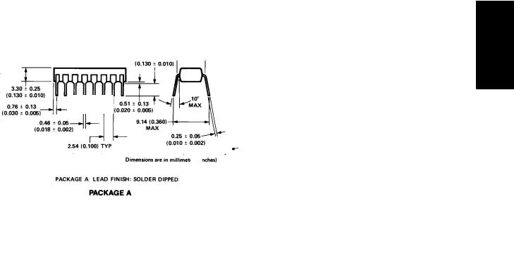
Package Dimensions
25.91 ± 0.25
19.05 ± 0.25 (1.02 ± 0.010)
(0.750 ± 0.010)
15°
1.52 |
± 0.13 |
15° |
|
(0.060 |
± 0.005) |
|
|
|
|
9.40 (0.370) |
|
|
|
|
|
MOTION SENSING AND CONTROL
Operating Characteristics
Table 1. Absolute Maximum Ratings
(All voltages below are referenced to VSS)
Parameter |
Symbol |
Limits |
Units |
|
|
|
|
DC Supply Voltage |
VDD |
-0.3 to +5.5 |
V |
Input Voltage |
VIN |
-0.3 to VDD +0.3 |
V |
Storage Temperature |
TS |
-40 to +125 |
°C |
Operating Temperature |
TA[1] |
-40 to +85 |
°C |
Table 2. Recommended Operating Conditions |
|
||
|
|
|
|
Parameter |
Symbol |
Limits |
Units |
|
|
|
|
DC Supply Voltage |
VDD |
+4.5 to +5.5 |
V |
Ambient Temperature |
T [1] |
-40 to +85 |
°C |
|
A |
|
|
2-179
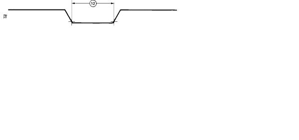
Table 3. DC Characteristics VDD = 5 V ± 5%; TA = -40 to 85°C
Symbol |
Parameter |
|
|
Condition |
Min. |
Typ. |
Max. |
Unit |
|
|
|
|
|
|
|
|
|
|
|
V |
[2] |
Low-Level Input Voltage |
|
|
|
|
|
1.5 |
V |
IL |
|
|
|
|
|
|
|
|
|
V |
[2] |
High-Level Input Voltage |
|
|
|
3.5 |
|
|
V |
IH |
|
|
|
|
|
|
|
|
|
VT+ |
Schmitt-Trigger Positive- |
|
|
|
|
3.5 |
4.0 |
V |
|
|
|
Going Threshold |
|
|
|
|
|
|
|
|
|
|
|
|
|
|
|
|
|
VT- |
Schmitt-Trigger Negative- |
|
|
|
1.0 |
1.5 |
|
V |
|
|
|
Going Threshold |
|
|
|
|
|
|
|
|
|
|
|
|
|
|
|
|
|
VH |
Schmitt-Trigger Hysteresis |
|
|
|
1.0 |
2.0 |
|
V |
|
IIN |
Input Current |
VIN = VSS or VDD |
-10 |
1 |
+10 |
μA |
|||
V |
[2] |
High-Level Output |
I |
OH |
-1.6 mA |
2.4 |
4.5 |
|
V |
OH |
Voltage |
|
|
|
|
|
|
||
|
|
|
|
|
|
|
|
|
|
|
|
|
|
|
|
|
|
|
|
V |
[2] |
Low-Level Output |
I |
OL |
= +4.8 mA |
|
0.2 |
0.4 |
V |
OL |
Voltage |
|
|
|
|
|
|
||
|
|
|
|
|
|
|
|
|
|
|
|
|
|
|
|
|
|||
IOZ |
High-Z Output Leakage |
VO = VSS or VDD |
-10 |
1 |
+10 |
μA |
|||
|
|
Current |
|
|
|
|
|
|
|
|
|
|
|
|
|
|
|||
IDD |
Quiescent Supply Current |
VIN = VSS or VDD, VO = HiZ |
|
1 |
5 |
μA |
|||
C |
IN |
Input Capacitance |
Any Input[3] |
|
5 |
|
pF |
||
|
|
|
|
|
|
|
|
|
|
|
|
|
|
|
|
|
|
||
C |
|
Output Capacitance |
Any Output[3] |
|
6 |
|
pF |
||
OUT |
|
|
|
|
|
|
|
|
|
Notes:
1.Free air.
2.In general, for any VDD between the allowable limits (+4.5 V to +5.5 V), VIL = 0.3 VDD and VIH = 0.7 VDD; typical values are VOH = VDD - 0.5 V @ IOH = -40 μA and VOL = VSS + 0.2 V @ IOL = 1.6 mA.
3.Including package capacitance.
Figure 1. Reset Waveform.
Figure 2. Waveform for Positive Clock Related Delays.
2-180

Functional Pin Description
Table 4. Functional Pin Descriptions
|
|
|
|
|
|
|
|
Pin |
Pin |
|
|
|
|
|
|
|
|
|
Symbol |
2000/2016 |
2020 |
|
|
Description |
|||||||||||
|
|
|
|
|
|
|
|
|
|
|
|
|
|
|
|
|
|
|
|
VDD |
16 |
20 |
Power Supply |
|
|
|
|
|
|
||||||
|
|
VSS |
8 |
10 |
Ground |
|
|
|
|
|
|
||||||
|
CLK |
2 |
2 |
CLK is a Schmitt-trigger input for the external clock signal. |
|||||||||||||
|
|
|
|
|
|
|
|
|
|
|
|
|
|
|
|
|
|
|
CHA |
7 |
9 |
CHA and CHB are Schmitt-trigger inputs which accept the outputs |
|||||||||||||
|
CHB |
6 |
8 |
from a quadrature encoded source, such as incremental optical shaft |
|||||||||||||
|
|
|
|
|
|
|
|
|
|
encoder. Two channels, A and B, nominally 90 degrees out of phase, |
|||||||
|
|
|
|
|
|
|
|
|
|
are required. |
|
|
|
|
|
|
|
|
|
|
|
|
|
|
|
|
|
|
|
|
|
|
|
|
|
|
|
|
5 |
7 |
This active low Schmitt-trigger input clears the internal position |
||||||||||||
|
|
RST |
|
||||||||||||||
|
|
|
|
|
|
|
|
|
|
counter and the position latch. It also resets the inhibit logic. |
RST |
is |
|||||
|
|
|
|
|
|
|
|
|
|
asynchronous with respect to any other input signals. |
|||||||
|
|
|
|
|
|
|
|
|
|
|
|
|
|
|
|
|
|
|
|
|
|
|
|
4 |
4 |
This CMOS active low input enables the tri-state output buffers. The |
|||||||||
|
|
|
OE |
|
|
|
|||||||||||
|
|
|
|
|
|
|
|
|
|
OE and SEL inputs are sampled by the internal inhibit logic on the |
|||||||
|
|
|
|
|
|
|
|
|
|
falling edge of the clock to control the loading of the internal position |
|||||||
|
|
|
|
|
|
|
|
|
|
data latch. |
|
|
|
|
|
|
|
|
|
|
|
|
|
|
|
|
|
|
|
|
|
|
|
|
|
|
|
SEL |
3 |
3 |
This CMOS input directly controls which data byte from the position |
||||||||||||
|
|
|
|
|
|
|
|
|
|
latch is enabled into the 8-bit tri-state output buffer. As in OE above, |
|||||||
|
|
|
|
|
|
|
|
|
|
SEL also controls the internal inhibit logic. |
|||||||
|
|
|
|
|
|
|
|
|
|
|
|
|
|
|
|
|
|
|
|
|
|
|
|
|
|
|
|
|
SEL |
BYTE SELECTED |
|
|
|
||
|
|
|
|
|
|
|
|
|
|
|
|
|
|
|
|
|
|
|
|
|
|
|
|
|
|
|
|
|
0 |
High |
|
|
|
||
|
|
|
|
|
|
|
|
|
|
|
|
|
|
|
|
|
|
|
|
|
|
|
|
|
|
|
|
|
1 |
Low |
|
|
|
||
|
|
|
|
|
|
|
|
|
|
|
|
|
|
|
|
|
|
|
|
|
|
|
|
|
|
|
|
|
|
|
|
|
|
|
|
|
|
|
|
|
|
|
|
|
|
|
|
|
|
|
|
|
|
|
CNTDCDR |
|
16 |
A pulse is presented on this LSTTL-compatible output when the |
|||||||||||||
|
|
|
|
|
|
|
|
|
|
quadrature decoder has detected a state transition. |
|||||||
|
|
|
|
|
|
|
|
|
|
|
|
|
|
|
|
|
|
|
|
|
|
|
|
|
5 |
This LSTTL-compatible output allows the user to determine whether |
|||||||||
|
|
U/D |
|
||||||||||||||
|
|
|
|
|
|
|
|
|
|
the IC is counting up or down and is intended to be used with the |
|
|
|||||
|
|
|
|
|
|
|
|
|
|
CNTDCDR and CNTCAS outputs. The proper signal U (high level) or D |
|||||||
|
|
|
|
|
|
|
|
|
|
(low level) will be present before the rising edge of the CNTDCDR and |
|||||||
|
|
|
|
|
|
|
|
|
|
CNTCAS outputs. |
|
|
|
|
|
|
|
|
CNTCAS |
|
15 |
A pulse is presented on this LSTTL-compatible output when the |
|||||||||||||
|
|
|
|
|
|
|
|
|
|
HCTL-2020 internal counter overflows or underflows. The rising edge |
|||||||
|
|
|
|
|
|
|
|
|
|
on this waveform may be used to trigger an external counter. |
|||||||
|
|
|
|
|
|
|
|
|
|
|
|
|
|
|
|
|
|
|
|
|
D0 |
1 |
1 |
These LSTTL-compatible tri-state outputs form an 8-bit output port |
|||||||||||
|
|
|
|
|
|
|
|
|
|
through which the contents of the 12/16-bit position latch may be read in |
|||||||
|
|
|
D1 |
15 |
19 |
||||||||||||
|
|
|
2 sequential bytes. The high byte, containing bits 8-15, is read first (on the |
||||||||||||||
|
|
|
|
|
|
|
|
|
|
||||||||
|
|
|
D2 |
14 |
18 |
||||||||||||
|
|
|
HCTL-2000, the most significant 4 bits of this byte are set to 0 internally). |
||||||||||||||
|
|
|
D3 |
13 |
17 |
The lower byte, bits 0-7, is read second. |
|||||||||||
|
|
|
|
|
|
|
|
|
|
|
|
|
|
|
|
|
|
|
|
|
D4 |
12 |
14 |
|
|
|
|
|
|
|
|
||||
|
|
|
|
|
|
|
|
|
|
|
|
|
|
|
|
|
|
|
|
|
D5 |
11 |
13 |
|
|
|
|
|
|
|
|
||||
|
|
|
|
|
|
|
|
|
|
|
|
|
|
|
|
|
|
|
|
|
D6 |
10 |
12 |
|
|
|
|
|
|
|
|
||||
|
|
|
|
|
|
|
|
|
|
|
|
|
|
|
|
|
|
|
|
|
D7 |
9 |
11 |
|
|
|
|
|
|
|
|
||||
|
|
|
|
|
|
|
|
|
|
|
|||||||
|
|
|
|
|
|
|
|
|
|
|
|
|
|
|
|
|
|
|
|
NC |
|
6 |
Not connected - this pin should be left floating. |
||||||||||||
|
|
|
|
|
|
|
|
|
|
|
|
|
|
|
|
|
|
MOTION SENSING AND CONTROL
2-181
Switching Characteristics
Table 5. Switching Characteristics Min/Max specifications at VDD = 5.0 ± 5%, TA = -40 to + 85°C.
|
|
|
|
|
|
|
|
Symbol Description |
Min. |
Max. |
Units |
|||||||||||||
|
|
|
|
|
|
|
|
|
|
|
|
|
|
|
|
|
|
|
|
|
|
|
||
1 |
tCLK |
Clock period |
70 |
|
ns |
|||||||||||||||||||
2 |
tCHH |
Pulse width, clock high |
28 |
|
ns |
|||||||||||||||||||
3 |
t |
|
[1] |
Delay time, rising edge of clock to valid, updated count |
|
65 |
ns |
|||||||||||||||||
|
CD |
|
information on D0-7 |
|
|
|
||||||||||||||||||
|
|
|
|
|
|
|
||||||||||||||||||
|
|
|
|
|
|
|
|
|
|
|
|
|
|
|
|
|
|
|
|
|
|
|
||
4 |
tODE |
Delay time, |
|
|
|
|
|
|
|
|
|
|
fall to valid data |
|
65 |
ns |
||||||||
|
OE |
|
||||||||||||||||||||||
|
|
|
|
|
|
|
|
|
|
|
|
|
|
|
|
|
|
|
||||||
5 |
tODZ |
Delay time, |
OE |
|
rise to Hi-Z state on D0-7 |
|
40 |
ns |
||||||||||||||||
6 |
tSDV |
Delay time, SEL valid to stable, selected data byte |
|
65 |
ns |
|||||||||||||||||||
|
|
|
|
(delay to High Byte = delay to Low Byte) |
|
|
|
|||||||||||||||||
|
|
|
|
|
|
|
|
|
|
|
|
|
|
|
|
|
|
|
|
|
|
|
||
7 |
tCLH |
Pulse width, clock low |
28 |
|
ns |
|||||||||||||||||||
8 |
t |
[2] |
Setup time, SEL before clock fall |
20 |
|
ns |
||||||||||||||||||
|
|
SS |
|
|
|
|
|
|
|
|
|
|
|
|
|
|
|
|
|
|
|
|
|
|
|
|
|
|
|
|
|
|
|
|
|
|
|
|
|
|
|||||||||
9 |
t |
[2] |
Setup time, |
OE |
|
before clock fall |
20 |
|
ns |
|||||||||||||||
|
OS |
|
|
|
|
|
|
|
|
|
|
|
|
|
|
|
|
|
|
|
|
|
|
|
10 |
t |
|
[2] |
Hold time, SEL after clock fall |
0 |
|
ns |
|||||||||||||||||
|
SH |
|
|
|
|
|
|
|
|
|
|
|
|
|
|
|
|
|
|
|
|
|
|
|
|
|
|
|
|
|
|
|
|
|
|
|
|
|
|
|
|
||||||||
11 |
tOH[2] |
Hold time, |
OE |
|
|
after clock fall |
0 |
|
ns |
|||||||||||||||
|
|
|
|
|
|
|||||||||||||||||||
12 |
tRST |
Pulse width, |
RST |
low |
28 |
|
ns |
|||||||||||||||||
13 |
tDCD |
Hold time, last position count stable on D0-7 after clock rise |
10 |
|
ns |
|||||||||||||||||||
14 |
tDSD |
Hold time, last data byte stable after next SEL state change |
5 |
|
ns |
|||||||||||||||||||
|
|
|
|
|
|
|
|
|
|
|
|
|
||||||||||||
15 |
tDOD |
Hold time, data byte stable after |
OE |
rise |
5 |
|
ns |
|||||||||||||||||
16 |
tUDD |
|
|
|
|
|
|
|
valid after clock rise |
|
45 |
ns |
||||||||||||
Delay time, U/D |
|
|
||||||||||||||||||||||
17 |
tCHD |
Delay time, CNTDCDR or CNTCAS high after clock rise |
|
45 |
ns |
|||||||||||||||||||
18 |
tCLD |
Delay time, CNTDCDR or CNTCAS low after clock fall |
|
45 |
ns |
|||||||||||||||||||
19 |
tUDH |
|
|
|
|
|
|
|
10 |
|
ns |
|||||||||||||
Hold time, U/D |
stable after clock rise |
|
||||||||||||||||||||||
20 |
tUDCS |
|
|
|
|
|
tCLK-45 |
|
ns |
|||||||||||||||
Setup time, U/D |
valid before CNTDCDR or CNTCAS rise |
|
||||||||||||||||||||||
21 |
tUDCH |
|
|
|
|
|
tCLK-45 |
|
ns |
|||||||||||||||
Hold time, U/D |
stable after CNTDCDR or CNTCAS rise |
|
||||||||||||||||||||||
Notes:
1.tCD specification and waveform assume latch not inhibited.
2.tSS, tOS, tSH, tOH only pertain to proper operation of the inhibit logic. In other cases, such as 8 bit read operations, these setup and hold times do not need to be observed.
Figure 3. Tri-State Output Timing.
2-182

AND CONTROL
MOTION SENSING
Figure 4. Bus Control Timing.
Figure 5. Decoder, Cascade Output Timing (HCTL-2020 only).
2-183
Loading...