


HA12167FB/HA12169FB
Audio Signal Processor for Cassette Deck (Deck 1 Chip)
ADE-207-110B (Z)
3rd. Edition
June 1997
Description
HA12167FB/HA12169FB is silicon monolithic bipolar IC providing REC volume system, Level meter
system and Dolby noise reduction system in one chip.
Functions
• REC equalizer × 2 channel
• Equalizer volume × 2 channel
• Dolby B/C NR × 2 channel
• REC/PB input electronic volume × 2 channel
• Level Meter × 2 channel
• DAC for adjusting bias × 2 channel
Features
• Available to create characteristics of REC equalizer by changing external resistor, no coil
• Equalizer volume is available to calibrate recording automatically with micro-controller
• Electronic volume built-in is available to set the level of recording and play back automatically with
micro-controller
• 4 types of input (3 out of 4 are by way of electronic volume)
• Input electronic control switching is irrelevant to REC/PB electronic control switching
• Dolby noise reduction system is available with double cassette decks (Unprocessed signal output
available from recording out terminals during PB mode)
• Log-compressed level meter output is range from 0 V to 5 V (Usable as music search switchable gain of
0 dB and 20 dB respectively)
• Normal-speed/high-speed, normal/metal/ch rom e fully electronic control switching built-in
• NR-ON/OFF, Dolby B/C, MPX ON/OFF fully electronic control switching built-in
• Reduction of the number of pins by transfered serial data to electronic volume control switching and
another control switching (Controllable from micro-controller directly)
• Small the number of external parts

HA12167FB/HA12169FB
Ordering Information
Operating Voltage
Type Package PB-OUT Level REC-OUT Level Dolby Level Min Max
HA12167FB QFP-80 775 mVrms 300 mVrms 300 mVrms 12.0 V 15.0 V
HA12169FB (14 × 14) 580 mVrms 11.0 V 15.0 V
* Dolby is a trademark of Dolby Laboratories Licensing Corporation.
A license from Dolby Laboratories Licensing Co r por ation is required for the use of this IC.
Rev.3, Jun. 1997, page 2 of 73
HA12167FB/HA12169FB
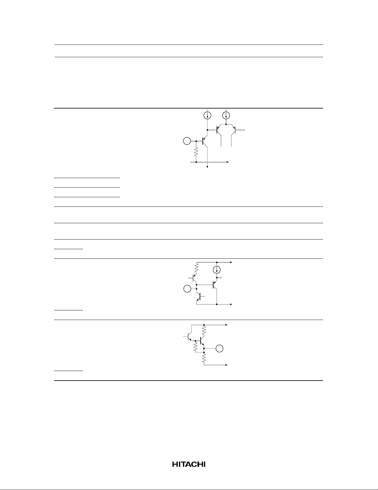
Pin Description (VCC = 14 V, Ta = 25°C, No signal, The value in the show typical value.)
Pin No.
(QFP-80)
65 RPI 100 kΩ V
Terminal
Name Zin DC Voltage Equivalent Circuit Description
/2 Recording input
CC
76
9 LM IN 100 kΩ Level met er input
52
12 EQ IN 100 kΩ Equalizer input
49
66, 67, 69 VRI 100 kΩ VCC/2 + 0.7 V Volume input
72, 74, 75
30, 31 VCC — V
CC
— Power supply
77 REF — VCC/2 — Ripple filter
62 NR IN — VCC/2 NR processor
input
79
3 SS 1 — VCC/2 Spectral skewing
amp input
58
5 CCR — VCC/2 Current controlled
resistor output
56
Rev.3, Jun. 1997, page 3 of 73
HA12167FB/HA12169FB
Pin Description (VCC = 14 V, Ta = 25°C, No signal, The value in the show typical value.)
(Cont)
Pin No.
(QFP-80)
63 IA OUT — V
78
61 VREF Reference voltage
80 buffer output
2 PB OUT Play back
59 (Decode) output
4 SS 2 Spectal skewing
57 amp. output
8 REC OUT Recording
53 (Encode) output
15 EQ OUT Equalizer output
46
1 TP 1.5 kΩ VCC/2
Terminal
Name Zin DC Voltage Equivalent Circuit Description
/2
CC
V
CC
GND
+
–
Input amp output
Bias trap terminal
60
6 HLS DET — 2.3 V Time constant pin
for rectifier
55
7 LLS DET
54
Rev.3, Jun. 1997, page 4 of 73
HA12167FB/HA12169FB
Pin Description (VCC = 14 V, Ta = 25°C, No signal, The value in the show typical value.)
(Cont)
Pin No.
(QFP-80)
64 BIAS — 0.28 V
14 IREF — 1.2 V EQ reference
27 MF EQ parameter
26 fQ current input
25 f/Q
24 GH
23 GL
22 GP
35 BIAS ADJ (N) — 1.2 V Bias DAC
36 BIAS ADJ (M) parameter current
37 BIAS ADJ (C) input
21 HM — —
Terminal
Name Zin DC Voltage Equivalent Circuit Description
Dolby NR
reference current
input
GND
current input
EQ parameter
selector
20 HC
19 HN
18 NM
17 NC
16 NN
GND
Rev.3, Jun. 1997, page 5 of 73
HA12167FB/HA12169FB
Pin Description (VCC = 14 V, Ta = 25°C, No signal, The value in the show typical value.)
(Cont)
Pin No.
(QFP-80)
68 CONT 3.3 kΩ V
Terminal
Name Zin DC Voltage Equivalent Circuit Description
/2 – 1.5 V
CC
to V
CC
V /2
CC
/2
DAC output
volume control
input
DAC
OUT
73
13 EQ CONT 1.65 kΩ
48
10 LM DET — 0.2 V
LM
Time constant pin
for level meter
OUT
GND
LM DET
51
11 LM OUT — 0.2 V Level meter output
50
45 NR ON/OFF 100 kΩ —
Mode control time
constant
44 C/B
43 MPX
Rev.3, Jun. 1997, page 6 of 73
GND
HA12167FB/HA12169FB
Pin Description (VCC = 14 V, Ta = 25°C, No signal, The value in the show typical value.)
(Cont)
Pin No.
(QFP-80)
42 RESET 100 kΩ —
41 STB
40 DATA
39 CLK
38 INJ — 0.7 V — Injection current
47 D-GND — 0.0 V — Digital (Logic)
70 GND — 0.0 V — Ground
71, 34
28 BIAS CONT — —
Terminal
Name Zin DC Voltage Equivalent Circuit Description
Mode control input
D•GND
GND
2
L
input I
ground
V
CC
Bias DAC output
33
29 DAC OUT — —
32
GND
V
CC
GND
Rev.3, Jun. 1997, page 7 of 73
Bias DAC buffer
out
HA12167FB/HA12169FB
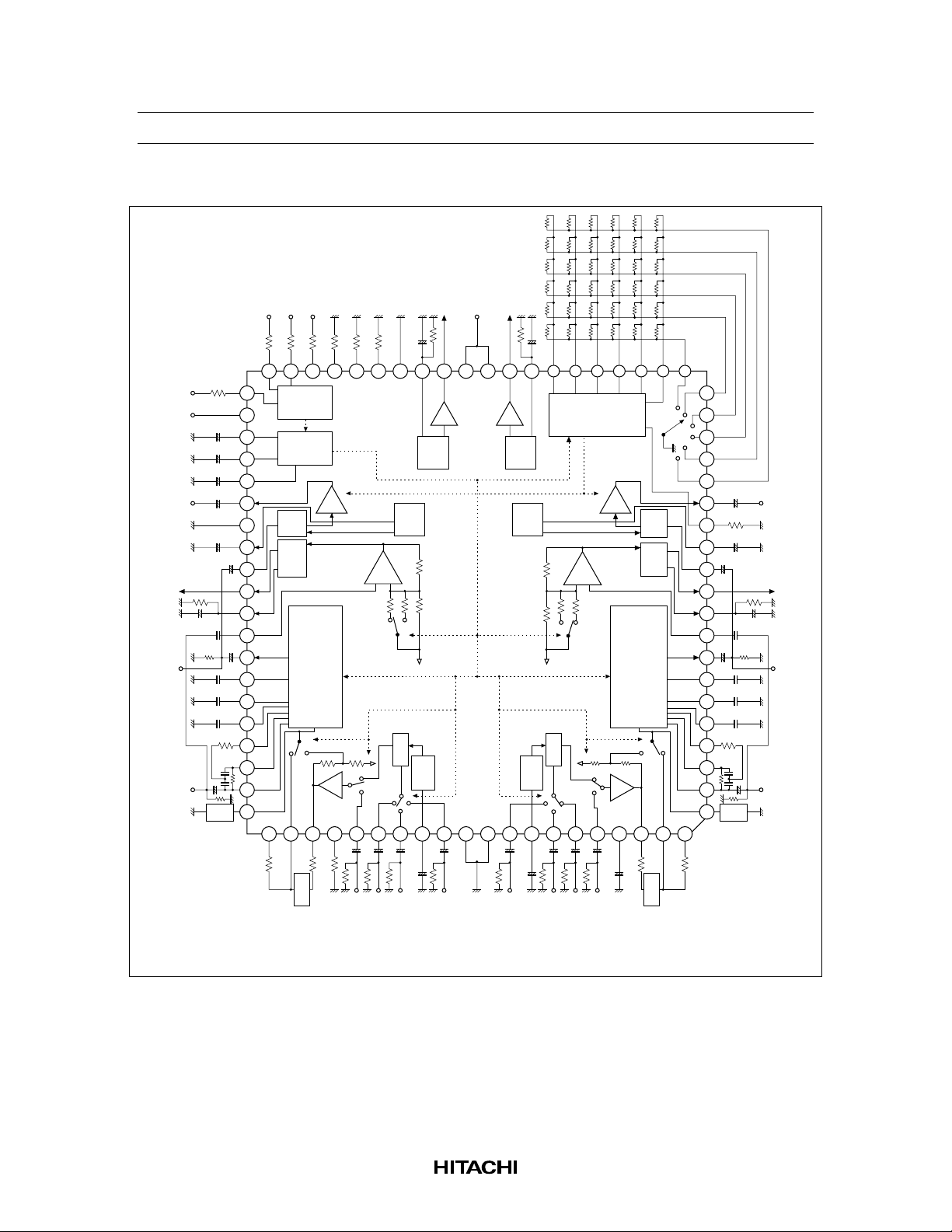
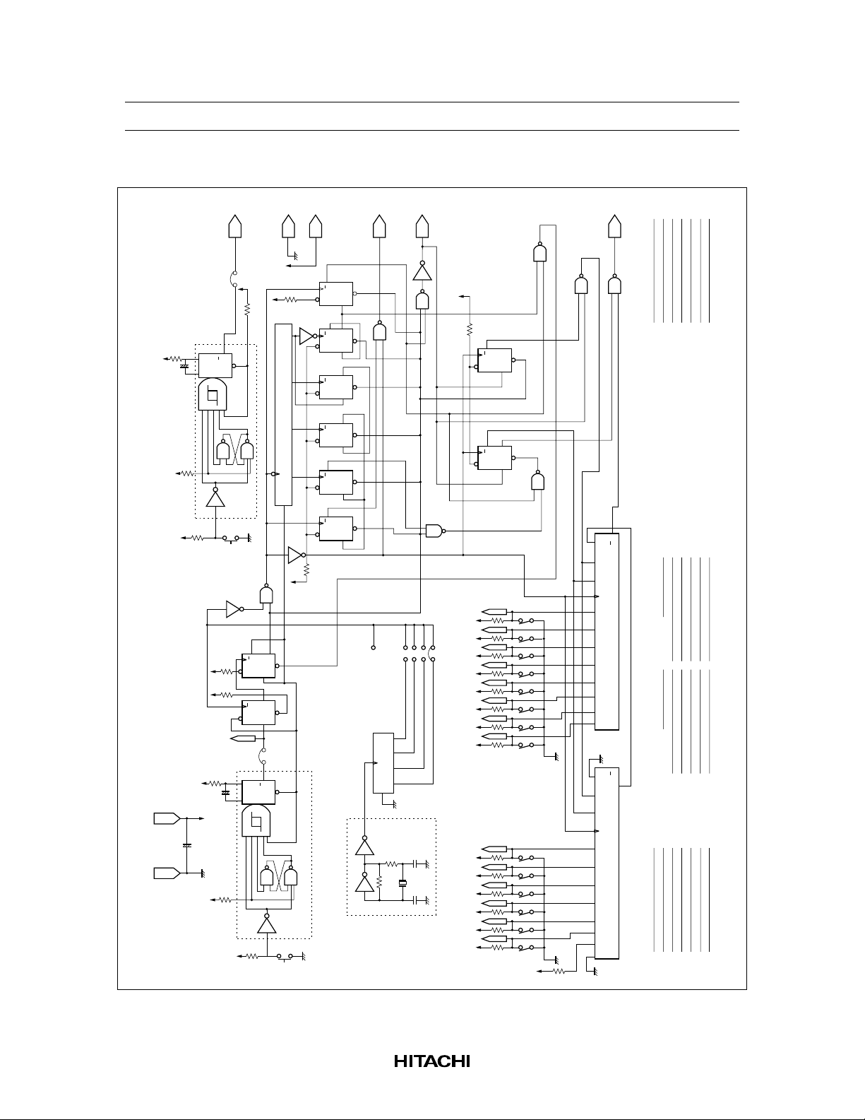
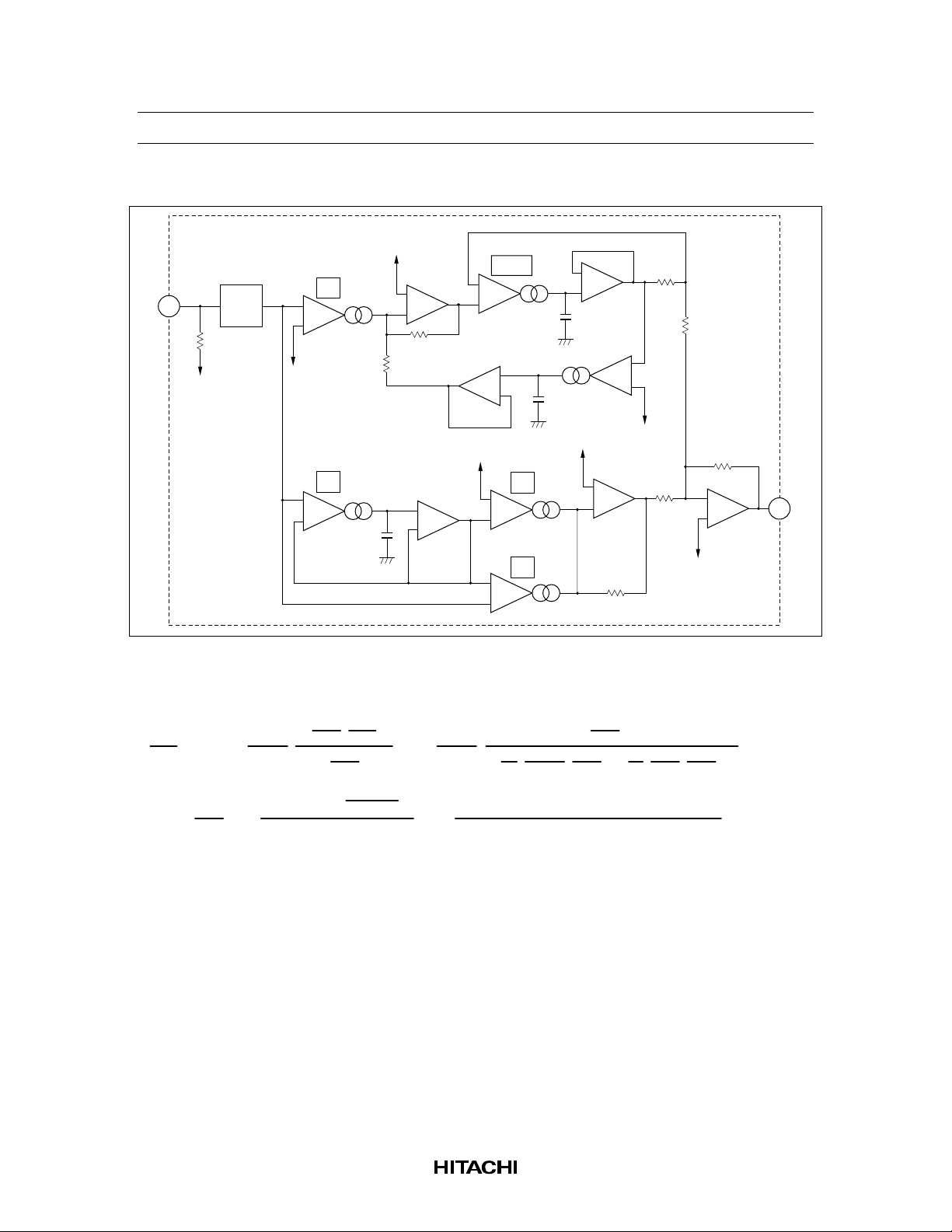
Block Diagram
DATA
CLK
INJ
BIAS ADJ (C)
BIAS ADJ (M)
40
39
38
37
36
STB
RESET
IIL
LOGIC
BIAS ADJ (N)
GND
35
34
BIAS CONT (L)
DAC OUT (L)
33
32
31
CC
V
30
29
DAC OUT (R)
BIAS CONT (R)
FMfQf/QGHGLGPHM
28
27
26
25
24
23
22
EQ-CONTROLER
21
2019181716151413121110987654321
EQ
EQ
LM
LM
LM
REC
LLS
HLS
NR
ON/
(L)
OUT
(L)
CONT
(L)
OUT
(L)
DET
IN
(L)
(L)
OUT
(L)
DET
(L)
DET
(L)
CCR
(L)
SS2
PBOUT
TP
C/B MPX
OFF
D-GND
EQ
SS1
(L)
(L)
SW
6BIT
DAC
6BIT
DAC
NN NC NM HN HC
(R)
EQ
TRAP
IN
SS1
(R)
(R)
IREF
EQ
OUT
EQ
CONT
LM
OUT
LM
DET
IN
LM
REC
OUT
LLS
DET
HLS
DET
(R)
CCR
(R)
SS2
(R)
PBOUT
TP
(R)
(R)
(R)
(R)
(R)
(R)
(R)
(R)
EQ
REC
DAC
EQ
VOL
IN
(L)
RECT
5BIT
LMA
–
+
5BIT
DAC
DOLBY B/C NR
(L)
IA
TRAP
BIAS
60 59 58 57 56 55 54 53 52 51 50 49 48 47 46 45 44 43 42 41
61
62
63
64
E. VOL
DAC
6BIT
65
66
67
68
69
70
71
E. VOL
DAC
6BIT
72
73
74
MPX
EQ
REC
EQ
VOL
LMA
–
+
RECT
DOLBY B/C NR
IA
BIAS
75
76
77
78
79
80
MPX
Vref (L)
NRIN (L)
IA OUT (L)
Rev.3, Jun. 1997, page 8 of 73
BIAS
RPI (L)
VRI 3 (L)
VRI 2 (L)
VRI 1 (L)
CONT (L)
GND
VRI 1 (R)
CONT (R)
VRI 2 (R)
VRI 3 (R)
RPI (R)
REF
NRIN (R)
IA OUT (R)
Vref (R)
HA12167FB/HA12169FB
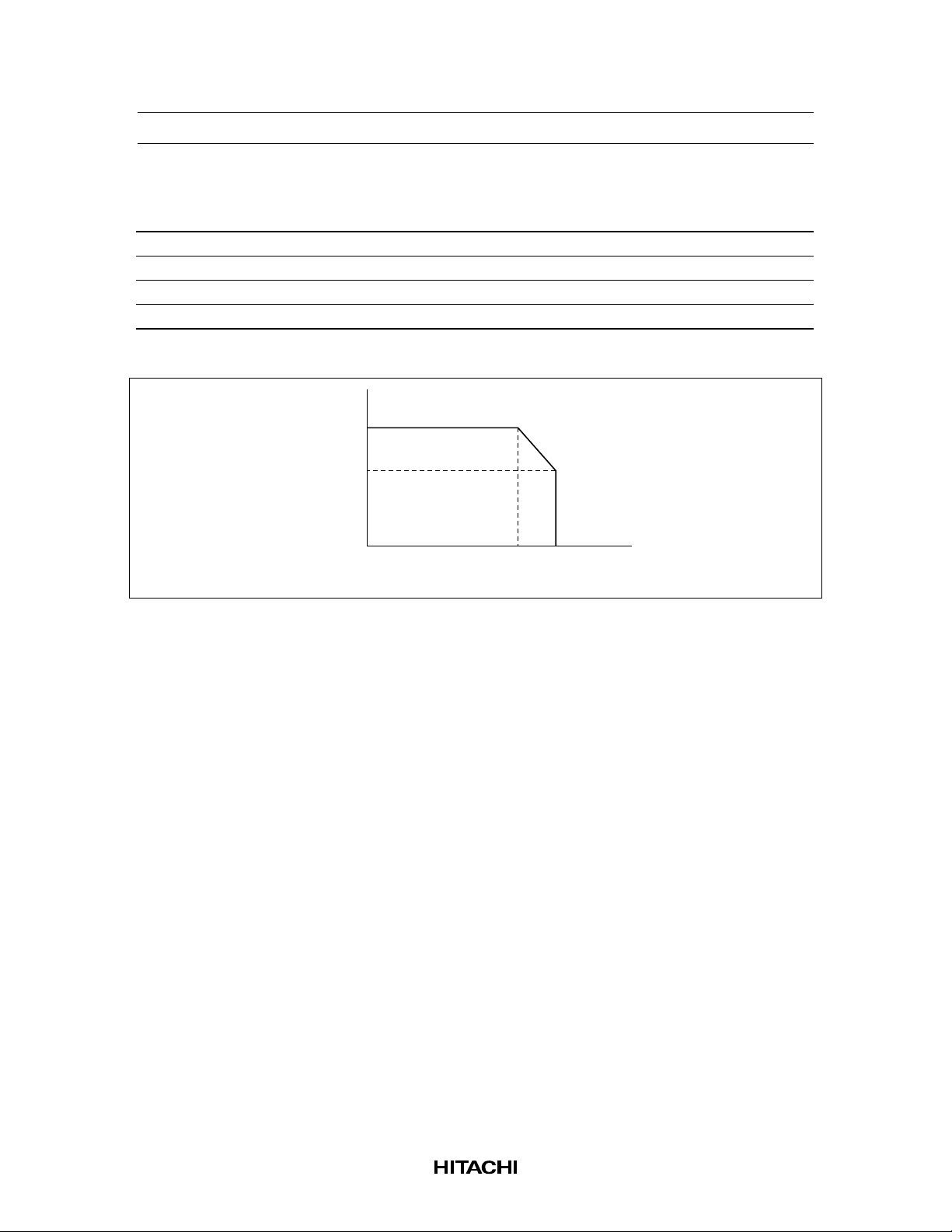
Absolute Maximum Ratings
Item Symbol Rating Unit Note
Supply voltage V
Power dissipation Pd 750 mW 1
Operating temperature Topr –30 to +75 °C
Storage temperature Tstg –55 to +125 °C
Note: For Ta is higher than 65°C, reduce Pd at the rate of 12.5 mW/°C.
Please, see the below graph.
max 15 V
CC
[mW]
750
625
Pd
–30 65 75
Ta [˚C]
Rev.3, Jun. 1997, page 9 of 73

HA12167FB/HA12169FB
Electrical Characteristics (Ta = 25°C, VCC = 14 V, Dolby Level 300 mVrms at
RECOUT)
Application Terminal
—————————
Input Output
———– ———–
R L R L Note
————303176 65 78 63
76 65 8 53
76 65 8 53
76 65 8 53
76 65 8 53
76 65 8 53
76 65 8 53 1
76 65 8 53
76 65 8 53
72 69 8 53
72/ 69/ 2 59
74 67
72/ 69/ 2 59
76 65
Tape DAC DAC DAC [Hz] Level
Meter Speed
ON
ON
ON
ON
→
→
→
Test Conditions
—————————————————————————————————————
REC RV Input Tape Input EQ Bias fin OUT
Specification REC
——————–
IA 18.5 20.0 21.5 dB REC RV ON OFF B RPI NOR NOR NOR 63 0 0 1 k 0
V
IQ — 34.5 42.0 mA PB PV OFF OFF B VRI1 NOR NOR NOR 32 0 0 ——No signal
G
RPI
——————————————————————————————————————————————————————————————————–
Quiescent
current
———————————————————————————————————————————————————————————
Input amp.
Item Symbol Min Typ Max Unit /PB /PV MPX NR B/C Pin
gain
———————————————————————————————————————————–
B-ENC 2.8 4.3 5.8 dB REC RV ON OFF B RPI NOR NOR NOR 63 0 0 2 k –20
-2 k
————————–
B-ENC 1.7 3.2 4.7 REC RV ON OFF B RPI NOR NOR NOR 63 0 0 5 k –20
-5 k
———————————————————————————————————————————————————————————
B-type
encode
boost
———————————————————————————————————————————–
C-ENC 3.9 5.9 7.9 dB REC RV ON OFF C RPI NOR NOR NOR 63 0 0 1 k –20
-1 k (1)
————————–
C-ENC 18.1 19.6 21.6 REC RV ON OFF C RPI NOR NOR NOR 63 0 0 1 k –60
———————————————————————————————————————————————————————————
C-typ
encode
boost
ON
→
→
———————————————————————————————————————————–
Max 12.0 13.0 — dB REC RV ON ON C RPI NOR NOR NOR 63 0 0 1 k —
-1 k (2)
————————–
O
C-ENC 9.8 11.8 13.8 REC RV ON OFF C RPI NOR NOR NOR 63 0 0 700 –30
-700
V
———————————————————————————————————————————————————————————
ratio CCIR/ARM
Signal handling
———————————————————————————————————————————————————————————
Signal to noise S/N (C) 60.0 63.0 — dB REC RV ON ON C RPI NOR NOR NOR 63 0 0 ——Rg = 5.1 kΩ
———————————————————————————————————————————————————————————
T.H.D. THD (C) — 0.08 0.3 % REC RV ON ON C RPI NOR NOR NOR 63 0 0 1 k 0
———————————————————————————————————————————————————————————
Crosstalk CT —–85.0 –79.0 dB REC RV ON OFF B VPI1 NOR NOR NOR 0 0 0 1 k 6
←→
———————————————————————————————————————————–
L)
←→
(R
(VRI1
————————–
CT —–80.0 –74.0 REC RV ON OFF B VRI1 NOR NOR NOR 0 0 0 1 k 6
←→
———————————————————————————————————————————–
VRI2) VRI2
←→
RPI) RRI
←→
(VRI1
————————–
CT —–80.0 –74.0 REC RV ON OFF B VRI1 NOR NOR NOR 0/63 0 0 1 k 6
———————————————————————————————————————————————————————————
Rev.3, Jun. 1997, page 10 of 73

HA12167FB/HA12169FB
Electrical Characteristics (Ta = 25°C, VCC = 14 V, Dolby Level 300 mVrms at
RECOUT) (Cont)
Application Terminal
—————————
Input Output
———– ———–
R L R L Note
————3940————41
76 65 2 59
——259 2
76 65 78 63
72 69 78 63
72 69 78 63
72 69 78 63
72 69 78 63
72 69 2 59
72 69 2 59
72 69 2 59 3
72 69 2 59 3
STB
Tape DAC DAC DAC [Hz] Level
Meter Speed
Test Conditions
—————————————————————————————————————
REC RV Input Tape Input EQ Bias fin OUT
High
Low
HA12169
HA12167
REC RV ON OFF B RPI NOR NOR NOR 63 0 0 1 k 0
mVrms
ON
→
Rg = 5.1 k, A-WTG
Specification REC
——————–
H4.0— 5.3 V ——————————————CLK, DATA,
L –0.2 — 1.0 ——————————————
S
S
V
17.5 19.1 21.5 dB REC RV ON OFF B VRI1 NOR NOR NOR 0 0 0 1 k — Vin = 100 mVrms
–56.0 –50.0 –47.0 dB REC RV ON OFF B VRI1 NOR NOR NOR 62 0 0 1 k — Vin = 2 Vrms
27.0 29.0 31.0 dB PB PV ON OFF B VRI1 NOR NOR NOR 0 0 0 1 k — Vin = 100 mVrms
15.0 17.0 19.0 dB PB PV ON OFF B VRI1 NOR NOR NOR 62 0 0 1 k — Vin = 100 mVrms
—–82 –75 dB REC RV ON OFF B VRI1 NOR NOR NOR 63 0 0 1 k — Vin = 2 Vrms
11.0 12.0 — dBS REC RV ON OFF B VRI1 NOR NOR NOR 42 0 0 1 k — THD = 1%
78.0 84.0 — dB REC RV ON OFF B VRI1 NOR NOR NOR — 0 0 (1 k) 0 Vin = 100 mVrms
VR
rec VR
rec VR
V
∆Gv –1.0 0.0 1.0 dB ——————————————
V
G
——————————————————————————————————————————————————————
G
(Max)
(Min)
VR
V PB
V PB
G
——————————————————————————————————————————————————————
G
(Max)
(Min)
CTrec VR
(MUT)
S/N (VR)
— 0.04 0.3 % REC RV ON OFF B VRI1 NOR NOR NOR — 0 0 1 k 0 Vin = 100 mVrms
THD (VR)
—————————— ———————————————————————————– ——————–
——– —————–
——————————————————————————————————————————————————————————————————–
Serial digital V
———————————————————————————————————————————————————————————
PB- Vout 500 580 670
level 665 775 900
———————————————————————————————————————————————————————————
PB-out of fset Vofs –100 0.0 +100 mV PB PV OFF OFF C RPI NOR NOR NOR 63 0 0 ——No signal
———————————————————————————————————————————————————————————
Channel balance
———————————————————————————————————————————————————————————
REC volume
Item Symbol Min Typ Max Unit /PB /PV MPX NR B/C Pin
input level
output
gain
———————————————————————————————————————————————————————————
PB volume gain
———————————————————————————————————————————————————————————
REC volume
mute level
———————————————————————————————————————————————————————————
REC volume max Vin max
———————————————————————————————————————————————————————————
Signal to noise
volume
———————————————————————————————————————————————————————————
T.H.D. of REC
input level (VR)
ratio of REC
———————————————————————————————————————————————————————————
volume
Rev.3, Jun. 1997, page 11 of 73

HA12167FB/HA12169FB
Electrical Characteristics (Ta = 25°C, VCC = 14 V, Dolby Level 300 mVrms at
RECOUT) (Cont)
Application Terminal
—————————
Input Output
———– ———–
R L R L Note
12 49 15 46
12 49 15 46
12 49 15 46
12 49 15 46
12 49 15 46
12 49 15 46
12 49 15 46
12 49 15 46
12 49 15 46
——15 46 4
9521150
9521150
9521150
A-WTG
9521150
Tape DAC DAC DAC [Hz] Level
Meter Speed
Test Conditions
—————————————————————————————————————
REC RV Input Tape Input EQ Bias fin OUT
Specification REC
——————–
Item Symbol Min Typ Max Unit /PB /PV MPX NR B/C Pin
———————————————————————————————————————————–
———————————————————————————————————————————–
———————————————————————————————————————————–
57.0 62.0 — dB REC RV ON OFF B RPI NOR NOR NOR 63 0 0 ——Rg = 5.1 kΩ,
— 0.2 0.5 % REC RV ON OFF B RPI NOR NOR NOR 63 16 0 1 k — Vin = –26 dBs
–400 0.0 +400 mV REC RV OFF OFF B RPI NOR NOR NOR 63 0 0 ——No signal
EQ 23.5 25.5 27.5 dB REC RV ON OFF B RPI NOR NOR NOR 63 0 0 500 — Vin = –32 dBs
EQ 23.5 25.5 27.5 REC RV ON OFF B RPI NOR NOR NOR 63 0 0 1 k — Vin = –32 dBs
V
(500)
————————–
——————————————————————————————————————————————————————————————————–
Equalizer gain G
EQ 25.0 27.0 29.0 REC RV ON OFF B RPI NOR NOR NOR 63 0 0 5 k — Vin = –32 dBs
V
V
(1 k)
G
(5 k)
————————–
G
————————–
EQ 6 8 10 dB REC RV ON OFF B RPI NOR NOR NOR 63 0/30 0 1 k — Vin = –32 dBs
EQ 31.0 33.5 36.0 REC RV ON OFF B RPI NOR NOR NOR 63 0 0 12 k — Vin = –32 dBs
V
V
(12 k)
G
∆G
(1 k)
———————————————————————————————————————————————————————————
Equalizer volume
variable a range
———————————————————————————————————————————————————————————
EQ —–75 –62 dB REC RV ON OFF B RPI NOR NOR NOR 63 31 0 1 k — Vin = –9 dBs
V
G
S/N (EQ)
THD (EQ)
Equalizer max Vin Max –10.0 –9.0 — dBS REC RV ON OFF B RPI NOR NOR NOR 63 16 0 1 k — THD = 1%
mute gain (MUT) 1 kHz BPF
input level (EQ)
———————————————————————————————————————————————————————————
Equalizer volume
———————————————————————————————————————————————————————————
Signal to noise
radio of equalizer
———————————————————————————————————————————————————————————
THD of equalizer
———————————————————————————————————————————————————————————
Equalizer of fset Vofs (EQ)
———————————————————————————————————————————————————————————
Level meter LM 2.50 2.75 3.00 V REC RV ON OFF B RPI NOR NOR NOR 63 0 0 1 k 0
1
2
——————————————————————————————————————————————————————
LM 3.55 3.85 4.15 V REC RV ON OFF B RPI NOR NOR NOR 63 0 0 1 k 12
(12 dB)
——————————————————————————————————————————————————————
LM 0.70 1.00 1.30 V REC RV ON OFF B RPI NOR NOR NOR 63 0 0 1 k –20
(–20 dB)
——————————————————————————————————————————————————————
LM 2.45 2.75 3.05 V REC RV ON OFF B RPI 20 dB NOR NOR 63 0 0 1 k –20
(–20 dB)
output (0 dB)
———————————————————————————————————————————————————————————
Rev.3, Jun. 1997, page 12 of 73

HA12167FB/HA12169FB
Electrical Characteristics (Ta = 25°C, VCC = 14 V, Dolby Level 300 mVrms at
RECOUT) (Cont)
Application Terminal
—————————
Input Output
———– ———–
R L R L Note
——11 50
——11 50
——29 32
——29 32
Tape DAC DAC DAC [Hz] Level
Meter Speed
Test Conditions
—————————————————————————————————————
REC RV Input Tape Input EQ Bias fin OUT
Specification REC
——————–
———————————————————————————————————————————–
= 11 V
= 12 V
CC
CC
Max 11.0 12.0 13.0 V REC RV OFF OFF B VRI1 NOR NOR MET 63 0 63 ——
Min — 0.5 1.0 V REC RV OFF OFF B VRI1 NOR NOR MET 63 0 0 ——
B
LMofs 1 — 150 300 mV REC RV ON OFF B RPI NOR NOR NOR 63 0 0 ——No signal
————————–
LMofs 2 — 200 350 REC RV ON OFF B RPI 20 dBNOR NOR 63 0 0 ——No signal
——————————————————————————————————————————————————————————————————–
Level meter of
fset
Item Symbol Min Typ Max Unit /PB /PV MPX NR B/C Pin
B
V
V
———————————————————————————————————————————————————————————
DAC output Max
———————————————————————————————————————————————————————————
DAC output Min
= 15 V
= 15 V
CC
CC
HA12169: V
3. Adjust the input volume to Dolby level.
4. V
2. V
——————————————————————————————————————————————————————————————————–
Note: 1. HA12167: V
Rev.3, Jun. 1997, page 13 of 73
HA12167FB/HA12169FB
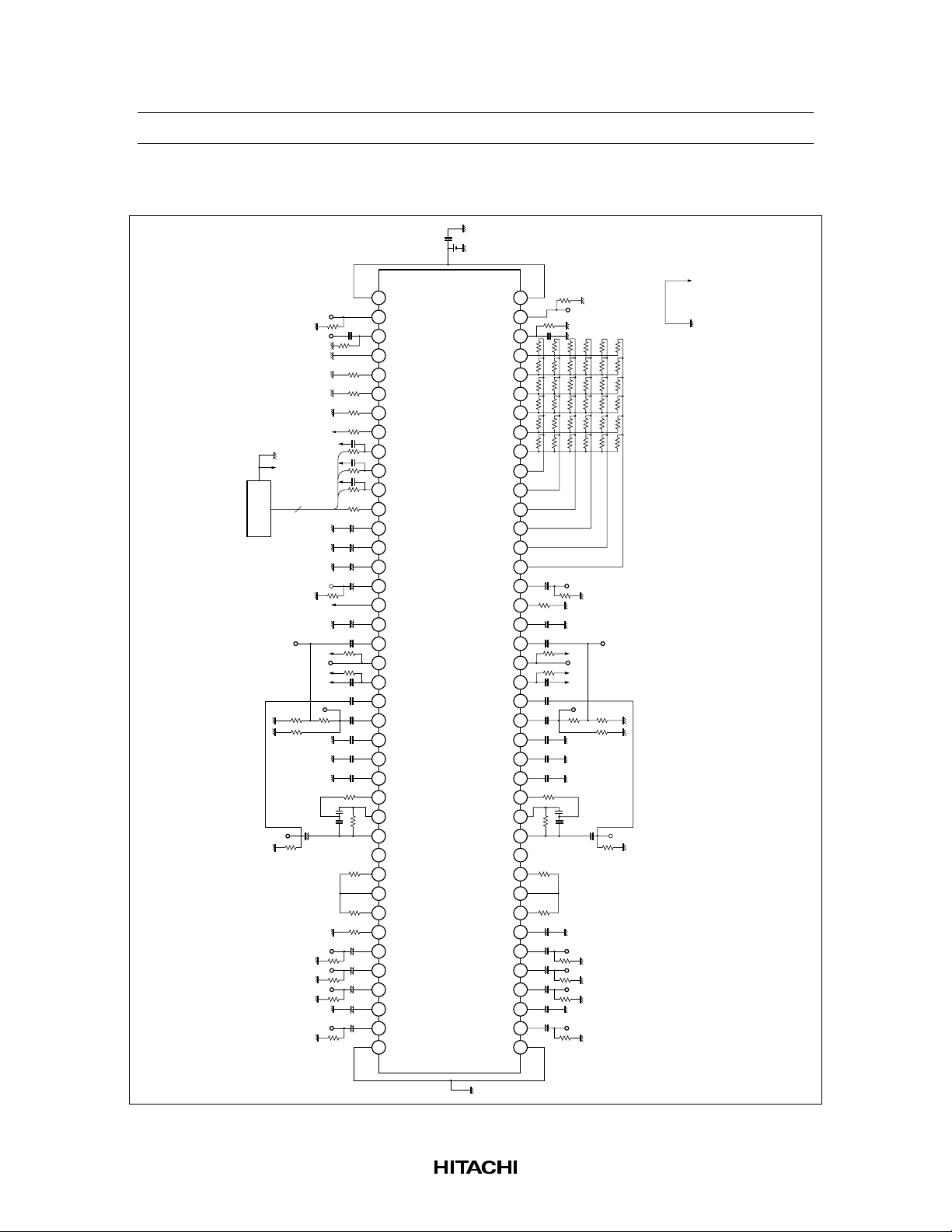
Test Circuit
C41
100µ
+
CC
V
MODE
CONTROLLER
CC
V
10k
R12
1µ
C14
+
R13
100k
35 34 33 32 31
33k
R14
36
20k
R15
37
24k
R16
+5V
C45C46C47
4
10k
R21
GND
Digital
51k
R22
R23
100k
1µ
C21
47k
R25
R24
7.5k
12k
R79
C29
2.2µ
2200p 2200p
+
10k
R28
38
R17
1.2k
10P10P10P
22k
R18
40 39
22k
R19
41
22k
R20
22k
R80
+++
C15
4.7µ
44 43 42
C16
4.7µ
45
C17
4.7µ
46
+
C18
2.2µ
47
48
++
1µ
C19
C20
0.47µ
49
51 50
+
C22
0.1µ
52
+
C23
2.2µ
C24
0.1µ
C25
0.1µ
56 55 54 53
C26
2200p
57
560
R26
C27 C28
22k
R27
59 58
60
R29
5.6k
62 61
DAC OUT(L)
BIAS CONT(L)
GND
BIAS ADJ(N)
BIAS ADJ(M)
BIAS ADJ(C)
INJ
CLK
DATA
STB
RESET
MPX
C/B
NR ON/OFF
EQOUT(L)
DGND
EQCONT(L)
EQIN(L)
LMOUT(L)
LMDET(L)
LMIN(L)
RECOUT(L)
LLSDET(L)
HLSDET(L)
CCR(L)
SS2(L)
SS1(L)
PB OUT(L)
TP(L)
Vref(L)
NR IN(L)
HA12167/HA12169 (REC 1 CHIP)
IAOUT(L)
R30
2.4k
18k
R31
+++
C30
R32
5.1k
C31
10k
R33
C32
10k
R34
++
C33
C34
R35
5.1k
0.47µ
0.47µ
0.47µ
1µ
0.47µ
BIAS
64 63
RPI(L)
65
VRI3(L)
VRI2(L)
CONT(L)
VRI1(L)
GND
70 69 68 67 66
CC
V
DAC OUT(R)
BIAS CONT(R)
FM
fQ
f/Q
GH
GL
GP
HM
HC
NH
NM
NC
NN
EQOUT(R)
IREF
EQCONT(R)
EQIN(R)
LMOUT(R)
LMDET(R)
LMIN(R)
RECOUT(R)
LLSDET(R)
HLSDET(R)
CCR(R)
SS2(R)
SS1(R)
PB OUT(R)
TP(R)
Vref(R)
NR IN(R)
IAOUT(R)
REF
RPI(R)
VRI3(R)
VRI2(R)
CONT(R)
VRI1(R)
GND
R11
30
29
28
+
R54R55R56R57R58R59
R48R49R50R51R52R53
27
26
25
24
23
R47 R46 R45 R44 R43 R42
22
21
20
19
18
17161514
C12
2.2µ
+
1µ
C11
13
+
C10
0.47µ
12
11
10
++
9
C8
0.1µ
8
+
C7
2.2µ
7
C6
0.1µ
654
C5
0.1µ
C4
2200p
R3
560
3
C2 C3
R2
22k
2
1
80
R41
5.6k
79
787372
R40
2.4k
C39
76 77
75
74
+
C37 C38 C39 C40
0.47µ 0.47µ 0.47µ 1µ
+++++
1µ
C36
C35
0.47µ
71
R36
10k
2200p 2200p
R10
100k
1µ
C13
R60R61R62R63R64R65
R66R67R68R69R70R71
R72R73R74R75R76R77
33k 33k 33k 51k 51k 100k
R9
10k
R8
24k
R7
51k
R6
100k
1µ
C9
R5
7.5k
R4
47k
12k
R78
C1
2.2µ
+
R1
10k
R39
5.1k
10k
R38
10k
R37
5.1k
AGND DGND
Rev.3, Jun. 1997, page 14 of 73
Mode Controller
HA12167FB/HA12169FB
R8
C2
GND VCC(+5V)
N7 IC10
.IN
Serial
LOAD
SHIFT
CLK
INHI
CLK
BCD E F G H
A
.IN
Serial
LOAD
SHIFT
CLK
INHI
CLK
ABCD E F G H
DATA
2
H
Q
BIT
Q
HH
Q
BIT
Pin Name
RST
DATA
Output connector CN1
Pin No.123456
CN3MNZGND
Pin Name
CN2EFGH
D10 IC8D11 IC9
Pin No.5678
CN3IJKL
Pin Name
CN2ABCD
Pin No.1234
TTL Type
74HC221
74HC00
IC No.12, 10
CLK
STB
74HC74
74HC393
3, 5, 6, 7, 1248, 9
VCC
GND
74HC165
74HC04
11
VCC
1 RST
JP1
1M
Q
Q
+
2.2µ
R7
+
CLR
22k
R6
22k
SW16
N8 IC11
R5
22k
R9
22k
Z
R3
1M
+
C1
2.2µ
C3
100µ
R2
22k
6GND
5
D3 IC12
Q
R27
22k
D10
IC11
ABCD
QQQQ
CLR
D15 IC12 D7 IC5 D6 IC5 D5 IC6
N9 IC11
R26
22k
D2 IC3
D1 IC3
TRIGGER
IC 1
SW15
PR
D4 IC6
Q
PR
Q
PR
Q
PR
Q
PR
Q
PR
R29
22k
D13 IC4
IC1
N1 IC2
Q
Q
CLR
PR
D
Q
Q
CLR
PR
D
JP2
Q
Q
CLR
R1
22k
Q
CLR
D
Q
CLR
D
Q
CLR
D
Q
CLR
D
Q
CLR
D
Q
CLR
D
N12 IC11 N13 IC11
X'tal OSC
N2 IC2
MCLK
D12 IC4
CLK
STB
3
CLR
R9
ABCD
QQ QQ
R10
1M
SW17
510
X'tal
125kHz
62.5kHz
N11 IC11N3 IC2
C5
120P
1MHz
4
250kHz
C4
30P
N5 IC10
500kHz
N4 IC2
N6 IC10
R28
22k
D4 IC7
Q
Q
CLR
PR
D
Q
Q
CLR
PR
D
D9
IC7
A
R24
22k
B
R23
22k
C
R22
22k
D
R21
22k
EFGH
R20
22k
R19
22k
R18
22k
R17
22k
I
R16
22k
J
R15
22k
K
R14
22k
L
R13
22k
M
R12
22k
N
R11
22k
N8 IC10
SW1SW2SW3SW4SW5SW6SW7SW8
SW9
SW10SW11SW12SW13SW14
R25
22k
Rev.3, Jun. 1997, page 15 of 73
HA12167FB/HA12169FB
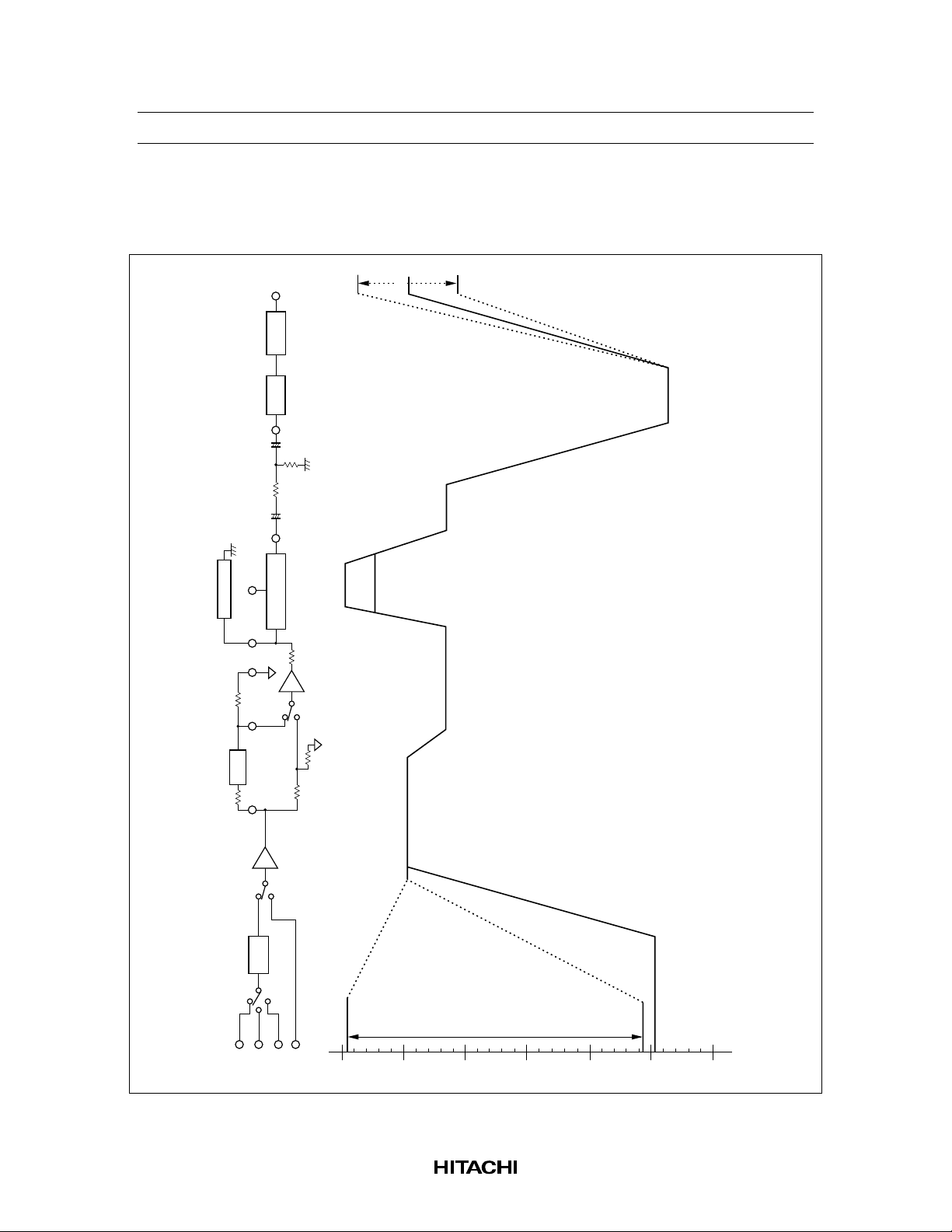
Level Diagram
REC Mode (1 kHz NR-OFF)
EQOUT
EQIN
RECOUT
PBOUT
BIAS TRAP
TP
5.6k
E. VOL REC EQ
+
+
DOLBY - NR
1.5k
–1dBs
775mVrms
0dBs
HA12167
580mVrms
–2.5dBs
HA12169
–5dBs
–9dBs
–26dBs
0dBs = 775mVrms
–8.2dBs
300mVrms
–8.2dBs
* Input limit of VRI is more than 12dB on Vo max, and not variable range.
2.4k
MPX
VRI 1
NRIN VREF
IAOUT
IA
E. VOL
VRI 2
VRI 3
14k
6k
RPI
Rev.3, Jun. 1997, page 16 of 73
–0.4dBs
0
–5.2dBs
–5
43mVrms
–25.2dBsRPI
–24.3
VRI*
–10
–15
dBs
–20
–25
–30
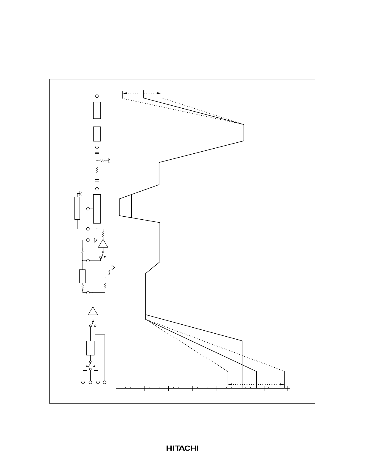
PB Mode (1 kHz NR-OFF)
HA12167FB/HA12169FB
EQOUT
EQIN
RECOUT
PBOUT
BIAS TRAP
TP
5.6k
E. VOL REC EQ
+
+
DOLBY - NR
1.5k
–1dBs
775mVrms
0dBs
(HA12167)
–5dBs
580mVrms
–2.5dBs
(HA12169)
–8.2dBs
–8.2dBs
–9dBs
300mVrms
0dBs = 775mVrms
–26dBs
2.4k
MPX
VRI 1
NRIN VREF
IAOUT
IA
E. VOL
VRI 2
VRI 3
RPI
14k
6k
–5.2dBs
–25.2
dBs
43mVrms
RPI
–28.2
–22.2dBs
0
–5
–10
–15
–20
dBs
–25
VRI
–34.2
dBs
–30
–35
Rev.3, Jun. 1997, page 17 of 73
HA12167FB/HA12169FB
Application Note
Power Supply Range
HA12167FB/HA12169FB are designed to operate on either single supply or split supply.
The operating range of the supply voltage is shown in table 1.
Table 1 Supply Voltage
Type No. Single Supply Split Supply
HA12167FB 12 V to 15 V ±6.0 V to 7.5 V
HA12169FB 11 V to 15 V ±6.0 V to 7.5 V
The lower limit of supply voltage depends on the line output reference level.
The minimum value of the overload margin is specified as 12 dB by Dolby Laboratories. HA12167 series
are provided with two line output level, which will permit an optimum overload margin for power supply
conditions.
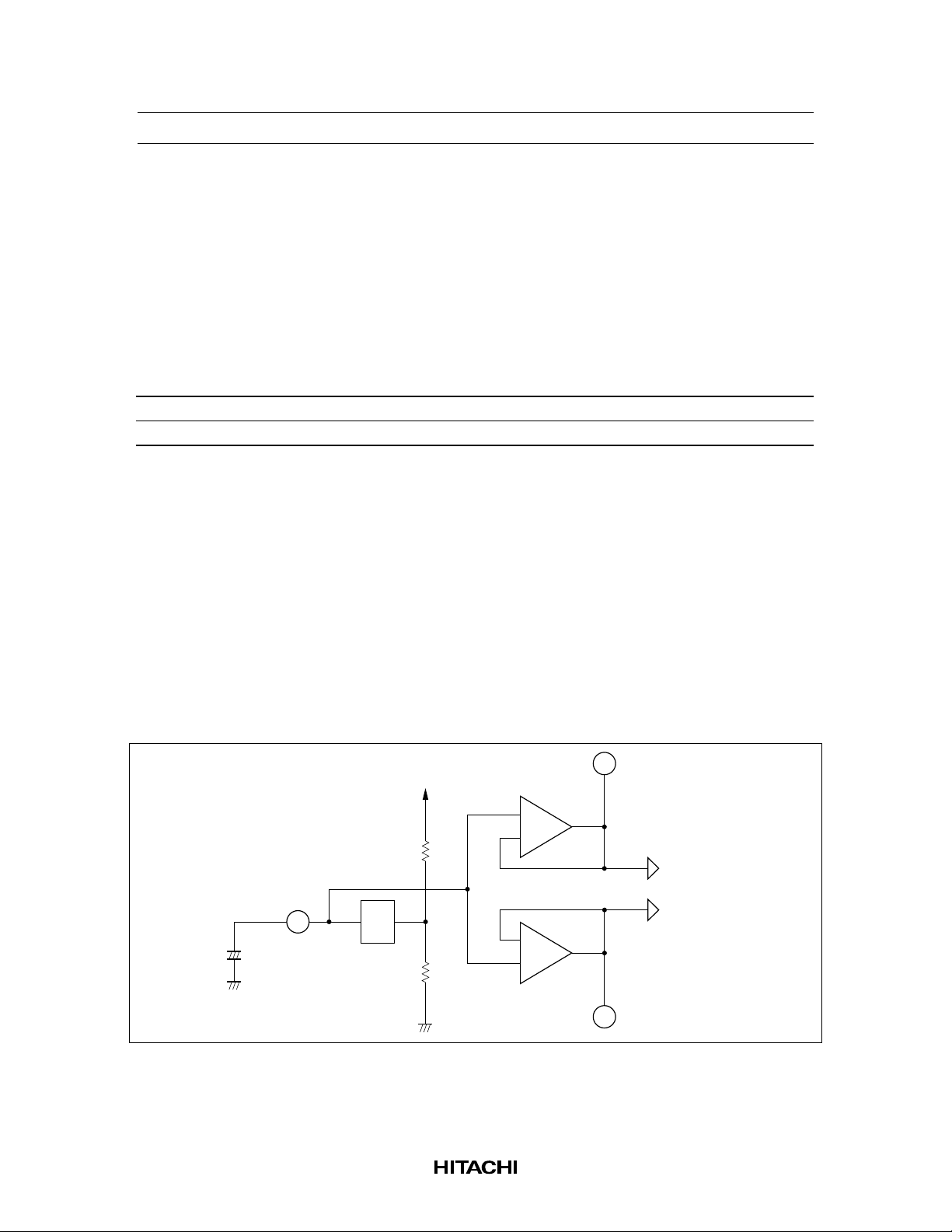
Reference Voltage
For the single supply operation these devices provide the reference voltage of half the supply voltage that is
the signal grounds. As the peculiarity of these devices, the capacitor for the ripple filter is very small about
1/100 compared with their usual value. The Reference voltage are provided for the left channel and the
right channel separately. The block diagram is shown as figure 1.
V
CC
+
–
77
+
1 µF
–
+
61
L channel
reference
R channel
reference
80
Figure 1 The Block Diagram of Reference Voltage Supply
Rev.3, Jun. 1997, page 18 of 73
HA12167FB/HA12169FB
Operating Mode Control
HA12167FB/HA12169FB provides fully electronic switching circuits. All switches are controlled by serial
data.
Table 2 Threshold Voltage (VTH)
Pin No. Lo Hi Unit
42 –0.2 to 1.5 3.5 to 5.3 V
39, 40, 41 –0.2 to 1.0 4.0 to 5.3 V
Notes: 1. Voltages shown above are determined by internal circuits of LSI when take pin 47 (DGND pin) as
reference pin. On split supply use, same VTH can be offered by connecting DGND pin to GND
pin.
This means that it can be controlled directly by micro processor.
2. Each pins are on pulled down with 100 kΩ internal resistor .
Therefore, it will be low-level when each pins are open.
3. Note on serial data inputting
(a) The clock frequency on CLK must be less than 500 kHz.
(b) Over shoot level and under shoot level of input signal must be the value shown below.
When connecting microcomputer or Logic-IC with HA12167FB/HA12169FB directly, there is
apprehension of rash-current under some transition timming of raising voltag e or falling voltage at V
ON/OFF.
CC
For this countermeasure, connect 10 kΩ to 20 kΩ resistor with each pins. It is shown in test circuit on this
data sheet.
In case of changing NR-ON/OFF at the C-mode, for the countermeasure of the noise of pop, perform the
following processes.
In case of changing NR-OFF to NR-ON at C-mode. C-mode, NR-OFF → B-mode, NR-OFF → B-mode,
NR-ON → C-mode, NR-ON.
In case of changing NR-ON to NR-OFF at C-mode. C-mode, NR-ON → B-mode, NR-ON → B-mode,
NR-OFF → C-mode, NR-OFF.
Under 5.3 V
0
Within –0.2 V
Figure 2 Input Level
Rev.3, Jun. 1997, page 19 of 73
HA12167FB/HA12169FB
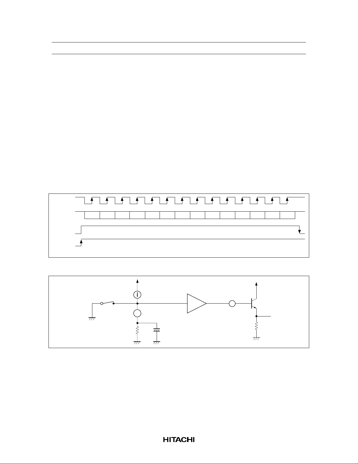
Serial Data Formatting
14 bit shift register is employed.
CLK and data are stored during STB being high and data is latched when STB goes high to low.
Reset goes reset a state when reset low and high releasles reset. (High fixed at use time)
Attention Point of Serial Interface
• Reset goes low condition when a power supply is ON or OFF.
• Characteristics select of Bias DAC is connected with equalizer tape selector.
• Bias DAC register is all low when a time of tape select.
• Bias DAC register is all low and Bias DAC out is dropped low level at compulsion by force.
• Input pin select, REC/PB select and Input volume gain select does not select at the same time.
• Input volume must go mute condition when selected of RPI is input pin select.
CLK
DATA
STB
RESET
012345678910111213
Reset release
Figure 3 Serial Data Timming Chart Figure
MUTE
DAC
Buff
BIAS CONT
+
DACOUT
Figure 4 Bias DAC Output Circuit
Latch of data
Rev.3, Jun. 1997, page 20 of 73
HA12167FB/HA12169FB
Serial Data Formatting
Bit Mode Control Input Voltage Eaqualizer Voltage Basic DAC
No. Reset Reset Reset Reset
0 Tape
selector 1
1 Tape
selector 2
2 Tape
speed
3 Meter
sensitivity
4 Input
selector 1
5 Input
selector 2
6 REC/PB H PB mode selection H R
7 Input
voltage
gain
8 MPX H ON L I-bit 2 L E-bit 2 L B-bit 2 L
9 NR H ON L I-bit 3 L E-bit 3 L B-bit 3 L
10 B/C H C L I-bit 4 L E-bit 4 L B-bit 4 L
11 — — — I-bit 5 H — — B-bit 5 L
12 Registor
selector 1
13 Registor
selector 2
bit 0
bit 1 H L
H Metal Normal
L Crom Normal
H Hi speed selection L I-bit 2 L E-bit 2 L B-bit 2 L
L Normal speed selection
H Meter sensitivity 20 dBupL I-bit 3 L E-bit 3 L B-bit 3 L
L Meter sensitinity normal
bit 4
bit 5 H L
H VRI3 RPI
L VRI2 VRI1
L REC mode selection
H PB mode volume gain H I-bit 1 L E-bit 1 L B-bit 1 L
L Rec mode volume gain
L OFF
L OFF
L B
bit 12
bit 13 H L
H Bias DAC Input volume
L Equalizer volume Mode control
LL
channel
L I-bit 1 L E-bit 1 L B-bit 1 L
L I=bit 4 L E-bit 4 L B-bit 4 L
L I-bit 5 H — — B-bit 5 L
channel
I-bit 0 L L
I-bit 0 L R
channel
channel
E-bit 0 L L
E-bit 0 L R
channel
B-bit o L
B-bit 0
channel
Rev.3, Jun. 1997, page 21 of 73

HA12167FB/HA12169FB
Input Volume Register
I-bit 5 I-bit 4 I-bit 3 I-bit 2 I-bit 1 I-bit 0 Gain
LLLLLLIncrease
LLLLLH↑
LLLLHL:
LLLLHH:
:::::::
::::::↓
HHHHHLDecrease
HHHHHHMute
Equalizer Volume Register
E-bit 4 E-bit 3 E-bit 2 E-bit 1 E-bit 0 Gain
LLLLLIncrease
LLLLH↑
LLLHL:
LLLHH:
::::::
:::::↓
HHHHLDecrease
HHHHHMute
Bias DAC Register
B-bit 5 B-bit 4 B-bit 3 B-bit 2 B-bit 1 B-bit 0 Bias
LLLLLLMute
LLLLLHDecrease
LLLLHL↑
LLLLHH:
:::::::
:::::::
HHHHHL↓
HHHHHHIncrease
Rev.3, Jun. 1997, page 22 of 73

HA12167FB/HA12169FB
MPX ON/OFF Switch
MPX-OFF mode means that signal from input amp doesn’t go through the MPX filter, but signal goes
through the NR circuit after being attenuated 3 dB by internal resistor. Refer to figure 5. For not cause any
level difference between MPX-ON mode and MPX-OFF mode, it is requested to use MPX-filter which has
definitely 3 dB attenuated. And when applying other usage except figure 5,
take consideration to give bias voltage to NR-IN terminal by resistor or so on because internal of NR-IN
terminal has no bias resistor.
Application as for the Dubbing Cassette Deck
HA12167FB/HA12169FB series has unprocessor signal from recording out terminals during playback
mode. So, it is simply applied for dubbing cassette decks.
MPX
filter
2.4 k
IA OUT NR IN TPVref
IA
MPX ON
6 k
14 k
MPX OFF
3 dB ATT
Figure 5 MPX ON/OFF Switch Block Diagram
5.6 k
X 1
10 mH 220 P
1.5 k
BIAS TRAP
NR
processer
Rev.3, Jun. 1997, page 23 of 73

HA12167FB/HA12169FB
A deck
PB EQ
PB EQ
B deck
Compensation
of low
frequency
reagion
VRI 2 VRI 3 REC OUT
PBREC
EQ IN
REC IN VRI 1
HA12167/9
EQ OUT
PB OUT
Figure 6 Application for Dubbing Deck
Injector Current
2
HA12167FB/HA12169FB has logic circuit which is fabricated by I
L into IC. To operate this circuit, it is
required enough injector current. Injector current goes into from the INJ pin (pin 38) and external resistor
is required to connect to this pin for adequate current. The value of external resistor is obtained by using
following equations. And put them with ±10% tolerance value which is calculated. V
connect to V
shown below. Large injector current fear to cause mis-operation of Logic under the
CC
can allow to
INJ
condition of high temperature. Also, small injector current fear to cause mis-operation (stop operation).
Under the condition of low temperature. Therefore, pay attention to have good stability of V
.
INJ
R
=
INJ
V
INJ
=
R
INJ
3.6
+
V
3.6
EE
k
Ω[]
–0.7
Ω
[]
k
Single supply
Split supply
– 0.7
V
INJ
Gain Control of Electronic Volume
HA12167FB/HA12169FB is designed in order to change the gain by DAC fabricated into IC. To reduce
the click noise when changing volume gain instantaneously, required to connect the capacitor and resistor
(CR time constant) to CONT pin (pin 13, 48, 68, 73). These terminals are also be used as output pin of
DAC. Therefore, by forcing voltage and current to these terminals, it is applicable to control volume gain
directly. But, voltage forced to these terminals must be f rom V
/2 –2 V to VCC/2 (for split supply use, –2 V
CC
to 0 V) in this case. And, this case, change of a gain depending on a temperature gets large.
Rev.3, Jun. 1997, page 24 of 73

HA12167FB/HA12169FB
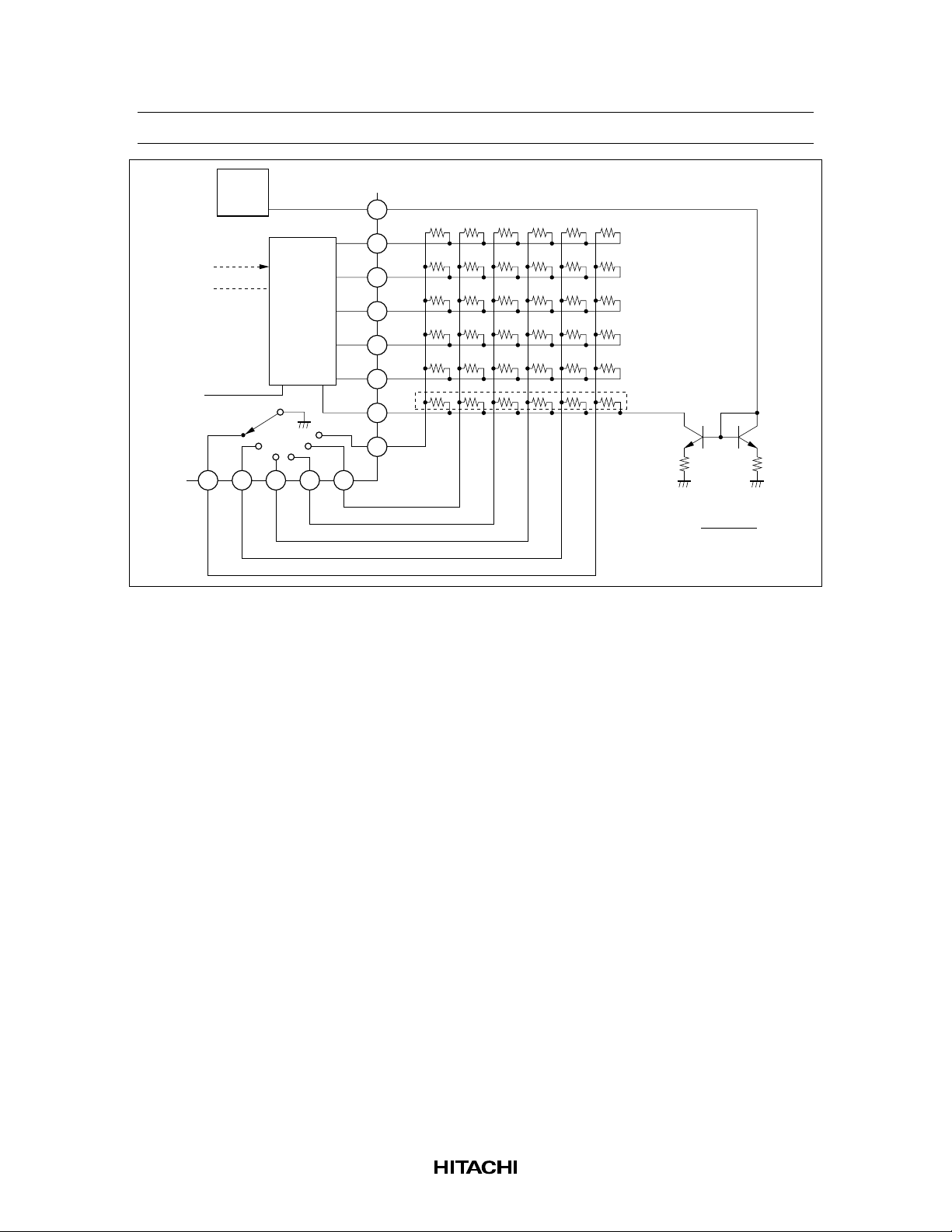
R
INJ
38
3.6 mA
V
INJ
a) Single supply use b) Split supply use
HA12167/9
70
71
34
R
INJ
38
3.6 mA
V
INJ
V
EE
HA12167/9
70
71
34
Figure 7 Injector Current Application
The Tolerances of External Components for Dolby NR-Block
For adequate Dolby NR tracking response, take external components shown below.
For C5, C6, C24, and C25, please employ a few object of the leak, though you can be useful for an
electrolytic-capacitor.
C27
2200 p
±5%
C28
2200 p
±5%
Unit R :
C : F
Ω
BIAS
R31
18 k
±2%
R24
22 k
±2%
59 58 57 56 55 5464
PB OUT
(L)
PB OUT
(R)
234 5 6 7
C2
2200 p
±5%
SS1
(L)
HA12167/9 (REC 1 Chip)
SS1
(R)
R2
22 k
±2%
C3
2200 p
±5%
R26
560
±2%
SS2
(L)
SS2
(R)
R3
560
±2%
C26
2200 p
±5%
CCR
(L)
CCR
(R)
C4
2200 p
±5%
C25
0.1
±10%
HLS
DET(L)
HLS
DET(R)
C5
0.1
±10%
Figure 8 Tolerances of External Components
µ
LLS
DET(L)
LLS
DET(R)
µ
C24
0.1
±10%
C6
0.1
±10%
µ
µ
Rev.3, Jun. 1997, page 25 of 73

HA12167FB/HA12169FB
BIAS DAC
The full-scale of DAC is computed by the formula mentioned below.
2.4
=
V
29
=
V
32
R14: Normal Tape (pin 35)
: Metal Tape (pin 36)
R
15
R
: Chrome Tape (pin 37)
16
The maximum source current of DAC output (pin 29, 32) is 2 mA. Therefor the Bias-osc is drived through
external transisitor of emitter-follower.
Level Meter
The coupling capacitor of LMIN pin (9 pin and 52 pin).
R
R
14 to 16
2.4
14 to 16
×
R V
10
×
R V
13
[]
[]
For these capacitors, please employ a small object of the leak.
Rev.3, Jun. 1997, page 26 of 73
The Application of Equalizer Frequency Response
HA12167FB/HA12169FB
EQ
IN
EQ
VR
R1
Transfer Function:
F/Q
GP
+
Gm 1
–
+
Gm 4
–
R4
C3
+
OP 2
–
R5
+
OP 7
–
–
Gm 2
+
OP 6
+
–
–
Gm 5
+
–
Gm 6
+
GLFM
GH
Figure 9 REC Equalizer Block Diagram
C2
–
OP 5
+
C1
Gm 3
+
OP 3
–
R8
R6
R7
+
–
R10
EQ
OUT
R9
–
OP 4
+
Vout
=
Vin
=
Note: R
R
⋅
Gm5
G
V
9
R
GL
R
REF
....14 pin bias resistance
REF
G
......Gain of EQ-VR
V
1+
⋅
R
8
10
⋅
R
9
1+6.67×10
⋅
1+6.67×10
C3
Gm4
1+
Gm4
–10 FM
C3
Gm6
⋅
Gm5
R
–10
C2
2
⋅
S
2
S
⋅
S
+
Gm1
⋅
S
⋅
R
GH
⋅
S
R
GL
⋅
S
R
FM
+
R
⋅
R
R
GP
⋅
R
4
10
⋅
+
R
6
7
⋅
1+4.5×10
R
R
4
7
⋅
1+
+
R
R
R
5
6
3.0×10
–11
⋅
R
FQ
C3
Gm4
C2
⋅
Gm3
7
–10
⋅
S+ 2.5×10
⋅
S
C1
R
4
⋅
⋅
5
Gm2
⋅
R
FQ
⋅
⋅
R
Gm3
F/Q
S+
R
⋅
⋅
S
R
FQ
–20
Rev.3, Jun. 1997, page 27 of 73

HA12167FB/HA12169FB
Gain
g1
g2
g3
f1 f2 f3 f
Figure 10 REC Equalizer Frequency Response
3dB
BW
g1=
g2
=
g3
=
f1=
f2 =
f3=
BW =
Q=
9
6.67
()
R
REF
9×R
GL
R
REF
9×R
GH
R
REF
+
×
R
R
GP
GH
1
π
×
2
6.67
π
×
2
6.67
1
⋅
2
π
2.25
–10
×
×
10
R
FM
GL
R
–10
×
×
10
×
R
R
FM
GH
0.3
–21
×
×
10
×
R
R
FQ
1
–10
×
×
10
R
F/Q
R
F/Q
×
R
FQ
f3
BW
4
2.78
π
×
3.51
=
when Gain of EQ- VR is center
F/Q
Rev.3, Jun. 1997, page 28 of 73

HA12167FB/HA12169FB
Equalizer Characteristics Control Using a Bias DAC
When only one of the bias DAC channels is used, any one of the six parameters (FM, fQ, f/Q, GH, GL, and
GP) that set the equalizer’s chara cteristics can controlled by the unused bias DAC.
The figure below gives one example.
R
ADJ
37
BIAS ADJ (C)
6 bit
DAC
6 bit
DAC
EQ-
controller
36
35
34
33
32
31
30
29
28
27
26
25
24
23
22
21
FM
fQ
f/Q
GH
GL
GP
HM
BIAS ADJ (M)
BIAS ADJ (N)
GND
BIAS CONT
DAC OUT
V
CC
R’
GP
16 17 18 19 20
NN NC NM HN HC
Figure 11 Bias DAC Control of the GP Parameter
63 R
R = R’ //
GP GP
n: DAC step
ADJ
2 n
Rev.3, Jun. 1997, page 29 of 73

HA12167FB/HA12169FB
Figures 12, 13, and 14 show the characteristics when GP is controlled by a bias DAC.
60
50
40
Gain (dB)
30
20
100 1 k 10 k 30 k
Frequency (Hz)
Figure 12 Equalizer Gain vs. Frequency
B_DAC
0
16
30
46
63
E_DAC = 0 step
VCC = 14 V
RFM = 100 k
RFQ = 51 k
R
F/Q
RGH = 33 k
RGL = 33 k
R’GP = 510 k
R
ADJ
= 51 k
= 20 k
Ω
Ω
Ω
Ω
Ω
Ω
Ω
60
55
50
R’
R’
R’
= 510 k
GP
= 120 k
GP
= 47 k
GP
Ω
Ω
Ω
45
EQ peak gain (dB)
40
35
30
0 10203040506070
B_DAC step
Figure 13 Equalizer Peak Gain vs. DAC Step Characteristics (1)
E_DAC = 0 step
V
= 14 V
CC
R
FM
R
FQ
R
F/Q
R
GH
R
GL
R
ADJ
= 100 k
= 51 k
= 51 k
= 33 k
= 33 k
= 20 k
Ω
Ω
Ω
Ω
Ω
Ω
Rev.3, Jun. 1997, page 30 of 73

HA12167FB/HA12169FB
60
= 33 k (Normal)
R
55
ADJ
R
ADJ
R
ADJ
50
45
EQ peak gain (dB)
40
35
0 10203040506070
B_DAC step
Figure 14 Equalizer Peak Gain vs. DAC Step Characteristics (2)
Ω
= 24 k (Chrome)
Ω
Ω
= 20 k (Metal)
E_DAC = 0 step
= 14 V
V
CC
R
R
R
R
R
R’
FM
FQ
F/Q
GH
GL
= 100 k
= 51 k
= 51 k
= 33 k
= 33 k
= 510 k
GP
Ω
Ω
Ω
Ω
Ω
Ω
When the (variable) width of the DAC step is to be changed, the gain at step 0 or at step 63 must be
changed. The step 0 gain can be changed using R’
as shown in figure 13. Also, R’GP can be switched
GP
using the tape selector, as shown in figure 15. However, it is necessary to take into account that the value
, which sets the step 63 gain, is also used for the output bias. When the load resistance on pin 33 is
of R
ADJ
R
, the following formula gives the output bias, V
L
V
= 2.4 × RL / R
BMAX
ADJ
Therefore, it is possible to compensate the output bias, V
Note: R
should be in the range 16 kΩ to 75 kΩ.
ADJ
BMAX
.
BMAX
for the R
setting by changing RL.
ADJ
Rev.3, Jun. 1997, page 31 of 73
HA12167FB/HA12169FB
6 bit
DAC
EQ-
controler
16 17 18 19 20
NN NC NM HN HC
28
27
26
25
24
23
22
21
FM
fQ
f/Q
GH
GL
GP
HM
R’
GP
R = R’ //
GP GP
n: DAC step
63 R
ADJ
2 n
Figure 15 Switch by Tape Select
Rev.3, Jun. 1997, page 32 of 73

HA12167FB/HA12169FB
Quiescent Current vs. Supply Voltage (1)
38
37
36
35
34
33
Quiescent Current (mA)
32
REC NR-OFF
REC NR-B
31
REC NR-C
30
81012141618
Supply Voltage (V) RPIin I.DAC=0
No.Signal
Quiescent Current vs. Supply Voltage (2)
38
37
36
35
34
33
Quiescent Current (mA)
32
PB NR-OFF
PB NR-B
31
PB NR-C
30
81012141618
Supply Voltage (V) RPIin I.DAC=0
No.Signal
12
Encode Boost vs. Frequency (1) HA12167FB
: 0 dB
: –10 dB
10
: –20 dB
: –30 dB
: –40 dB
NR-B
8
V =14 V
CC
V =15 V
CC
6
V =12 V
CC
Encode Boost (dB)
4
2
0
100 1 k 10 k 100 k
Frequency (Hz)
Rev.3, Jun. 1997, page 33 of 73

HA12167FB/HA12169FB
25
Encode Boost vs. Frequency (2) HA12167FB
: 0 dB
: –20 dB
20
: –30 dB
: –40 dB
: –60 dB
NR-C
15
10
V =15 V
CC
V =12 V, 14 V
CC
5
Encode Boost (dB)
0
–5
–10
100 1 k 10 k 100 k
Frequency (Hz)
Encode Boost vs. Frequency (3) HA12169FB
12
: 0 dB
: –10 dB
10
: –20 dB
: –30 dB
: –40 dB
NR-B
8
V =14 V
CC
V =15 V
CC
6
V =11 V
CC
Encode Boost (dB)
4
2
0
100 1 k 10 k 100 k
Rev.3, Jun. 1997, page 34 of 73
Frequency (Hz)

HA12167FB/HA12169FB
25
20
15
10
5
Encode Boost (dB)
0
–5
–10
100 1 k 10 k 100 k
40
Encode Boost vs. Frequency (4) HA12169FB
: 0 dB
: –20 dB
: –30 dB
: –40 dB
V =15 V
CC
: –60 dB
NR-C
V =11 V, 14 V
CC
Frequency (Hz)
Input Amp. Gain vs. Frequency (1) HA12167FB
PBOUT
20
RECOUT
0
–20
Input Amp. Gain (dB)
–40
RECmode
NR-OFF
V
=14 V
CC
–60
10 100 1 k 10 k 100 k 1 M
Frequency (Hz)
Rev.3, Jun. 1997, page 35 of 73

HA12167FB/HA12169FB
Input Amp. Gain vs. Frequency (2) HA12167FB
40
20
0
–20
PBOUT
RECOUT
Input Amp. Gain (dB)
–40
–60
10 100 1 k 10 k 100 k 1 M
Frequency (Hz)
Input Amp. Gain vs. Frequency (3) HA12169FB
40
PBOUT
20
RECOUT
0
–20
Input Amp. Gain (dB)
–40
–60
10 100 1 k 10 k 100 k 1 M
Frequency (Hz)
PBmode
NR-OFF
V =14 V
CC
RECmode
NR-OFF
V
=14 V
CC
RPI
Rev.3, Jun. 1997, page 36 of 73

40
20
–20
HA12167FB/HA12169FB
Input Amp. Gain vs. Frequency (4) HA12169FB
PBMODE PBOUT
RECMODE RECOUT
0
Input Amp. Gain (dB)
–40
–60
10 100 1 k 10 k 100 k 1 M
Frequency (Hz)
PBmode
NR-OFF
V =14 V
CC
Rev.3, Jun. 1997, page 37 of 73

HA12167FB/HA12169FB
Total Harmonic Distortion vs. Output Level (1)
10
1.0
0.1
Total Harmonic Distortion T.H.D. (%)
0.01
–15 –10 –50 51015
: 10 kHz
: 1 kHz
: 100 Hz
V = 14 V, RPIin, RECmode
CC
RECOUT, 0 dB = 300 mVrms,
25 Hz HPF, 80 kHz LPF,
NR-OFF
Output Level Vout (dB)
Total Harmonic Distortion vs. Output Level (2)
10
: 10 kHz
: 1 kHz
: 100 Hz
V = 14 V, RPIin, RECmode
CC
1.0
0.1
Total Harmonic Distortion T.H.D. (%)
0.01
–15 –10 –50 51015
RECOUT, 0 dB = 300 mVrms,
25 Hz HPF, 80 kHz LPF,
NR-B
Output Level Vout (dB)
Rev.3, Jun. 1997, page 38 of 73

HA12167FB/HA12169FB
Total Harmonic Distortion vs. Output Level (3)
10
: 10 kHz
: 1 kHz
: 100 Hz
V = 14 V, RPIin, RECmode
CC
RECOUT, 0 dB = 300 mVrms,
25 Hz HPF, 80 kHz LPF,
1.0
NR-C
0.1
Total Harmonic Distortion T.H.D. (%)
0.01
–15 –10 –50 51015
Output Level Vout (dB)
Total Harmonic Distortion vs. Output Level (4)
10
: 10 kHz
: 1 kHz
: 100 Hz
1.0
0.1
Total Harmonic Distortion T.H.D. (%)
0.01
–15 –10 –50 51015
V = 14 V, RPIin, PBmode
CC
PBOUT, 0 dB = 775 mVrms,
25 Hz HPF, 80 kHz LPF,
NR-OFF
Output Level Vout (dB)
Rev.3, Jun. 1997, page 39 of 73

HA12167FB/HA12169FB
Total Harmonic Distortion vs. Output Level (5)
10
: 10 kHz
: 1 kHz
: 100 Hz
1.0
0.1
Total Harmonic Distortion T.H.D. (%)
0.01
–15 –10 –50 51015
10
1.0
V = 14 V, RPIin, PBmode
CC
PBOUT, 0 dB = 775 mVrms,
25 Hz HPF, 80 kHz LPF,
NR-B
Output Level Vout (dB)
Total Harmonic Distortion vs. Output Level (6)
: 10 kHz
: 1 kHz
: 100 Hz
V = 14 V, RPIin, PBmode
CC
PBOUT, 0 dB = 775 mVrms,
25 Hz HPF, 80 kHz LPF,
NR-C
0.1
Total Harmonic Distortion T.H.D. (%)
0.01
Rev.3, Jun. 1997, page 40 of 73
–15 –10 –50 51015
Output Level Vout (dB)

HA12167FB/HA12169FB
Maximum Output Level vs.
Supply Voltage (1) HA12167FB
20
: NR-OFF
: NR-B
: NR-C
15
10
RECmode, RECOUT
RPIin, f = 1 kHz
Maximum Output Level Vo max (dB)
0 dB = 300 mVrms
T.H.D. = 1%
5
810121416
Supply Voltage V (V)
CC
Maximum Output Level vs.
Supply Voltage (2) HA12167FB
20
: NR-OFF
: NR-B
: NR-C
15
10
PBmode, PBOUT
RPIin, f = 1 kHz
Maximum Output Level Vo max (dB)
0 dB = 775 mVrms
T.H.D. = 1%
5
810121416
Supply Voltage V (V)
CC
Maximum Output Level vs.
Supply Voltage (3) HA12169FB
20
: NR-OFF
: NR-B
: NR-C
15
10
RECmode,RPIin,RECOUT
0 dB = 300 mVrms
25 Hz HPF +19 kHz LPF
Maximum Output Level Vo max (dB)
T.H.D. = 1%
5
810121416
Supply Voltage V (V)
CC
Maximum Output Level vs.
Supply Voltage (4) HA12169FB
20
: NR-OFF
: NR-B
: NR-C
15
10
PBmode,RPIin,PBOUT
0 dB = 580 mVrms
25 Hz HPF +19 kHz LPF
Maximum Output Level Vo max (dB)
T.H.D. = 1%
5
810121416
Supply Voltage V (V)
CC
Rev.3, Jun. 1997, page 41 of 73

HA12167FB/HA12169FB
Signal to Noise Ratio vs.
Supply Voltage (1) HA12167FB
95
PB NR-C
90
PB NR-B
REC NR-OFF
PB NR-OFF
80
REC NR-B
70
Signal to Noise Ratio S/N (dB)
REC NR-C
RPIin, Rg = 5.1 k CCIR/ARMΩ
60
810121416
Supply Voltage V (V)
CC
Signal to Noise Ratio vs.
Supply Voltage (2) HA12169FB
95
90
PB NR-C
PB NR-B
REC NR-OFF
80
PB NR-OFF
REC NR-B
70
Signal to Noise Ratio S/N (dB)
REC NR-C
RPIin, Rg = 5.1 k CCIR/ARMΩ
60
810121416
Supply Voltage V
CC
(V)
Crosstalk vs. Frequency (1)
(L→R)
–20
RECVol, VRI1in, RECOUTout
I. DAC = 0 EQ. DAC = 31
–40
–60
V
= 14
CC
NR-C
NR-B
–80
NR-OFF
Crosstalk (dB)
–100
–120
100 1 k 10 k 100 k
Frequency (Hz)
Rev.3, Jun. 1997, page 42 of 73

HA12167FB/HA12169FB
Crosstalk vs. Frequency (2)
–20
PBVol, VRI1in, PBOUTout
–40
–60
–80
Crosstalk (dB)
–100
–120
I. DAC = 0 EQ. DAC = 31
V = 14
CC
100 1 k 10 k 100 k
Crosstalk vs. Frequency (3)
(VRI1 VRI2, VRI3, RPI)
–20
(L→R)
NR-OFF
NR-B
NR-C
Frequency (Hz)
–40
–60
–80
Crosstalk (dB)
–100
–120
RECVol, VRI1in, PBOUTout
I. DAC = 0, V = 14 V
100 1 k 10 k 100 k
CC
VRI 2
VRI 3
RPI
Frequency (Hz)
Rev.3, Jun. 1997, page 43 of 73

HA12167FB/HA12169FB
–20
Crosstalk vs. Frequency (4)
(VRI1 VRI2, VRI3, RPI)
–40
–60
–80
Crosstalk (dB)
–100
–120
–20
PBVol, VRI1in, PBOUTout
I. DAC = 0, V = 14 V
100 1 k 10 k 100 k
CC
VRI 2
VRI 3
RPI
Frequency (Hz)
Crosstalk vs. Frequency (5)
(VRI2 VRI1, VRI3, RPI)
–40
–60
–80
Crosstalk (dB)
–100
–120
Rev.3, Jun. 1997, page 44 of 73
RECVol, VRI2in, PBOUTout
I. DAC = 0, Vcc = 14 V
100 1 k 10 k 100 k
VRI 3
RPI
VRI 1
Frequency (Hz)

–20
HA12167FB/HA12169FB
Crosstalk vs. Frequency (6)
(VRI2 VRI1, VRI3, RPI)
–40
–60
–80
Crosstalk (dB)
–100
–120
–20
PBVol, VRI2in, PBOUTout
I. DAC = 0, V = 14 V
100 1 k 10 k 100 k
CC
VRI 3
VRI 1
RPI
Frequency (Hz)
Crosstalk vs. Frequency (7)
(VRI3 VRI1, VRI2, RPI)
–40
–60
–80
Crosstalk (dB)
–100
–120
RECVol, VRI3in, PBOUTout
I. DAC = 0, V = 14 V
100 1 k 10 k 100 k
CC
VRI 2
RPI
VRI 1
Frequency (Hz)
Rev.3, Jun. 1997, page 45 of 73

HA12167FB/HA12169FB
–20
Crosstalk vs. Frequency (8)
(VRI3 VRI1, VRI2, RPI)
–40
–60
–80
Crosstalk (dB)
–100
–120
–20
–40
PBCVol, VRI3in, PBOUTout
I. DAC = 0, V = 14 V
100 1 k 10 k 100 k
REC Vol, RPIin, PBOUTout
I.DAC = 0, V = 14 V
CC
VRI 2
RPI
VRI 1
Frequency (Hz)
Crosstalk vs. Frequency (9)
(RPI VRI 1, VRI 2, VRI 3)
CC
VRI 3
–60
–80
Crosstalk (dB)
–100
–120
100 1 k 10 k 100 k
Rev.3, Jun. 1997, page 46 of 73
VRI 2
VRI 1
Frequency (Hz)

HA12167FB/HA12169FB
Crosstalk vs. Frequency (10)
(RPI VRI 1, VRI 2, VRI 3)
–20
PB Vol, RPIin, PBOUTout
I.DAC = 0, V = 14 V
–40
–60
–80
Crosstalk (dB)
–100
–120
100 1 k 10 k 100 k
CC
VRI 3
VRI 2
VRI 1
Frequency (Hz)
Ripple Rejection Ratio vs. Frequency (1)
20
0
–20
–40
–60
Ripple Rejection Ratio R.R.R. (dB)
–80
10 100 1 k 10 k 100 k 1 M
RECVol, VRI3in, RECOUTout
I.DAC = 0, V = 14 V
CC
Frequency (Hz)
C
B
OFF
Rev.3, Jun. 1997, page 47 of 73

HA12167FB/HA12169FB
20
Ripple Rejection Ratio vs. Frequency (2)
0
–20
–40
–60
Ripple Rejection Ratio R.R.R. (dB)
–80
10 100 1 k 10 k 100 k 1 M
0
–10
RECVol, VRI3in, EQOUTout
I.DAC = 0, EQ, DAC = 0
V = 14 V
CC
Frequency (Hz)
Ripple Rejection Ratio vs. Frequency (3)
PBVol, VRI3in, PBOUTout
I.DAC = 0, V = 14 V
CC
C
B
OFF
–20
–30
Ripple Rejection Ratio R.R.R. (dB)
–40
–45
10 100 1 k 10 k 100 k 1 M
Rev.3, Jun. 1997, page 48 of 73
OFF
B
C
Frequency (Hz)

HA12167FB/HA12169FB
Input Volume Gain vs. DAC Step (1) HA12167FB
40
20
0
–20
Input Volume Gain (dB)
–40
–60
Input Volume Gain vs. DAC Step (2) HA12167FB
35
30
25
Input Volume Gain (dB)
20
VCC = 14 V, RECVol
f = 1 kHz
VRI1in, PBOUTout
80 kHz LPF, 400 Hz HPF
0 102030405060
DAC Step
VCC = 14 V, PBVol
f = 1 kHz
VRI2in, PBOUTout
80 kHz LPF, 400 Hz HPF
15
0 102030405060
DAC Step
Rev.3, Jun. 1997, page 49 of 73

HA12167FB/HA12169FB
Input Volume Gain vs. DAC Step (3) HA12169FB
40
20
0
–20
Input Volume Gain (dB)
–40
–60
Input Volume Gain vs. DAC Step (4) HA12167FB
35
30
25
Input Volume Gain (dB)
20
VCC = 14 V, RECVol
f = 1 kHz
VRI1in, PBOUTout
80 kHz LPF, 400 Hz HPF
0 102030405060
DAC Step
VCC = 14 V, PBVol
f = 1 kHz
VRI2in, PBOUTout
80 kHz LPF, 400 Hz HPF
Rev.3, Jun. 1997, page 50 of 73
15
0 102030405060
DAC Step

Signal to Noise Ratio vs. DAC Step (1)
75
HA12167FB/HA12169FB
80
85
90
Signal to Noise Ratio S/N (dB)
VCC = 14 V, RECVol
VRI1in, PBOUTout
95
0 102030405060
Signal to Noise Ratio vs. DAC Step (2)
60
DIN-AUDIO
CCIR-ARM
JIS-A
DAC Step
65
70
DIN-AUDIO
75
Signal to Noise Ratio S/N (dB)
80
0 102030405060
JIS-A
VCC = 14 V, PBVol
VRI2in, PBOUTout
DAC Step
CCIR-ARM
Rev.3, Jun. 1997, page 51 of 73

HA12167FB/HA12169FB
20
15
10
5
Maximum Output Voltage Vo max (dB) (0dB = 775 mVrms)
0 102030405060
Maximum Output Voltage vs.
DAC Step (1) HA12167FB
VCC = 14 V
RECVol, f = 1 kHz
VRI1in, PBOUTout
T.H.D. = 1 %
80 kHz LPF, 400 Hz HPF
DAC Step
Maximum Output Voltage vs.
20
15
10
5
Maximum Output Voltage Vo max (dB) ( dB = 775 mVrms)
0 102030405060
DAC Step (2) HA12167FB
V =14 V
CC
PBVol, f=1 kHz
VRI2in, PBOUTout T.H.D.=1%
80 kHz LPF, 400 Hz HPF
DAC Step
Rev.3, Jun. 1997, page 52 of 73

HA12167FB/HA12169FB
Maximum Output Voltage vs.
22.5
17.5
12.5
7.5
2.5
Maximum Output Voltage Vo max (dB) (0 dB = 580 mVrms)
0 102030405060
DAC Step (3) HA12169FB
VCC = 14 V
RECVol, f = 1 kHz
VRI1in, PBOUTout
T.H.D. = 1 %
80 kHz LPF, 25 Hz HPF
DAC Step
Maximum Output Voltage vs.
22.5
17.5
12.5
7.5
2.5
Maximum Output Voltage Vo max (dB) (0 dB = 580 mVrms)
0 102030405060
DAC Step (4) HA12169FB
V =14 V
CC
PBVol, f=1 kHz
VRI2in, PBOUTout T.H.D.=1%
80 kHz LPF, 25 Hz HPF
DAC Step
Rev.3, Jun. 1997, page 53 of 73
HA12167FB/HA12169FB
10
Total Harmonic Distortion vs. DAC Step (1)
f=100 Hz RECmode
VRI1in PBOUTout
V =14 V
CC
80 kHz LPF
1.0
0.1
Total Harmonic Distortion T.H.D. (%)
0.01
0102030405060
DAC Step
Total Harmonic Distortion vs. DAC Step (2)
10
f=1 kHz RECmode
VRI1in PBOUTout
V =14 V
CC
80 kHz LPF
+10 dB
–10 dB
0 dB
Total Harmonic Distortion T.H.D. (%)
0.01
Rev.3, Jun. 1997, page 54 of 73
1.0
0.1
0102030405060
DAC Step
+10 dB
0 dB
–10 dB

Total Harmonic Distortion vs. DAC Step (3)
10
f=10 kHz RECmode
VRI1in PBOUTout
V =14 V
CC
80 kHz LPF
HA12167FB/HA12169FB
1.0
0.1
Total Harmonic Distortion T.H.D. (%)
0.01
0 102030405060
DAC Step
Total Harmonic Distortion vs. DAC Step (4)
10
f=100 kHz PBmode
VRI2in PBOUTout
V =14 V 80 kHz LPF
CC
+10 dB
0 dB
–10 dB
1.0
–10 dB
0.1
0 dB
Total Harmonic Distortion T.H.D. (%)
+10 dB
0.01
0 102030405060
DAC Step
Rev.3, Jun. 1997, page 55 of 73

HA12167FB/HA12169FB
10
1.0
0.1
Total Harmonic Distortion T.H.D. (%)
0.01
0102030405060
Total Harmonic Distortion vs. DAC Step (5)
f=1 kHz PBmode
VRI2in PBOUTout
V =14 V 80 kHz LPF
CC
–10 dB
0 dB
+10 dB
DAC Step
Total Harmonic Distortion vs. DAC Step (6)
10
f=10 kHz PBmode
VRI2in PBOUTout
V =14 V 80 kHz LPF
CC
1.0
–10 dB
0.1
0 dB
Total Harmonic Distortion T.H.D. (%)
+10 dB
0.01
0 102030405060
DAC Step
Rev.3, Jun. 1997, page 56 of 73
HA12167FB/HA12169FB
REC Volume Maximam Input
Level vs. Supply Voltage
15
10
5
RECVol I.DAC Step=42
VRI1in PBOUTout f=1 kHz
REC Volume Maximam Input Level Vin Max (dBs)
0
810121416
Supply Voltage (V)
Volume Gain vs. Frequency (1) HA12167FB
I.DAC 0
20
0
–20
–40
Volume Gain (dB)
–60
–70
VRI1 PBOUT RECVolume V =14 V
10 100 1 k 10 k 100 k 1 M
CC
Frequency (Hz)
I.DAC 10
I.DAC 20
I.DAC 30
I.DAC 40
I.DAC 50
I.DAC 62
Rev.3, Jun. 1997, page 57 of 73

HA12167FB/HA12169FB
Volume Gain vs. Frequency (2) HA12167FB
50
40
I.DAC 0
30
20
Volume Gain (dB)
10
VRI 2 PBOUT PBVolume V =14 V
0
10 100 1 k 10 k 100 k 1 M
Volume Gain vs. Frequency (3) HA12169FB
STEP 0
20
0
–20
STEP 10
I.DAC 32
I.DAC 62
CC
Frequency (Hz)
STEP 20
STEP 30
STEP 40
STEP 50
–40
Volume Gain (dB)
–60
–70
VRI1 PBOUT RECVolume V =14 V
10 100 1 k 10 k 100 k 1 M
Rev.3, Jun. 1997, page 58 of 73
STEP 60
STEP 62
CC
Frequency (Hz)

40
HA12167FB/HA12169FB
Volume Gain vs. Frequency (4) HA12169FB
32
24
16
STEP 0
STEP 32
STEP 62
Volume Gain (dB)
8
VRI 2 PBOUT PBVolume V =14 V
0
10 100 1 k 10 k 100 k 1 M
CC
Frequency (Hz)
Input Volume Gain vs.
Input Volume Gain vs.
Temperature (1) HA12167FB
Temperature (2) HA12167FB
35
20
30
0
RECVol
VRI1in PBOUTout
V =14 V
CC
20
f=1 kHz
400 Hz HPF
80 kHz LPF
Input Volume Gain (dB)
40
60
40 20 0 20 40 60 80
Temperature Ta (
: 0 step
: 10 step
: 20 step
: 30 step
: 62 step
C)
25
Input Volume Gain (dB)
PBVol
20
VRI2in PBOUTout
f=1 kHz
V =14 V
CC
400 Hz HPF
80 kHz LPF
15
40 20 0 20 40 60 80
Temperature Ta (
Rev.3, Jun. 1997, page 59 of 73
: 0 step
: 32 step
: 62 step
C)

HA12167FB/HA12169FB
Maximum Output Level vs. Temperature (1)
20
15
10
RECVol
VRI1in PBOUTout
V =14 V T.H.D.=1%
CC
5
400 Hz HPF
Maximum Output Level Vomax (dBs)
80 kHz LPF
: 0 step
: 16 step
: 25 step
: 30 step
0
40 20 0 20 40 60 80
Temperature Ta (
C)
Maximum Output Level vs. Temperature (2)
20
15
10
PBVol
VRI2in PBOUTout
V =14 V T.H.D.=1%
CC
5
400 Hz HPF
Maximum Output Level Vomax (dBs)
80 kHz LPF
: 0 step
: 32 step
: 62 step
0
40 20 0 20 40 60 80
Temperature Ta (
C)
Level Meter Output vs. Input Level
V = 14 V
4.0
CC
fin = 1 kHz
0 dB = 775
mVrms
3.0
2.0
Level Meter Output (V)
1.0
0
–80 –60 –40 –20 0 20 40
Input Level Vin (dB)
Level Meter Output vs.
Supply Voltage (1) HA12167FB
4
3
2
: 0 dB range Vin=+12 dB
: 0 dB range Vin=0 dB
: 0 dB range Vin=–20 dB
Level Meter Output (V)
: 20 dB range Vin=–20 dB
1
0
8 1012141618
Supply Voltage (V)
Rev.3, Jun. 1997, page 60 of 73

HA12167FB/HA12169FB
Level Meter Output vs.
Supply Voltage (2) HA12169FB
4
3
2
: 0 dB range Vin=+12 dB
: 0 dB range Vin=0 dB
: 0 dB range Vin=–20 dB
Level Meter Output (V)
: 20 dB range Vin=–20 dB
1
0
8 1012141618
Supply Voltage (V)
Level Meter Output vs. Temperature
4.0
3.0
2.0
: 0 dB range 0 dB
: 0 dB range 12 dB
: 20 dB range 5 dB
Level Meter Output LMout (V)
1.0
: 20 dB range 20 dB
f = 1 kHz V = 14 V
0
40 20 0 20 40 60 80
Temperature Ta (
CC
C)
Level Meter Output vs. Frequency
3.2
: Normal range Vin=0 dB
3.0
2.8
2.6
2.4
Level Meter Output (V)
2.2
2.0
20 100 1 k 10 k 50 k
Frequency (Hz)
: 20 dBup range Vin=–20 dB
V = 14 V
CC
Rev.3, Jun. 1997, page 61 of 73

HA12167FB/HA12169FB
55
Equalizer Gain vs. Frequency (1)
50
40
30
20
Equalizer Gain (dB)
10
(1) (2) (3) (4) (5) (6)
NN HN NC HC NM HM
RGP
33 k 33 k 33 k 33 k 47 k 47 k
RGL
33 k 33 k 51 k 51 k 51 k 51 k
33 k 33 k 51 k 51 k 51 k 51 k
RGH
51 k 20 k 51 k 20 k 51 k 20 k
RF/Q
51 k 27 k 51 k 27 k 51 k 27 k
RFQ
100 k 100 k 100 k 100 k 100 k 100 k
RFM
EQin EQout V =14 V EQ.DAC=0 Vin=–38 dBS
CC
(5)
(3)
(1)
(4)
(2)
(6)
5
10 100 1 k 10 k 100 k 1 M
Frequency (Hz)
Equalizer Gain vs. Frequancy (2)
50
40
30
20
Equalizer Gain (dB)
DAC 16
DAC 0
DAC 30
10
EQin EQout V =14 V Vin=–36 dBS
0
10 100 1 k 10 k 100 k 1 M
CC
Frequency (Hz)
Equalizer Gain vs. Frequancy (3)
40
0
DAC 30
–40
–80
Equalizer Gain
DAC 31
–120
EQin EQout V =14 V Vin=–36 dBS
–160
10 100 1 k 10 k 100 k 1 M
CC
Frequency (Hz)
Rev.3, Jun. 1997, page 62 of 73
Total Harmonic Distortion vs.
50
Equalizer Output Level (1)
EQin EQout 0 step
V
= 14 V, 0 dB = –1 dBs
CC
HA12167FB/HA12169FB
3.5 kHz
10
1.0
350 Hz
Total Harmonic DIstortion T.H.D. (%)
0.1
–30 –20 –10 0 10 20 30
Equalizer Output Level (dB)
Total Harmonic Distortion vs.
50
10
Equalizer Output Level (2)
EQin EQout 16 step
V
= 14 V, 0 dB = –4 dBs
CC
10 kHz
15 kHz
315 Hz
1 kHz
15 kHz
6.3 kHz
3.15 kHz
6.3 kHz
1.0
Total Harmonic DIstortion T.H.D. (%)
0.1
–30 –20 –10 0 10 20 30
Equalizer Output Level (dB)
10 kHz
1 kHz
Rev.3, Jun. 1997, page 63 of 73

HA12167FB/HA12169FB
50
10
Total Harmonic Distortion vs.
Equalizer Output Level (3)
EQin EQout 30 step
V
= 14 V, 0 dB = –8 dBs
CC
315 Hz
1.0
15 kHz
10 kHz
Total Harminic Distortion T.H.D. (%)
0.1
–30 –20 –10 0 10 20 30
Equalizer Output Level (dB)
Equalizer Amp. Gain vs. R
45
EQin EQout V = 14 V
Vin = –46 dBS = 0 dB
EQ.DAC = 0 Step
40
R = R = 33 k
GH GP
R = R = 51 k
FQ F/Q
R = 100 k
FM
CC
35
30
1 kHz
6.3 kHz
3.15 kHz
GL
25
Equalizer Amp. Gain GL (dB)
20
15
Rev.3, Jun. 1997, page 64 of 73
: 316 Hz
: 1 kHz
5 k 10 k 30 k 100 k 300 k 1 M
GL
)
R (

HA12167FB/HA12169FB
45
Equalizer Amp. Gain vs. R
EQin EQout V = 14 V
CC
GH
Vin = –46 dBS = 0 dB
EQ.DAC = 0 Step
40
R = 33 k
GL
R = 16 k
GP
35
R = R = 24 k
R = 390 k
FQ
FM
F/Q
f = 6.3 kHz
30
25
Equalizer Amp. Gain GH (dB)
20
15
5 k 10 k 30 k 100 k 300 k 1 M
GH
)
GP
R (
Equalizer Amp. Gain vs. R
65
60
EQin EQout
Vcc = 14 V
EQ.DAC = 0 Step
55
50
R = R = 33 k
R = R = 51 k
R = 100 k
f = 19 kHz
GL
FQ
FM
GH
F/Q
45
Equalizer Amp. Gain GP (dB)
40
35
5 k 10 k 30 k 100 k 300 k 1 M
R ( )
GP
Rev.3, Jun. 1997, page 65 of 73

HA12167FB/HA12169FB
100 k
Equalizer Cutoff Frequency vs. R
EQin EQout
Vcc = 14 V
EQ.DAC=0 Step
10 k
1 k
Equalizer Cutoff Frequency (Hz)
R = 120 k
GL
R = 7.5 k
GH
R = R = 24k
FQ F/Q
R = 16 k
GP
100
5 k 10 k 30 k 100 k 300 k 500 k
RFM ( )
FM
1 M
Equalizer Peak Frequency vs. R
EQin EQout
Vcc = 14 V
EQ.DAC = 0 Step
100 k
10 k
R
Equalizer Peak Frequency fo (Hz)
F/Q
: 12 k
: 24 k
: 51 k
: 100 k
: 200 k
: 390 k
1 k
5 k 10 k 30 k 100 k 300 k 500 k
RFQ ( )
FQ
Rev.3, Jun. 1997, page 66 of 73

HA12167FB/HA12169FB
Equalizer Quality Factor vs. R
FQ
15
EQin EQout
Vcc = 14 V
EQ.DAC = 0 Step
Vin = - 50 dBs
R =
10
F/Q
: 390 k
: 200 k
: 100 k
: 51 k
: 24 k
: 12 k
5
Equalizer Quality Factor Q.
0
5 k 10 k 30 k 100 k 300 k 1 M
( )
R
FQ
Equalizer Gain vs. DAC Step
31
V
= 14 V
CC
EQin EQOUTout
f = 1 kHz
Vin = –26dBs
26
EQ. Gain (dB)
21
16
0102030
DAC Step
Rev.3, Jun. 1997, page 67 of 73

HA12167FB/HA12169FB
–60
–65
EQ. Noise (dBs)
–70
–75
0102030
15
Equalizer Vo max, Vin max vs. DAC Step
Equalizer Noise vs. DAC Step
V
CC
JIS-A filter
DAC Step
Vo max
= 14 V
0
10
5
Equalizer Vo max (dBs)
0
Rev.3, Jun. 1997, page 68 of 73
Vin max
EQin EQout
f = 1 kHz V
T.H.D. = 1%
10 20 30
DAC Step
= 14 V
cc
–5
–10
Equalizer Vin max (dBs)
–15

HA12167FB/HA12169FB
Equalizer Vo max, Vin max vs. Supply Voltage
15
EQin EQout
0
f = 1 kHz
T.H.D.=1%
10
5
Equalizer Vo max (dBs)
0
–3
Vo max
: 0 Step
: 16 Step
: 30 Step
Vin max
: 0 Step
: 16 Step
: 30 Step
–5
–10
–15
–18
8 10121416
Supply Voltage (V)
Equalizer Vo max, Vin max vs. Temperature
15 0
Vo max
Equalizer Gain vs. Temperature
30
25
20
Gain (dB)
Equalizer Vin max (dBs)
15
10
40 20 0 20 40 60 80
0 step
16 step
30 step
V = 14 V, Vin = 26 dBs
CC
f = 1 kHz
Temperature Ta (°C)
10
5
Vin max
Equalizer Vo max (dBs)
EQin EQout V = 14 V
0
CC
0 step f = 1 kHz
3
40 20 0 20 40 60 80
Temperature Ta (°C)
5
10
Equalizer Vin max (dBs)
15
18
90
Rev.3, Jun. 1997, page 69 of 73

HA12167FB/HA12169FB
Maximum Output Level vs. BIAS Adjust Register
14
12
10
8
6
4
Maximum Output Level (V)
2
0
5 k 10 k 100 k 1 M
V = 14 V
CC
B. DAC = 63 Step
Normal
Crom
Metal
BIAS Adjust Register R
ADJ
(Ω)
14
12
10
8
6
4
DAC Output Level (V)
2
DAC Output Level vs. DAC Step
V =14 V
CC
Metal : 20 k
Crom : 24 k
Normal : 33 k
0 102030405060
Ω
Ω
Ω
Metal
DAC Step
Crom
Normal
Rev.3, Jun. 1997, page 70 of 73

Bias Vomax vs. Supply Voltage
20
Metal
18
16
14
12
Bias Vo max (V)
10
Crom
Normal
HA12167FB/HA12169FB
VCC Line
8
6
4
810121416
Supply Voltage (V)
B.DAC=63 step
R =10 k
ADJ
Ω
Rev.3, Jun. 1997, page 71 of 73

HA12167FB/HA12169FB
Package Dimensions
17.2 ± 0.3
14
60
41
Unit: mm
61
17.2 ± 0.3
80
1
0.32 ± 0.08
0.30 ± 0.06
0.12
0.83
0.10
20
40
0.65
21
M
2.70
3.05 Max
0.17 ± 0.05
0.15 ± 0.04
1.6
0˚ – 8˚
+0.15
–0.10
0.10
Hitachi Code
JEDEC Code
EIAJ Code
Weight
0.8 ± 0.3
FP-80A
—
ED-7404A
1.2 g
Rev.3, Jun. 1997, page 72 of 73

HA12167FB/HA12169FB
Disclaimer
1. Hitachi neither warrants nor grants licenses of any rights of Hitachi’s or any third party’s patent,
copyright, trademark, or other intellectual property rights for information contained in this document.
Hitachi bears no responsibility for problems that may arise with third party’s rights, in cluding
intellectual property rights, in connection with u se of the information contained in this document.
2. Products and product specifications may be subject to change without notice. Confirm that you have
received the latest product standards or specifications before final design, purchase or use.
3. Hitachi makes every attempt to ensure that its products are of high quality and reliability. However,
contact Hitachi’s sales office before using the product in an application that demands especially high
quality and reliability or where its failure or malfunction may directly threaten human life or cause risk
of bodily injury, such as aerospace, aeronautics, nuclear power, combustion control, transportation,
traffic, safety equipment or medical equipment for life support.
4. Design your application so that the product is used within the ranges guaranteed by Hitachi particularly
for maximum rating, operating supply voltage range, heat radiation characteristics, installation
conditions and other characteristics. Hitachi bears no responsibility for failure or damage when used
beyond the guaranteed ranges. Even within the guaranteed ranges, consider normally foreseeable
failure rates or failure modes in semiconductor devices and employ systemic measures such as failsafes, so that the equipment incorporating Hitachi product does not cause bodily injury, fire or other
consequential damage due to operation of the Hitachi product.
5. This product is not designed to be radiation resistant.
6. No one is permitted to reproduce or duplicate, in any form, the whole or part of this document without
written approval from Hitachi.
7. Contact Hitachi’s sales office for any questions regarding this document or Hitachi semiconductor
products.
Sales Offices
Hitachi, Ltd.
Semiconductor & Integrated Circuits.
Nippon Bldg., 2-6-2, Ohte-machi, Chiyoda-ku, Tokyo 100-0004, Japan
Tel: Tokyo (03) 3270-2111 Fax: (03) 3270-5109
URL NorthAmerica : http://semiconductor.hitachi.com/
For further information write to:
Hitachi Semiconductor
(America) Inc.
179 East Tasman Drive,
San Jose,CA 95134
Tel: <1> (408) 433-1990
Fax: <1>(408) 433-0223
Europe : http://www.hitachi-eu.com/hel/ecg
Asia : http://sicapac.hitachi-asia.com
Japan : http://www.hitachi.co.jp/Sicd/indx.htm
Hitachi Europe GmbH
Electronic Components Group
Dornacher Straße 3
D-85622 Feldkirchen, Munich
Germany
Tel: <49> (89) 9 9180-0
Fax: <49> (89) 9 29 30 00
Hitachi Europe Ltd.
Electronic Components Group.
Whitebrook Park
Lower Cookham Road
Maidenhead
Berkshire SL6 8YA, United Kingdom
Tel: <44> (1628) 585000
Fax: <44> (1628) 585160
Hitachi Asia Ltd.
Hitachi Tower
16 Collyer Quay #20-00,
Singapore 049318
Tel : <65>-538-6533/538-8577
Fax : <65>-538-6933/538-3877
URL : http://www.hitachi.com.sg
Hitachi Asia Ltd.
(Taipei Branch Office)
4/F, No. 167, Tun Hwa North Road,
Hung-Kuo Building,
Taipei (105), Taiwan
Tel : <886>-(2)-2718-3666
Fax : <886>-(2)-2718-8180
Telex : 23222 HAS-TP
URL : http://www.hitachi.com.tw
Hitachi Asia (Hong Kong) Ltd.
Group III (Electronic Components)
7/F., North Tower,
World Finance Centre,
Harbour City, Canton Road
Tsim Sha Tsui, Kowloon,
Hong Kong
Tel : <852>-(2)-735-9218
Fax : <852>-(2)-730-0281
URL : http://www.hitachi.com.hk
Copyright Hitachi, Ltd., 2000. All rights reserved. Printed in Japan.
Colophon 2.0
Rev.3, Jun. 1997, page 73 of 73
 Loading...