


HA12219NT
Audio Signal Processor for Cassette Deck
ADE-207-258A
2nd Edition
July 1998
Description
HA12219NT is silicon monolithic bipolar IC providing PB equalizer, REC equalizer system and each
electronic control switch in one chip.
Functions
• PB equalizer × 2 channel
• REC equalizer × 2 channel
• Each electronic control switch to change REC/PB etc.
• REC MUTE
• REC head return switch
Features
• REC equalizer is very small number of extern al parts, built-in 2 types of frequency characteristics.
• PB equalizer circuit built-in.
• REC /PB are possible with TYPE I/II.
• Controllable from direct micro-computer output.
• Available to reduce substrate-area because of high integration and small external parts.
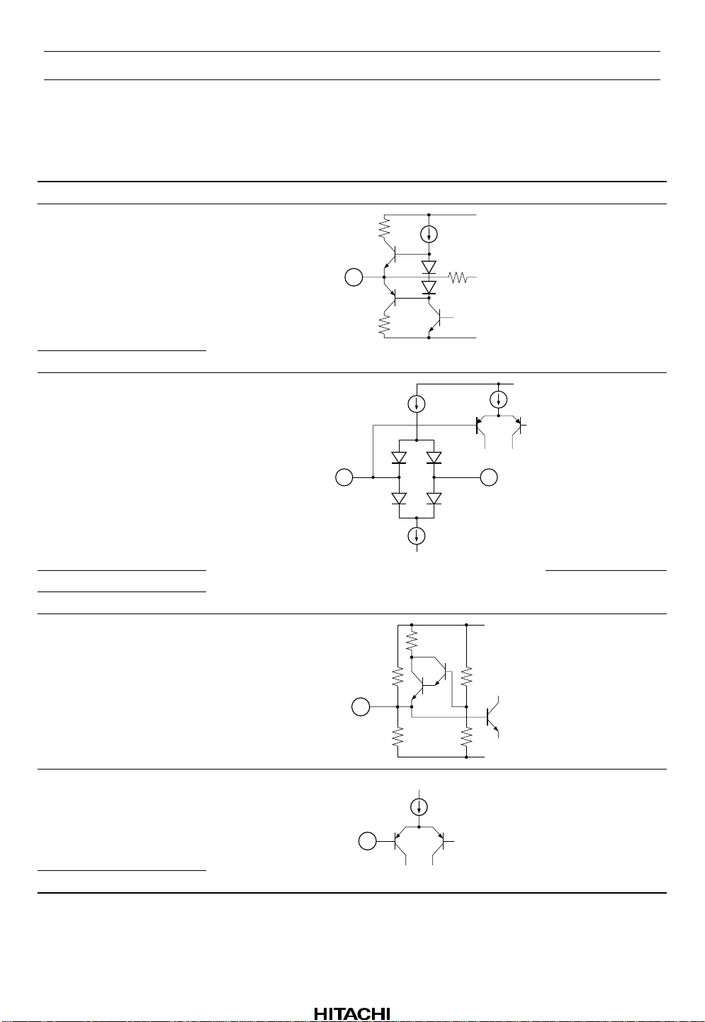
HA12219NT
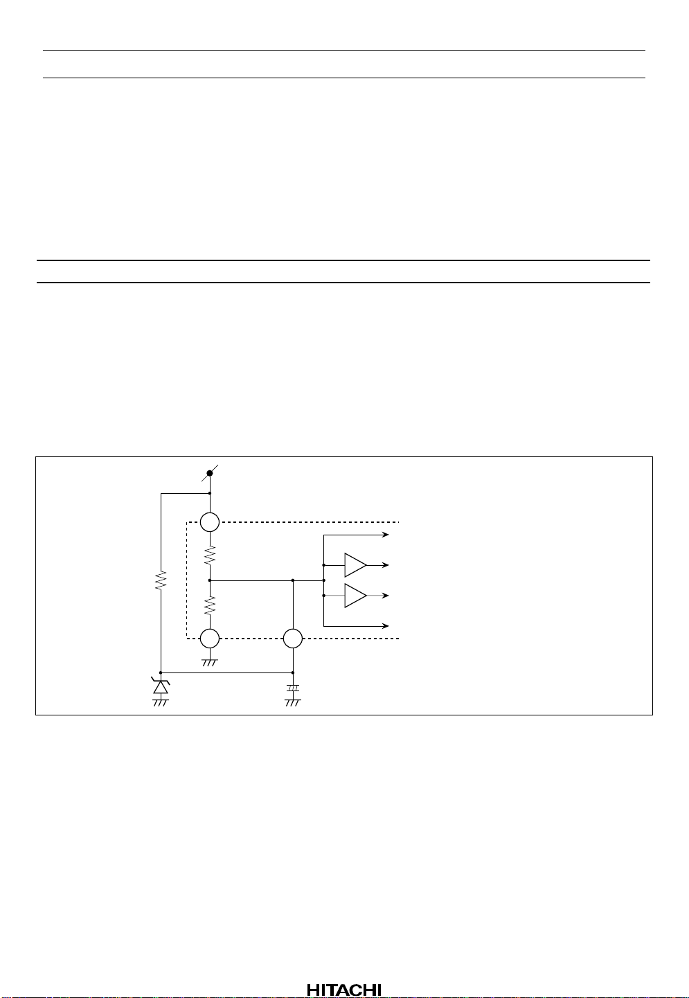
Pin Description, Equivalent Circuit (VCC = 12 V, Vref = 5.6 V, Ta = 25°C, No signal,
The value in the table show typical value.)
Pin No. Pin Name Note Equivalent Circuit Pin Description
1V
CC
V = V
CC
2 REC-OUT(L) V = Vref
3 REC-OUT(R)
4 REC-RETURN V = Vref
V’ = Vref
V
CC
GND
I
,
V4
5 pin, 6 pin
V
VCC pin
REC-EQ output
REC return
V
CC
I
GND
5 PB-IN B(L) PB B deck input
6 PB-IN B(R)
7VREF V = Vref
V’ = V
/ 2
CC
V
CC
Reference
10 k
,
V
V
10 k
GND
8 PB-IN A(L) V = Vref
V
CC
PB A deck input
PB-NF
9 PB-IN A(R)
Rev.2, Jul. 1998, page 2 of 29
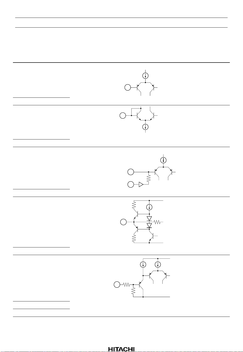
HA12219NT
Pin Description, Equivalent Circuit (VCC = 12 V, Vref = 5.6 V, Ta = 25°C, No signal,
The value in the table show typical value.) (cont)
Pin No. Pin Name Note Equivalent Circuit Pin Description
12 PB-NF(R) PB-IN = Vref
17 PB-NF(L)
13 PB-EQ(R) PB-OUT = Vref
16 PB-EQ(L)
21 REC-IN(R) V = Vref
V
CC
GND
PB-IN
PB-OUT
V
CC
PB-EQ feed back
NAB output
REC-EQ input
22 REC-IN(L)
14 PB-OUT(R) V = Vref
15 PB-OUT(L)
18 A 120/70 I = 20 µA
19 A/B
20 B I/
II
22k
100 k
7Vref
100 k
I
V
CC
GND
V
CC
GND
PB output
Mode control input
Rev.2, Jul. 1998, page 3 of 29
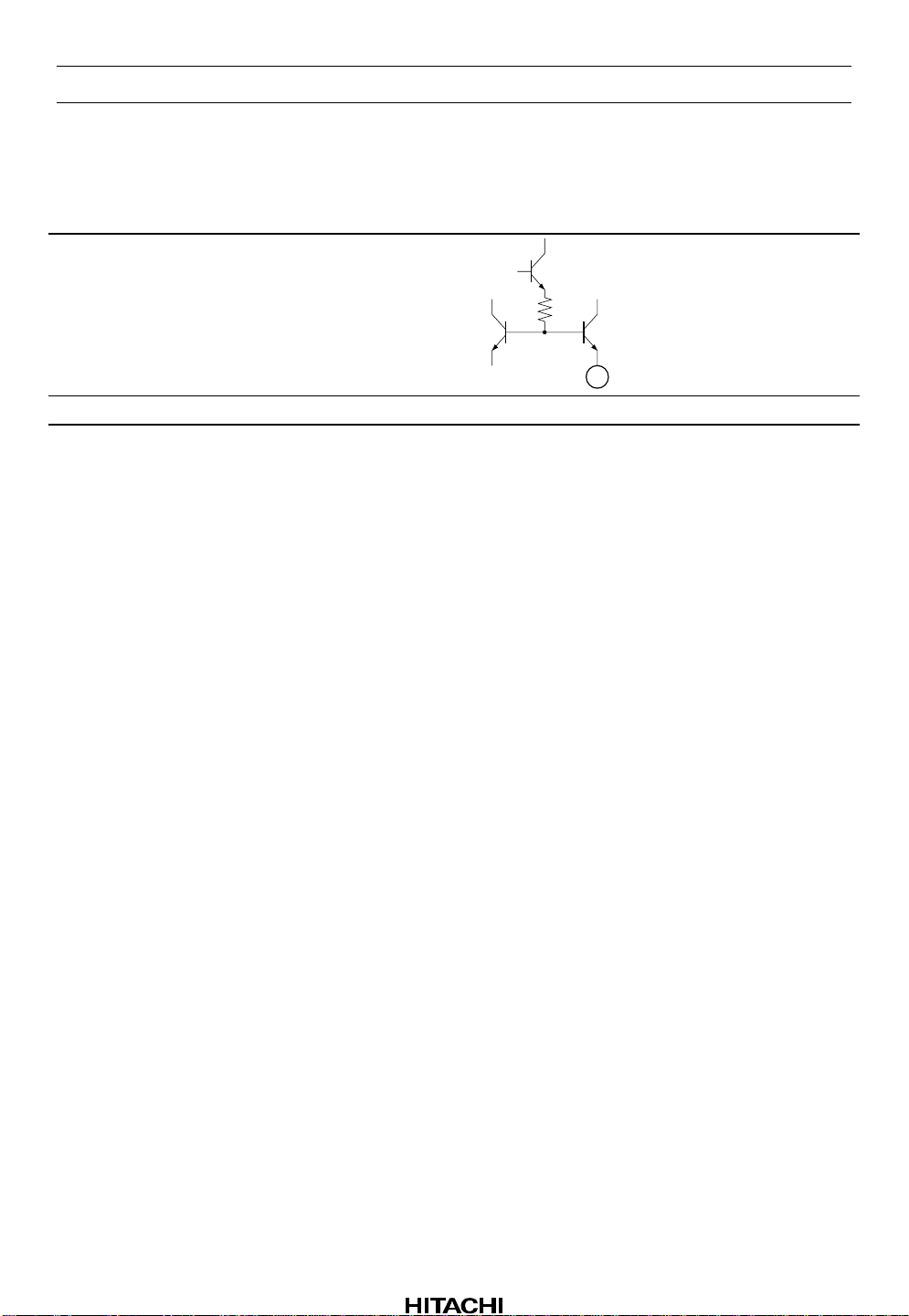
HA12219NT
Pin Description, Equivalent Circuit (VCC = 12 V, Vref = 5.6 V, Ta = 25°C, No signal,
The value in the table show typical value.) (cont)
Pin No. Pin Name Note Equivalent Circuit Pin Description
10 IREF V = 1.2 V
11 GND GND pin
Equalizer
reference current
input
Rev.2, Jul. 1998, page 4 of 29
Block Diagram
HA12219NT
C : F
A /70
A/
13 12
14
17 16 15
18
−
120/70
PB-OUT(R)
PB-OUT(L)
120/70
−
AAB
+
B
GND
Unit R : Ω
IREF
10 11
PB-IN A(R)
PB-IN A(L)
VREF
+
+
PB-IN B(R)
5 6 7 8 9
Return SW
PB-IN B(L)
REC-RETURN
B
/II
20 19
+
(R)
21
+
(L)
22
(R)
REC-IN
(L)
REC-IN
REC-EQ
REC-EQ
(R)
(L)
REC-OUT
REC-OUT
CC
V
1 2 3 4
+ +
CC
V
Rev.2, Jul. 1998, page 5 of 29

HA12219NT
Parallel Data Format
Pin No. Pin Name Lo Mid Hi
18 A 120/70 * — *
19 A/B B
Return SW OFF
REC Mute ON
20 B I/II REC-EQ *
TYPE I
Note: PB-EQ 120/70 logic
A/BBBB
A 120
120/70 B IIII/II Lo Mid Hi
120120
Lo Lo 120 µ 120 µ 120 µ
Lo Hi 70 µ 120 µ 120 µ
Hi Lo 120 µ 70 µ 70 µ
Hi Hi 70 µ 70 µ 70 µ
A
Return SW ON
REC Mute ON
—REC-EQ *
A
Return SW ON
REC Mute OFF
TYPE II
Rev.2, Jul. 1998, page 6 of 29
HA12219NT
Functional Description
Power Supply Range
HA12219NT is designed to operate on single supply, shown by table 1.
Table 1 Supply Voltage
Item Power Supply Range
Single Supply 9.5 V to 15.0 V
Reference Voltage
As AC reference (Vref) of this IC has not a curr ent drivability, Vref fluctuates by A/B switching of PB-EQ.
Provided it causes you anxiety, please supply 7 pin with approximate 1/2 V
For example, a suitable circuit is shown by figure 1.
This IC has a capacitor charger for the Vref, indicated to the pin interface circuit figure.
voltage.
CC
470 Ω
V
CC
1
11
GND
7
Vref
+
470 µF
Figure 1 Reference Voltage Circuit
Lch PB-EQ Reference voltage
Lch REC-EQ Reference voltage
Rch REC-EQ Reference voltage
Rch PB-EQ Reference voltage
Rev.2, Jul. 1998, page 7 of 29
HA12219NT
Operating Mode Control
HA12219NT provides fully electronic switching circuits. And each operating mode control is controlled
by parallel data (DC voltage).
Table 2 shows the control voltage of each control input pin.
Table 2 Control Voltage (Vth)
Pin No. Lo Mid Hi Unit Test Condition
18, 20 0.0 to 0.5 — 2.4 to V
CC
V
Input PinVMeasure
19 0.0 to 0.5 1.2 to 1.8 2.4 to V
CC
V
Note: 1. Each pin is pulled down with 100 kΩ internal resistor. 16 to 18 pins are low-level when each pin
is open.
2. Over shoot level and under shoot level of input signal must be the standardi ze d.
(High: Less than V
, Low: More than –0.2 V)
CC
Block Diagram
Figure 2 shows the block diagram.
As this IC is built-in REC return switch, the configuration system can be simple system using a few
external component and the REC/PB head.
About these logics, please look at the Parallel Data Format.
REC-IN
22
PB-OUT
15
B head
A head
REC-OUT(L)
PB-IN B(L)
PB-IN A(L)
2
4
5
8
Return SW
B
+
−
A
REC - EQ
Vref
Rev.2, Jul. 1998, page 8 of 29
7
Figure 2 Block Diagram (Lch)
1310
Normal Speed
PB-A
HA12219NT
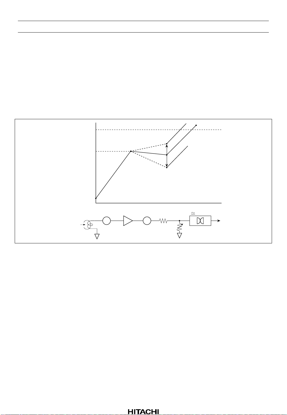
Level Block Diagram
The gain establishment of PB-EQ considers PB output level
{(external AMP+PB AMP <HA12136A>) = 580 mV (Dolby Level)} like figure 3 as the target.
Regarding REC-EQ adjust the gain in front of input to this IC.
Similarly to PB, it consider Dolby level as a stan dard. And R1 needs the value more than 5.6 kΩ.
Because mode establishment resistances are built-in, REC-EQ frequ e n cy characteristics are respectiv ely
fixed value.
In case the change of the frequency characteristics are necessary, please inquire the responsible agent
because the adjustment of resistors is necessary.
580 mV
(Dolby level)
63.6 mV
HA12136A
0.6 mV
40.5 dB
PB-EQ
Figure 3 PB Level Block Diagram (120
Dolby IC
µµµµ
s, 1 kHz)
26 dB
Rev.2, Jul. 1998, page 9 of 29
 Loading...