

HA12232FP
Audio Signal Pre-Amp. for Car Deck
Target Specifications
Description
HA12232FP is audio signal pre-amp. LSI providing PB equalizer op-amp. in one chip.
Function
• PB equalizer × 2 channel
• Vref buffer × 1 channel
ADE-207-328 (Z)
1st Edition
Sep. 2000
Features
• Built-in referential voltage (VREF) for PB equalizer decreases external componen ts.
• This IC is low noise.
• This IC is strong for a cellular phone noise.
Operating Voltage Range
Product Min Max Unit
HA12232FP 6.5 15 V
Note: This IC is designed to operate on single supply.
HA12232FP
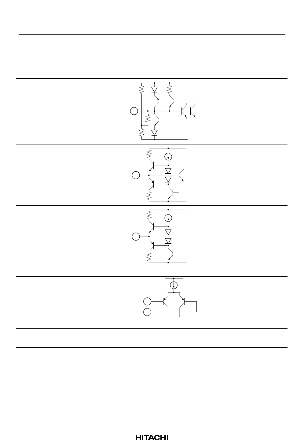
Pin Description, Equivalent Circuit (VCC = 9 V single supply, Ta = 25°C, No Signal,
The value in the table shows typical value.)
Pin No. Pin Name Note Equivalent Circuit Description
7RIP V = V
1VREFV = V
/2
CC
/2
CC
10 EQOUT(L) V = VCC/2
V
V1
V
CC
GND
V
CC
GND
V
CC
Ripple filter
Reference output
Equalizer output
V
GND
5 EQOUT(R)
2 PBIN(R)
PB equalizer input
PBIN
NFI
13 PBIN(L)
3NFI(R)V = V
/2 Equalizer output
CC
12 NFI(L) for time constant
Rev.1, Sep. 2000, page 2 of 14

HA12232FP
Pin Description, Equivalent Circuit (VCC = 9 V single supply, Ta = 25°C, No Signal,
The value in the table shows typical value.) (cont.)
Pin No. Pin Name Note Equivalent Circuit Description
8V
14 GND GND pin
4NC
6
9
11
CC
Power supply
Rev.1, Sep. 2000, page 3 of 14
HA12232FP
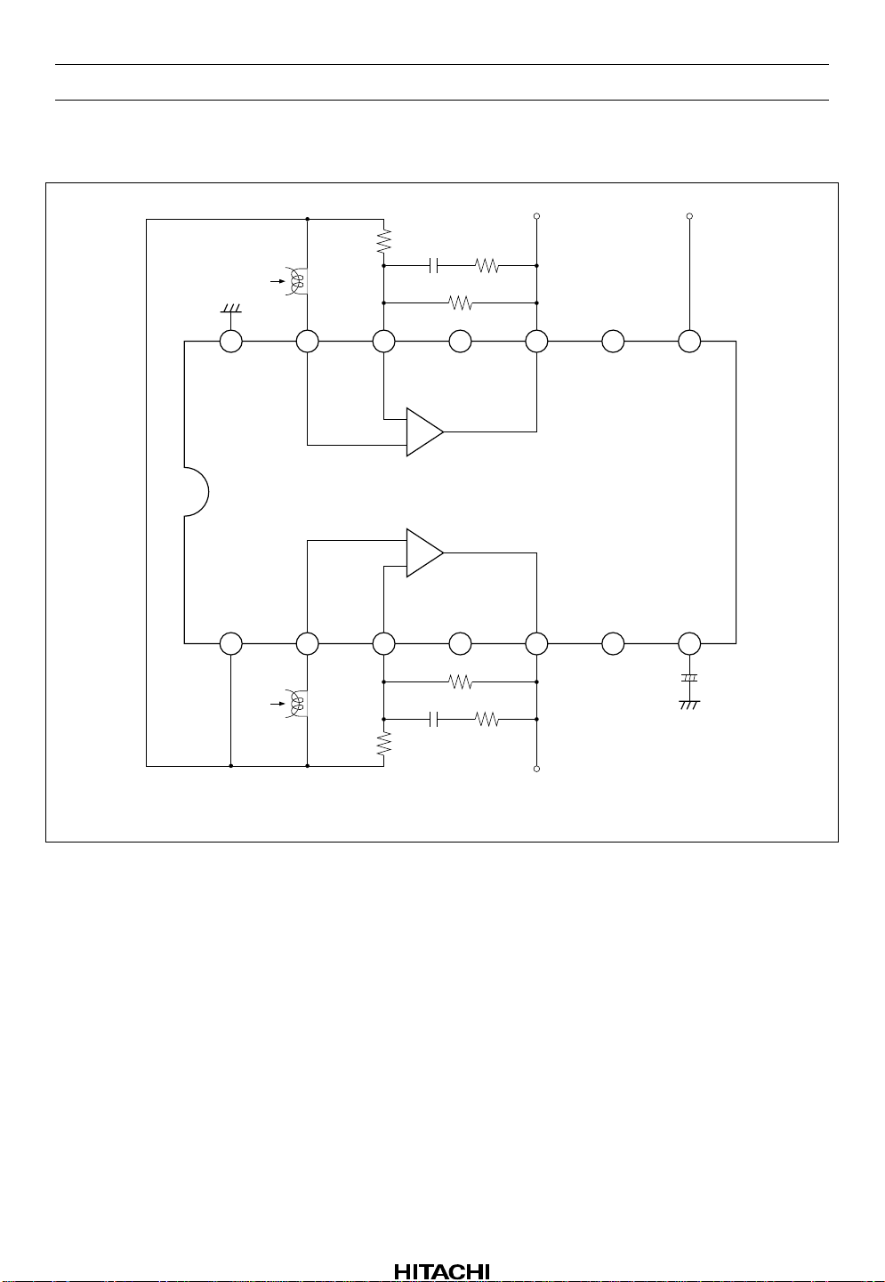
Block Diagram
R6
180
14 13 12 11
GND
PBIN(L)
VREF
1 2 3 4
PBIN(R)
C3
0.01µR412k
R5
330k
NFI(L)
−
+
+
−
NFI(R)
R2
330k
EQOUT(L) V
10
NC
NC
5 6 7
9 8
NC
NC
C2
1µ
CC
RIP
+
R1
180
C1
0.01µ
R3
12k
EQOUT(R)
Unit
R: Ω
C: F
Rev.1, Sep. 2000, page 4 of 14

HA12232FP
Absolute Maximum Ratings (Ta = 25°C)
Item Symbol Rating Unit Note
Supply voltage V
Power dissipation Pd 400 mW Ta ≤ 85°C
Operating temperature Topr −40 to +85 °C
Storage temperature Tstg −55 to +125 °C
Electrical Characteristics (Ta = 25°C, VCC = 9 V, Rg = 680 Ω)
Item Symbol Test Condition Min Typ Max Unit Remark
Quiescent current I
Channel separation CT RL Fin = 1kHz, Vin = 6mVrms 50.0 60.0 dB
EQ gain GV 1k Fin = 1kHz, Vin = 0.6mVrms 37.0 40.0 43.0 dB
THD THD Fin = 1kHz, Vin = 2.4mVrms 0.1 0.5 %
EQ maximum output V
Noise voltage level
converted in input
Note: 1. VCC = 6.5 V
Max 16 V
CC
Specification
Q
No signal 1.5 2.2 3.2 mA
GV 10k Fin = 10kHz, Vin = 0.6mVrms 33.0 36.0 39.0 dB
OM
Fin = 1kHz, THD = 1% 300 600 mVrms *1
VN Rg = 680Ω, Din-Audio Filter 0.7 1.5 µVrms
Rev.1, Sep. 2000, page 5 of 14

HA12232FP
Functional Description
Power Supply Range
HA12232FP is designed to operate on single supply only.
Table 1 Supply Voltage Range
Product Single Supply
HA12232FP 6.5 V to 15.0 V
Reference Voltage
HA12232FP provides the reference voltage of half the supply voltage that is the signal grounds. As the
peculiarity of this device, the capacitor for the ripple filter is very small ab out 1 /1 00 compared with their
usual value. The block diagram is shown as figure 1.
8V
CC
+
−
14
7
1
Figure 1 The Block Diagram of Reference Supply Voltage
Rev.1, Sep. 2000, page 6 of 14

Input Block Diagram and Lev e l Diagram
Vref
HA12232FP
0.6mVrms
(−62.2dBs)
PBIN
Figure 2 Input Block Diagram
Cutoff Frequency, Gain of PB-EQ Amp.
G
0
60mVrms
+
−
PB-EQ
(−22.2dBs)
EQOUT
Amp.
NFI
R2
330k
R1
180
C1
0.01µ
R3
12k
PB-EQ Amp. Gv = 40 dB, f = 1 kHz
Transfer Function
2
[w2 c
T = R
+ j ⋅ R2w c
2
(R2 + R3) (R1 + R3) + 1] / R1 [w2 c
1
2
(R1 − R2) / R1 [w2 c
1
2
(R2 + R3)2 + 1]
1
2
(R2 + R3)2 + 1]
1
Cutoff Frequency
2
1/2
G
V
fc = {[−b ± (b
a = 2c
G
∞
b = [3 (R2 + R3) (R3 + R1) − (R2 + R3)2 − (R3 + R1)2] c
− 4a)
4
(R2 + R3)2 (R3 + R1)
1
] / 2a} / 2π
2
2
1
Changing the value of each element to one shown in figure 2,
will be as follows.
fc1 fc2
f
fc1 = 50 Hz, fc2 = 1300 Hz
PB-EQ Amp. Gain (f = 0, ∞)
f = 0
= R2 / R
T
0
1
G0 = 65.3 dB
f = ∞
T
= R2 (R3 + R1) / R1 (R2 + R3)
∞
G
= 36.3 dB
∞
Figure 3 Cutoff Frequency of PB-EQ Amp.
Rev.1, Sep. 2000, page 7 of 14

HA12232FP
Test Circuit
DC +9V
SOURCE1
+
C6
100µ
CC
DC VM1
SW3
Lch
Rch
Noise
meter
Oscillo
Distortion
analyzer
SW2SW1
Lch
Rch
scope
RIP
+
C2
1µ
AC VM2
V
R10
10k
C8
−
NC
EQOUT(R)
5 6 7
NC
R2
NFI(R)
PBIN(R)
2 3 4
VREF
1
330k
+
R7
C4
R3
C1
R1
680
22µ
12k
0.01µ
180
+
C7
R9
10k
2.2µ
2. Capacitor tolerance ±1%
3. Unit R: Ω, C: F
NC
9 8
NC
NFI(L)
GND
EQOUT(L)
−
+
PBIN(L)
Lch
+
Rch
+
2.2µ
R4
12k
C3
0.01µ
R6
180
R8
680
+
C5
22µ
R5
10
330k
14 13 12 11
Rev.1, Sep. 2000, page 8 of 14
AC VM1
AUDIO SG
Notes: 1. Resistor tolerance ±1%

Characteristic Curves
HA12232FP
−40
3.0
2.5
(mA)
Q
2.0
Quiescent Current I
1.5
5 6 14 15131211 1610987
Quiescent Current vs. Supply Voltage
Channel Separation vs. Frequency (L→R, R→L)
Supply Voltage (V)
−60
−80
−100
Channel Separation (dB)
−120
−140
10 100 100k10k1k
Frequency (Hz)
Rev.1, Sep. 2000, page 9 of 14

HA12232FP
80
70
60
50
EQ Gain (dB)
40
30
VCC = 9.0 V
PBIN→EQOUT
20
10 100k10k1k100
1.0
EQ Amp. Gain vs. Frequency
Frequency (Hz)
Total Harmonic Distortion vs. Supply Voltage
100 Hz (30 kHz LPF)
1 kHz (400 Hz HPF + 30 kHz LPF)
10 kHz (400 Hz HPF + 80 kHz LPF)
PBIN→EQOUT
Vout = 240 mVrms
0.1
T.H.D. (%)
0.01
0.001
56 14131211 161510987
Rev.1, Sep. 2000, page 10 of 14
Supply Voltage (V)

HA12232FP
10.0
PBIN→EQOUT
V
1.0
0 dB = 60 mVrms
0.1
T.H.D. (%)
0.01
0.001
5.0
PBIN→EQOUT
T.H.D. ≅ 1 %
4.0
Total Harmonic Distortion vs. Output Level
100 Hz (30 kHz LPF)
1 kHz (400 Hz HPF + 30 kHz LPF)
10 kHz (400 Hz HPF + 80 kHz LPF)
= 9.0 V
CC
10 20 30−10 0
Output Level Vout (dB)
Signal Handling
100 Hz (30 kHz LPF)
1 kHz (400 Hz HPF + 30 kHz LPF)
10 kHz (400 Hz HPF + 80 kHz LPF)
40
3.0
Vomax (Vrms)
2.0
1.0
56 14131211 161510987
Supply Voltage (V)
Rev.1, Sep. 2000, page 11 of 14

HA12232FP
Noise Voltage Level Converted in Input vs. Supply Voltage
1.5
Rg = 680 Ω
Din-Audio Filter
1.0
0.5
Noise Voltage Level Converted in Input (µVrms)
0
56 14131211 161510987
Supply Voltage (V)
20
Ripple Rejection Ratio vs. Frequency
0
−20
−40
Ripple Rejection Ratio R.R.R. (dB)
−60
10 100 100k10k1k
Frequency (Hz)
Rev.1, Sep. 2000, page 12 of 14

Package Dimensions
14
1
1.27
10.06
10.5 Max
1.42 Max
HA12232FP
Unit: mm
8
5.5
7
+ 0.20
7.80
– 0.30
2.20 Max
*0.22 ± 0.05
1.15
0.20 ± 0.04
0˚ – 8˚
0.70 ± 0.20
*0.42 ± 0.08
0.40 ± 0.06
*Dimension including the plating thickness
Base material dimension
0.10 ± 0.10
0.15
0.12
M
Hitachi Code
JEDEC
EIAJ
Mass
(reference value)
FP-14DA
—
Conforms
0.23 g
Rev.1, Sep. 2000, page 13 of 14

HA12232FP
Disclaimer
1. Hitachi neither warrants nor grants licenses of any rights of Hitachi’s or any third party’s patent,
copyright, trademark, or other intellectual property rights for information contained in this document.
Hitachi bears no responsibility for problems that may arise with third party’s rights, in cluding
intellectual property rights, in connection with u se of the information contained in this document.
2. Products and product specifications may be subject to change without notice. Confirm that you have
received the latest product standards or specifications before final design, purchase or use.
3. Hitachi makes every attempt to ensure that its products are of high quality and reliability. However,
contact Hitachi’s sales office before using the product in an application that demands especially high
quality and reliability or where its failure or malfunction may directly threaten human life or cause risk
of bodily injury, such as aerospace, aeronautics, nuclear power, combustion control, transportation,
traffic, safety equipment or medical equipment for life support.
4. Design your application so that the product is used within the ranges guaranteed by Hitachi particularly
for maximum rating, operating supply voltage range, heat radiation characteristics, installation
conditions and other characteristics. Hitachi bears no responsibility for failure or damage when used
beyond the guaranteed ranges. Even within the guaranteed ranges, consider normally foreseeable
failure rates or failure modes in semiconductor devices and employ systemic measures such as failsafes, so that the equipment incorporating Hitachi product does not cause bodily injury, fire or other
consequential damage due to operation of the Hitachi product.
5. This product is not designed to be radiation resistant.
6. No one is permitted to reproduce or duplicate, in any form, the whole or part of this document without
written approval from Hitachi.
7. Contact Hitachi’s sales office for any questions regarding this document or Hitachi semiconductor
products.
Sales Offices
Hitachi, Ltd.
Semiconductor & Integrated Circuits.
Nippon Bldg., 2-6-2, Ohte-machi, Chiyoda-ku, Tokyo 100-0004, Japan
Tel: Tokyo (03) 3270-2111 Fax: (03) 3270-5109
URL NorthAmerica : http://semiconductor.hitachi.com/
For further information write to:
Hitachi Semiconductor
(America) Inc.
179 East Tasman Drive,
San Jose,CA 95134
Tel: <1> (408) 433-1990
Fax: <1>(408) 433-0223
Europe : http://www.hitachi-eu.com/hel/ecg
Asia : http://sicapac.hitachi-asia.com
Japan : http://www.hitachi.co.jp/Sicd/indx.htm
Hitachi Europe GmbH
Electronic Components Group
Dornacher Straße 3
D-85622 Feldkirchen, Munich
Germany
Tel: <49> (89) 9 9180-0
Fax: <49> (89) 9 29 30 00
Hitachi Europe Ltd.
Electronic Components Group.
Whitebrook Park
Lower Cookham Road
Maidenhead
Berkshire SL6 8YA, United Kingdom
Tel: <44> (1628) 585000
Fax: <44> (1628) 585160
Hitachi Asia Ltd.
Hitachi Tower
16 Collyer Quay #20-00,
Singapore 049318
Tel : <65>-538-6533/538-8577
Fax : <65>-538-6933/538-3877
URL : http://www.hitachi.com.sg
Hitachi Asia Ltd.
(Taipei Branch Office)
4/F, No. 167, Tun Hwa North Road,
Hung-Kuo Building,
Taipei (105), Taiwan
Tel : <886>-(2)-2718-3666
Fax : <886>-(2)-2718-8180
Telex : 23222 HAS-TP
URL : http://www.hitachi.com.tw
Copyright Hitachi, Ltd., 2000. All rights reserved. Printed in Japan.
Hitachi Asia (Hong Kong) Ltd.
Group III (Electronic Components)
7/F., North Tower,
World Finance Centre,
Harbour City, Canton Road
Tsim Sha Tsui, Kowloon,
Hong Kong
Tel : <852>-(2)-735-9218
Fax : <852>-(2)-730-0281
URL : http://www.hitachi.com.hk
Colophon 2.0
Rev.1, Sep. 2000, page 14 of 14
 Loading...