

Page 1

81
AVR3550HD harman/kardon
1.1 Features
9. 8bit Serial Expansion Interface (SEI): 1 channel
(MSB/LSB selectable and max. 4Mbps at 16MHz)
10. 10-bit successive approximation type AD converter
- Analog input: 6 ch
11. Key-on wakeup : 4 channels
12. Clock operation
Single clock mode
Dual clock mode
13. Low power consumption operation
STOP mode: Oscillation stops. (Battery/Capacitor back-up.)
SLOW1 mode: Low power consumption operation using low-frequency clock.(High-frequency clock
stop.)
SLOW2 mode: Low power consumption operation using low-frequency clock.(High-frequency clock
oscillate.)
TMP86F409NG
IDLE0 mode: CPU stops, and only the Time-Based-Timer(TBT) on peripherals operate using high fre-
quency clock. Release by falling edge of the source clock which is set by TBTCR<TBTCK>.
IDLE1 mode: CPU stops and peripherals operate using high frequency clock. Release by interru-
puts(CPU restarts).
IDLE2 mode: CPU stops and peripherals operate using high and low frequency clock. Release by inter-
ruputs. (CPU restarts).
SLEEP0 mode: CPU stops, and only the Time-Based-Timer(TBT) on peripherals operate using low fre-
quency clock.Release by falling edge of the source clock which is set by TBTCR<TBTCK>.
SLEEP1 mode: CPU stops, and peripherals operate using low frequency clock. Release by interru-
put.(CPU restarts).
SLEEP2 mode: CPU stops and peripherals operate using high and low frequency clock. Release by
interruput.
14. Wide operation voltage:
4.5 V to 5.5 V at 16MHz /32.768 kHz
2.7 V to 5.5 V at 8 MHz /32.768 kHz
Page 2
82
AVR3550HD harman/kardon
TMP86F409NG
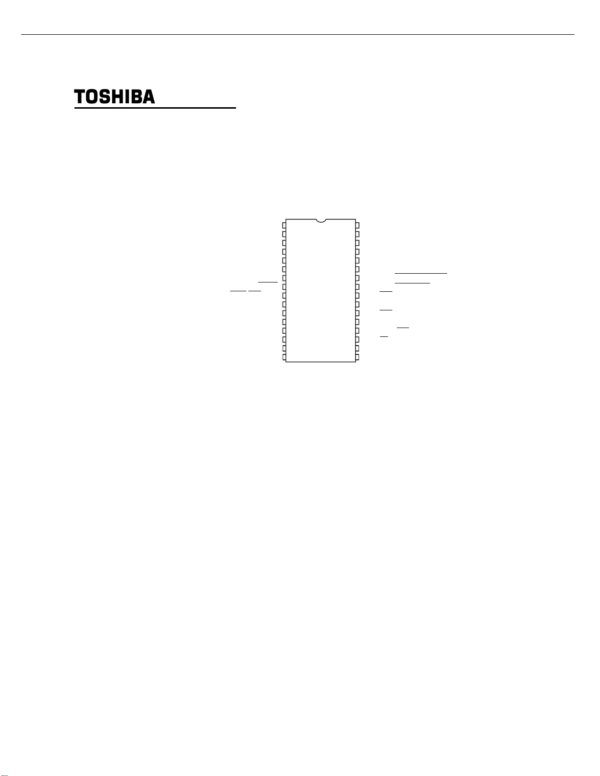
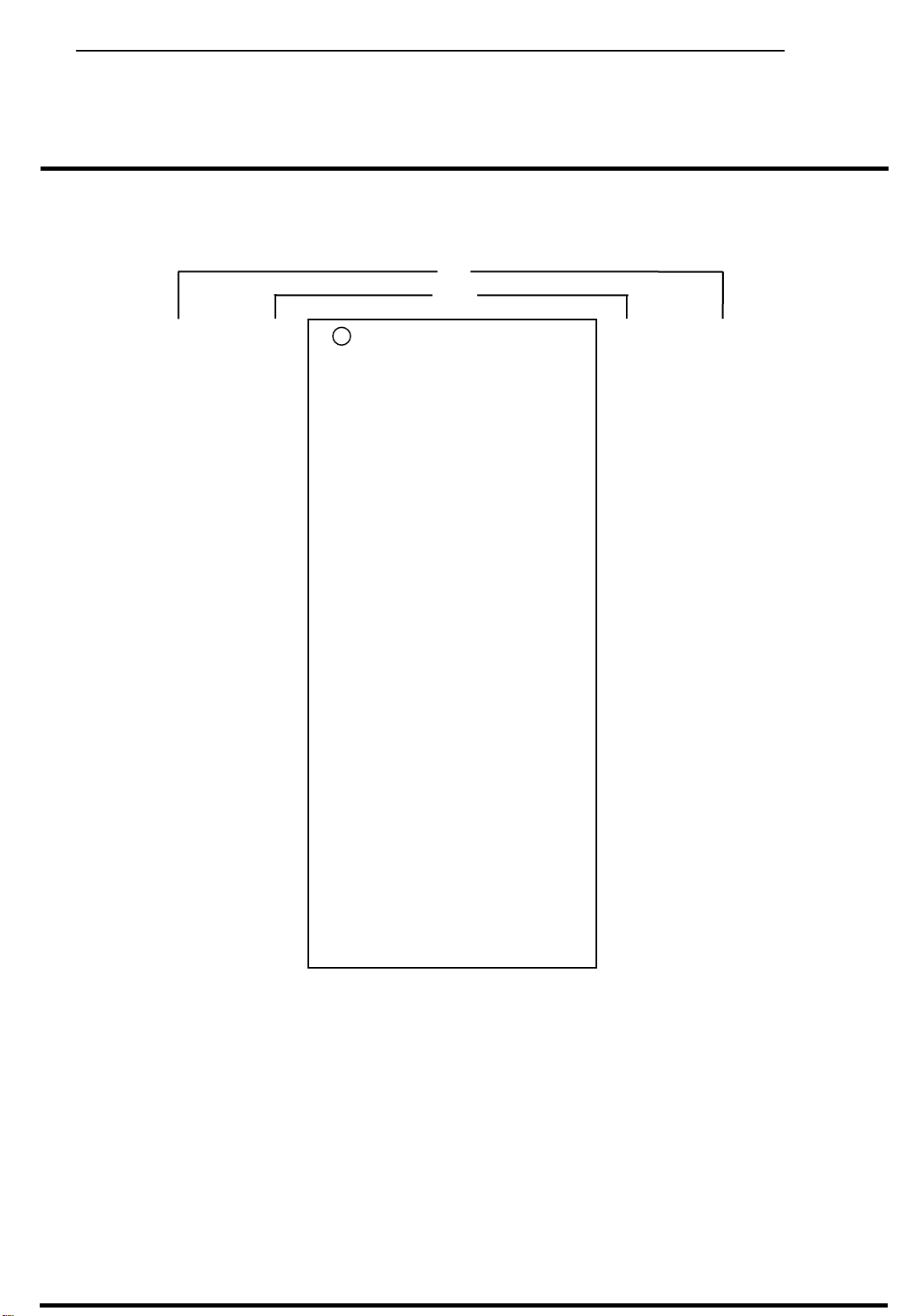
1.2 Pin Assignment
VSS
XIN
XO
UT
TEST
VDD
(XTIN) P21
(XTOUT) P22
RESET
(STOP/INT5) P20
(TX
D) P00
(RXD) P01
(SCLK) P02
(MOSI) P03
(MISO) P04
P14
P16
1
2
3
4
5
6
7
8
9
10
11
12
13
14
15
16
P37 (AIN5/STOP5)
32
P36 (AIN4/STOP4)
31
P35 (AIN3/STOP3)
30
P34 (AIN2/STOP2)
29
P33 (AIN1)
28
P
32 (AIN0)
27
P31 (TC4/PDO4/PWM4/PPG4)
26
P30 (TC3/PDO3/PWM3
25
24
23
22
21
20
19
18
17
DVO)
P12 (
P11 (INT1)
INT0)
P10 (
P07 (TC1/INT4)
P06 (INT3/PPG)
P05 (SS)
P13
P15
)
Figure 1-1 Pin Assignment
Page 3
83
AVR3550HD harman/kardon
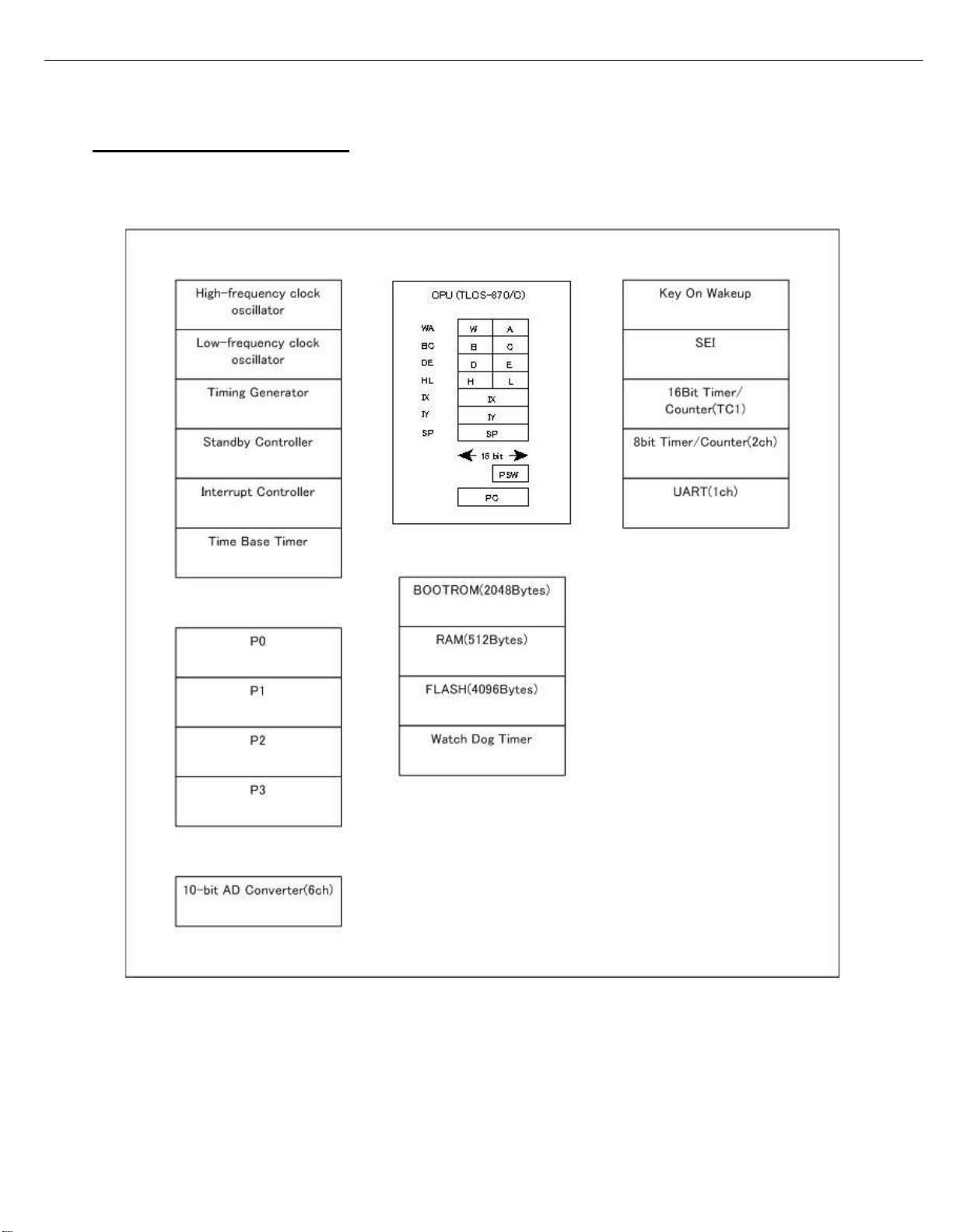
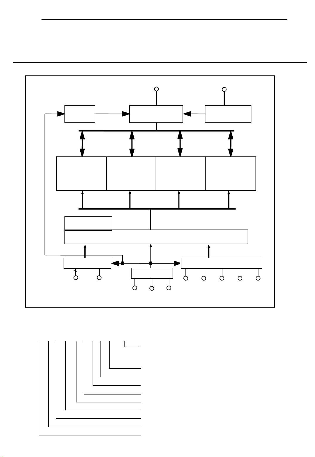
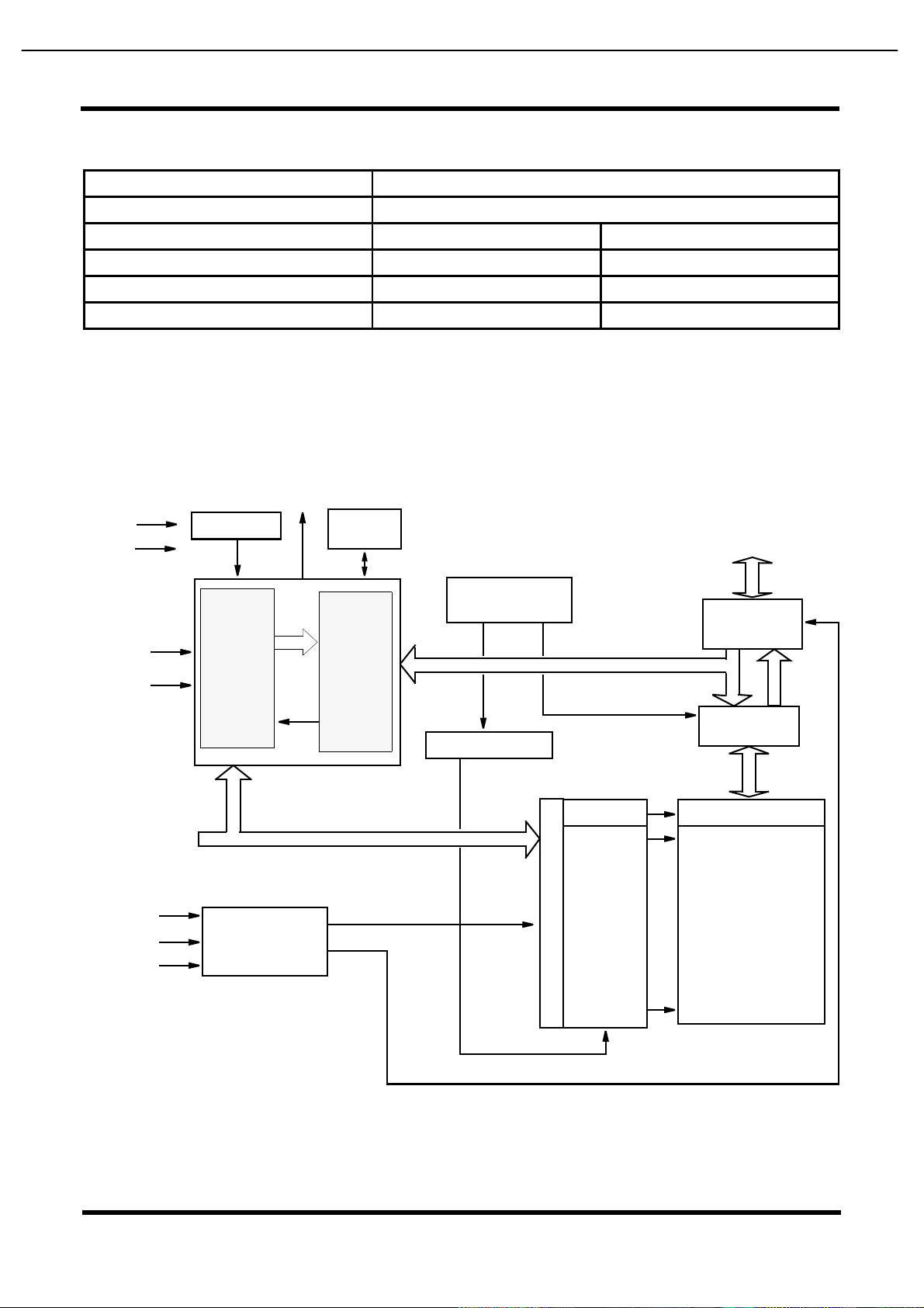
1.3 Block Diagram
TMP86F409NG
1.3 Block Diagram
Figure 1-2 Block Diagram
Page 4
84
AVR3550HD harman/kardon
TMP86F409NG
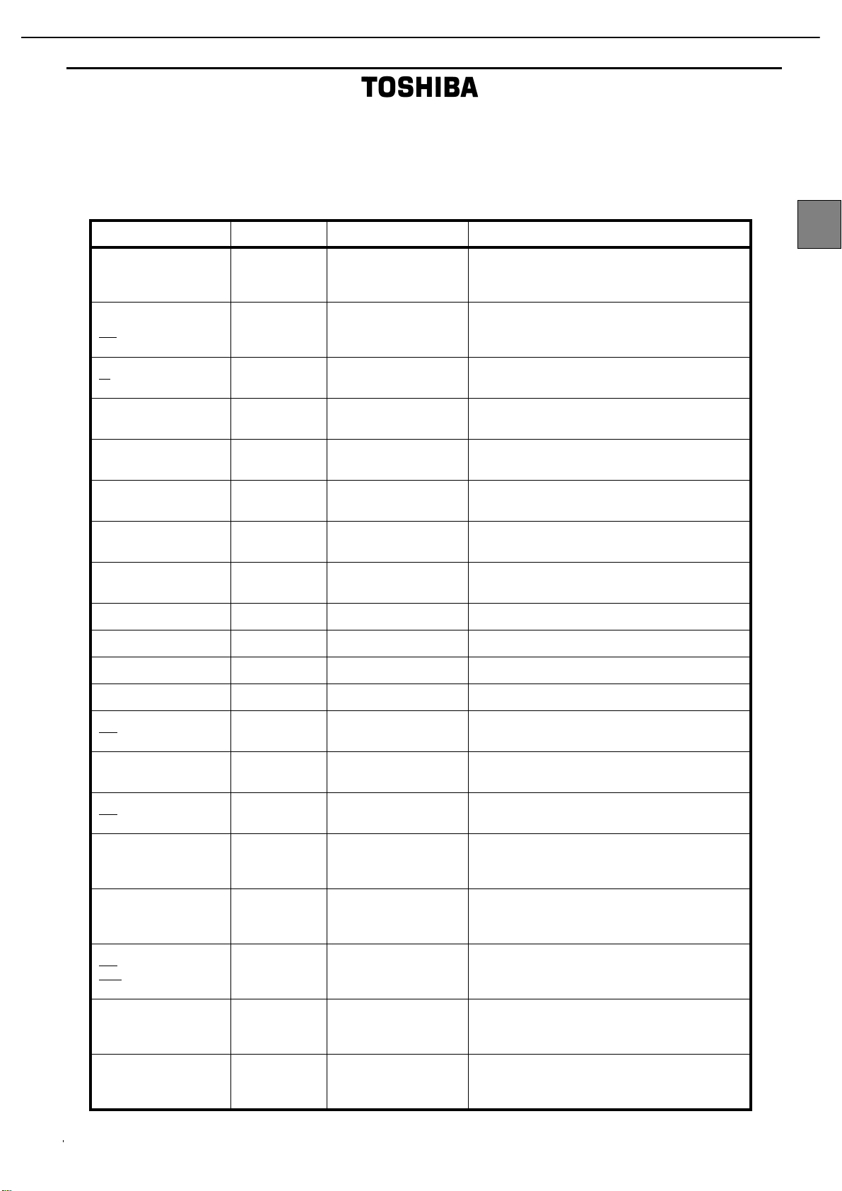
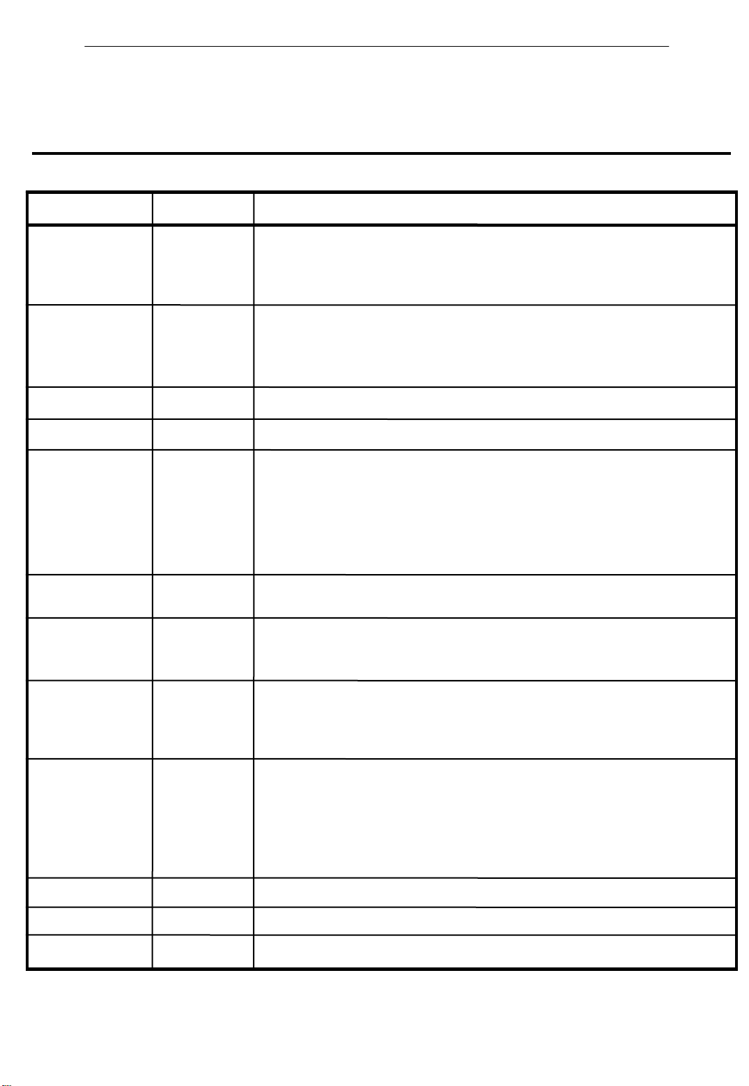
1.4 Pin Names and Functions
The TMP86F409NG has MCU mode, parallel PROM mode, and serial PROM mode. Table 1-1 shows the pin
functions in MCU mode. The serial PROM mode is explained later in a separate chapter.
Table 1-1 Pin Names and Functions(1/2)
Pin Name Pin Number Input/Output Functions
P07
TC1
INT4
P06
INT3
PPG
P05
SS
P04
MISO
P03
MOSI
P02
SCLK
P01
RXD
P00
TXD
P16 16 IO PORT16
P15 17 IO PORT15
P14 15 IO PORT14
21
20
19
14
13
12
11
10
IO
PORT07
I
TC1 input
I
External interrupt 4 input
PORT06
IO
I
External interrupt 3 input
PPG output
O
IOIPORT05
SEI master/slave select input
IOIOPORT04
SEI master input, slave output
IOIOPORT03
SEI master input, slave output
IOIOPORT02
SEI serial clock input/output pin
IOIPORT01
UART data input
IOOPORT00
UART data output
P13 18 IO PORT13
P12
DVO
P11
INT1
P10
INT0
P22
XTOUT
P21
XTIN
P20
INT5
STOP
P37
AIN5
STOP5
P36
AIN4
STOP4
24
23
22
7
6
9
32
31
IOOPORT12
Divider Output
IOIPORT11
External interrupt 1 input
IOIPORT10
External interrupt 0 input
PORT22
IO
Resonator connecting pins(32.768kHz) for inputting external
O
clock
PORT21
IO
Resonator connecting pins(32.768kHz) for inputting external
I
clock
IO
PORT20
I
External interrupt 5 input
I
STOP mode release signal input
IO
PORT37
I
Analog Input5
I
STOP5
IO
PORT36
I
Analog Input4
I
STOP4
Page 5
85
AVR3550HD harman/kardon
TMP86F409NG
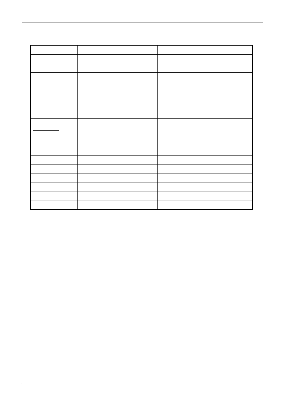
Table 1-1 Pin Names and Functions(2/2)
Pin Name Pin Number Input/Output Functions
P35
AIN3
STOP3
P34
AIN2
STOP2
P33
AIN1
P32
AIN0
P31
TC4
PDO4/PWM4/PPG4
P30
TC3
PDO3/PWM3
XIN 2 I Resonator connecting pins for high-frequency clock
XOUT 3 O Resonator connecting pins for high-frequency clock
RESET 8 I Reset signal
TEST 4 I Test pin for out-going test. Normally, be fixed to low.
30
29
28
27
26
25
IO
PORT35
I
Analog Input3
I
STOP3
IO
PORT34
I
Analog Input2
I
STOP2
IOIPORT33
Analog Input1
IOIPORT32
Analog Input0
IO
PORT31
I
TC4 input
O
PDO4/PWM4/PPG4 output
IO
PORT30
I
TC3 input
O
PDO3/PWM3 output
VDD 5 I +5V
VSS 1 I 0(GND)
Page 6
86
AVR3550HD harman/kardon
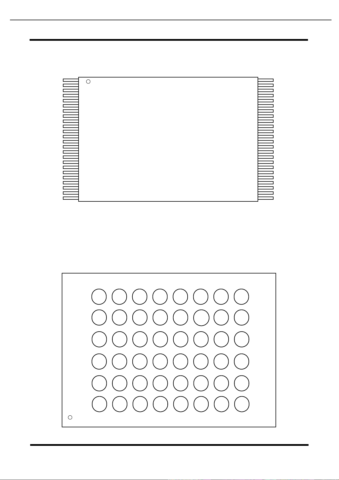
A3S56D30ETP
A3S56D40ETP
256M Double Data Rate Synchronous DRAM
Pin Assignment (Top View) 66-pin TSOP
x8
x16
VDD
DQ0
VDDQ
NC
DQ1
VSSQ
NC
DQ2
VDDQ
NC
DQ3
VSSQ
NC
NC
VDDQ
NC
NC
VDD
NC
NC
/WE
/CAS
/RAS
/CS
NC
BA0
BA1
A10/AP
A0
A1
A2
A3
VDD
VDD
DQ0
VDDQ
DQ1
DQ2
VSSQ
DQ3
DQ4
VDDQ
DQ5
DQ6
VSSQ
DQ7
NC
VDDQ
LDQS
NC
VDD
NC
LDM
/WE
/CAS
/RAS
/CS
NC
BA0
BA1
A10/AP
A0
A1
A2
A3
VDD
1
2
3
4
5
6
7
8
9
10
11
12
13
14
15
16
17
18
19
20
21
22
23
24
25
26
27
28
29
30
31
32
33
66pin TSOP(II)
400mil width
x
875mil length
0.65mm
Lead Pitch
Row
A0-12
Column
A0-9 (x8)
A0-8 (x16)
66
65
64
63
62
61
60
59
58
57
56
55
54
53
52
51
50
49
48
47
46
45
44
43
42
41
40
39
38
37
36
35
34
VSS
DQ15
VSSQ
DQ14
DQ13
VDDQ
DQ12
DQ11
VSSQ
DQ10
DQ9
VDDQ
DQ8
NC
VSSQ
UDQS
NC
VREF
VSS
UDM
/CLK
CLK
CKE
NC
A12
A11
A9
A8
A7
A6
A5
A4
VSS
VSS
DQ7
VSSQ
NC
DQ6
VDDQ
NC
DQ5
VSSQ
NC
DQ4
VDDQ
NC
NC
VSSQ
DQS
NC
VREF
VSS
DM
/CLK
CLK
CKE
NC
A12
A11
A9
A8
A7
A6
A5
A4
VSS
CLK, /CLK
CKE
/CS
/RAS
/CAS
/WE
DQ0-15
DQ0-7
UDM, LDM
DM
UDQS, LDQS
DQS
: Master Clock
: Clock Enable
: Chip Select
: Row Address Strobe
: Column Address Strobe
: Write Enable
: Data I/O (x16)
: Data I/O (x8)
: Write Mask (x16)
: Write Mask (x8)
: Data Strobe (x16)
: Data Strobe (x8)
A0-12
BA0,1
Vdd
VddQ
Vss
VssQ
: Address Input
: Bank Address Input
: Power Supply
: Power Supply for Output
: Ground
: Ground for Output
Page 7
87
AVR3550HD harman/kardon
256M Double Data Rate Synchronous DRAM
PIN FUNCTION
SYMBOL TYPE DESCRIPTION
Clock: CLK and /CLK are differential clock inputs. All address and control
input signals are sampled on the crossing of the positive edge of CLK and
CLK, /CLK Input
CKE Input
/CS Input Chip Select: When /CS is high, any command means No Operation.
/RAS, /CAS, /WE Input Combination of /RAS, /CAS, /WE defines basic commands.
negative edge of /CLK. Output (read) data is referenced to the crossings of
CLK and /CLK (both directions of crossing).
Clock Enable: CKE controls internal clock. When CKE is low, internal clock
for the following cycle is ceased. CKE is also used to select auto / self refresh.
After self refresh mode is started, CKE becomes asynchronous input. Self refresh
is maintained as long as CKE is low.
A3S56D30ETP
A3S56D40ETP
A0-12 Input
BA0,1 Input
DQ0-7 (x8),
DQ0-15 (x16),
DQS (x8)
UDQS, LDQS (x16)
DM (x8)
UDM, LDM (x16)
Input / Output
Input / Output
Input
A0-12 specify the Row / Column Address in conjunction with BA0,1. The
Row Address is specified by A0-12. The Column Address is specified by
A0-9(x8) and A0-8(x16). A10 is also used to indicate precharge
option. When A10 is high at a read / write command, an auto precharge is
performed. When A10 is high at a precharge command, all banks are
precharged.
Bank Address: BA0,1 specifies one of four banks to which a command is
applied. BA0,1 must be set with ACT, PRE, READ, WRITE commands.
Data Input/Output: Data bus
Data Strobe: Output with read data, input with write data. Edge-aligned
with read data, centered in write data. Used to capture write data.
For the x16, LDQS corresponds to the data on DQ0-DQ7; UDQS
correspond to the data on DQ8-DQ15
Input Data Mask: DM is an input mask signal for write data. Input data
is masked when DM is sampled HIGH along with that input data
during a WRITE access. DM is sampled on both edges of DQS.
Although DM pins are input only, the DM loading matches the DQ
and DQS loading. For the x16, LDM corresponds to the data on DQ0-DQ7;
UDM corresponds to the data on DQ8-DQ15.
Vdd, Vss Power Supply Power Supply for the memory array and peripheral circuitry.
VddQ, VssQ Power Supply VddQ and VssQ are supplied to the Output Buffers only.
Vref Input SSTL_2 reference voltage.
Page 8
88
AVR3550HD harman/kardon
A3S56D30ETP
A3S56D40ETP
256M Double Data Rate Synchronous DRAM
BLOCK DIAGRAM
A3S56D30ETP
DLL
Memory
Array
Bank #0
Mode Register
I/O Buffer
Memory
Array
Bank #1
Control Circuitry
DQ0 - 7
Memory
Array
Bank #2
DQS
DQS
Memory
Bank #3
Buffer
Array
Address Buffer
A0-12
BA0,1
Type Designation Code
A 3 S 56 D 3 0 E TP –G5
Control Signal Buffer
Clock Buffer
/CS /RAS /CAS /WE DM
/CLK
CLK CKE
This rule is applied to only Synchronous DRAM family.
Speed Grade
Package Type TP: TSOP(II)
Process Generation
Function Reserved for Future Use
Organization 2n3: x8
DDR Synchronous DRAM
Density 56: 256M bits
Interface S:SSTL_3, _2
Memory Style (DRAM)
Zentel DRAM
6: 166MHz @CL=3.0/2.5, and 133MHz @CL=2.0
5: 200MHz @CL=3.0, 166MHz @CL=2.5, and 133MHz @CL=2.0
5E: 200MHz @CL=3.0/2.5, and 133MHz @CL=2.0
Page 9
89
AVR3550HD harman/kardon
A3S56D30ETP
A3S56D40ETP
256M Double Data Rate Synchronous DRAM
BLOCK DIAGRAM
A3S56D40ETP
DLL
Memory
Array
Bank #0
Mode Register
I/O Buffer
Memory
Array
Bank #1
Control Circuitry
DQ0 - 15
Memory
Array
Bank #2
UDQS, LDQS
DQS Buffer
Memory
Array
Bank #3
Address Buffer
A0-12
BA0,1
Type Designation Code
A 3 S 56 D 4 0 E TP –G5
Control Signal Buffer
Clock Buffer
/CS /RAS /CAS /WE UDM,
/CLK
CLK CKE
This rule is applied to only Synchronous DRAM family.
Speed Grade
Package Type TP: TSOP(II)
Process Generation
Function Reserved for Future Use
Organization 2n4: x16
DDR Synchronous DRAM
Density 56: 256M bits
Interface S:SSTL_3, _2
Memory Style (DRAM)
Zentel DRAM
6: 166MHz @CL=3.0/2.5, and 133MHz @CL=2.0
5: 200MHz @CL=3.0, 166MHz @CL=2.5, and 133MHz @CL=2.0
5E: 200MHz @CL=3.0/2.5, and 133MHz @CL=2.0
LDM
Page 10

90
AVR3550HD harman/kardon
Excel Semiconductor inc.
ES29LV320E
32Mbit(4M x 8/2M x 16)
CMOS 3.0 Volt-only, Boot Sector Flash Memory
GENERAL FEATURES
• Single power supply operation
- 2.7V ~ 3.6V for read, program and erase operations
•Sector Structure
- 8Kbyte x 8 boot sectors
- 64Kbyte x 63 sectors
- 256byte security sector
• Top or Bottom boot block
- ES29LV320ET for Top boot block device
- ES29LV320EB for Bottom boot block device
• A 256 bytes of extra sector for security code
- Factory locked
- Customer lockable
• Package Options
- 48-pin TSOP
- 48-ball FBGA
- Pb-free packages
- All Pb-free products are RoHS-Compliant
• Low Vcc write inhibit
• Manufactured on 0.18um process technology
• Compatible with JEDEC standards
- Pinout and software compatible with single-power
supply flash standard
DEVICE PERFORMANCE
• Read access time
- 70ns/90ns for normal Vcc range ( 2.7V ~ 3.6V )
• Program and erase time
- Program time : 6us/byte, 8us/word ( typical )
- Accelerated program time : 4us/word ( typical )
- Sector erase time : 0.7sec/sector ( typical )
• Power consumption (typical values)
- 15uA in standby or automatic sleep mode
- 10mA active read current at 5MHz
- 15mA active write current during program or erase
• Minimum 100,000 program/erase cycles per sector
• 20 Year data retention at 125
o
C
SOFTWARE FEATURES
• Erase Suspend / Erase Resume
• Data# poll and toggle for Pro gr am/erase status
• CFI ( Common Flash Interface) supported
• Unlock Bypass Program
• Autoselect mode
• Auto-sleep mode after t
ACC
+ 30ns
HARDWARE FEATURES
• Hardware reset input pin (RESET#)
- Provides a hardware reset to device
- Any internal device operation is terminated and the
device returns to read mode by the reset
• Ready/Busy# output pin (RY/BY#)
- Provides a program or erase operational status
about whether it is finished for read or still being
progressed
• WP#/ACC input pin
- Two outermost boot sectors are protected when
WP# is set to low, regardless of sector protection
- Program speed is accelerated by raising WP#/ACC
to a high voltage (11.5V~12.5V)
• Sector protection / unprotection (RESET# , A9 )
- Hardware method of locking a sector to prevent
any program or erase operation within that sector
- Two methods are provided :
- In-system method by RESET# pin
- A9 high-voltage method for PROM programmers
• Temporary Sector Unprotection (RESET# )
- Allows temporary unprotection of previously
protected sectors to change data in-system
Page 11

91
AVR3550HD harman/kardon
ES29LV320E
GENERAL PRODUCT DESCRIPTION
Excel Semiconductor inc.
The ES29LV320 is a 32 megabit, 3.0 volt-only flash
memory device, organized as 4M x 8 bits (Byte
mode) or 2M x 16 bits (Word mode) which is configurable by BYTE#. Eight boot sectors and sixty three
main sectors with uniform size are provided :
8Kbytes x 8 and 64Kbytes x 63. The device is manufactured with ESI’s proprietary, high performance
and highly reliable 0.18um CMOS flash technology.
The device can be programmed or erased in-system with standard 3.0 Volt Vcc supply ( 2.7V~3.6V)
and can also be programmed in standard EPROM
programmers. The device offers minimum endurance of 100,000 program/erase cycles and more
than 10 years of data retention.
The ES29LV320 offers access time as fast as 70ns
or 90ns, allowing operation of high-speed microprocessors without wait states. Three separate control
pins are provided to eliminate bus contention : chip
enable (CE#), write enable (WE#) and output
enable (OE#).
All program and erase operation are automatically
and internally performed and controlled by embedded program/erase algorithms built in the device.
The device automatically generates and times the
necessary high-voltage pulses to be applied to the
cells, performs the verification, and counts the nu mber of sequences. Some status bits (DQ7, DQ6 and
DQ5) read by data# polling or toggling between
consecutive read cycles provide to the users the
internal status of program/erase operation: whether
it is successfully done or still being progressed.
Extra Security Sector of 256 bytes
In the device, an extra security sector of 256 bytes is
provided to customers. This extra sector can be
used for various purposes such as storing ESN
(Electronic Serial Number) or customer’s security
codes. Once after the extra sector is written, it can
be permanently locked by the device manufacturer
(factory-locked) or a customer(customer-lockble).
At the same time, a lock indicator bit (DQ7) is permanently set to a 1 if the part is factory- locked, or
set to 0 if it is customer-lockable. Therefore, this lock
indicator bit (DQ7) can be properly used to avoid
that any customer-lockable part is used to replace a
factory-locked part. The extra security sector is an
extra memory space for customers when it is used
as a customer-lockable version. So, it can be read
and written like any other sectors. But it should be
noted that the number of E/W(Erase and Write)
cycles is limited to 300 times (maximum) only in the
Security Sector.
Special services such as ESN and factory-lock are
available to customers (ESI’s Special-Code service
) The ES29LV320 is completely compatible with the
JEDEC standard command set of single power supply Flash. Commands are written to the internal
command register using standard write timings of
microprocessor and data can be read out from the
cell array in the device with the same way as used i n
other EPROM or flash devices.
Page 12
92
AVR3550HD harman/kardon
PRODUCT SELECTOR GUIDE
Family Part Number ES29LV320E
Voltage Range 2.7V ~ 3.6 V
Speed Option 70 90
Max Access Time (ns) 70 90
CE# Access (ns) 70 90
OE# Access (ns) 30 40
ES29LV320E
FUNCTION BLOCK DIAGRAM
Vcc
Vss
WE
RESET#
A<0:20
CE#
OE#
BYTE#
RY/BY#
Vcc Detector
#
Command
Register
Timer/
Counter
Write
State
Machine
Analog Bias
Generator
Sector Switches
Y-Decoder
DQ0-DQ15(A-1)
Input/Output
Buffers
Data Latch/
Sense Amps
Y-Decoder
>
Cell Array
Chip Enable
Output Enable
Logic
X-Decoder
Address Latch
Page 13
93
AVR3550HD harman/kardon
Excel Semiconductor inc.
PIN DESCRIPTION
Pin Description
A0-A20 21 Addresses
DQ0-DQ14 15 Data Inputs/Outputs
DQ15/A-1
CE# Chip Enable
OE# Output Enable
WE# Write Enable
WP#/ACC Hardware Write Protect/Acceleration Pin
RESET# Hardware Reset Pin, Active Low
BYTE# Se lects 8-bit or 16-bit mode
RY/BY# Ready/Busy Output
Vcc
Vss Device Ground
NC Pin Not Connected Internally
ES29LV320E
DQ15 (Data Input/Output, Word Mode)
A-1 (LSB Address Input, Byte Mode)
3.0 volt-only single power supply
(see Product Selector Guide for speed options and voltage supply tolerances)
LOGIC SYMBOL
21
A0 ~ A20
CE#
OE#
WE#
WP#/ACC
RESET#
BYTE#
16 or 8
DQ0 ~ DQ15
(A-1)
RY/BY#
Page 14
94
AVR3550HD harman/kardon
Excel Semiconductor inc.
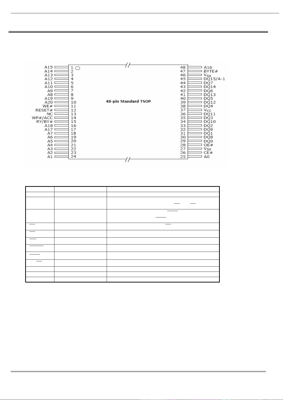
CONNECTION DIAGRAM
A15
A14
A13
A12
A11
A10
A9
A8
A19
A20
WE#
RESET#
NC
WP#/ACC
RY/BY#
A18
A17
A7
A6
A5
A4
A3
A2
A1
1
2
3
4
5
6
7
8
9
10
11
12
13
14
15
16
17
18
19
20
21
22
23
24
48-Pin Standard TSOP
ES29LV320E
48
47
46
45
44
43
42
41
40
39
38
37
36
35
34
33
32
31
30
29
28
27
26
25
A16
BYTE#
Vss
DQ15/A-1
DQ7
DQ14
DQ6
DQ13
DQ5
DQ12
DQ4
Vcc
DQ11
DQ3
DQ10
DQ2
DQ9
DQ1
DQ8
DQ0
OE#
Vss
CE#
A0
48-Ball FBGA 6 x 8 mm)
(Top View, Balls Facing Down)
C D E F G H J K
7
6
5
4
3
2
A13 A12
A9
WE#
RY/
A7
A3
A8
RESET#
WP#/
ACCBY#
A17
A4
A14
A10
NC
A18
A6
A2
A15
A16
A11 DQ7
A19
A20
A5
DQ5
DQ2
DQ0
A0A1
BYTE#
DQ14
DQ12
DQ10 DQ11 DQ3
DQ8 DQ9 DQ1
DQ15/
A-1
DQ13
Vcc
OE#CE#
Vss
DQ6
DQ4
Vss
Page 15
Y
E
95
AVR3550HD harman/kardon
ESMT
Preliminary F49L320UA/F49L320BA
32 Mbit (4M x 8/2M x 16)
3V Only CMOS Flash Memory
1. FEATURES
z Single supply v oltage 2.7V-3.6V
z Fast access time: 70/90 ns
z 4,194,304x8 / 2,097,152x16 switchable by BYTE pin
Compatible with JEDEC standard
- Pin-out, packages and software commands compatible with
single-power supply Flash
z Low po wer consumption
- 20mA typical active current
- 25uA typical standby current
z 100,000 program/erase cycles typically
z 20 Years Data Retention
z Command register architecture
- Byte Word Programming (9μs/11μs typical)
- Byte Mode : eight 8KB, sixty three 64KB sectors.
- Word Mode : eight 4K word, sixty-three 32 K word sectors.
z Auto Erase (chip & sector) and Auto Program
- Any combination of sectors can be erased concurrently;
Chip erase also provided.
- Automatically program and verify data at specified address
z Erase Suspend/Erase Resume
- Suspend or Resume erasing sectors to allow the
read/program in another sector
z Secured Silicon Sector
- 128word sector for permanent, secure identification through
an 8- word random Electronic Serial Number
- May be programmed and locked at the factory or by the
customer
- Accessible through a command sequence.
2. ORDERING INFORMATION
Part No Boot Speed Package Comments Part No Boot Speed Package Comments
F49L320UA-70TG Upper 70 ns TSOPI Pb-free F49L320UA-90TG Upper 90 ns TSOPI Pb-free
F49L320BA-70TG Bottom 70 ns TSOPI Pb-free F49L320BA-90TG Bottom 90 ns TSOPI Pb-free
3. GENERAL DESCRIPTION
The F49L320UA/F49L320BA is a 32 Megabit, 3V only CMOS
Flash memory device organized as 4M bytes of 8 bits or 2M
words of 16bits. This device is packaged in standard 48-pin
TSOP. It is designed to be programmed and erased both in
system and can in standard EPROM programmers.
With access times of 70 ns and 90 ns, the
F49L320UA/F49L320BA allows the operation of high-speed
microprocessors. The device has separate chip enable
enable
, and output enable
WE
controls. ESMT’s memory
O
CE
, write
devices reliably store memory data even after 100,000 program
and erase cycles.
The F49L320UA/F49L320BA is entirely pin and command set
compatible with the JEDEC standard for 32 Megabit Flash
memory devices. Commands are written to
The F49L320UA/F49L320BA features a sector erase architecture.
The device array is divided into eight 8KB, sixty-three 64KB for
z Ready/Busy (RY/BY )
- RY/
output pin for detection of program or erase operation
B
completion
z End of program or erase detection
- Data polling
- Toggle bits
z Hardware reset
- Hardware pin (
) resets the internal state machine to
ESETR
the read mode
z Sector Protection /Unprotection
- Hardware Protect/Unprotect any combination of sectors from
a program or erase operation.
z Low V
z Boot Sector Architecture
Write inhibit is equal to or less than 2.0V
CC
- U = Upper Boot Block
- B = Bottom Boot Block
z Packages available:
- 48-pin TSOPI
- All Pb-free products are RoHS-Compliant
z CFI (Common Flash Interface) complaint
- Provides device-specific information to the system, allowing
host software to easily reconfigure to different Flash devices.
byte mode. The device memory array is divided into eight 4K
word, sixty-three 32K word sectors for word mode. Sectors can
be erased individually or in groups without affecting the data in
other sectors. Multiple-sector erase and whole chip erase
capabilities provide the flexibility to revise the data in the
device.
The sector protect/unprotect feature disables both program and
erase operations in any combination of the sectors of the
memory. This can be achieved in-system o r via programming
equipment.
A lo w V
detector inhibits write operations on loss of power.
CC
End of program or erase is detected by the Ready/Busy status
pin, Data Polling of DQ7, or by the Toggle Bit I feature on DQ6.
Once the program or erase cycle has been successfully
completed, the device internally resets to the Read mode. The
command register using standard microprocessor write
timings.
Elite Semiconductor Memory Technology Inc. Publication Date : Jan. 2008
Revision: 0.4 1/54
Page 16
96
AVR3550HD harman/kardon
ESMT
Preliminary F49L320UA/F49L320BA
4. PIN CONFIGURATIONS
4.1 48-pin TSOP
4.2 Pin Description
Symbol Pin Name Functions
A0~A20 Address Input To provide memory addresses.
DQ0~DQ14 Data Input/Output
DQ15/A-1
CE
OE
WE
RESET
BYTE
RY/BY
VCC Power Supply To provide power
GND Ground
NC No connection
Q15 (Word mode) /
LSB addr (Byte Mode)
Chip Enable
Output Enable To gate the data output buffers.
Write Enable To control the Write operations.
Reset Hardware Reset Pin/Sector Protect Unprotect
Word/Byte selection input To select word mode or byte mode
Ready/Busy To check device operation status
To output data when Read and receive data when Write.
The outputs are in tri-state when
To bi-direction date I/O when
To input address when
To activate the device when CE is low.
BYTE
OE or CE is high.
BYTE is High
is Low
Elite Semiconductor Memory Technology Inc. Publication Date : Jan. 2008
Revision: 0.4 2/54
Page 17
97
AVR3550HD harman/kardon
ESMT
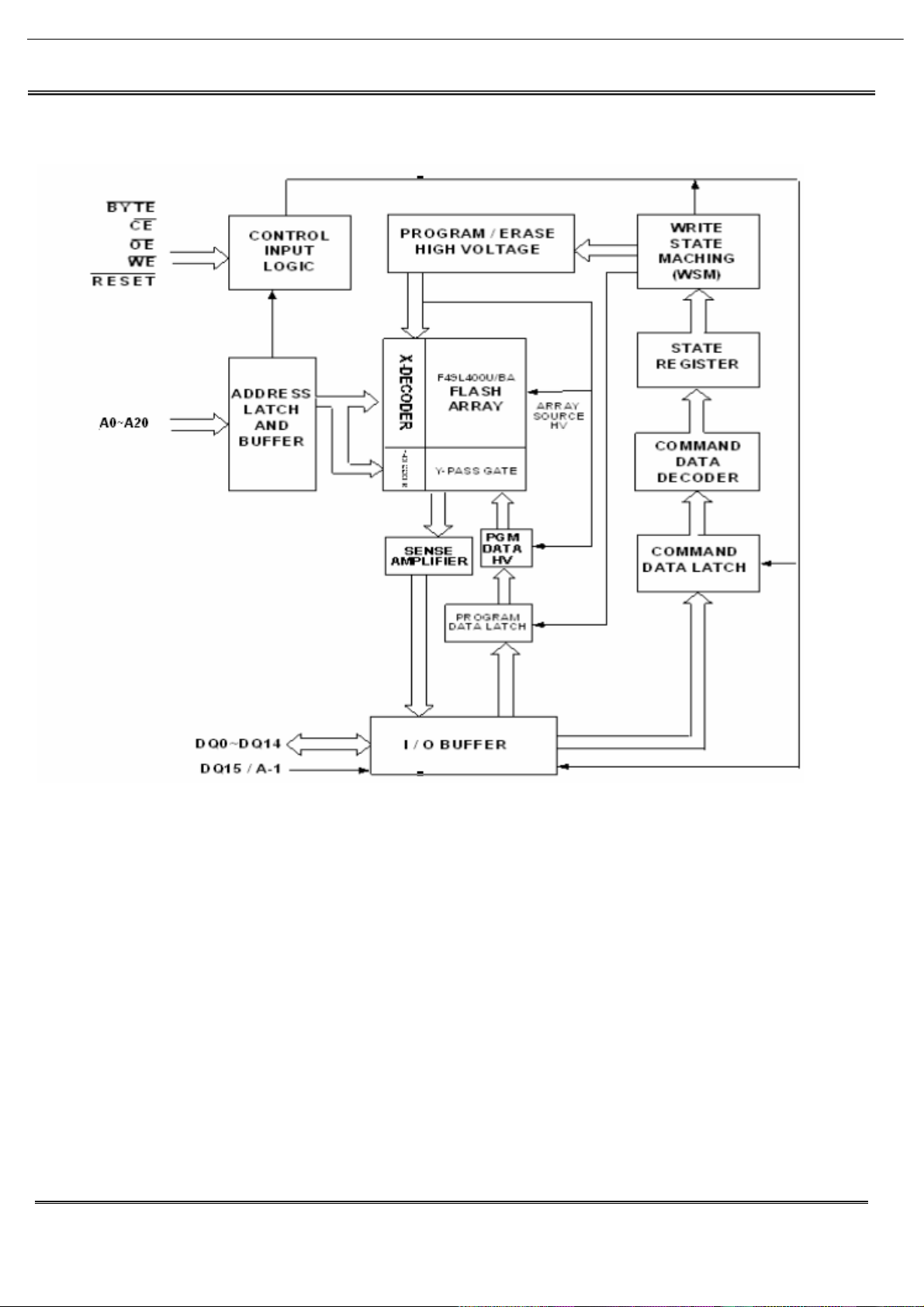
6. FUNCTIONAL BLOCK DIAGRAM
Preliminary F49L320UA/F49L320BA
Elite Semiconductor Memory Technology Inc. Publication Date : Jan. 2008
Revision: 0.4 7/54
Page 18
98
AVR3550HD harman/kardon
FLI30336
Single-chip enhanced LCD TV controller
Data Brief
Features
■ Integrated 3D video decoder
■ Flexible digital capture up to 165 MHz and
analog capture up to 162 MHz
■ VBI signal processing including WST version
2.5 support
■ Flexible DDR memory interface
■ Faroudja® TrueLife™ video enhancer
■ Advanced Picture-in-Picture (PIP) features
■ Advanced Color Management (ACM-3D) and
Adaptive Contrast Control (ACC)
■ On-chip microprocessor
■ Advanced bitmapped OSD controller
■ LCD overdrive
■ Embedded 10-bit dual-channel LVDS for
1080p and WUXGA panel support
■ Package: 416 PBGA
External Memory
CV1
CV2
CV3
YC1
YC2
YPrPb/
RGB 1
YPrPb/
RGB 2
2x24-bit or
1x30+1x16 bit
input
Analog
Front
End
Digital
Input
Port
10-bit 3D Video
Decoder and
Triple ADC
10-bit Triple
ADC
VBI Data
Proc
MUX
TTX
Decoder
Applications
■ LCD and PDP TV
■ DLP®, LCD, and LCOS front and rear
projection
10 bit
Memory
Controller
DCDi Format
Conversion
for PIP
Controller
Filters
ACM 3D
Sharpening
OSD
and ACC
Enhancer
3x3
3x3
OSD
Blend
Blend
CLUTs
Matrix
Picture
Matrix
10 bit
LVDS Tx
Output
Formatter
Dual
Channel
LVDS
TTL
RGB or
YUV
IR I/
F
Embedded
Micro
-
processor
Control Interface
LBWADC
6 channels
General
Purpose
I/O
GPIO
Audio
Delay
I2S inI2S
out
www.st.com
7
Page 19
99
AVR3550HD harman/kardon
Description FLI30336
1 Description
The FLI30336 offers high integration for advanced applications of Picture-in-Picture (PIP)
and Picture-by-Picture (PBP) with an integrated video decoder and a 3D comb filter. The
FLI30336 can power up to 1080p/WUXGA displays with the proven Faroudja DCDi Cinema
branded technology.
Special performance features such as the Faroudja DCDi Cinema video format converter,
10-bit performance in the device, and the Advanced Color Management (ACM-3D) provide
exceptional video quality. This exclusive level of video quality technology only seen on
Faroudja Home Theater Systems is now available in a single-chip solution.
The FLI30336 also comprises an integrated Analog Front-End (AFE) that includes triple
ADCs and an integrated cross-point switch. The flexible AFE ensures simple PCB design
with direct connections to TV tuners and input video connectors. In essence, the FLI30336
is the only device needed for a single LCD TV chassis supporting worldwide standards. For
regional variations, only connector and firmware changes are required.
The integrated VBI dataslicer and decoder remove the need for external components
resulting in significant cost reduction. The FLI30336 supports many worldwide VBI
standards for applications of Teletext, Closed Captioning, V-Chip, and other VBI services.
The FLI30336 can be used in digital TV solutions requiring Faroudja DCDi Cinema video
performance levels. An embedded microprocessor and a versatile OSD in a single device
will facilitate rapid development of a reliable and attractive product. The FLI30336 utilizes
the common Cortez family firmware for easy and effortless migration across different
hardware platforms within this family.
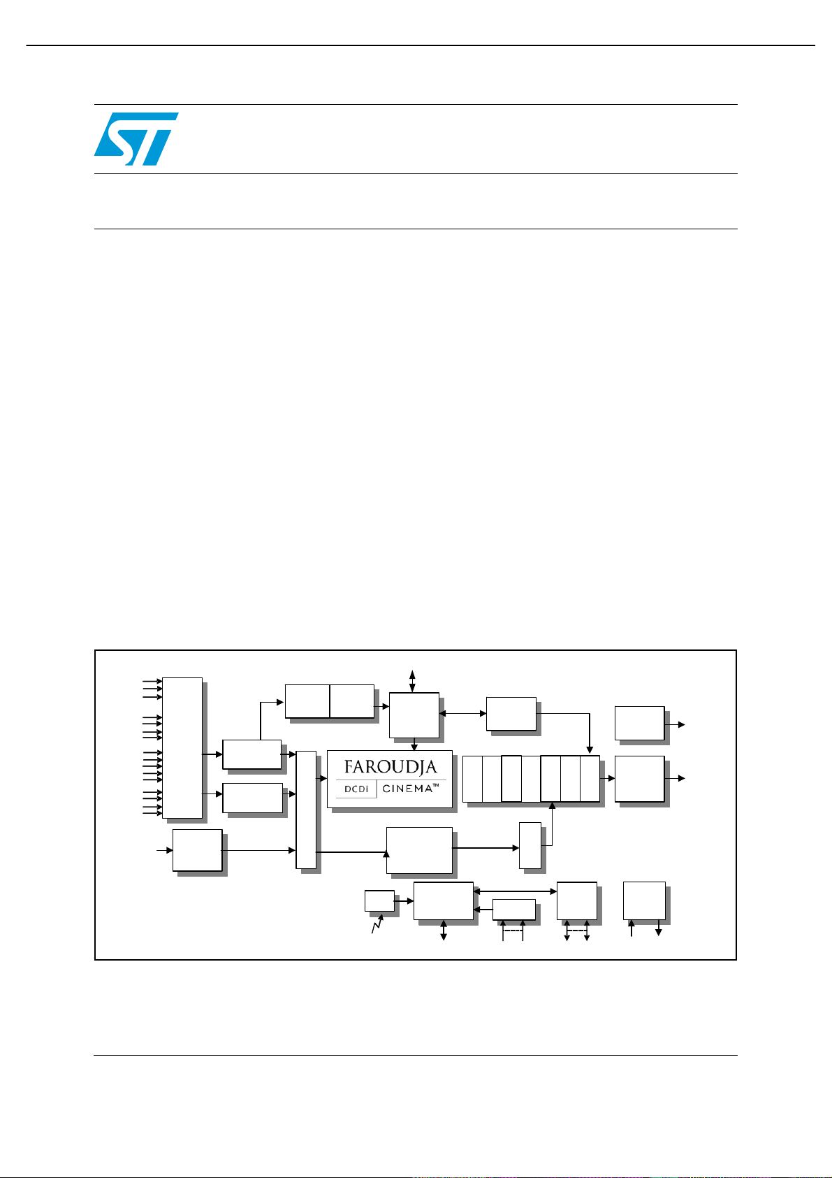
Figure 1. System diagram
DDR
SDRAM
RF
Component Video
SCART or Analog RGB
RF
TV
Tuner
16 configurable
Y/C
Optional Second
Analog Channel
MPEG-2 Decoder
analog inputs
FLI30336
Program
Flash
LVDS
Display
up to
WUXGA/
1080p
Page 20

100
AVR3550HD harman/kardon
FLI30336 Feature attributes
2 Feature attributes
● Flexible digital and analog capture
– 16 configurable analog inputs
– Direct connection from tuner or connector to analog input pin
– Supports analog RGB/YUV capture up to 162 MHz and digital input capture up to
165 MHz
– Full SCART support including RGB fast blank
– 4:4:4/4:2:2/CCIR656/601 8/16/24/30-bit digital input port
– Simple connection to JPEG and MPEG processors with a 8-bit bi-directional
media port
● Integrated 3D video decoder
– Faroudja IntelliComb™ technology
– 3D adaptive comb filters for luma–chroma separation
– Supports Composite, S-Video, and Component (including High Definition) video
input signals
– Supports all broadcast TV video standards—NTSC (North America and Japan),
PAL (I, B, G, H, M, D, N), SECAM (D, K, L, B, G)
– Supports playback video standards—NTSC443 and PAL-60
TM
– Macrovision
● VBI signal processing
– Multi-standard digital VBI dataslicer
– WST FastText page support access with > 2048 page cache
– Supports WST level 2.5
– V-chip, VPS, Closed Captioning, XDS, CGMS, and WSS decoder
– Supports VBI frame freeze
● Faroudja DCDI Cinema format conversion
– Low angle de-interlacing processing
– Per pixel Motion Adaptive De-interlacing (MADi) up to 1080i format
– Format conversion up to WUXGA resolutions
– Panoramic and anamorphic non-linear scaling
– Adaptive media display processing for 3:2 and 2:2 video content
– Special 2:2 and 3:3 film mode for improved film processing
– Adaptive 3D/TNR noise reduction
– Media noise reduction for MPEG inputs
● On-chip microprocessor
– Integrated x186-based microprocessor with rich function library
– General Purpose Inputs/Outputs (GPIOs) available for managing system devices
(keypad, backlight, NVRAM, etc.)
– Advanced power control for low power stand-by mode
– 2-wire serial master bus interface for external device control
and VCR trick mode support
3/7
Page 21

101
AVR3550HD harman/kardon
Feature attributes FLI30336
● Faroudja TrueLife video enhancer
– High performance and programmable sharpening filters with noise coring
– Programmable main channel horizontal and vertical filter coefficients
– Non-linear chroma and luma enhancement
– Removal of the DVD Chroma Upsampling Error (CUE) introduced by some
DVD sources
● Advanced Color Management (ACM-3D)
– ACM-3D allows flexible flesh-tone compensation, blue stretch, and other image
enhancements
– ACM-3D provides flexible programming, polar coordinate representation, and six-
axis color control
– ACC ensures full dynamic range is used in video content
● Picture-in-Picture (PIP)
– Programmable PIP channel horizontal and vertical filter coefficients
– Supports high performance programmable sharpening filters with noise coring
– Video PIP over full screen graphics and video backgrounds
– Supports graphics and video PIP (CVBS/S-Video/Component ED/HD) over full
screen video background (CVBS/S-Video)
– Side-by-side window support
– PIP zoom support
– DCDi Edge® processing for second channel window
● Output formats
– Dual-channel 8-bit wide TTL output
– Dual-channel 10-bit LVDS transmitters for direct connection to LCD modules
– 30-bit single-wide TTL output; 24-bit 4:2:2 YUV TTL output—12 bits per color
1080p panel support
– 120 Hz WXGA panel support using FRC and Black Frame Insertion (BFI)
technique
● Other features
– Integrated infrared decoder
– Integrated low bandwidth ADC with 6 input channels
– 4 integrated PWM outputs for LCD backlight control
– Integrated I2S audio delay to exact audio and video synchronization
– I2S channel MUX to support two I2S input streams
– Supports DDR1-500 memory devices and 512 Mb
– Reduce LCD video smearing artifacts
– Advanced bitmapped OSD controller
Page 22
MK2302S-01
MDS 2302S-01 B 1 Revision 070803
Integrated Circuit Systems, Inc. ● 5 25 Race Str eet, San Jose, CA 9512 6 ● tel (408) 295-9800 ● www.icst.com
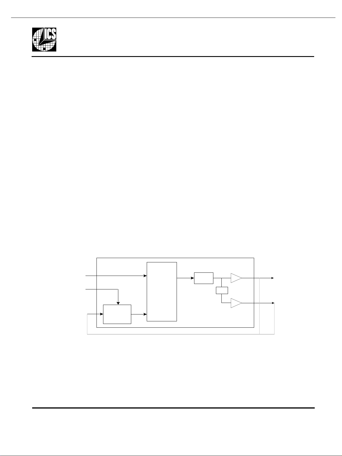
Multiplier and Zero Delay Buffer
Description
The MK2302S-01is a high performance Zero Delay
Buffer (ZDB) which integrates ICS’ proprietary
analog/digital Phase Locked Loop (PLL) techniques.
The chip is part of ICS’ ClockBlocksTM family and was
designed as a performance upgrade to meet today’s
higher speed and lower voltage requirements. The zero
delay feature means that the rising edge of the input
clock aligns with the rising edges of both output clocks,
giving the appearance of no delay through the device.
There are two outputs on the chip, one being a
low-skew divide by two of the other output.
The MK2302S-01 is ideal for synchronizing outputs in a
large variety of systems, from personal computers to
data communications to graphics/video. By allowing
off-chip feedback paths, the device can eliminate the
delay through other devices.
Features
• 8 pin SOIC package
• Low input to output skew of 250ps max
• Absolute jitter ± 500ps
• Propagation Delay ± 350ps
• Ability to choose between different multipliers from
0.5X to 16X
• Output clock frequency up to 133 MHz at 3.3V
• Can recover degraded input clock duty cycle
• Output clock duty cycle of 45/55
• Full CMOS clock swings with 25mA drive capability
at TTL levels
• Advanced, low power CMOS process
• Operating voltage of 3.3V or 5V
• Industrial temperature version available
Block Diagram
Phase
Detector,
Charge
Pump,
and Loop
Filter
divide
by N
CLK1
External feedback can come from CLK1 or CLK2 (see table on page 2)
IC L K
FBIN
S1:0
VCO
CLK2
/2
102
AVR3550HD harman/kardon
Page 23
Multiplier and Zero Delay Buffer
MK2302S-01
Pin Assignment
Clock Multiplier Decoding Table 1
(Multiplies Input clock by shown amount)
Pin Descriptions
FBIN
ICLK
GND
VDD
S0
CLK1
CLK21
2
3
4
8
7
6
5
GND
S1
1
2
3
4
8
7
6
5
8 pin (150 mil) SOIC
FBIN S1 S0 CLK1 CLK2
CLK1 0 0 2 X ICLK ICLK
CLK1 0 1 4 X ICLK 2 X ICLK
CLK1 1 0 ICLK ICLK/2
CLK1 1 1 8 X ICLK 4 X ICLK
CLK2 0 0 4 X ICLK 2 X ICLK
CLK2 0 1 8 X ICLK 4 X ICLK
CLK2 1 0 2 X ICLK ICLK
CLK2 1 1 16 X ICLK 8 XICLK
Pin
Number
Pin
Name
Pin
Type
Pin Description
1 FBIN Input Feedback clock input.
2 ICLK Input Reference clock input.
3 GND Power Connect to ground.
4 S0 Input Select 0 for output clock per decoding table above. Pull-up.
5 S1 Input Select 1 for output clock per decoding table above. Pull up.
6 CLK1 Output Clock output per table above.
7 VDD Power Connect to +3.3V or +5.0V.
8 CLK2 Output Clock output per table above. Low skew divide by two of pin 6 clock.
103
AVR3550HD harman/kardon
Page 24
Multiformat Video Encoder
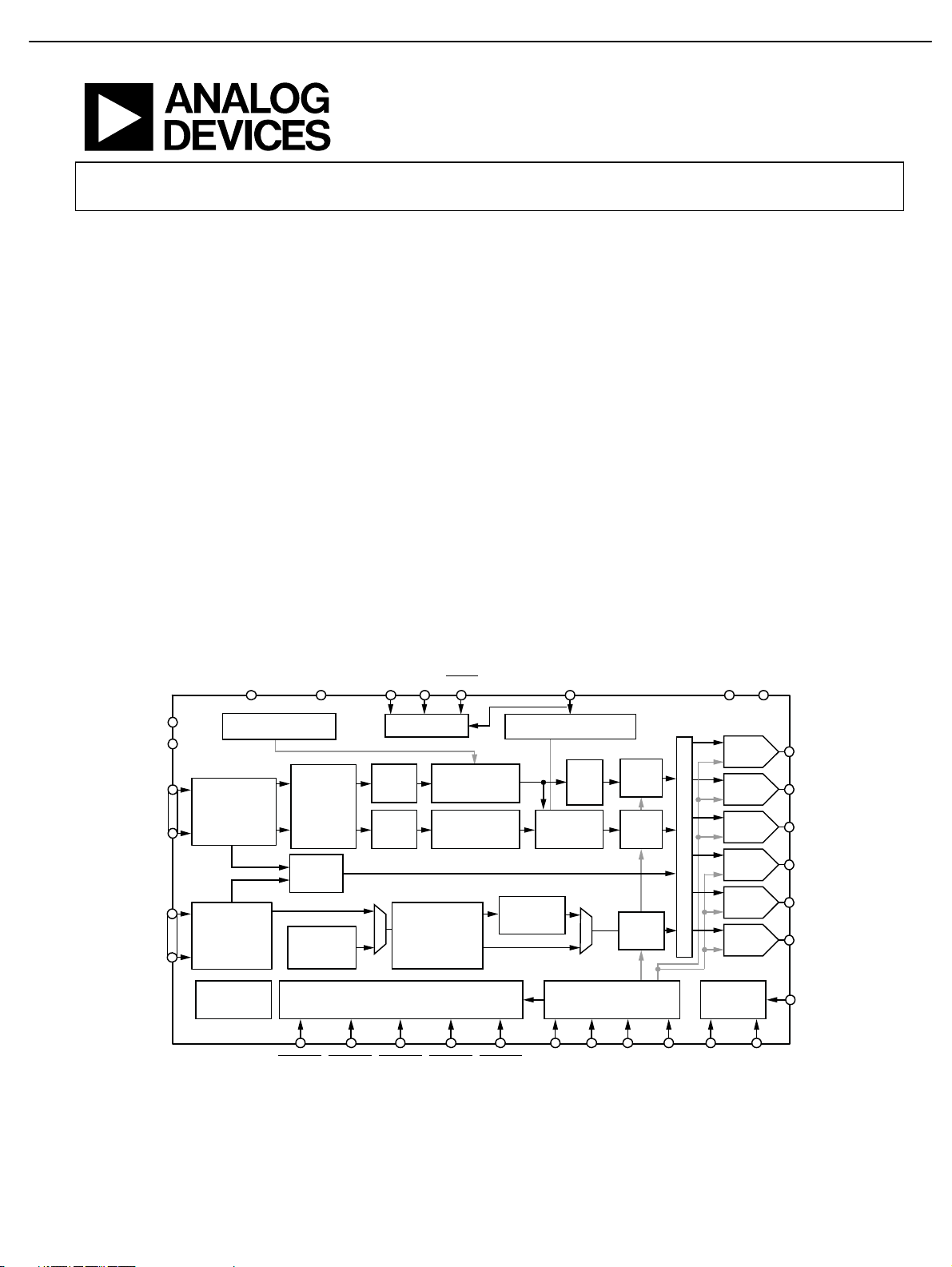
Six, 11-Bit, 297 MHz DACs
ADV7342/ADV7343
Rev. 0
Information furnished by Analog Devices is believed to be accurate and reliable. However, no
responsibility is assumed by Anal og Devices for its use, nor for any infringements of patents or ot her
rights of third parties that may result from its use. Specifications subject to change without notice. No
license is granted by implication or otherwise under any patent or patent rights of Analog Devices.
Trademarks and registered trademarks are the property of their respective owners.
One Technology Way, P.O. Box 9106, Norwood, MA 02062-9106, U.S.A.
Tel: 781.329.4700 www.analog.com
Fax: 781.461.3113 ©2006 Analog Devices, Inc. All rights reserved.
FEATURES
74.25 MHz 20-/30-bit high definition input support
Compliant with SMPTE 274M (1080i), 296M (720p),
and 240M (1035i)
6, 11-bit, 297 MHz video DACs
16× (216 MHz) DAC oversampling for SD
8× (216 MHz) DAC oversampling for ED
4× (297 MHz) DAC oversampling for HD
37 mA maximum DAC output current
NTSC M, PAL B/D/G/H/I/M/N, PAL 60 support
NTSC and PAL square pixel operation (24.54 MHz/29.5 MHz)
Multiformat video input support
4:2:2 YCrCb (SD, ED, and HD)
4:4:4 YCrCb (ED and HD)
4:4:4 RGB (SD, ED, and HD)
Multiformat video output support
Composite (CVBS) and S-Video (Y/C)
Component YPrPb (SD, ED, and HD)
Component RGB (SD, ED, and HD)
Macrovision® Rev 7.1.L1 (SD) and Rev 1.2 (ED) compliant
Simultaneous SD and ED/HD operation
EIA/CEA-861B compliance support
Programmable features
Luma and chroma filter responses
Vertical blanking interval (VBI)
Subcarrier frequency (F
SC
) and phase
Luma delay
Copy generation management system (CGMS)
Closed captioning and wide screen signaling (WSS)
Integrated subcarrier locking to external video source
Complete on-chip video timing generator
On-chip test pattern generation
On-board voltage reference (optional external input)
Serial MPU interface with dual I
2
C® and SPI® compatibility
3.3 V analog operation
1.8 V digital operation
3.3 V I/O operation
Temperature range: −40°C to +85°C
APPLICATIONS
DVD recorders and players
High definition Blu-ray DVD players
HD-DVD players
FUNCTIONAL BLOCK DIAGRAM
R
GND_IO
VDD_IO
10-BIT
SD
VIDEO
DATA
20-BIT
ED/HD
VIDEO
DATA
S_HSYNCP_HSYNC P_VSYNC P_BLANK S_VSYNC
11-BIT
DAC 1
DAC 1
11-BIT
DAC 2
DAC 2
11-BIT
DAC 3
DAC 3
11-BIT
DAC 4
DAC 4
11-BIT
DAC 5
DAC 5
11-BIT
DAC 6
DAC 6
MULTIPLEXER
REFERENCE
AND CABLE
DETECT
16x/4x OVERSAM PLING
DAC PLL
VIDEO TI MING GENERATOR
POWER
MANAGEMENT
CONTRO L
CLKIN (2) PV
DD
PGND EXT_LF (2) V
REF
COMP (2)
R
SET
(2)
ED/HD INPUT
DEINTERLEAVE
PROGRAMMABLE
HDTV FILTERS
SHARPNESS AND
ADAPTIVE FILTER
CONTROL
YCbCr
HDTV
TEST
PATTERN
GENERATOR
YCbCr
TO
RGB MATRIX
G/B
RGB
ASYNC
BYPASS
RGB
DGND (2) VDD (2)
SCL/
MOSI
SDA/
SCLK
A
LSB/
SPI_SS
SFL/
MISO
MPU PORT
SUBCARRIER FREQUENCY
LOCK (SFL )
YUV
TO
YCrCb/
RGB
PROGRAMMABLE
CHROMINANCE
FILTER
ADD
BURST
RGB/YCrCb
TO
YUV
MATRIX
4:2:2 TO 4: 4:4
HD DDR
DEINTERLEAVE
SIN/COS DDS
BLOCK
16×
FILTER
16×
FILTER
4×
FILTER
AGND
V
AA
ADD
SYNC
VBI DATA SERVICE
INSERTION
PROGRAMMABLE
LUMINANCE
FILTER
06399-001
ADV7342/ADV7343
Figure 1.
Protected by U.S. Patent Numbers 5,343,196 and 5,442,355 and other intellectual property rights.
Protected by U.S. Patent Numbers 4,631,603, 4,577,216, 4,819,098 and other intellectual property rights.
104
AVR3550HD harman/kardon
Page 25
ADV7342/ADV7343
Rev. 0 | Page 18 of 88
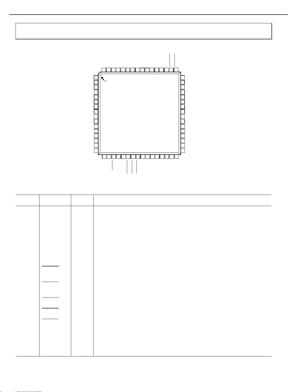
PIN CONFIGURATION AND FUNCTION DESCRIPTIONS
64
GND_IO63CLKIN_B62S761S660S559S458S357DGND56V
DD
55S254S153S052
TEST551TEST450S_HSYNC49S_VSYNC
47
R
SET1
46
V
REF
45
COMP1
42
DAC 3
43
DAC 2
44
DAC 1
48
SFL/MISO
41
V
AA
40
AGND
39
DAC 4
37
DAC 6
36
R
SET2
35
COMP2
34
PV
DD
33
EXT_LF1
38
DAC 5
2
TEST0
3
TEST1
4
Y0
7
Y3
6
Y2
5
Y1
1
V
DD_IO
8
Y4
9
Y5
10
V
DD
12
Y6
13
Y7
14
TEST2
15
TEST3
16
C0
11
DGND
17C118C219
ALSB/SPI_SS
20
SDA/SCLK
21
SCL/MOSI
22 23
P_HSYNC
24
P_VSYNC
25
P_BLANK
26
C4
C327C528C629C7
30
CLKIN_A
31 32
PGND
PIN 1
ADV7342/ADV7343
TOP VIEW
(Not to Scale)
EXT_LF2
06399-021
Figure 21. Pin Configuration
Table 13. Pin Function Descriptions
Pin No. Mnemonic
Input/
Output
Description
13, 12,
9 to 4
Y7 to Y0 I 8-Bit Pixel Port. Y0 is the LSB. Refer to Table 31 for input modes.
29 to 25,
18 to 16
C7 to C0 I 8-Bit Pixel Port. C0 is the LSB. Refer to Table 31 for input modes.
62 to 58,
55 to 53
S7 to S0 I 8-Bit Pixel Port. S0 is the LSB. Refer to Table 31 for input modes.
52, 51, 15,
14, 3, 2
TEST5 to
TEST0
I Unused. These pins should be connected to DGND.
30 CLKIN_A I Pixel Clock Input for HD Only (74.25 MHz), ED1 Only (27 MHz or 54 MHz) or SD Only (27 MHz).
63 CLKIN_B I
Pixel Clock Input for Dual Modes Only. Requires a 27 MHz reference clock for ED operation or a
74.25 MHz reference clock for HD operation.
50
S_HSYNC
I/O
SD Horizontal Synchronization Signal. This pin can also be configured to output an SD, ED, or HD
horizontal synchronization signal. See the External Horizontal and Vertical Synchronization
Control section.
49
S_VSYNC
I/O
SD Vertical Synchronization Signal. This pin can also be configured to output an SD, ED, or HD
vertical synchronization signal. See the External Horizontal and Vertical Synchronization Control
section.
22
P_HSYNC
I
ED/HD Horizontal Synchronization Signal. See the External Horizontal and Vertical
Synchronization Control section.
23
P_VSYNC
I
ED/HD Vertical Synchronization Signal. See the External Horizontal and Vertical Synchronization
Control section.
24
P_BLANK
I ED/HD Blanking Signal. See the External Horizontal and Vertical Synchronization Control section.
48 SFL/MISO I/O
Multifunctional Pin: Subcarrier Frequency Lock (SFL) Input/SPI Data Output. The SFL input is
used to drive the color subcarrier DDS system, timing reset, or subcarrier reset.
47 R
SET1
I
This pin is used to control the amplitudes of the DAC 1, DAC 2, and DAC 3 outputs. For full-drive
operation (for example, into a 37.5 Ω load), a 510 Ω resistor must be connected from R
SET1
to
AGND. For low drive operation (for example, into a 300 Ω load), a 4.12 kΩ resistor must be
connected from R
SET1
to AGND.
105
AVR3550HD harman/kardon
Page 26

ADV7342/ADV7343
Rev. 0 | Page 19 of 88
Pin No. Mnemonic
Input/
Output Description
36 R
SET2
I
This pin is used to control the amplitudes of the DAC 4, DAC 5, and DAC 6 outputs. A 4.12 kΩ
resistor must be connected from R
SET2
to AGND.
45, 35
COMP1,
COMP2
O Compensation Pins. Connect a 2.2 nF capacitor from both COMP pins to V
AA
.
44, 43, 42
DAC 1, DAC 2,
DAC 3
O DAC Outputs. Full and low drive capable DACs.
39, 38, 37
DAC 4, DAC 5,
DAC 6
O DAC Outputs. Low drive only capable DACs.
21 SCL/MOSI I Multifunctional Pin: I2C Clock Input/SPI Data Input.
20 SDA/SCLK I/O Multifunctional Pin: I2C Data Input/Output. Also, SPI clock input.
19
ALSB/SPI_SS
I Multifunctional Pin: This signal sets up the LSB
2
of the MPU I2C address. Also, SPI slave select.
46 V
REF
Optional External Voltage Reference Input for DACs or Voltage Reference Output.
41 VAA P Analog Power Supply (3.3 V).
10, 56 VDD P
Digital Power Supply (1.8 V). For dual-supply configurations, V
DD
can be connected to other 1.8 V
supplies through a ferrite bead or suitable filtering.
1 V
DD_IO
P Input/Output Digital Power Supply (3.3 V).
34 PVDD P
PLL Power Supply (1.8 V). For dual-supply configurations, PV
DD
can be connected to other 1.8 V
supplies through a ferrite bead or suitable filtering.
33 EXT_LF1 I External Loop Filter for On-Chip PLL 1.
31 EXT_LF2 I External Loop Filter for On-Chip PLL 2.
32 PGND G PLL Ground Pin.
40 AGND G Analog Ground Pin.
11, 57 DGND G Digital Ground Pin.
64 GND_IO G Input/Output Supply Ground Pin.
1
ED = enhanced definition = 525p and 625p.
2
LSB = least significant bit. In the ADV7342, setting the LSB to 0 sets the I2C address to 0xD4. Setting it to 1 sets the I2C address to 0xD6. In the ADV7343, setting the
LSB to 0 sets the I2C address to 0x54. Setting it to 1 sets the I2C address to 0x56.
106
AVR3550HD harman/kardon
Page 27
107
AVR3550HD harman/kardon
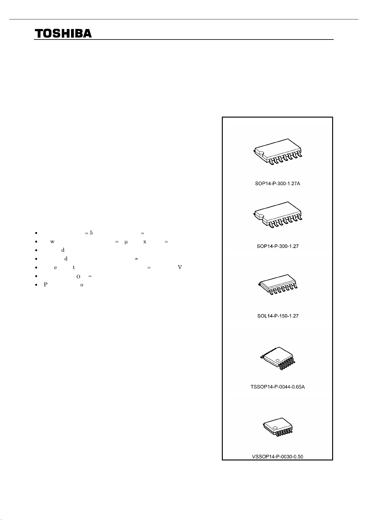
TC74VHC14F/FN/FT/FK
TOSHIBA CMOS Digital Integrated Circuit Silicon Monolithic
TC74VHC14F,TC74VHC14FN,TC74VHC14FT,TC74VHC14FK
Hex Schmitt Inverter
The TC74VHC14 is an advanced high speed CMOS SCHMITT
INVERTER fabricated with silicon gate C
2
MOS technology.
It achieves the high speed operation similar to equivalent
Bipolar Schottky TTL while maintaining the CMOS low power
dissipation.
Pin configuration and function are the same as the
TC74VHC04 but the inputs have hysteresis and with its schmitt
trigger function, the TC74VHC14 can be used as a line receivers
which will receive slow input signals.
An input protection circuit ensures that 0 to 5.5 V can be
applied to the input pins without regard to the supply voltage.
This device can be used to interface 5 V to 3 V systems and two
supply systems such as battery back up. This circuit prevents
device destruction due to mismatched supply and input voltages.
Features
High speed: tpd 5.5 ns (typ.) at VCC 5 V
Low power dissipation: I
Power down protection is provided on all inputs.
Balanced propagation delays: t
Wide operating voltage range: V
Low noise: V
Pin and function compatible with 74ALS14
OLP
0.8 V (max)
2 A (max) at Ta 25°C
CC
t
CC (opr)
pHL
2 V to 5.5 V
pLH
Weight
SOP14-P-300-1.27A : 0.18 g (typ.)
SOP14-P-300-1.27 : 0.18 g (typ.)
SOL14-P-150-1.27 : 0.12 g (typ.)
TSSOP14-P-0044-0.65A : 0.06 g (typ.)
VSSOP14-P-0030-0.50 : 0.02 g (typ.)
Note: xxxFN (JEDEC SOP) is not available in
Japan.
TC74VHC14F
TC74VHC14FN
TC74VHC14FT
TC74VHC14FK
Page 28
108
AVR3550HD harman/kardon
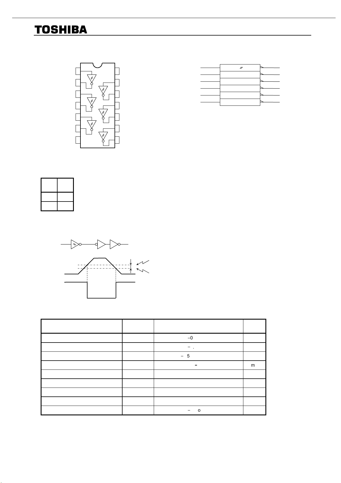
TC74VHC14F/FN/FT/FK
Pin Assignment IEC Logic Symbol
1A
1Y
2A
2Y
(1)
VCC
1
2
3
4
14
13
12
11
6A
6Y
5A
1A
2A
3A
4A
5A
6A
(3)
(5)
(9)
(11)
(13)
(2)
(4)
(6)
(8)
(10)
(12)
1Y
2Y
3Y
4Y
5Y
6Y
3A
3Y
GND
5
6
7
10
9
8
(top view)
Truth Table
A Y
L H
H L
System Diagram, Waveform
A
(A)
V
IN
5Y
4A
4Y
Y
V
H
V
P
V
N
V
(Y)
OUT
Absolute Maximum Ratings (Note)
Characteristics Symbol Rating Unit
Supply voltage range VCC
DC input voltage VIN
DC output voltage V
OUT
Input diode current IIK
Output diode current IOK ±20 mA
DC output current I
±25 mA
OUT
DC VCC/ground current ICC ±50 mA
Power dissipation PD 180 mW
Storage temperature T
stg
Note: Exceeding any of the absolute maximum ratings, even briefly, lead to deterioration in IC performance or
even destruction.
0.5 to 7.0 V
0.5 to 7.0 V
0.5 to VCC + 0.5 V
20 mA
65 to 150 °C
Page 29

109
AVR3550HD harman/kardon
SIL 9185
Page 30

110
AVR3550HD harman/kardon
Page 31

111
AVR3550HD harman/kardon
Page 32

112
AVR3550HD harman/kardon
Page 33

113
AVR3550HD harman/kardon
Page 34

114
AVR3550HD harman/kardon
Page 35

115
AVR3550HD harman/kardon
Page 36

116
AVR3550HD harman/kardon
Page 37

117
AVR3550HD harman/kardon
Page 38

118
AVR3550HD harman/kardon
Page 39

119
AVR3550HD harman/kardon
Page 40

120
AVR3550HD harman/kardon
Page 41

121
AVR3550HD harman/kardon
Page 42

122
AVR3550HD harman/kardon
Page 43

123
AVR3550HD harman/kardon
Page 44

124
AVR3550HD harman/kardon
Page 45

125
AVR3550HD harman/kardon
Page 46

126
AVR3550HD harman/kardon
Page 47

127
AVR3550HD harman/kardon
Page 48

128
AVR3550HD harman/kardon
Page 49

129
AVR3550HD harman/kardon
Page 50

130
AVR3550HD harman/kardon
ESMT
F25L004A
4Mbit (512Kx8)
3V Only Serial Flash Memory
FEATURES
y Single supply voltage 2.7~3.6V
y Speed
- Read max frequency : 33MHz
- Fast Read max frequency : 50MHz; 75MHz; 100MHz
y Low power consumption
- typical active current
- 15
μ A typical standby current
y Reliability
- 100,000 typical program/erase cycles
- 20 years Data Retention
y Program
- Byte program time 7
y Erase
- Chip erase time 4s(typical)
- Sector erase time 60ms(typical),
block erase time 1sec (typical)
μ s(typical)
ORDERING INFORMATION
y Auto Address Increment (AAI) WORD Programming
- Decrease total chip programming time over
Byte-Program operations
y SPI Serial Interface
- SPI Compatible : Mode 0 and Mode3
y End of program or erase detection
y Write Protect (WP)
y Hold Pin (
y Package available
- 8-pin SOIC 150-mil
- 8-pin SOIC 200-mil
HOLD)
Part No. Speed Package COMMENTS
F25L004A -50PG 50MHz
F25L004A -100PG 100M Hz
F25L004A -50PAG 50MHz
8 lead
SOIC
8 lead
SOIC
8 lead
SOIC
150 mil
150 mil
200 mil
Pb-free
Pb-free
Pb-free
GENERAL DESCRIPTION
The F25L004A is a 4Megablt, 3V only CMOS Serial Flash
memory device organized as 512K bytes of 8 bits. This device is
packaged in 8-lead SOIC 200mil. ESMT’s memory devices
reliably store memory data even after 100,000 program and
erase cycles.
The F25L004A features a sector erase architecture. The device
memory array is divided into 128 uniform sectors with 4K byte
each ; 8 uniform blocks with 64K byte each. Sectors can be
Part No. Speed Package COMMENTS
F25L004A –100PAG 100MHz
F25L004A –50DG 50MHz
F25L004A –100DG 100MHz
erased individually without affecting the data in other sectors.
Blocks can be erased individually without affecting the data in
other blocks. Whole chip erase capabilities provide the flexibility
to revise the data in the device.
The sector protect/unprotect feature disables both program and
erase operations in any combination of the sectors of the
memory.
8 lead
SOIC
8 lead
PDIP
8 lead
PDIP
200 mil
300 mil
300 mil
Pb-free
Pb-free
Pb-free
Elite Semiconductor Memory Technology Inc.
Revision: 1.2 1/32
Publication Date: Apr. 2007
Page 51

131
AVR3550HD harman/kardon
ESMT
PIN CONFIGURATIONS
8-PIN SOIC
F25L004A
0
CE
SO
WP
VSS
1 8
2 7
3 6
4 5
VDD
HOLD
SCK
SI
8-PIN PDIP
CE
SO
WP
VSS
1 8
2 7
3 6
4 5
VDD
HOLD
SCK
SI
Elite Semiconductor Memory Technology Inc.
Revision: 1.2 2/32
Publication Date: Apr. 2007
Page 52

132
AVR3550HD harman/kardon
ESMT
F25L004A
PIN Description
Symbol Pin Name Functions
SCK Serial Clock
SI Serial Data Input
SO Serial Data Output
CE
WP
HOLD
VDD Power Supply To provide power.
VSS Ground
Chip Enable
Write Protect
Hold
To provide the timing for serial input and
output operations
To transfer commands, addresses or data
serially into the device.
Data is latched on the rising edge of SCK.
To transfer data serially out of the device.
Data is shifted out on the falling edge of
SCK.
To activate the device when CE is low.
The Write Protect (
enable/disable BPL bit in the status
register.
To temporality stop serial communication
with SPI flash memory without resetting
the device.
WP ) pin is used to
FUNTIONAL BLOCK DIAGRAM
Address
Buffers
and
Latches
X-Decoder
Control Logic
Flash
Y-Decoder
I/O Butters
and
Data Latches
Serial Interface
CE
SCK
SI
WPSO HOLD
Page 53

133
AVR3550HD harman/kardon
Page 54

134
AVR3550HD harman/kardon
Page 55

Copyright 2008 Cirrus Logic SEP ‘08
DS752PP7
32-bit High Definition Audio Decoder DSP
Family with Dual DSP Engine Technology
CS4970x4 Data Sheet
http://www.cirrus.com
FEATURES
Multi-standard 32-bit High Definition Audio Decoding plus
Post Processing
Supports high-definition audio formats including:
— Dolby Digital® Plus
—Dolby® TrueHD
—DTS-HD™ High Resolution Audio
—DTS-HD™ Master Audio
—DSD
®
Additional Applications Library
— Dolby Digital® EX, Dolby® Pro Logic® IIx, Dolby
Headphone
®
, Dolby® Virtual Speaker
®
—DTS-ES 96/24™, DTS-ES™ Discrete 6.1, D T S-ES™
Matrix 6.1
— AAC
™
Multichannel 5.1
—SRS® CS2® and TSXT
®
—THX® Ultra2™, THX® ReEQ
™
— Crossbar Mixer, Sign al Gen e rat o r
— Advanced Post-Processor including: 7.1 Bass Manager,
Tone Control, 11- Band Parametric EQ, Delay, 1:2
Upsampler
— Microsoft® HDCD
®
— Th omson MP3 Surround, DTS:Neo6™, DSD-to-PCM
Conversion, Neural Surround, Cirrus Original MultiChannel Surround 2 (COMS2), and more. Please contact
your local FAE for more information on available
applications.
Up to 12 Channels of 32-bit Serial A udio Input
Customer Software Security Keys
6 Channel DSD® Input
16 Ch x 32-bit PCM Out with Du al 19 2kHz SPDIF Tx
Two SPI™/I2C®, One Parallel and One UART Port
Large On-chip X, Y, and Program RAM & ROM
SDRAM and Serial Flash Memory Support
The CS4970x4 DSP family is an enhanced version of the
CS4953x DSP family with higher overall performance. In
addition to all the mainstream audio processing codes in onchip ROM that the CS4953x DSP offers, the CS4970x4 device
family also supports the decoding of major high-definition
audio formats. Additionall y, the CS4970x4, a dual -c ore d evi ce,
performs the high-definition audio decoding on the first core,
leaving the second core available for audio post-pro cessing and
audio enhancement. The CS4970x4 device will support the
most deman ding au dio pos t pro cessing requi remen ts. It i s also
designed as an easy upgrade path to systems currently using
the CS495xx or CS4953x device with minor hardware and
software changes.
Ordering Information
See
page 30 for ordering information.
32-bit
DSP A
D
M
A
32-bit
DSP B
Ext. Memory Controller
P
S/PDIF
X Y P X Y
Serial
Control 1
16 Ch PCM
Audio Out
Serial
Control 2
Parallel
Control
GPIOUART Debug
STC
TMR1
TMR2
PLL
S/PDIF
12 Ch. Audio In /
6 Ch. SACD In
Preliminary Product Information
This document contains information for a new product.
Cirrus Logic reserves the right to modify this product without notice.
135
AVR3550HD harman/kardon
Page 56

CS4970x4 Data Sheet
32-bit High Definition Audio Decoder DSP Family
8. Device Pin-Out Diagram
8.1 128-Pin LQFP Pin-Out Diagram
Figure 20. 128-Pin LQFP Pin-Out Diagram
GPIO2, UART_TXD
GPIO1, UART_RXD
GPIO0, UART_CLK, EE_CS#
XTO
VDD7
GND7
VDDIO7
XTI
GNDIO7
GNDA
PLL_REF_RES
VDDA (3.3V)
VDD8
GND8
GPIO13, DAI1_DATA2, TM2, DSD2
GPIO14, DAI1_DATA3, TM3, DSD3
DAI1_DATA0, TM0, DSD0
GPIO12, DAI1_DATA1, TM1, DSD1
GPIO6, PCP_CS#, SCP2_CS#
GPIO38, PCP_WR# / DS#, SCP2_CLK
VDD6
GND6
GPIO10, PCP_A2 / A10, SCP2_MOSI
GPIO8, PCP_IRQ#, SCP2_IRQ#
GPIO37, SCP1_BSY#, PCP_BSY
#
VDDIO6
GPIO11, PCP_A3, AS#, SCP2_MISO / SDA
GNDIO6
GPOI9, SCP1_IRQ#
GPIO34, SCP1__MISO / SDA
GPIO33, SCP1_MOSI
GPIO35, SCP1_CLK
VDD5
VDDIO5
GND5
GNDIO5
SD_CAS#
SD_RAS#
SD_A3, EXT_A3
SD_A2, EXT_A2
SD_A1, EXT_A1
SD_A0, EXT_A0
SD_A10, EXT_A10
SD_A11, EXT_A1
1
VDD4
GND4
SD_CS#
SD_A4, EXT_A4
SD_A5, EXT_A5
SD_A6, EXT_A6
SD_A7, EXT_A7
SD_A8, EXT_A8
SD_CLKEN
SD_A9, EXT_A9
VDDIO4
GNDIO4
SD_CLKOUT
SD_CLKIN
SD_D10, EXT_D1
0
SD_D11, EXT_D1
1
SD_D12, EXT_D1
2
VDD3
GND3
SD_D13, EXT_D1
3
SD_D14, EXT_D1
4
SD_D15, EXT_D1
5
SD_DQM1
SD_D7, EXT_D7
SD_D6, EXT_D6
VDDIO3
GNDIO3
SD_D5, EXT_D5
SD_DQM0
SD_D4, EXT_D4
SD_D3, EXT_D3
SD_D2, EXT_D2
G
PIO17, DAO1_DATA3 / XMTA
GPIO15, DAO1_DATA1, HS1
DAO1_DATA0, HS 0
DAO1_LRCLK
DAI1_LRCLK, DSD4
DAO_MCLK
GPIO20, DAO2_DATA2
DAI1_SCLK, DSD-CLK
VDD1
GND1
DAO1_SCLK
GPIO16, DAO1_DATA2, HS2
GPIO23,
DAO2_LRCLK
RESET#
VDDIO1
GPIO22, DAO2_SCLK
GNDIO1
GPIO18, DAO2_D ATA0, HS3
GPIO19, DAO2_D ATA1, HS4
VDD2
GND2
GPIO26, DAO2_ DATA3 / XMTB/UART_TX_ E N
VDDIO2
GNDIO2
SD_WE#
SD_D0, EXT_D0
SD_D1, EXT_D1
SD_D8, EXT_D8
SD_D9, EXT_D9
SD_A12, EXT_A1
2
SD_BA1, EXT_A14
SD_BA0, EXT_A13
GPIO7, SCP1_CS#, IOWAIT
VDDIO8
GNDIO8
EXT_A15
EXT_A16
EXT_A17
EXT_A18
EXT_A19
EXT_CS1#
EXT_OE#
EXT_WE#
GPIO3, DDAC
TEST
DBDA
DBCK
XTAL_OUT
GPIO43, BDI_CLK, DAI2_SCLK
G
PIO42, BDI_REQ# , DAI2_LRCLK, PCP_IRQ# / BSY#
BDI_DATA, DAI2_DATA, DSD5
EXT_CS2#
10
15
20
25
30
5
35
1
125
120
115
110
105
95
90
85
80
75
70
65
100
40
45
50
55
60
CS497xx4
128-Pin LQFP
136
AVR3550HD harman/kardon
Page 57

CS4970x4 Data Sheet
32-bit High Definition Audio Decoder DSP Family
8.2 144-Pin LQFP Pin-Out Diagram
Figure 21. 144-Pin LQFP Pin-Out Diagram
GPIO11, PCP_A3, AS#, SCP2_MISO / SDA
SD_A11, EXT_A11
GPIO26
G
PIO21, DAO2_DATA3 / XMTB, UART_TX_ENABLE
SD_A12, EXT_A12
G
PIO42, BDI_REQ# , DAI2_LRCLK, PCP_IRQ# / BSY#
113
116
119
122
126
129
130
133
136
139
109
110
115
120
125
135
140
144
CS497xx4
144-Pin LQFP
GPIO25, UART_TXD, EE_CS#
GPIO24, UART_RXD
GPIO31, UART_CLK
SD_D7, EXT_D7
SD_D6, EXT_D6
SD_D5, EXT_D5
SD_DQM0
SD_D4, EXT_D4
SD_D3, EXT_D3
SD_D2, EXT_D2
GPIO17, DAO1_DATA3 / XMTA
GPIO15, DAO1_DATA1, HS1
DAO1_DATA0, HS0
DAO1_LRCLK
DAO_MCLK
GPIO20, DAO2_DATA2
VDD1
GND1
DAO1_SCLK
GPIO16, DAO1_DATA2, HS2
GPIO23, DAO2_LRCLK
VDDIO1
GPIO22, DAO2_SCLK
GNDIO1
GPIO18, DAO2_DATA0, HS3
GPIO19, DAO2_DATA1, HS4
VDD2
GND2
VDDIO2
GNDIO2
GPIO28, DDAC
GPIO29, XMTA_IN
TEST
DBDA
DBCK
1
5
9
10
13
18
21
24
27
33
36
15
25
30
35
SD_A3, EXT_A3
SD_A2, EXT_A2
SD_A1, EXT_A1
SD_A0, EXT_A0
VDD4
GND4
SD_A4, EXT_A4
SD_A5, EXT_A5
SD_A6, EXT_A6
SD_A7, EXT_A7
SD_A8, EXT_A8
SD_CLKEN
SD_A9, EXT_A9
VDDIO4
GNDIO4
SD_CLKOUT
SD_CLKIN
SD_D10, EXT_D1
0
SD_D11, EXT_D1
1
SD_D12, EXT_D1
2
VDD3
GND3
SD_D13, EXT_D1
3
SD_D14, EXT_D1
4
SD_D15, EXT_D1
5
SD_DQM1
VDDIO3
GNDIO3
SD_D0, EXT_D0
SD_D1, EXT_D1
SD_D8, EXT_D8
SD_D9, EXT_D9
EXT_CS2#
EXT_WE#
69
66
63
60
57
54
47
44
37
40
45
50
55
65
70
72
GPIO39, PCP_CS#, SCP2_CS#
GPIO38, PCP_WR# / DS#, SCP2_CLK
VDD6
GPIO40, PCP_RD# / RW#
GND6
GPIO10, PCP_A2 / A10, SCP2_MOSI
GPIO41, PCP_IRQ#, SCP2_IRQ#
GPIO37, SCP1_BSY#, PCP_BSY#
VDDIO6
GNDIO6
GPOI36, SCP1_IRQ#
GPIO34, SCP1__MISO / SDA
GPIO33, SCP1_M OSI
GPIO35, SCP1_CLK
VDD5
VDDIO5
GND5
GNDIO5
SD_CAS#
SD_RAS#
SD_A10, EXT_A10
SD_CS#
RESET#
SD_WE#
SD_BA1, EXT_A14
SD_BA0, EXT_A13
GPIO32, SCP1_CS#, IOWAIT
EXT_A15
EXT_A16
EXT_A17
EXT_A18
EXT_A19
EXT_CS1#
EXT_OE#
GPIO30, XMTB_IN
101
98
94
91
86
83
767375
80
85
90
95
100
105
108
GPIO1, PCP_AD1 / D1
GPIO0, PCP_AD0 / D0
XTO
VDD7
GND7
VDDIO7
XTI
GNDIO7
GNDA
NC
PLL_REF_RES
VDDA (3.3V)
VDD8
GND8
GPIO13, DAI1_DATA2, TM2, DSD2
GPIO14, DAI1_DATA3, TM3, DSD3
DAI1_DATA0, TM0, DSD0
GPIO12, DAI1_DATA1, TM1, DSD1
GPIO2, PCP_AD2 / D2
GPIO3, PCP_AD3 / D3
GPIO4, PCP_AD4 / D4
GPIO5, PCP_AD5 / D5
GPIO6, PCP_AD6 / D6
GPIO7, PCP_AD7 / D7
GPIO9, PCP_A1 / A9
DAI1_LRCLK, DSD4
DAI1_SCLK, DSD-CLK
VDDIO8
GNDIO8
GPIO8, PCP_A0 / A8
GPIO27
XTAL_OUT
GPIO43, BDI_CLK, DAI2_SCLK
BDI_DATA, DAI2_DATA, DSD5
137
AVR3550HD harman/kardon
Page 58

138
AVR3550HD harman/kardon
ESMT M12L16161A
SDRAM 512K x 16Bit x 2Banks
Synchronous DRAM
FEATURES
z JEDEC standard 3.3V power supply
z LVTTL compatible with multiplexed address
z Dual banks operation
z MRS cycle with address key programs
- CAS Latency (2 & 3 )
- Burst Length (1, 2, 4, 8 & full page)
- Burst Type (Sequential & Interleave)
z All inputs are sampled at the positive going edge of the
system clock
z Burst Read Single-bit Write operation
z DQM for masking
z Auto & self refresh
z 32ms refresh period (2K cycle)
GENERAL DESCRIPTION
The M12L16161A is 16,777,216 bits synchronous high
data rate Dynamic RAM organized as 2 x 524,288 words by
16 bits, fabricated with high performance CMOS technology.
Synchronous design allows precise cycle control with the
use of system clock I/O transactions are possible on every
clock cycle. Range of operating frequencies, programmable
burst length and programmable latencies allow the same
device to be useful for a variety of high bandwidth, high
performance memory system applications.
ORDERING INFORMATION
Part NO. MAX Freq. PACKAGE COMMENTS
M12L16161A-5TG
M12L16161A-7TG
M12L16161A-7BG
200MHz
143MHz
143MHz
TSOP(II) Pb-free
TSOP(II) Pb-free
VFBGA Pb-free
PIN CONFIGURATION (TOP VIEW)
VDD
DQ0
DQ1
V
SSQ
DQ2
DQ3
V
DDQ
DQ4
DQ5
V
SSQ
DQ6
DQ7
V
DDQ
LDQM
WE
CAS
RAS
CS
BA
A10/AP
A0
A1
A2
A3
V
DD
1
2
3
4
5
6
7
8
9
10
11
12
13
14
15
16
17
18
19
20
21
22
23
24
25
V
SS
50
DQ15
49
DQ14
48
V
SSQ
47
DQ13
46
DQ12
45
V
DDQ
44
DQ11
43
DQ10
42
V
SSQ
41
DQ9
40
DQ8
39
V
DDQ
38
N.C/RFU
37
UDQM
36
CLK
35
CKE
34
N.C
33
A9
32
A8
31
A7
30
A6
29
A5
28
A4
27
V
SS
26
50PIN TSOP(II)
(400mil x 825mil)
(0.8 mm PIN PITCH)
1234567
DQ15
VSS
A
B
DQ14 VSSQ
DQ13 VDDQ
C
D
DQ12 DQ11
E
DQ10 VSSQ
F
DQ9
VDDQ
G
DQ8
NC
H
NC
NC
NC UDQM
J
NC CLK
K
CKE
A11
A8 A7
A6 A5
VSS A4
NC
A9
L
M
N
P
R
DQ0
VDD
VDDQ DQ1
VSSQ
DQ2
DQ4 DQ3
VDDQ
DQ5
VSSQ
DQ6
NC DQ7
NC
LDQM WE
RAS
CAS
NC
NC NC
A0 A10
A2
A3 VDD
NC
CS
A1
60 BallVFBGA
(6.4x10.1mm)
(0.65mm ball pitch)
Elite Semiconductor Memory Technology Inc. Publication Date : May. 2005
Page 59

139
AVR3550HD harman/kardon
ESMT M12L16161A
FUNCTIONAL BLOCK DIAGRAM
I/O Control
Bank Select
Row Buffer
Refresh Counter
Address Register
CLK
ADD
LCKE
LRAS LCBR
CLK
CKE
LCBR
LRAS
CS
Row Decoder
Col. Buffer
LWE
Timing Regi ster
RAS CAS WE
Data Input Regi ster
512K x 16
512K x 16
Column Decoder
Latency & Burst Length
Programming Regist er
LCAS
LWCBR
L(U)DQM
Sense AMP
Output Buffer
LDQM
LWE
LDQM
DQi
PIN FUNCTION DESCRIPTION
Pin Name Input Function
CLK
CS
CKE
A0 ~ A10/AP
BA
RAS
CAS
WE
L(U)DQM
System Clock
Chip Select
Clock Enable
Address
Bank Select Address
Row Address Strobe
Column Address Strobe
Write Enable
Data Input / Output Mask
Active on the positive going edge to sample all inputs.
Disables or enables device operation by masking or enabling all inputs except
CLK, CKE and L(U)DQM.
Masks system clock to freeze operation from the next clock cycle.
CKE should be enabled at least one cycle prior to new command.
Disable input buffers for power down in standby.
Row / column addresses are multiplexed on the same pins.
Row address : RA0 ~ RA10, column address : CA0 ~ CA7
Selects bank to be activated during row address latch time.
Selects bank for read/write during column address latch time.
Latches row addresses on the positive going edge of the CLK with
Enables row access & precharge.
Latches column addresses on the positive going edge of the CLK with
CASlow.
Enables column access.
Enables write operation and row precharge.
Latches data in starting from CAS , WE active.
Makes data output Hi-Z, tSHZ after the clock and masks the output.
Blocks data input when L(U)DQM active.
RAS low.
Elite Semiconductor Memory Technology Inc. Publication Date : May. 2005
Page 60

140
AVR3550HD harman/kardon
ESMT M12L16161A
SIMPLIFIED TRUTH TABLE
COMMAND CKEn-1 CKEn
Register Mode Register Set H X L L L L X OP CODE 1,2
Auto Refresh H 3
Refresh
Bank Active & Row Addr. H X L L H H X V Row Address
Read &
Column Address
Write & Column
Address
Burst Stop H X L H H L X X 6
Precharge
Clock Suspend or
Active Power Down
Precharge Power Down Mode
DQM H X V X 7
No Operation Command
(V= Valid, X= Don’t Care, H= Logic High , L = Logic Low)
Note:
1. OP Code: Operation Code
A0~ A10/AP, BA: Program keys.(@MRS)
2. MRS can be issued only at both banks precharge state.
A new command can be issued after 2 clock cycle of MRS.
3. Auto refresh functions are as same as CBR refresh of DRAM.
The automatical precharge without row precharge command is meant by “Auto”.
Auto / self refresh can be issued only at both banks idle state.
4. BA: Bank select address.
If “Low”: at read, write, row active and precharge, bank A is selected.
If “High”: at read, write, row active and precharge, bank B is selected.
If A10/AP is “High” at row precharge, BA ignored and both banks are selected.
5. During burst read or write with auto precharge, new read/write command can not be iss ued.
Another bank read /write command can be issued after the end of burst.
New row active of the associated bank can be issued at t
6. Burst stop command is valid at every burst length.
7. DQM sampled at positive going edge of a CLK masks the data-in at the very CLK (Write DQM latency is 0), but
makes
Hi-Z state the data-out of 2 CLK cycles after. (Read DQM latency is 2)
Self Refresh
Auto Precharge Disable
Auto Precharge Enable
Auto Precharge Disable
Auto Precharge Enable
Bank Selection V L 4
Both Banks
Entry
Exit L H
Entry H L
Exit L H X X X X X
Entry H L
Exit L H
H
H X L H L H X V
H X L H L L X V
H X L L H L X
H H X X X
H
CS RAS CAS WE
L L L H X X
L
L H H H 3
H X X X
H X X X
L V V V
H X X X
L H H H
H X X X
L V V V
X
L H H H
RP after the end of burst.
DQM BA A10/AP A9~A0 Note
X X
Column
L
H
L 4
H
X H
X
X
X
X X
X
X
Address
(A0~A7)
Column
Address
(A0~A7)
4,5
4,5
X
3
3
4
4
Elite Semiconductor Memory Technology Inc. Publication Date : May. 2005
Page 61

141
AVR3550HD harman/kardon
Page 62

142
AVR3550HD harman/kardon
Page 63

143
AVR3550HD harman/kardon
IC51 XM IC
Page 64

144
AVR3550HD harman/kardon
Page 65

145
AVR3550HD harman/kardon
Page 66

146
AVR3550HD harman/kardon
Page 67

147
AVR3550HD harman/kardon
Page 68

148
AVR3550HD harman/kardon
Page 69

149
AVR3550HD harman/kardon
Page 70

150
AVR3550HD harman/kardon
Page 71

151
AVR3550HD harman/kardon
Page 72

152
AVR3550HD harman/kardon
Page 73
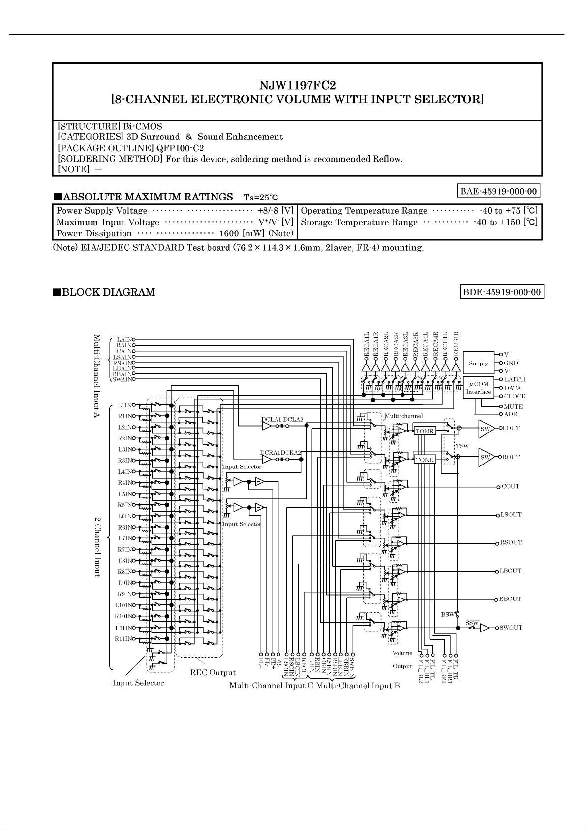
153
AVR3550HD harman/kardon
Page 74

154
AVR3550HD harman/kardon
Page 75

155
AVR3550HD harman/kardon
Page 76

156
AVR3550HD harman/kardon
ST202E
■ ESDPROTECTIONFOR RS-232I/OPINS:
±
15KVHUMANBODYMODEL
■ GUARANTEED120kbpsDATERATE
■ GUARANTEEDSLEWRATERANGE3 to
30V/µs
■ OPERATEFROMA SINGLE5VPOWER
SUPPLY
DESCRIPTION
The ST202E/ST232E are a 2 driver 2 receiver
devices designed for RS-232 and V.28
communications in harsh enviroments. Each
transmitter output and receiver input is protected
against ± 15KV electrostatic discharge (ESD)
shocks. The drivers meet all EIA/TIA-232E and
CCITT V.28 specifications at data rates up to
120Kbps, when loaded in accordance with the
EIA/TIA-232Especification.
The ST202E/232E use a single 5V supply
voltage.
The ST232E operates with four 1µF capacitors,
ST232E
± 15KV ESD PROTECTED
5V RS-232 TRANSCEIVER
N
(PlasticPackage)
(Micro Package)
W
(Micro Package Large)
(TSSOPPackage)
while the ST202E operates with four 0.1µF
capacitors, further reducing cost and board
space.
D
T
ORDERCODES
Typ e Temperature
Range
ST202ECN ST232ECN 0 to 70
ST202EBN ST232EBN -40 to 85
ST202ECD ST232ECD 0 to 70
ST202EBD ST232EBD -40 to 85
ST202ECDR ST232ECDR 0 to 70
ST202EBDR ST232EBDR -40 to 85
ST202ECW ST232ECW 0 to 70
ST202EBW ST232EBW -40 to 85
ST202ECWR ST232ECWR 0 to 70
ST202EBWR ST232EBWR -40 to 85
ST202ECTR ST232ECTR 0 to 70
ST202EBTR ST232EBTR -40 to 85
April 2000
Package Comments
o
C DIP-16 25 parts per tube / 40 tube per box
o
C DIP-16 25 parts per tube / 40 tube per box
o
C SO-16 (Tube) 50 parts per tube / 20 tube per box
o
C SO-16 (Tube) 50 parts per tube / 20 tube per box
o
C SO-16 (Tape& Reel) 2500 parts per reel
o
C SO-16 (Tape& Reel) 2500 parts per reel
o
C SO-16 Large (Tube) 50 parts per tube / 20 tube per box
o
C SO-16 Large (Tube) 50 parts per tube / 20 tube per box
o
C SO-16 Large (Tape & Reel) 1000 partsper reel
o
C SO-16 Large (Tape & Reel) 1000 parts per reel
o
C TSSOP16 (Tape & Reel) 2500 partsper reel
o
C TSSOP16 (Tape & Reel) 2500 parts per reel
1/12
Page 77
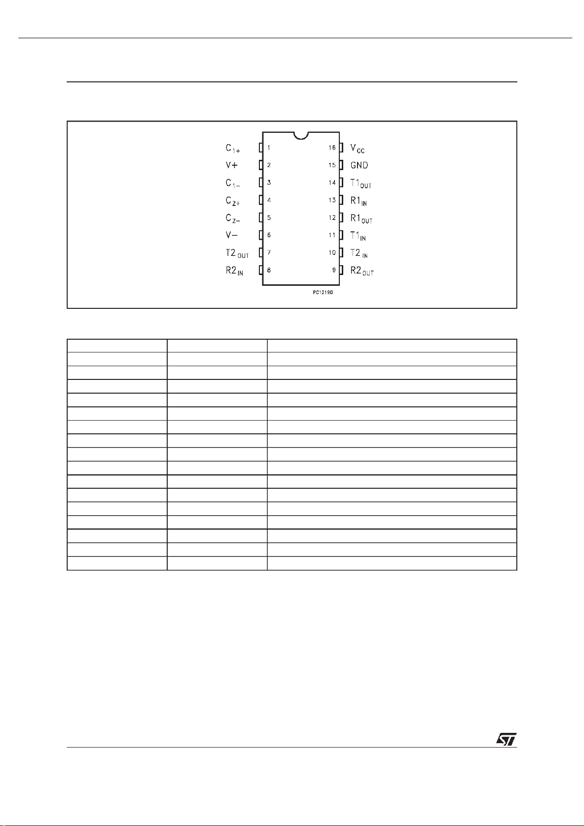
157
AVR3550HD harman/kardon
ST202E/ST232E
PIN CONFIGURATION
PIN DESCRIPTION
PIN No SYM BO L N AME AND F UNCTI O N
1C
2 V+ Doubled Voltage Terminal
3C
4C
5C
6 V- Inverted Voltage Terminal
7T2
8R2
9R2
10 T2
11 T1
12 R1
13 R1
14 T1
15 GND Ground
16 V
+ Positive Terminal for the first Charge Pump Capacitor
1
- Negative Terminal for the first Charge Pump Capacitor
1
+ Positive Terminal for the second Charge Pump Capacitor
2
- Negative Terminal for the second Charge Pump Capacitor
2
OUT
IN
OUT
IN
IN
OUT
IN
OUT
CC
Second Transmitter Output Voltage
Second Receiver Input Voltage
Second Receiver Output Voltage
Second Transmitter Input Voltage
First Transmitter Input Voltage
First Receiver Output Voltage
First Receiver Input Voltage
First Transmitter Output Voltage
Supply Voltage
2/12
Page 78

158
AVR3550HD harman/kardon
Page 79

159
AVR3550HD harman/kardon
M24C64
M24C32
64Kbit and 32Kbit Serial I²C Bus EEPROM
FEATURES SUMMARY
■ Two-Wire I
Supports 400kHz Protocol
■ Single Supply Voltage:
– 4.5 to 5.5V for M24Cxx
– 2.5 to 5.5V for M24Cxx-W
– 1.8 to 5.5V for M24Cxx-R
■ Write Control Input
■ BYTE and PAGE WRITE (up to 32 Bytes)
■ RANDOM and SEQUENTIAL READ Modes
■ Self-Timed Programming Cycle
■ Automatic Address Incr em ent ing
■ Enhanced ESD/Latch-Up Protection
■ More than 1 Million Erase/Write Cycles
■ More than 40-Year Data Retention
Table 1. Product List
Reference Part Number
M24C64
M24C32
2
C Serial Interface
M24C64
M24C64-W
M24C64-R
M24C32
M24C32-W
M24C32-R
Figure 1. Packages
8
1
PDIP8 (BN)
8
1
SO8 (MN)
150 mil width
TSSOP8 (DW)
169 mil width
UFDFPN8 (MB)
2x3mm² (MLP)
1/26January 2005
Page 80
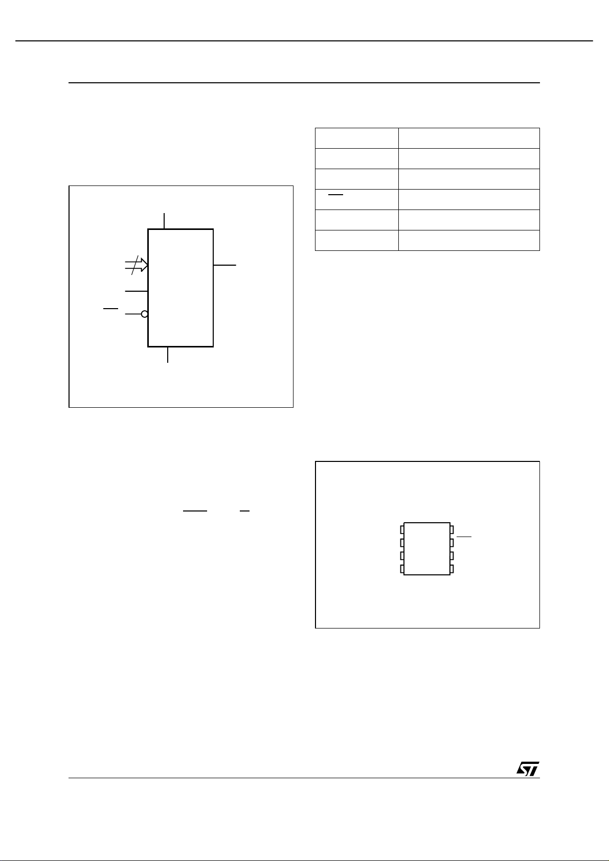
160
AVR3550HD harman/kardon
M24C64, M24C32
SUMMARY DESCRIPTION
These I2C-compatible electrically erasable programmable memory (EEPROM) devices are organized as 8192 x 8 bits (M24C64) and 4096 x 8 bits
(M24C32).
Table 2. Signal Names
E0, E1, E2 Chip Enable
SDA Serial Data
Figure 2. Logic Diagram
V
CC
3
E0-E2 SDA
SCL
WC
2
I
C uses a two-wire serial interf ace, comprisi ng a
M24C64
M24C32
V
SS
AI01844B
bi-directional data line and a clock line. The devices carry a built-in 4-bit Device Type Identifier code
(1010) in accordance with the I
The device behaves as a slave in the I
2
C bus definition.
2
C protocol,
with all memory operations synchronized by the
serial clock. Read and Write operations are initiated by a Start condition, generated by the bus master. The Start condition is followed by a Device
Select Code and Read/Write
bit (RW) (as described in Table 3.), terminated by an acknowledge bit.
When writing data to the memory, the dev ice inserts an acknowled ge bit during the 9
th
bit time,
following the bus master’s 8-bit transmission.
When data is read by the bus master, the bus
master acknowledge s the rec eipt o f the d ata by te
in the same way. Data transfers are terminated by
a Stop condition after an Ack for Write, and after a
NoAck for Read.
SCL Serial Clock
WC
V
CC
V
SS
Power On Reset: V
Write Control
Supply Voltage
Ground
Lock-Out Write Protect
CC
In order to prevent data corruption and inadvertent
Write operations during Power-up, a Power On
Reset (POR) circuit is included . At Power-up, the
internal reset i s he ld a cti ve unti l V
has reached
CC
the Power On Reset (POR) threshold voltage, and
all operations are disabled – the device will not respond to any command. In the sam e way, when
V
drops from the operat ing voltage, below the
CC
Power On Reset (PO R) threshold voltage, a ll operations are disa bled and the device will not respond to any command.
A stable and valid V
(as defined in Table 9. and
CC
Table 10.) must be applied before applying any
logic signal.
Figure 3. DIP, SO, TSSOP and UFDFPN
Connections
M24C64
M24C32
AI01845C
8
CC
7
WCE1
6
SCL
5
SDAV
1
E0 V
2
3
E2
4
SS
Note: See PACKAGE MECHANICAL section for package dimen-
sions, and how to identify pin-1.
4/26
Page 81

161
AVR3550HD harman/kardon
Page 82

3
2
8
3 4
5
3
162
AVR3550HD harman/kardon
NJM2845/46
LOW DROPOUT VOLTAGE REGULATOR
GENERAL DESCRIPTION PACKAGE OUTLINE
The NJM2845 is low dropout voltage regulator. Advanced
Bipolar technology achieves low noise, high ripple rejection
and low quiescent current.
NJM2845 is 3 terminal type and NJM2846 is ON/OFF control
NJM2845DL1
built in type. These product can be selected according to the
applications.
FEATURES
High Ripple Rejection 75dB typ. (f=1kHz,3V Version)
Output Noise Voltage Vno=45µVrms typ. (Vo=3V Version)
Output capacitor with 2.2µF ceramic capacitor (Vo≥2.6V)
Output Current Io(max.)=800mA
High Precision Output Vo ±1.0%
Low Dropout Voltage 0.18V typ. (Io=500mA)
ON/OFF Control (NJM2846)
Internal Short Circuit Current Limit
Internal Thermal Overload Protection
Bipolar Technology
Package Outline TO-252-3 (NJM2845DL1), TO-252-5 (NJM2846DL3)
PIN CONFIGURATION
NJM2846DL3
1.V
IN
2.GND
3.V
OUT
1.CONTROL
2.V
IN
3.GND
4.Vo
1
1 2
5.NC
NJM2845DL1 NJM2846DL3
EQUIVALENT CIRCUIT
V
GND
IN
Thermal
Protection
Bandgap
Reference
V
OUT
V
IN
Control
GND
NJM2845DL1
Bandgap
Reference
NJM2
Thermal
Protection
46DL3
V
OUT
Ver.2005-01-20
Page 83

163
AVR3550HD harman/kardon
Page 84

164
AVR3550HD harman/kardon
Page 85

165
AVR3550HD harman/kardon
8 Mbit SPI Serial Flash
SST25VF080B
SST25VF080B8Mb Serial Peripheral Interface (SPI) flash memory
FEATURES:
Data Sheet
• Single Voltage Read and Write Operations
– 2.7-3.6V
• Serial Interface Architecture
– SPI Compatible: Mode 0 and Mode 3
• High Speed Clock Frequency
–50 MHz
• Superior Reliability
– Endurance: 100,000 Cycles (typical)
– Greater than 100 years Data Retention
• Low Power Consumption:
– Active Read Current: 10 mA (typical)
– Standby Current: 5 µA (typical)
• Flexible Erase Capability
– Uniform 4 KByte sectors
– Uniform 32 KByte overlay blocks
– Uniform 64 KByte overlay blocks
• Fast Erase and Byte-Program:
– Chip-Erase Time: 35 ms (typical)
– Sector-/Block-Erase Time: 18 ms (typical)
– Byte-Program Time: 7 µs (typical)
• Auto Address Increment (AAI) Programming
– Decrease total chip programming time over
Byte-Program operations
• End-of-Write Detection
– Software polling the BUSY bit in Status Register
– Busy Status readout on SO pin in AAI Mode
• Hold Pin (HOLD#)
– Suspends a serial sequence to the memory
without deselecting the device
• Write Protection (WP#)
– Enables/Disables the Lock-Down function of the
status register
• Software Write Protection
– Write protection through Block-Protection bits in
status register
• Temperature Range
– Commercial: 0°C to +70°C
– Industrial: -40°C to +85°C
• Packages Available
– 8-lead SOIC (200 mils)
– 8-contact WSON (6mm x 5mm)
• All non-Pb (lead-free) devices are RoHS compliant
PRODUCT DESCRIPTION
SST’s 25 series Serial Flash family features a four-wire,
SPI-compatible interface that allows for a low pin-count
package which occupies less board space and ultimately
lowers total system costs. The SST25VF080B devices are
enhanced with improved operating frequency and even
lower power consumption than the original SST25VFxxxA
devices. SST25VF080B SPI serial flash memories are
manufactured with SST’s proprietary, high-performance
CMOS SuperFlash technology. The split-gate cell design
and thick-oxide tunneling injector attain better reliability and
manufacturability compared with alternate approaches.
The SST25VF080B devices significantly improve performance and reliability, while lowering power consumption.
The devices write (Program or Erase) with a single power
supply of 2.7-3.6V for SST25VF080B. The total energy
consumed is a function of the applied voltage, current, and
time of application. Since for any given voltage range, the
SuperFlash technology uses less current to program and
has a shorter erase time, the total energy consumed during
any Erase or Program operation is less than alternative
flash memory technologies.
The SST25VF080B device is offered in both 8-lead SOIC
(200 mils) and 8-contact WSON (6mm x 5mm) packages.
See Figure 1 for pin assignments.
Page 86

166
AVR3550HD harman/kardon
8 Mbit SPI Serial Flash
SST25VF080B
Data Sheet
FUNCTIONAL BLOCK DIAGRAM
SuperFlash
Address
Buffers
and
Latches
X - Decoder
Memory
Y - Decoder
Control Logic
CE#
I/O Buffers
and
Data Latches
Serial Interface
1296 B1.0
SCK SI SO WP# HOLD#
©2006 Silicon Storage Technology, Inc. S71296-01-000 1/06
Page 87

167
AVR3550HD harman/kardon
8 Mbit SPI Serial Flash
SST25VF080B
Data Sheet
PIN DESCRIPTION
CE#
SO
WP#
V
SS
1
2
Top View
3
4
1296 08-soic S2A P1.0
8
V
DD
7
HOLD#
6
SCK
5
SI
CE#
SO
WP#
V
SS
1
2
Top View
3
4
1296 08-wson QA P2.0
8
7
6
5
V
DD
HOLD#
SCK
SI
8-LEAD SOIC 8-CONTACT WSON
FIGURE 1: PIN ASSIGNMENTS
TABLE 1: PIN DESCRIPTION
Symbol Pin Name Functions
SCK Serial Clock To provide the timing of the serial interface.
Commands, addresses, or input data are latched on the rising edge of the clock input,
while output data is shifted out on the falling edge of the clock input.
SI Serial Data Input To transfer commands, addresses, or data serially into the device.
Inputs are latched on the rising edge of the serial clock.
SO Serial Data Output To transfer data serially out of the device.
Data is shifted out on the falling edge of the serial clock.
Outputs Flash busy status during AAI Programming when reconfigured as RY/BY# pin.
See “Hardware End-of-Write Detection” on page 12 for details.
CE# Chip Enable The device is enabled by a high to low transition on CE#. CE# must remain low for the
duration of any command sequence.
WP# Write Protect The Write Protect (WP#) pin is used to enable/disable BPL bit in the status register.
HOLD# Hold To temporarily stop serial communication with SPI flash memory without resetting the
device.
V
DD
V
SS
Power Supply To provide power supply voltage: 2.7-3.6V for SST25VF080B
Ground
T1.0 1296
©2006 Silicon Storage Technology, Inc. S71296-01-000 1/06
Page 88

168
AVR3550HD harman/kardon
Page 89

169
AVR3550HD harman/kardon
Page 90

170
AVR3550HD harman/kardon
Page 91

171
AVR3550HD harman/kardon
Page 92

172
AVR3550HD harman/kardon
Page 93

173
AVR3550HD harman/kardon
Page 94

174
AVR3550HD harman/kardon
Page 95
175
AVR3550HD harman/kardon
Page 96

176
AVR3550HD harman/kardon
NJM2595
5-INPUT 3-OUTPUT VIDEO SWITCH
■ GENERAL DESCRIPTION ■ PACKAGE OUTLINE
The NJM2595 is a 5-input 3-output video switch. Its switches
select one from five signals received from VTR,TV,DVD,
TV-GAME and others.
The NJM2595 is designed for audio items, such as AV amplifier
and others.
NJM2595D NJM2595M
■ FEATURES
● 5-input 3-output
● Operating Voltage ±4.0 to ±6.5V
● Operating current ±15mAtyp. at Vcc=±5V
● Crosstalk -65dBtyp.
● Internal 6dB Amplifier
● Internal 75Ω Driver
● Bipolar Technology
● Package Outline DIP16,DMP16
■ PIN CONFIGURATION and BLOCK DIAGRAM
16
+
SW2V
10 14 2
SW1
SW5
Vin1
Vin2
Vin3
Vin4
Vin5
13
20k
20k
20k
S5
S6
S7
6dB
Amp
6dB
Amp
6dB
Amp
8 12 6 4
-
75Ω
Driver
75Ω
Driver
75Ω
Driver
1
15
11
Vout1
Vout2
Vout3
9
20k
7
20k
5
3
20k
20k
S2
S3
SW3
S4
SW4
S1
GND V
Page 97

177
AVR3550HD harman/kardon
NJM2595
■ EQUIVALENT CIRCUIT
PIN No. PIN NAME INSIDE EQUIVALENT CIRCUIT VOLTAGE
16 V+ 5V
8 V- -5V
12 GND 13
9
7
5
3
1
15
11
Vin1
Vin2
Vin3
Vin4
Vin5
Vout1
Vout2
Vout3
Vin
Vcc
260
2.1k
20k
Gnd
Vcc
Vee
Vout
0V
0V
4
6
2
Vee
SW3
SW4
SW5
SW
20k
16k
Vcc
-
8k
4k
Gnd
Vee
Page 98

178
AVR3550HD harman/kardon
NJM2595
■ EQUIVALENT CIRCUIT
PIN No. PIN NAME INSIDE EQUIVALENT CIRCUIT VOLTAGE
14
10
■ TEST CIRCUIT
V
SW1
SW2
+
Vout2.2 Vout2.1
SW
32k
16k
20k
Gnd
Vout3.2
Vcc
4k
Vee
Vout3.1
-
0.1µF
V
Vout2
SW5
SW5
V
CL
CH
75
Ω
+
75
100µF
16 15 14 13 12 11
+
V
Vout1
1
75
Ω
75
Ω
Ω
V
CL
+
V
SW1
SW1
Vin5
10µF
75
CH
Vin5
Ω
V
75
Ω
Vin1
10µF
+
Vin1
SW3
+
SW3
V
CL
CH
GND
Vin4
10µF
Vin4
75
Ω
75
75
V
+
9
-
V
8765432
75
Vin2
10µF
Vin2
0.1µF
Ω
+
100µF
10
+
V
SW2
SW2
Vin3
10µF
75
CH
Vin3
Ω
V
Vout3
SW4
SW4
V
CL
CH
Ω
Ω
CL
Vout1.2 Vout1.1
-
V
Page 99

179
AVR3550HD harman/kardon
NJM2068M (OP-AMP)
Page 100

180
AVR3550HD harman/kardon
IC86
AVR347 harman/kardon
 Loading...