

Page 1
130
AVR354 harman/kardon
MK2302S-01
Multiplier and Zero Delay Buffer
Description
The MK2302S-01is a high performance Zero Delay
Buffer (ZDB) which integrates ICS’ proprietary
analog/digital Phase Locked Loop (PLL) techniques.
The chip is part of ICS’ ClockBlocksTM family and was
designed as a performance upgrade to meet today’s
higher speed and lo wer voltage requirements. The zero
delay feature means that the rising edge of the input
clock aligns with the rising edges of both output clocks,
giving the appearance of no delay through the device.
There are two outputs on the chip , one being a
low-skew divide by two of the other output.
The MK2302S-01 is ideal for synchronizing outputs in a
large variety of systems, from personal computers to
data communications to graphics/video. By allowing
off-chip feedback paths, the device can eliminate the
delay through other devices.
Features
• 8 pin SOIC package
• Low input to output skew of 250ps max
• Absolute jitter ± 500ps
• Propagation Delay ± 350ps
• Ability to choose between different multipliers from
0.5X to 16X
• Output clock frequency up to 133 MHz at 3.3V
• Can recover degraded input clock duty cycle
• Output clock duty cycle of 45/55
• Full CMOS clock swings with 25mA drive capability
at TTL levels
• Advanced, low power CMOS process
• Operating voltage of 3.3V or 5V
• Industrial temperature version available
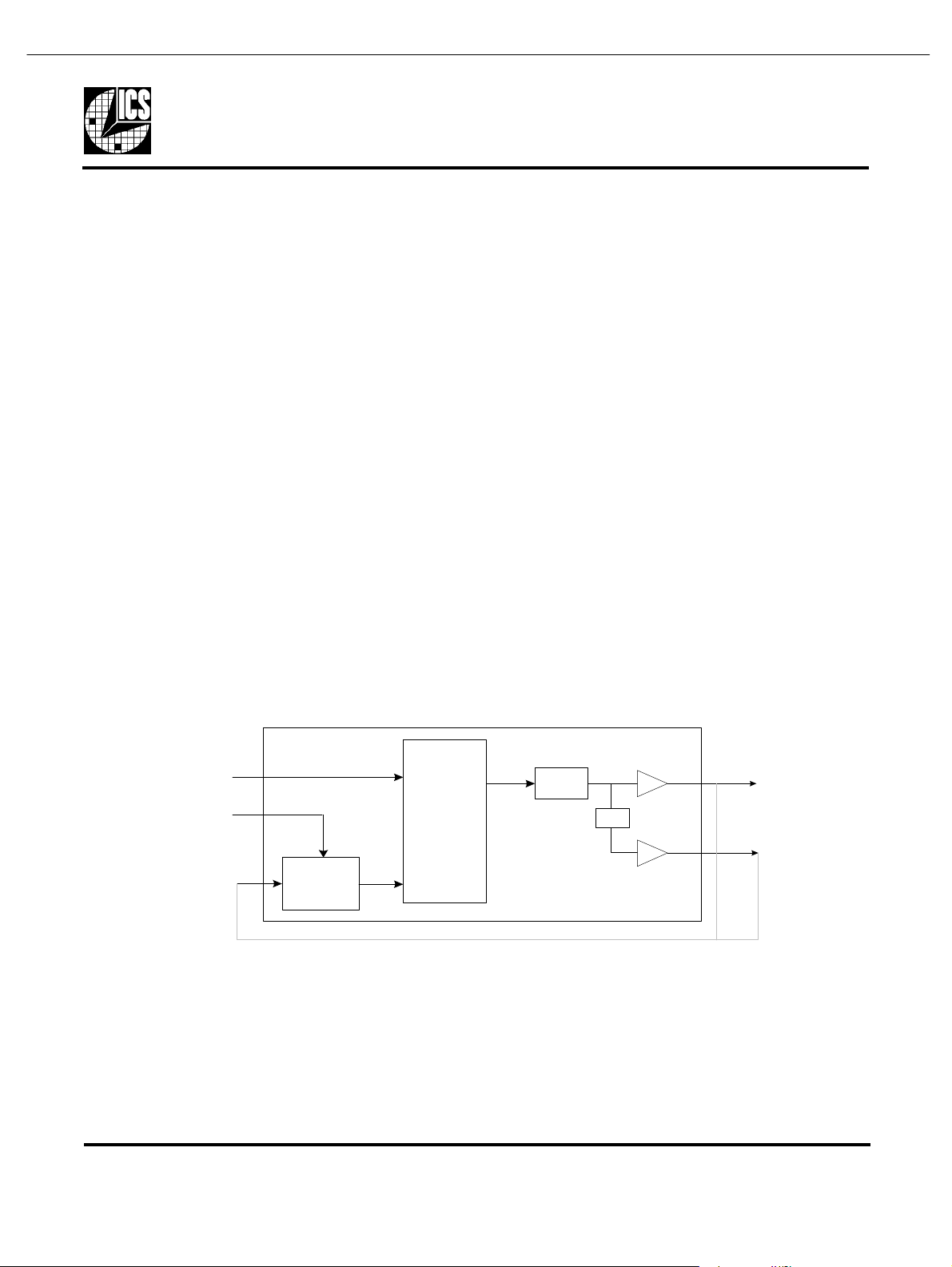
Block Diagram
IC L K
S1:0
FBIN
Phase
Detector,
Charge
Pump,
and Loop
divide
by N
External feedback can come from CLK1 or CLK2 (see table on page 2)
Filter
VCO
/2
CLK1
CLK2
MDS 2302S-01 B
Integrated Circuit Systems, Inc.
● 525 Race Street, San Jose, CA 95126 ● tel (408 ) 295-9800 ● www.icst.com
Page 2
Multiplier and Zero Delay Buffer
MK2302S-01
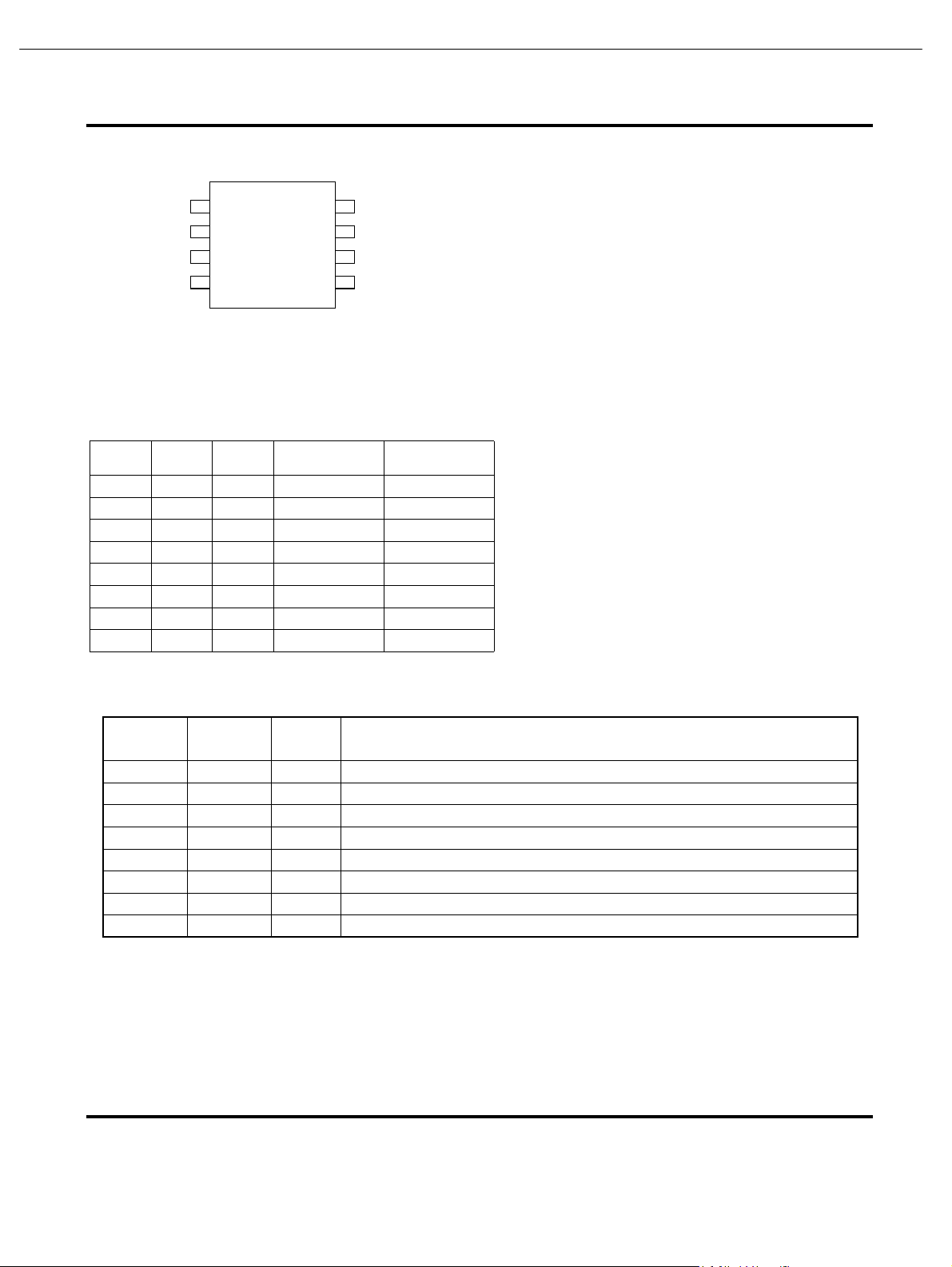
Pin Assignment
Clock Multiplier Decoding Table 1
(Multiplies Input clock by shown amount)
Pin Descriptions
FBIN
ICLK
GND
VDD
S0
CLK1
CLK21
2
3
4
8
7
6
5
GND
S1
1
2
3
4
8
7
6
5
8 pin (150 mil) SOIC
FBIN S1 S0 CLK1 CLK2
CLK1 0 0 2 X ICLK ICLK
CLK1 0 1 4 X ICLK 2 X ICLK
CLK1 1 0 ICLK ICLK/2
CLK1 1 1 8 X ICLK 4 X ICLK
CLK2 0 0 4 X ICLK 2 X ICLK
CLK2 0 1 8 X ICLK 4 X ICLK
CLK2 1 0 2 X ICLK ICLK
CLK2 1 1 16 X ICLK 8 XICLK
Pin
Number
Pin
Name
Pin
Type
Pin Description
1 FBIN Input Feedback clock input.
2 ICLK Input Reference clock input.
3 GND Power Connect to ground.
4 S0 Input Select 0 for output clock per decoding table above. Pull-up.
5 S1 Input Select 1 for output clock per decoding table above. Pull up.
6 CLK1 Output Clock output per table above.
7 VDD Power Connect to +3.3V or +5.0V.
8 CLK2 Output Clock output per table above. Low skew divide by two of pin 6 clock.
131
AVR354 harman/kardon
MDS 2302S-01 B
Integrated Circuit Systems, Inc. ● 525 Race Str eet, San Jose, CA 95126 ● tel (408) 295 -9800 ● www.icst.com
Page 3
Multiformat Video Encoder
Six, 11-Bit, 297 MHz DACs
ADV7342/ADV7343
Rev. 0
Information furnished by Analog Devices is believed to be accurate and reliable. However, no
responsibility is assumed by Anal og Devices for its use, nor for any infringements of patents or ot her
rights of third parties that may result from its use. Specifications subject to change without notice. No
license is granted by implication or otherwise under any patent or patent rights of Analog Devices.
Trademarks and registered trademarks are the property of their respective owners.
One Technology Way, P.O. Box 9106, Norwood, MA 02062-9106, U.S.A.
Tel: 781.329.4700 www.analog.com
Fax: 781.461.3113 ©2006 Analog Devices, Inc. All rights reserved.
FEATURES
74.25 MHz 20-/30-bit high definition input support
Compliant with SMPTE 274M (1080i), 296M (720p),
and 240M (1035i)
6, 11-bit, 297 MHz video DACs
16× (216 MHz) DAC oversampling for SD
8× (216 MHz) DAC oversampling for ED
4× (297 MHz) DAC oversampling for HD
37 mA maximum DAC output current
NTSC M, PAL B/D/G/H/I/M/N, PAL 60 support
NTSC and PAL square pixel operation (24.54 MHz/29.5 MHz)
Multiformat video input support
4:2:2 YCrCb (SD, ED, and HD)
4:4:4 YCrCb (ED and HD)
4:4:4 RGB (SD, ED, and HD)
Multiformat video output support
Composite (CVBS) and S-Video (Y/C)
Component YPrPb (SD, ED, and HD)
Component RGB (SD, ED, and HD)
Macrovision® Rev 7.1.L1 (SD) and Rev 1.2 (ED) compliant
Simultaneous SD and ED/HD operation
EIA/CEA-861B compliance support
Programmable features
Luma and chroma filter responses
Vertical blanking interval (VBI)
Subcarrier frequency (F
SC
) and phase
Luma delay
Copy generation management system (CGMS)
Closed captioning and wide screen signaling (WSS)
Integrated subcarrier locking to external video source
Complete on-chip video timing generator
On-chip test pattern generation
On-board voltage reference (optional external input)
Serial MPU interface with dual I
2
C® and SPI® compatibility
3.3 V analog operation
1.8 V digital operation
3.3 V I/O operation
Temperature range: −40°C to +85°C
APPLICATIONS
DVD recorders and players
High definition Blu-ray DVD players
HD-DVD players
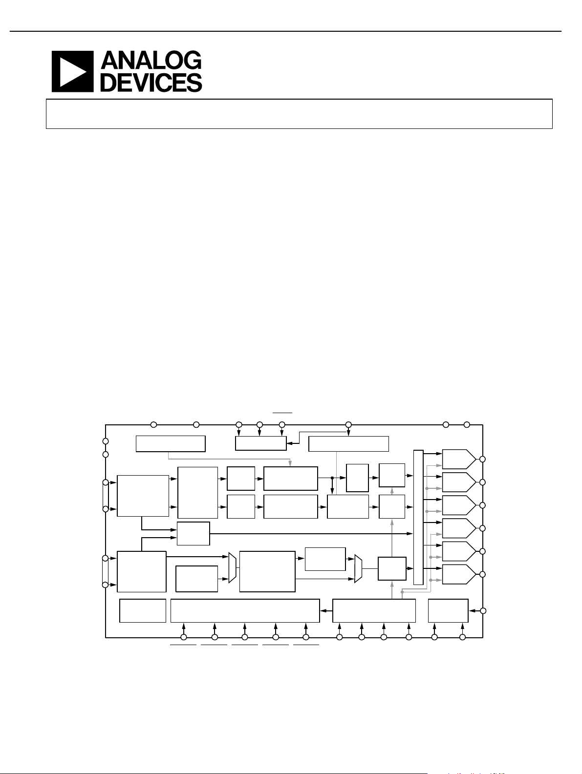
FUNCTIONAL BLOCK DIAGRAM
R
GND_IO
VDD_IO
10-BIT
SD
VIDEO
DATA
20-BIT
ED/HD
VIDEO
DATA
S_HSYNCP_HSYNC P_VSYNC P_BLANK S_VSYNC
11-BIT
DAC 1
DAC 1
11-BIT
DAC 2
DAC 2
11-BIT
DAC 3
DAC 3
11-BIT
DAC 4
DAC 4
11-BIT
DAC 5
DAC 5
11-BIT
DAC 6
DAC 6
MULTIPLEXER
REFERENCE
AND CABLE
DETECT
16x/4x OVERSAM PLING
DAC PLL
VIDEO TI MING GENERATOR
POWER
MANAGEMENT
CONTRO L
CLKIN (2) PV
DD
PGND EXT_LF (2) V
REF
COMP (2)
R
SET
(2)
ED/HD INPUT
DEINTERLEAVE
PROGRAMMABLE
HDTV FILTERS
SHARPNESS AND
ADAPTIVE FILTER
CONTROL
YCbCr
HDTV
TEST
PATTERN
GENERATOR
YCbCr
TO
RGB MATRIX
G/B
RGB
ASYNC
BYPASS
RGB
DGND (2) VDD (2)
SCL/
MOSI
SDA/
SCLK
A
LSB/
SPI_SS
SFL/
MISO
MPU PORT
SUBCARRIER FREQUENCY
LOCK (SFL )
YUV
TO
YCrCb/
RGB
PROGRAMMABLE
CHROMINANCE
FILTER
ADD
BURST
RGB/YCrCb
TO
YUV
MATRIX
4:2:2 TO 4: 4:4
HD DDR
DEINTERLEAVE
SIN/COS DDS
BLOCK
16×
FILTER
16×
FILTER
4×
FILTER
AGND
V
AA
ADD
SYNC
VBI DATA SERVICE
INSERTION
PROGRAMMABLE
LUMINANCE
FILTER
06399-001
ADV7342/ADV7343
Figure 1.
Protected by U.S. Patent Numbers 5,343,196 and 5,442,355 and other intellectual property rights.
Protected by U.S. Patent Numbers 4,631,603, 4,577,216, 4,819,098 and other intellectual property rights.
132
AVR354 harman/kardon
Page 4
ADV7342/ADV7343
Rev. 0 | Page 18 of 88
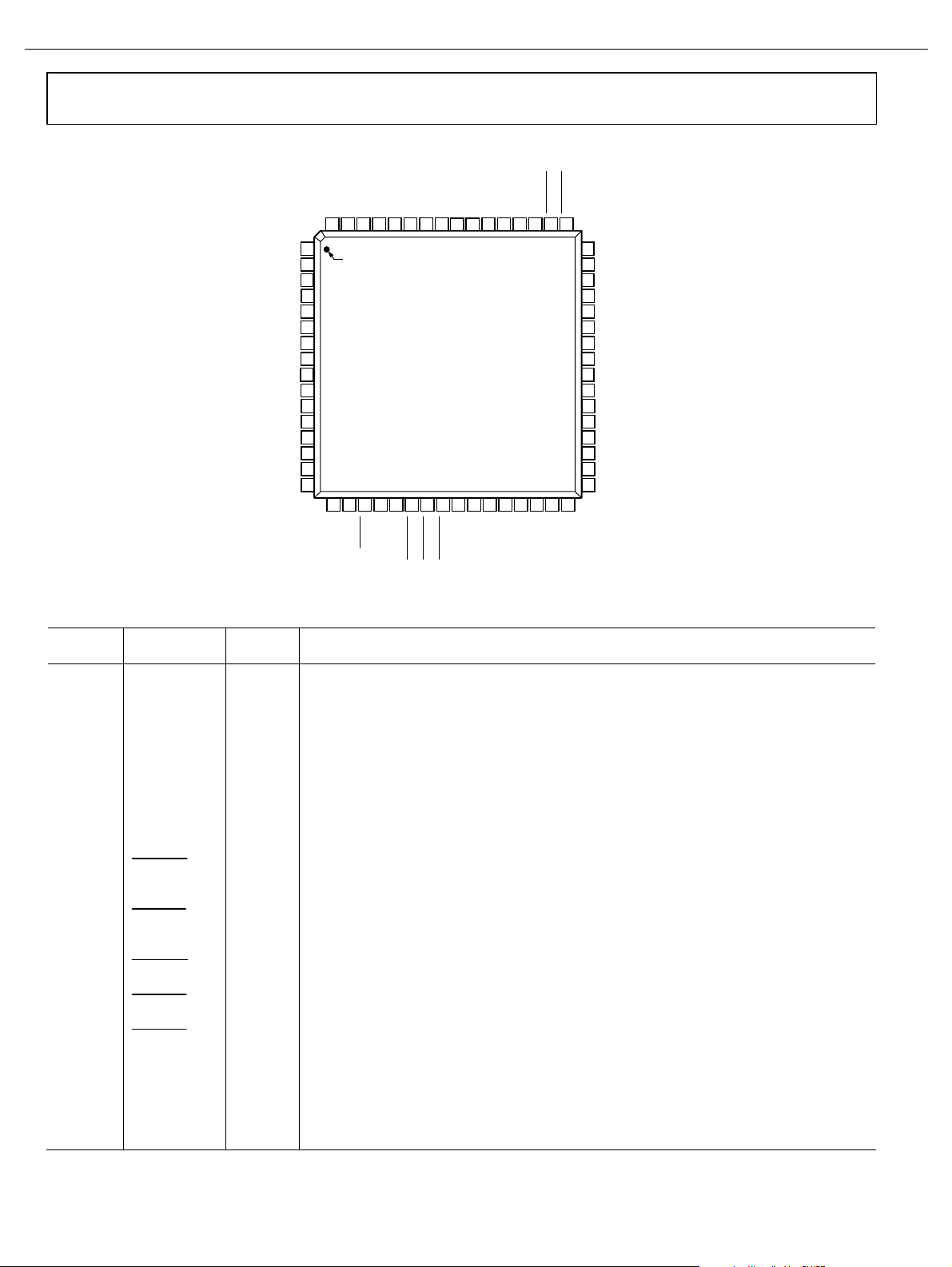
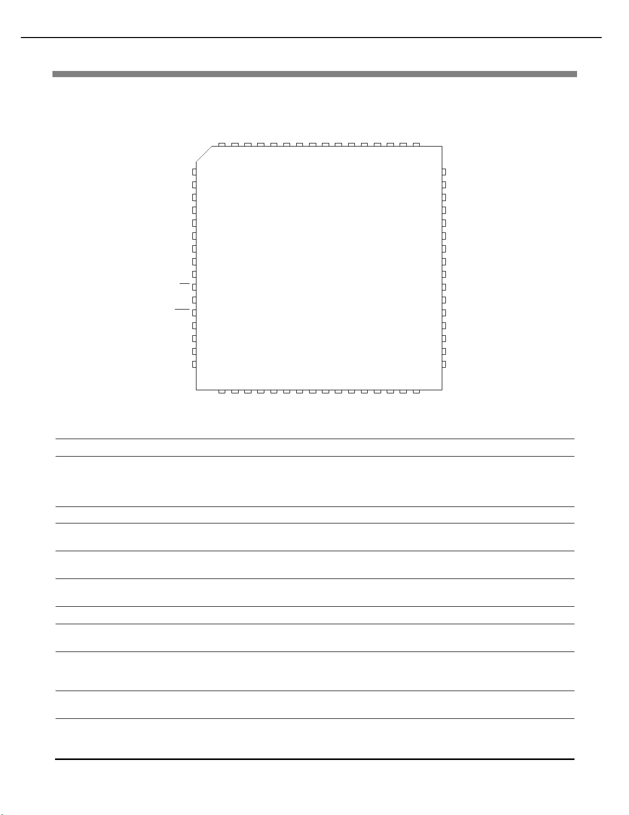
PIN CONFIGURATION AND FUNCTION DESCRIPTIONS
64
GND_IO63CLKIN_B62S761S660S559S458S357DGND56V
DD
55S254S153S052
TEST551TEST450S_HSYNC49S_VSYNC
47
R
SET1
46
V
REF
45
COMP1
42
DAC 3
43
DAC 2
44
DAC 1
48
SFL/MISO
41
V
AA
40
AGND
39
DAC 4
37
DAC 6
36
R
SET2
35
COMP2
34
PV
DD
33
EXT_LF1
38
DAC 5
2
TEST0
3
TEST1
4
Y0
7
Y3
6
Y2
5
Y1
1
V
DD_IO
8
Y4
9
Y5
10
V
DD
12
Y6
13
Y7
14
TEST2
15
TEST3
16
C0
11
DGND
17C118C219
ALSB/SPI_SS
20
SDA/SCLK
21
SCL/MOSI
22 23
P_HSYNC
24
P_VSYNC
25
P_BLANK
26
C4
C327C528C629C7
30
CLKIN_A
31 32
PGND
PIN 1
ADV7342/ADV7343
TOP VIEW
(Not to Scale)
EXT_LF2
06399-021
Figure 21. Pin Configuration
Table 13. Pin Function Descriptions
Pin No. Mnemonic
Input/
Output
Description
13, 12,
9 to 4
Y7 to Y0 I 8-Bit Pixel Port. Y0 is the LSB. Refer to Table 31 for input modes.
29 to 25,
18 to 16
C7 to C0 I 8-Bit Pixel Port. C0 is the LSB. Refer to Table 31 for input modes.
62 to 58,
55 to 53
S7 to S0 I 8-Bit Pixel Port. S0 is the LSB. Refer to Table 31 for input modes.
52, 51, 15,
14, 3, 2
TEST5 to
TEST0
I Unused. These pins should be connected to DGND.
30 CLKIN_A I Pixel Clock Input for HD Only (74.25 MHz), ED1 Only (27 MHz or 54 MHz) or SD Only (27 MHz).
63 CLKIN_B I
Pixel Clock Input for Dual Modes Only. Requires a 27 MHz reference clock for ED operation or a
74.25 MHz reference clock for HD operation.
50
S_HSYNC
I/O
SD Horizontal Synchronization Signal. This pin can also be configured to output an SD, ED, or HD
horizontal synchronization signal. See the External Horizontal and Vertical Synchronization
Control section.
49
S_VSYNC
I/O
SD Vertical Synchronization Signal. This pin can also be configured to output an SD, ED, or HD
vertical synchronization signal. See the External Horizontal and Vertical Synchronization Control
section.
22
P_HSYNC
I
ED/HD Horizontal Synchronization Signal. See the External Horizontal and Vertical
Synchronization Control section.
23
P_VSYNC
I
ED/HD Vertical Synchronization Signal. See the External Horizontal and Vertical Synchronization
Control section.
24
P_BLANK
I ED/HD Blanking Signal. See the External Horizontal and Vertical Synchronization Control section.
48 SFL/MISO I/O
Multifunctional Pin: Subcarrier Frequency Lock (SFL) Input/SPI Data Output. The SFL input is
used to drive the color subcarrier DDS system, timing reset, or subcarrier reset.
47 R
SET1
I
This pin is used to control the amplitudes of the DAC 1, DAC 2, and DAC 3 outputs. For full-drive
operation (for example, into a 37.5 Ω load), a 510 Ω resistor must be connected from R
SET1
to
AGND. For low drive operation (for example, into a 300 Ω load), a 4.12 kΩ resistor must be
connected from R
SET1
to AGND.
133
AVR354 harman/kardon
Page 5
ADV7342/ADV7343
Rev. 0 | Page 19 of 88
Pin No. Mnemonic
Input/
Output Description
36 R
SET2
I
This pin is used to control the amplitudes of the DAC 4, DAC 5, and DAC 6 outputs. A 4.12 kΩ
resistor must be connected from R
SET2
to AGND.
45, 35
COMP1,
COMP2
O Compensation Pins. Connect a 2.2 nF capacitor from both COMP pins to V
AA
.
44, 43, 42
DAC 1, DAC 2,
DAC 3
O DAC Outputs. Full and low drive capable DACs.
39, 38, 37
DAC 4, DAC 5,
DAC 6
O DAC Outputs. Low drive only capable DACs.
21 SCL/MOSI I Multifunctional Pin: I2C Clock Input/SPI Data Input.
20 SDA/SCLK I/O Multifunctional Pin: I2C Data Input/Output. Also, SPI clock input.
19
ALSB/SPI_SS
I Multifunctional Pin: This signal sets up the LSB
2
of the MPU I2C address. Also, SPI slave select.
46 V
REF
Optional External Voltage Reference Input for DACs or Voltage Reference Output.
41 VAA P Analog Power Supply (3.3 V).
10, 56 VDD P
Digital Power Supply (1.8 V). For dual-supply configurations, V
DD
can be connected to other 1.8 V
supplies through a ferrite bead or suitable filtering.
1 V
DD_IO
P Input/Output Digital Power Supply (3.3 V).
34 PVDD P
PLL Power Supply (1.8 V). For dual-supply configurations, PV
DD
can be connected to other 1.8 V
supplies through a ferrite bead or suitable filtering.
33 EXT_LF1 I External Loop Filter for On-Chip PLL 1.
31 EXT_LF2 I External Loop Filter for On-Chip PLL 2.
32 PGND G PLL Ground Pin.
40 AGND G Analog Ground Pin.
11, 57 DGND G Digital Ground Pin.
64 GND_IO G Input/Output Supply Ground Pin.
1
ED = enhanced definition = 525p and 625p.
2
LSB = least significant bit. In the ADV7342, setting the LSB to 0 sets the I2C address to 0xD4. Setting it to 1 sets the I2C address to 0xD6. In the ADV7343, setting the
LSB to 0 sets the I2C address to 0x54. Setting it to 1 sets the I2C address to 0x56.
134
AVR354 harman/kardon
Page 6
135
AVR354 harman/kardon
Page 7
136
AVR354 harman/kardon
IC51 XM IC
Page 8
137
AVR354 harman/kardon
Page 9
138
AVR354 harman/kardon
Page 10
139
AVR354 harman/kardon
Page 11
140
AVR354 harman/kardon
Page 12
141
AVR354 harman/kardon
Page 13
142
AVR354 harman/kardon
Page 14
143
AVR354 harman/kardon
Page 15
144
AVR354 harman/kardon
Page 16
145
AVR354 harman/kardon
Page 17
146
AVR354 harman/kardon
Page 18
147
AVR354 harman/kardon
Page 19
148
AVR354 harman/kardon
Page 20
149
AVR354 harman/kardon
5V POWERED MULTI-CHANNEL
RS-232 DRIVERS AND RECEIVERS
■ SUPPLYVOLTAGERANGE:4.5TO 5.5V
■
SUPPLYCURRENT NOLOAD(TYP):5mA
■ TRANSMITTEROUTPUTVOLTAGESWING
(TYP):±7.8V
■
CONTROLLEDOUTPUTSLEWRATE
■ RECEIVERINPUTVOLTAGERANGE:
■
DATARATE(TYP):220Kbps
■ OPERATINGTEMPERATURERAN GE:
-40TO85
■
COMPATIBLEWITH MAX232ANDMAX202
o
C,0 TO70oC
DESCRIPTION
The ST232 is a 2 driver, 2 receiver device
following EIA/TIA-232 and V.28 communication
standard. It is particularly suitable for applications
where ±12V is not available. The ST232 uses a
single 5V power supply and only four external
capacitors (0.1µF). Typical applications are in:
Portable Computers, Low Power Modems,
Interfaces Translation, Battery Powered RS-232
System,Multi-Drop RS-232 Networks.
±30V
ST232
N
(PlasticPackage)
(Micro Package)
W
(Micro PackageLarge)T(TSSOPPackage)
D
ORDERCODES
Type Temperature
ST232CN 0 to 70
ST232BN -40 to 85
ST232CD 0 to 70
ST232BD -40 to 85
ST232CDR 0 to 70
ST232BDR -40 to 85
ST232CW 0 to 70
ST232BW -40 to 85
ST232CWR 0 to 70
ST232BWR -40 to 85
ST232CT 0 to 70
ST232BT -40 to 85
ST232CTR 0 to 70
ST232BTR -40 to 85
February 2001
Package Commen ts
Rang e
o
C DIP-16 25 parts per tube / 40 tubeper box
o
C DIP-16 25 parts per tube / 40 tubeper box
o
C SO-16 (Tube) 50 parts per tube / 20 tubeper box
o
C SO-16 (Tube) 50 parts per tube / 20 tube per box
o
C SO-16 (Tape& Reel) 2500 parts per reel
o
C SO-16 (Tape & Reel) 2500 parts per reel
o
C SO-16 Large (Tube) 49 parts per tube / 25 tubeper box
o
C SO-16 Large (Tube) 49 parts per tube / 25 tubeper box
o
C SO-16 Large (Tape & Reel) 1000 parts per reel
o
C SO-16 Large (Tape & Reel) 1000 parts per reel
o
C TSSOP16 (Tube) only for samples
o
C TSSOP16 (Tube) only for samples
o
C TSSOP16 (Tape & Reel) 2500 parts per reel
o
C TSSOP16 (Tape & Reel) 2500 parts per reel
1/11
Page 21
150
AVR354 harman/kardon
ST232
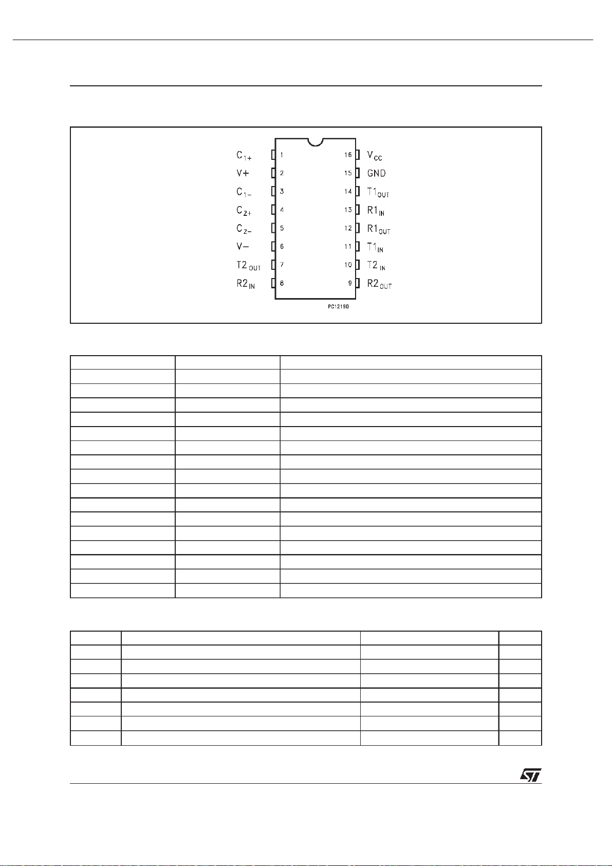
PIN CONFIGURATION
PIN DESCRIPTION
PIN No SYMBOL NAME AND F UNC T I O N
1C
+ Positive Terminal forthe first Charge Pump Capacitor
1
2 V+ Doubled Voltage Terminal
3C
4C
5C
- Negative Terminal for the first Charge Pump Capacitor
1
+ Positive Terminal forthe second Charge Pump Capacitor
2
- Negative Terminal for the second Charge Pump Capacitor
2
6 V- Inverted Voltage Terminal
7T2
8R2
9R2
10 T2
11 T1
12 R1
13 R1
14 T1
OUT
IN
OUT
IN
IN
OUT
IN
OUT
Second Transmitter Output Voltage
Second Receiver Input Voltage
Second Receiver Output Voltage
Second Transmitter Input Voltage
First Transmitter Input Voltage
First Receiver Output Voltage
First Receiver Input Voltage
First Transmitter Output Voltage
15 GND Ground
16 V
CC
Supply Voltage
ABSOLUTE MAXIMUM RATINGS(Note1)
Symb o l Para met er Val u e Unit
V
T
R
T
OUT
R
OUT
T
SCTOUT
T
AbsoluteMaximum Ratingsarethosevalues beyond whichdamage tothedevicemayoccur. Functionaloperationundertheseconditionisnot implied.
Note1:Noexternal supply can be appliedtoV+ terminalandV- terminal.
2/11
Supply Voltage -0.3 to 6 V
CC
Transmitter Input Voltage Range -0.3 to (VCC+ 0.3) V
IN
Receiver Input Voltage Range ±30 V
IN
Transmitter Output Voltage Range (V+ + 0.3) to (V- - 0.3) V
Receiver Output Voltage Range -0.3 to (VCC+ 0.3) V
Short Circuit Duration on T
Storage Temperature Range -65 to +150
stg
OUT
infinite
o
C
Page 22
151
AVR354 harman/kardon
M24C64
M24C32
64Kbit and 32Kbit Serial I²C Bus EEPROM
FEATURES SUMMARY
M24C64
M24C32
2
C Serial Interface
M24C64
M24C64-W
M24C64-R
M24C32
M24C32-W
M24C32-R
■ Two-Wire I
Supports 400kHz Protocol
■ Single Supply Voltage:
– 4.5 to 5.5V for M24Cxx
– 2.5 to 5.5V for M24Cxx-W
– 1.8 to 5.5V for M24Cxx-R
■ Write Control Input
■ BYTE and PAGE WRITE (up to 32 Bytes)
■ RANDOM and SEQUENTIAL READ Modes
■ Self-Timed Programming Cycle
■ Automatic Address Incrementing
■ Enhanced ESD/Latch-Up Protection
■ More than 1 Million Erase/Write Cycles
■ More than 40-Year Data Retention
Table 1. Product List
Reference Part Number
Figure 1. Packages
8
1
PDIP8 (BN)
8
1
SO8 (MN)
150 mil width
TSSOP8 (DW)
169 mil width
UFDFPN8 (MB)
2x3mm² (MLP)
1/26January 2005
Page 23
152
AVR354 harman/kardon
M24C64, M24C32
SUMMARY DESCRIPTION
These I2C-compatible electrically erasable programmable memory (EEPROM) devices are organized as 8192 x 8 bits (M24C64) and 4096 x 8 bits
(M24C32).
Table 2. Signal Names
E0, E1, E2 Chip Enable
SDA Serial Data
Figure 2. Logic Diagram
V
CC
3
E0-E2 SDA
SCL
WC
2
I
C uses a two-wire serial interf ace, comprisi ng a
M24C64
M24C32
V
SS
AI01844B
bi-directional data line and a clock line. The devices carry a built-in 4-bit Device Type Identifier code
(1010) in accordance with the I
The device behaves as a slave in the I
2
C bus definition.
2
C protocol,
with all memory operations synchronized by the
serial clock. Read and Write operations are initiated by a Start condition, generated by the bus master. The Start condition is followed by a Device
Select Code and Read/Write
bit (RW) (as described in Table 3.), terminated by an acknowledge bit.
When writing data to the memory, the dev ice inserts an acknowled ge bit during the 9
th
bit time,
following the bus master’s 8-bit transmission.
When data is read by the bus master, the bus
master acknowledge s the rec eipt o f the d ata by te
in the same way. Data transfers are terminated by
a Stop condition after an Ack for Write, and after a
NoAck for Read.
SCL Serial Clock
WC
V
CC
V
SS
Power On Reset: V
Write Control
Supply Voltage
Ground
Lock-Out Write Protect
CC
In order to prevent data corruption and inadvertent
Write operations during Power-up, a Power On
Reset (POR) circuit is included . At Power-up, the
internal reset i s he ld a cti ve unti l V
has reached
CC
the Power On Reset (POR) threshold voltage, and
all operations are disabled – the device will not respond to any command. In the sam e way, when
V
drops from the operat ing voltage, below the
CC
Power On Reset (PO R) threshold voltage, a ll operations are disa bled and the device will not respond to any command.
A stable and valid V
(as defined in Table 9. and
CC
Table 10.) must be applied before applying any
logic signal.
Figure 3. DIP, SO, TSSOP and UFDFPN
Connections
M24C64
M24C32
AI01845C
8
CC
7
WCE1
6
SCL
5
SDAV
1
E0 V
2
3
E2
4
SS
Note: See PACKAGE ME CHANICAL section for package dimen-
sions, and how to identify pin-1.
4/26
Page 24
153
AVR354 harman/kardon
Page 25

3
2
8
3 4
5
3
154
AVR354 harman/kardon
NJM2845/46
LOW DROPOUT VOLTAGE REGULATOR
GENERAL DESCRIPTION PACKAGE OUTLINE
The NJM2845 is low dropout voltage regulator. Advanced
Bipolar technology achieves low noise, high ripple rejection
and low quiescent current.
NJM2845 is 3 terminal type and NJM2846 is ON/OFF control
NJM2845DL1
built in type. These product can be selected according to the
applications.
FEATURES
High Ripple Rejection 75dB typ. (f=1kHz,3V Version)
Output Noise Voltage Vno=45µVrms typ. (Vo=3V Version)
Output capacitor with 2.2µF ceramic capacitor (Vo≥2.6V)
Output Current Io(max.)=800mA
High Precision Output Vo ±1.0%
Low Dropout Voltage 0.18V typ. (Io=500mA)
ON/OFF Control (NJM2846)
Internal Short Circuit Current Limit
Internal Thermal Overload Protection
Bipolar Technology
Package Outline TO-252-3 (NJM2845DL1), TO-252-5 (NJM2846DL3)
PIN CONFIGURATION
NJM2846DL3
1.V
IN
2.GND
3.V
OUT
1.CONTROL
2.V
IN
3.GND
4.Vo
1
1 2
5.NC
NJM2845DL1 NJM2846DL3
EQUIVALENT CIRCUIT
V
GND
IN
Thermal
Protection
Bandgap
Reference
V
OUT
V
Control
GND
IN
NJM2845DL1
Bandgap
Reference
NJM2
Thermal
Protection
46DL3
V
OUT
Ver.2005-01-20
Page 26

155
AVR354 harman/kardon
Page 27

156
AVR354 harman/kardon
Page 28

157
AVR354 harman/kardon
Page 29

158
AVR354 harman/kardon
Page 30

159
AVR354 harman/kardon
Page 31

160
AVR354 harman/kardon
M54HCU04
M74HCU04
HEX INVERTER (SINGLE STAGE)
.HIGH SPEED
tPD= 5 ns (TYP.)AT VCC=5V
.LOWPOWER DISSIPATION
ICC=1 µA(MAX.) AT TA=25°C
.HIGH NOISEIMMUNITY
V
NIH=VNIL
.OUTPUT DRIVE CAPABILITY
10 LSTTL LOADS
=10%VCC(MIN.)
B1R
(PlasticPackage)
F1R
(CeramicPackage)
.SYMMETRICALOUTPUT IMPEDANCE
IOH=IOL=4 mA(MIN.)
.BALANCEDPROPAGATION DELAYS
t
PLH=tPHL
.WIDE OPERATING VOLTAGERANGE
VCC(OPR)= 2 V TO6 V
.PIN AND FUNCTION COMPATIBLE WITH
54/74LS04
M1R
(MicroPackage)
ORDER CODES :
M54HC U04F1R M 74HCU04M1R
M74HC U04B1R M74HCU04C1R
C1R
(Chip Carrier)
DESCRIPTION
The M54/74HCU04is a highspeed CMOS HEXINVERTER (SINGLE STAGE) fabricated in silicon
gate C2MOS technology. It has the same high
speed performance of LSTTL combined with true
CMOS low powerconsumption.
As the intrnal circuit is composed of a single stage
inverter, it can be used in crystaloscillator.
All inputs are equipped with circuits against static
discharge and transient excess voltage.
INPUT AND OUTPUT EQUIVALENT CIRCUIT
PIN CONNECTIONS(top view)
NC =
No Internal
Connection
January 1993
1/9
Page 32

161
AVR354 harman/kardon
PIN ASSIGNMENT (74HCU04AFN : IC72,76 )
1
1A
1Y
2A
2Y
3A
3Y
2
3
4
5
6
14
13
12
11
10
9
Vcc
6A
6Y
5A
5Y
4A
LOGIC SYMBOL
GND
1A
2A
3A
4A
5A
6A
7
(1)
(3)
(5)
(9)
(11)
(13)
8
(2)
(4)
(6)
(8)
(10)
(12)
4Y
1Y
2Y
3Y
4Y
5Y
6Y
TRUTH TABLE
A
L
H
Y
H
L
Page 33

162
AVR354 harman/kardon
Page 34

163
AVR354 harman/kardon
Page 35

164
AVR354 harman/kardon
Page 36

165
AVR354 harman/kardon
Page 37

166
AVR354 harman/kardon
Page 38

167
AVR354 harman/kardon
Page 39

168
AVR354 harman/kardon
NJM2595
5-INPUT 3-OUTPUT VIDEO SWITCH
■ GENERAL DESCRIPTION ■ PACKAGE OUTLINE
The NJM2595 is a 5-input 3-output video switch. Its switches
select one from five signals received from VTR,TV,DVD,
TV-GAME and others.
The NJM2595 is designed for audio items, such as AV amplifier
and others.
NJM2595D NJM2595M
■ FEATURES
● 5-input 3-output
● Operating Voltage ±4.0 to ±6.5V
● Operating current ±15mAtyp. at Vcc=±5V
● Crosstalk -65dBtyp.
● Internal 6dB Amplifier
● Internal 75Ω Driver
● Bipolar Technology
● Package Outline DIP16,DMP16
■ PIN CONFIGURATION and BLOCK DIAGRAM
16
+
SW2V
10 14 2
SW1
SW5
Vin1
Vin2
Vin3
Vin4
Vin5
13
20k
20k
20k
S5
S6
S7
6dB
Amp
6dB
Amp
6dB
Amp
8 12 6 4
-
75Ω
Driver
75Ω
Driver
75Ω
Driver
1
15
11
Vout1
Vout2
Vout3
9
20k
7
20k
5
20k
3
20k
S2
S3
SW3
S4
SW4
S1
GND V
Page 40

169
AVR354 harman/kardon
NJM2595
■ EQUIVALENT CIRCUIT
PIN No. PIN NAME INSIDE EQUIVALENT CIRCUIT VOLTAGE
16 V+ 5V
8 V- -5V
12 GND 13
9
7
5
3
1
15
11
Vin1
Vin2
Vin3
Vin4
Vin5
Vout1
Vout2
Vout3
Vin
Vcc
260
2.1k
20k
Gnd
Vcc
Vee
Vout
0V
0V
4
6
2
Vee
SW3
SW4
SW5
SW
20k
16k
Vcc
-
8k
4k
Gnd
Vee
Page 41

170
AVR354 harman/kardon
NJM2595
■ EQUIVALENT CIRCUIT
PIN No. PIN NAME INSIDE EQUIVALENT CIRCUIT VOLTAGE
14
10
■ TEST CIRCUIT
V
SW1
SW2
+
Vout2.2 Vout2.1
SW
32k
16k
20k
Gnd
Vout3.2
Vcc
4k
Vee
Vout3.1
-
0.1µF
V
Vout2
SW5
SW5
V
CL
CH
75
Ω
+
75
100µF
16 15 14 13 12 11
+
V
Vout1
1
75
Ω
75
Ω
Ω
V
CL
+
V
SW1
SW1
Vin5
10µF
75
CH
Vin5
Ω
V
75
Ω
Vin1
10µF
+
Vin1
SW3
+
SW3
V
CL
CH
GND
Vin4
10µF
Vin4
75
Ω
75
75
V
+
9
-
V
8765432
75
10µF
Vin2
0.1µF
Ω
Vin2
+
100µF
10
+
V
SW2
SW2
Vin3
10µF
75
CH
Vin3
Ω
V
Vout3
SW4
SW4
V
CL
CH
Ω
Ω
CL
Vout1.2 Vout1.1
-
V
Page 42

171
AVR354 harman/kardon
NJM2068M (OP-AMP)
Page 43

172
AVR354 harman/kardon
Page 44

173
AVR354 harman/kardon
IC86
AVR347 harman/kardon
Page 45

SDTI
Audio
PDN
AOUTL
8X
AOUTR
VDD
VSS
VCOM
De-emphasis
P/S
µP
Clock
ACKS/CCLK
DIF0/CDTI
8X
DZFR
DZFL
DAC
AK4384
174
AVR354 harman/kardon
106dB 192kHz 24-Bit 2ch
∆Σ
GENERAL DESCRIPTION
The AK4384 offers the perfect mix for cost and performance based audio systems. Using AKM's multi bit
architecture for its modulator the AK4384 delivers a wide dynamic range while preserving linearity for
improved THD+N performance. The AK4384 integrates a combination of SCF and CTF filters increasing
performance for systems with excessive clock jitter. The 24 Bit word length and 192kHz sampling rate
make this part ideal for a wide range of applications including DVD-Audio. The AK4384 is offered in a
space saving 16pin TSSOP package.
FEATURES
Sampling Rate Ranging from 8kHz to 192kHz
o
128 times Oversampling (Normal Speed Mode)
o
64 times Oversampling (Double Speed Mode)
o
o 32 times Oversampling (Quad Speed Mode)
24-Bit 8 times FIR Digital Filter
o
SCF with High Tolerance to Clock Jitter
o
o 2nd order Analog LPF
Single Ended Output Buffer
o
Digital de-emphasis for 32k, 44.1k and 48kHz sampling
o
o Soft mute
Digital Attenuator (Linear 256 steps)
o
I/F format: 24-Bit MSB justified, 24/20/16-Bit LSB justified or I2S
o
Master clock: 256fs, 384fs, 512fs, 768fs or 1152fs (Normal Speed Mode)
o
128fs, 192fs, 256fs or 384fs (Double Speed Mode)
128fs, 192fs (Quad Speed Mode)
THD+N: -94dB
o
o Dynamic Range: 106dB
Power supply: 4.5 to 5.5V
o
Very Small Package: 16pin TSSOP (6.4mm x 5.0mm)
o
MCLK
SMUTE/CSN
LRCK
BICK
Interface
Data
Interface
ATT
ATT
Control
Interpolator
Interpolator
Divider
∆Σ
Modulator
∆Σ
Modulator
SCF
LPF
SCF
LPF
Page 46

175
AVR354 harman/kardon
ASAHI KASEI [AK4384]
Ordering Guide
n
AK4384VT -40 ∼ +85°C 16pin TSSOP (0.65mm pitch)
AKD4384 Evaluation Board for AK4384
n Pin Layout
MCLK
1
16
DZFL
BICK
SDTI
LRCK
PDN
SMUTE/CSN
ACKS/CCLK
DIF0/CDTI
2
3
4
5
6
7
8
Top
View
PIN/FUNCTION
No. Pin Name I/O Function
1 MCLK I Master Clock Input Pin
An external TTL clock should be input on this pin.
2 BICK I Audio Serial Data Clock Pin
3 SDTI I Audio Serial Data Input Pin
4 LRCK I L/R Clock Pin
5 PDN I Power-Down Mode Pin
When at “L”, the AK4384 is in the power-down mode and is held in reset. The
AK4384 should always be reset upon power-up.
SMUTE I Soft Mute Pin in parallel mode
6
“H”: Enable, “L”: Disable
CSN I Chip Select Pin in serial mode
ACKS I Auto Setting Mode Pin in parallel mode
7
“L”: Manual Setting Mode, “H”: Auto Setting Mode
CCLK I Control Data Clock Pin in serial mode
DIF0 I Audio Data Interface Format Pin in parallel mode 8
CDTI I Control Data Input Pin in serial mode
9 P/S I
Parallel/Serial Select Pin (Internal pull-up pin)
“L”: Serial control mode, “H”: Parallel control mode
10 AOUTR O Rch Analog Output Pin
11 AOUTL O Lch Analog Output Pin
12 VCOM O Common Voltage Pin, VDD/2
Normally connected to VSS with a 0.1µF ceramic capacitor in parallel with a
10µF electrolytic cap.
13 VSS - Ground Pin
14 VDD - Power Supply Pin
15 DZFR O Rch Data Zero Input Detect Pin
16 DZFL O Lch Data Zero Input Detect Pin
Note: All input pins except pull-up pin should not be left floating.
15
14
13
12
11
10
9
DZFR
VDD
VSS
VCOM
AOUTL
AOUTR
P/S
MS0176-E-00 2002/09
Page 47

176
AVR354 harman/kardon
NJW1159
2-CHANNEL ELECTRONIC VOLUME
■■■■ GENERAL DESCRIPTION ■■■■ PACKAGE OUTLINE
NJW1159 ισ α τωο χηαννελ ελεχτρονιχ ϖολυµε ΙΧ. Ιτ
ισ ινχλυδεδ ουτπυτ βυφφερ αµπλιφιερ ανδ αλσο ρεσιστορ
ουτπυτ τερµιναλ φορ υσινγ εξτερναλ αµπλιφιερ το
χυστοµιζε φορ ψουρ αππλιχατιον. Τηεσε φυνχτιονσ αρε
χοντρολλεδ βψ τηρεε−ωιρεδ σεριαλ δατα. Ανδ τηε χηιπ
σελεχτορ ισ αϖαιλαβλε φορ υσινγ φουρ χηιπσ ον σαµε
σεριαλ βυσ λινε. Ιτσ αϖαιλαβλε φορ τωο−χηαννελ στερεο
NJW1159V
ανδ ορ µυλτι−χηαννελ αυδιο ϖολυµε.
■■■■ FEATURES
● Οπερατινγ ςολταγε ±4.5 το ±7.5ς
● Τηρεε−Ωιρεδ Σεριαλ ∆ατα Χοντρολ
● Χηιπ Σελεχτορ αϖαιλαβλε φορ υσινγ φουρ χηιπσ ον σαµε σεριαλ βυσ λινε.
● ςολυµε 0 το −95δΒ/1δΒστεπ, ΜΥΤΕ
● Βι−ΧΜΟΣ Τεχηνολογψ
● Παχκαγε Ουτλινε ΣΣΟΠ16, ∆ΜΠ16, ∆ΙΠ16
NJW1159M
NJW1159D
■■■■ BLOCK DIAGRAM
ΙΝ Λ
ΙΝ Ρ
ΧΕ0
ΧΕ1
3 Ωιρεδ
Χοντρολ ∆ατα
ςΟΛ 1
ςΟΛ 2
Ιντερ−φαχε
& Λογιχ
Β ΟΥΤ Λ
ΟΥΤ Λ
Β ΟΥΤ Ρ
ΟΥΤ Ρ
ς+
ΓΝ∆
Βιασ
ς−
Page 48

177
AVR354 harman/kardon
NJW1159
■■■■ PIN ASSIGNMENT
16
9
1 8
■■■■ ABSOLUTE MAXIMUM RATING (Ta=25°°°°C)
PARAMETER SYMBOL RATING UNIT
Ποωερ Συππλψ ςολταγε
Μαξιµυµ Ινπυτ ςολταγε ςΙΜ
Ποωερ ∆ισσιπατιον Π∆
Οπερατινγ Τεµπερατυρε Ρανγε Τοπρ −40 το +85
Στοραγε Τεµπερατυρε Ρανγε Τστγ −40 το +125
ς+/ς
−
■■■■ ELECTRICAL CHARACTERISTICS (Ta=25°
PARAMETER SYMBOL TEST CONDITION MIN. TYP. MAX. UNIT
Νο. Σψµβολ Φυνχτιον
1 ΟΥΤΛ Λχη Εξτερναλ Οπαµπ Ινπυτ Χοννεχτιον Τερµιναλ
2 ΒΟΥΤΛ Λχη Ουτπυτ
3 ς∆∆_ΟΥΤ Ιντερναλ ς∆∆ Νοισε Ρεϕεχτιον Χαπαχιτορ Τερµιναλ
4 ΒΟΥΤΡ Ρχη Ουτπυτ
5 ΟΥΤΡ Ρχη Εξτερναλ Οπαµπ Ινπυτ Χοννεχτιον Τερµιναλ
6 ςΣΣ_ΟΥΤ Ιντερναλ ςΣΣ Νοισε Ρεϕεχτιον Χαπαχιτορ Τερµιναλ
7 ς+ + Ποωερ συππλψ ϖολταγε ινπυτ
8 ς− − Ποωερ συππλψ ϖολταγε ινπυτ
9 ΙΝΛ Λχη Ινπυτ
10 ΙΝΡ Ρχη Ινπυτ
11 ΧΕ 0
12 ΧΕ1
13 ∆ΑΤΑ Χοντρολ δατα σιγναλ ινπυτ
14 ΧΛΟΧΚ Χλοχκ σιγναλ ινπυτ
15 ΛΑΧΤΗ Λατχη σιγναλ ινπυτ
16 ΓΝ∆ Γρουνδ
Χηιπ Εναβλε Τερµιναλ 0
Χηιπ Εναβλε Τερµιναλ 1
ΣΣΟΠ16 ; 300
∆ΜΠ16 ; 300
∆ΙΠ16 ; 500
°C,V+/V- = +7V/-7V, RL=47kΩΩΩΩ)
°°
+8/−8 ς
−
(✴)
ς+/ς
(✴) Φορ τηε µαξιµυµ ινπυτ ϖολταγε λεσσ τηαν ς
ς
µΩ
°Χ
°Χ
+/ς−
◆◆◆◆ Power Supply
Οπερατινγ ςολταγε 1 ς+ 4.5 7.0 7.5 ς
Οπερατινγ ςολταγε 2 ς− −7.5 −7.0 −4.5 ς
Συππλψ Χυρρεντ 1 Ι
Συππλψ Χυρρεντ 2
Νο σιγναλ − 4.5 9.0 µΑ
ΧΧ
Νο σιγναλ − 4.5 9.0 µΑ
Ι
ΕΕ
◆◆◆◆ Input/Output Characteristics (BOUTL : 2pin, BOUTR : 4pin)
Μαξιµυµ Ουτπυτ ςολταγε ςΟΜ
ςολταγε Γαιν Γς
Χηαννελ Γαιν Βαλανχε 1 ∆Γ
Χηαννελ Γαιν Βαλανχε 2 ∆Γ
ς1
ς2
Μαξιµυµ Αττενυατιον ΑΤΤ
Μυτε Λεϖελ Μυτε
Ουτπυτ Νοισε ςολταγε ςΝΟ
Τοταλ Ηαρµονιχ ∆ιστορτιον ΤΗ∆
Χηαννελ Σεπαρατιον Χ Σ
φ=1κΗζ,ΤΗ∆=1%
ςολυµε=0δΒ
ςΙΝ=1ςρµσ, φ=1κΗζ
ςολυµε=0δΒ
ςΙΝ=1ςρµσ, φ=1κΗζ
ςολυµε=0δΒ
ςΙΝ=1ςρµσ, φ=1κΗζ
ςολυµε=−60δΒ
ςΙΝ=1ςρµσ, φ=1κΗζ
ςολυµε=−95δΒ, Α−ωειγητ
ςΙΝ=1ςρµσ, φ=1κΗζ
ςολυµε=Μυτε, Α−ωειγητ
ςολυµε=0δΒ,
Ργ=0Ω, Α−ωειγητ
ςο=1ςρµσ, φ=1κΗζ,
ςολυµε=0δΒ, ΒΩ=400−30κΗζ
ςο=1ςρµσ, φ=1κΗζ, Α−ωειγητ
ςολυµε=0δΒ, Ργ=0Ω
3.0 4.0 − ςρµσ
−0.5 0 0.5 δΒ
−0.5 0 0.5 δΒ
−1.0 0 1.0 δΒ
− −95 − δΒ
− −110 − δΒ
−
−105
(5.6µ)
−95
(17.8µ)
δΒς
(ςρµσ)
− 0.005 0.05 %
− −100 −90 δΒ
Page 49

178
AVR354 harman/kardon
NJW1159
PIN
NO.
SYMBOL FUNCTION EQUIVALENT CIRCUIT
3
ς∆∆_ΟΥΤ
ςΣΣ_ΟΥΤ
6
1
ΟΥΤΛ
5
ΟΥΤΡ
Ιντερναλ ς∆∆ Νοισε Ρεϕεχτιον
Χαπαχιτορ Τερµιναλ
Ιντερναλ ςΣΣ Νοισε Ρεϕεχτιον
Χαπαχιτορ Τερµιναλ
Λχη Εξτερναλ Οπαµπ Ινπυτ
Χοννεχτιον Τερµιναλ
Ρχη Εξτερναλ Οπαµπ Ινπυτ
Χοννεχτιον Τερµιναλ
50Κ
ς+
ς− (ΣΥΒ)
300
TERMINAL
DC
VOLTAGE
2.5ς
(ς∆∆_ΟΥΤ)
−2.5ς
(ςΣΣ_ΟΥΤ)
ς+
0ς
0ς
2
4
ΒΟΥΤΛ
ΒΟΥΤΡ
Λχη Ουτπυτ
Ρχη Ουτπυτ
7 ς+ +Ποωερ Συππλψ ςολταγε Ινπυτ
ς− (ΣΥΒ)
ς+
ς+
400
0ς
0ς
ς− (ΣΥΒ)
ς+
ς− (ΣΥΒ)
!!!! TERMINAL DESCRIPTION
Page 50

179
AVR354 harman/kardon
PIN
NO.
9
10
11
12
13
14
15
NJW1159
TERMINAL
SYMBOL FUNCTION EQUIVALENT CIRCUIT
VOLTAGE
ς+
ΙΝΛ
ΙΝΡ
ΧΕ0
ΧΕ1
∆ΑΤΑ
ΧΛΟΧΚ
ΛΑΤΧΗ
Λχη Ινπυτ
Ρχη Ινπυτ
Χηιπ Εναβλε Τερµιναλ 0
Χηιπ Εναβλε Τερµιναλ 1
Χοντρολ δατα σιγναλ ινπυτ
Χλοχκ σιγναλ ινπυτ
Λατχη σιγναλ ινπυτ
300
50Κ
ς− (ΣΥΒ)
ς+
8Κ
DC
0ς
0ς
16 ΓΝ∆ Γρουνδ
ς− (ΣΥΒ)
ς+
0ς
ς− (ΣΥΒ)
Page 51

180
AVR354 harman/kardon
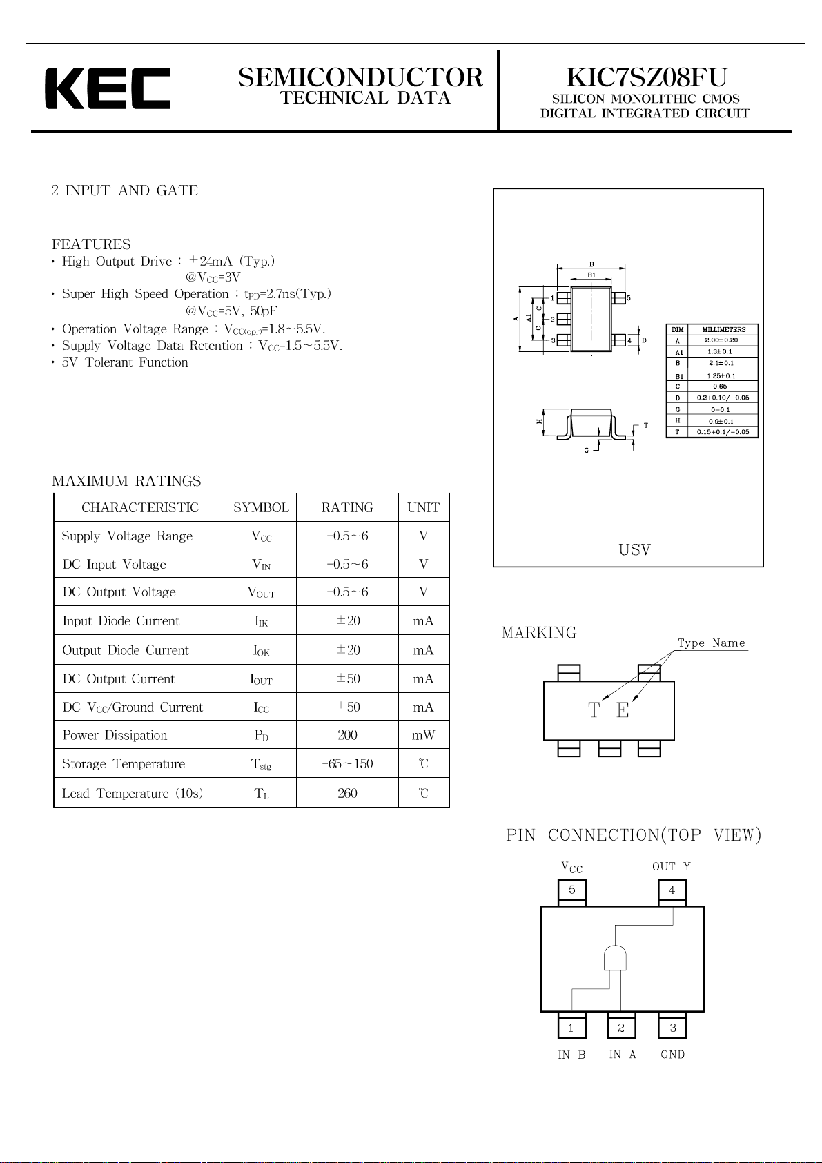
74LCX32
LOW VOLTAGE CMOS QUAD 2-INPUT OR GATE
WITH 5V TOLERANT INPUTS
■ 5V TOLERANT INPUTS
■ HIGH SPEED:
t
= 5.2ns (MAX.) at VCC = 3V
PD
■ POWER DOWN PROTECTION ON INPUTS
AND OUTPUTS
■ SYMMETRICAL OUTPUT IMPEDANCE:
|I
| = IOL = 24mA (MIN) at VCC = 3V
OH
■ PCI BUS LEVELS GUARANTEED AT 24 mA
■ BALANCED PROPAGATION DELAYS:
t
≅ t
PLH
■ OPERATING VOLTAGE RANGE:
V
CC
PHL
(OPR) = 2.0V to 3.6V (1.5V Data
Retention)
■ PIN AND FUNCTION COMPATIBLE WITH
74 SERIES 32
■ LATCH-UP PERFORMANCE EXCEEDS
500mA (JESD 17)
■ ESD PERFORMANCE:
HBM > 2000V (MIL STD 883 method 3015);
MM > 200V
DESCRIPTION
The 74LCX32 is a low voltage CMOS QUAD
2-INPUT OR GATE fabricated with sub-micron
silicon gate and double-layer metal wiring C
2
MOS
TSSOPSOP
Table 1: Order Codes
PACKAGE T & R
SOP 74LCX32MTR
TSSOP 74LCX32TTR
technology. It is ideal for low power and high
speed 3.3V applications; it can be interfaced to 5V
signal environment for inputs.
It has same speed performance at 3.3V than 5V
AC/ACT family, combined with a lower power
consumption.
All inputs and outputs are equipped with
protection circuits against static discharge, giving
them 2KV ESD immunity and transient excess
voltage.
Figure 1: Pin Connection And IEC Logic Symbols
Rev. 6
1/11September 2004
Page 52

181
AVR354 harman/kardon
74LCX32
Figure 2: Input And Output Equivalent Circuit
Table 2: Pin Description Table 3: Truth Table
PIN N° SYMBOL NAME AND FUNCTION
1, 4, 9, 12 1A to 4A Data Inputs
2, 5, 10, 13 1B to 4B Data Inputs
3, 6, 8, 11 1Y to 4Y Data Outputs
7 GND Ground (0V)
14
V
CC
Positive Supply Voltage
ABY
LLL
LHH
HLH
HHH
Table 4: Absolute Maximum Ratings
Symbol Parameter Value Unit
V
V
V
V
I
I
OK
I
I
CC
I
GND
T
T
Absolute Maximum Ratings are those values beyond which damage to the device may occur. Functional operation under these conditions is
not implied
1) IO absolute maximum rating must be observed
2) VO < GND
Supply Voltage
CC
DC Input Voltage
I
DC Output Voltage (VCC = 0V)
O
DC Output Voltage (High or Low State) (note 1) -0.5 to VCC + 0.5
O
DC Input Diode Current
IK
DC Output Diode Current (note 2)
DC Output Current
O
DC Supply Current per Supply Pin
DC Ground Current per Supply Pin
Storage Temperature
stg
Lead Temperature (10 sec)
L
-0.5 to +7.0 V
-0.5 to +7.0 V
-0.5 to +7.0 V
V
- 50 mA
- 50 mA
± 50 mA
± 100 mA
± 100 mA
-65 to +150 °C
300 °C
Page 53

182
AVR354 harman/kardon
74ACT04
HEX INVERTER
■ HIGH SPEED: t
■ LOW POWER DISSIPATION:
I
= 2µA(MAX.) at TA=25°C
CC
■ COMPAT I B L E WITH TTL OUTPUTS
V
= 2V (MIN.), VIL = 0.8V (MAX.)
IH
■ 50Ω TRANSMISSI O N L INE DRIVING
= 5.0ns (TYP.) at VCC = 5V
PD
CAPABILITY
■ SYMMETRICAL OUTPUT IMPEDANCE:
|I
| = IOL = 24mA (MIN)
OH
■ BALANCED PROPAGATION DELAYS:
t
≅ t
PLH
■ OPERA TING VOLTAGE RANGE:
V
CC
■ PIN AND FUNCTION COMPAT IBLE WITH
PHL
(OPR) = 4.5V to 5.5V
74 SERIES 04
■ IMPROVED LATCH-UP IMMUNITY
DESCRIPTION
The 74ACT04 is an advanced high-speed CMOS
HEX INVERTER fabricated with sub-micron
silicon gate and double-layer met al wiring C
2
MOS
technology.
The internal circuit is composed of 3 stages
including buffer output , which enables high noise
immunity and stable output.
TSSOPDIP SOP
ORDER CODES
PACKAGE TUBE T & R
DIP 74ACT04B
SOP 74ACT04M 74ACT04MTR
TSSOP 74ACT04TTR
The device is designed to interface directly High
Speed CMOS systems with TTL, NMOS and
CMOS output voltage levels.
All inputs and outputs are equipped with
protection circuits against stat ic discharge, giving
them 2KV ESD immunity and transient excess
voltage.
PIN CONNECTION AND IEC LOGIC SYMBOLS
1/8July 2001
Page 54

183
AVR354 harman/kardon
74ACT04
INPUT AND OUTPUT EQUIVALENT CIRCUIT PIN DESCRIPTION
PIN No SYMBOL NAME AND FUNCTION
1, 3, 5, 9, 1 1,
13
2, 4, 6, 8, 10,
12
7 GND Ground (0V)
14
TRUTH TABLE
ABSOLUTE MAXIMUM RATINGS
1A to 6A Data Inputs
1Y to 6Y Data Outputs
V
CC
Positive Supply Voltage
AY
LH
HL
Symbol Parameter Value Unit
V
V
V
I
I
OK
I
I
or I
CC
T
T
Absolute Maximum Ratings are those values beyond which damage to the device may occur. Functional operation under these conditions is
not implied.
Supply Voltage
CC
DC Input Voltage -0.5 to VCC + 0.5
I
DC Output Voltage -0.5 to VCC + 0.5
O
DC Input Diode Current
IK
DC Output Diode Current
DC Output Current
O
DC VCC or Ground Current
GND
Storage Temperature
stg
Lead Temperature (10 sec)
L
-0.5 to +7 V
V
V
± 20 mA
± 20 mA
± 50 mA
± 200 mA
-65 to +150 °C
300 °C
RECOMMENDED OPERATING CONDITIONS
Symbol Parameter Value Unit
V
V
V
T
dt/dv
1) VIN from 0.8V to 2.0V
Supply Voltage
CC
Input Voltage 0 to V
I
Output Voltage 0 to V
O
Operating Temperature
op
Input Rise and Fall Time V
= 4.5 to 5.5V (note 1)
CC
4.5 to 5.5 V
CC
CC
-55 to 125 °C
8 ns/V
V
V
2/8
Page 55

184
AVR354 harman/kardon
CS42528
114 dB, 192 kHz 8-Ch Codec with S/PDIF Receiver
Features
z Eight 24-bit D/A, two 24-bit A/D Converters
z 114 dB DAC / 114 dB ADC Dynamic Range
z -100 dB THD+N
z System Sampling Rates up to 192 kHz
z S/PDIF Receiver Compatible with EIAJ CP1201
and IEC-60958
z Recovered S/PDIF Clock or System Clock
Selection
z 8:2 S/PDIF Input MUX
z ADC High-pass Filter for DC Offset Calibration
z Expandable ADC Channels and One-line Mode
Support
z Digital Output Volume Control with Soft Ramp
z Digital +/-15dB Input Gain Adjust for ADC
z Differential Analog Architecture
z Supports logic levels between 5 V and 1.8 V.
RXP0
RXP1/GPO1
RXP2/GPO2
RXP3/GPO3
RXP4/GPO4
RXP5/GPO5
RXP6/GPO6
RXP7/GPO7
MUTEC
FILT+
REFGND
AGND
AINL+
AINL-
AINR+
AINR-
AOUTA1+
AOUTA1-
AOUTB1+
AOUTB1-
AOUTA2+
AOUTA2-
AOUTB2+
AOUTB2-
AOUTA3+
AOUTA3-
AOUTB3+
AOUTB3-
AOUTA4+
AOUTA4-
AOUTB4+
AOUTB4-
VARX AGND
TXP
Rx
GPO
MUTE
VQ
VA
Ref
ADC#1
ADC#2
r
e
t
l
i
F
g
o
l
a
n
A
Clock/Data
Recovery
Digita l Filter
Digita l Filter
LPFLT
DAC#1
DAC#2
DAC#3
DAC#4
DAC#5
DAC#6
DAC#7
DAC#8
General Description
The CS42528 codec provides two analog-to-digital and eight
digital-to-analog delta-sigma converters, as well as an integrated S/PDIF receiver, in a 64-pin LQFP package.
The CS42528 integrated S/PDIF receiver supports up to eight
inputs, clock recovery circuitry and format auto-detection. The
internal stereo ADC is capable of independent channel gain
control for single-ended or differential analog inputs. All eight
channels of DAC provide digital volume control and differential
analog outputs. The general purpose outputs may be driven
high or low, or mapped to a variety of DAC mute controls or
ADC overflow indicators.
The CS42528 is ideal for audio systems requiring wide dynamic range, negligible distortion and low noise, such as A/V
receivers, DVD receivers, digital speaker and automotive audio
systems.
ORDERING INFORMATION
CS42528-CQZ -10° to 70° C 64-pin LQFP Lead Free
CS42528-DQZ -40° to 85° C 64-pin LQFP Lead Free
CDB42528 Evaluation Board
DGND
S/PDIF
Decoder
DEM
Gain & Clip
Gain & Clip
r
e
t
l
i
F
l
a
t
i
g
i
D
DGND
C&U Bit
Data Bu ffer
Format
Detector
ADC
Serial
Data
Internal M CLK
VD
VD
INT
Control
Port
Mult/Div
Serial
Audio
Interfa ce
Port
CODEC
l
o
r
Serial
t
n
o
C
me
u
l
o
V
Port
RST
AD0/CS
AD1/CDIN
SDA/CDOUT
SCL/CCLK
VLC
OMCK
RMCK
SAI_LRCK
SAI_SCLK
SAI_SDOUT
VLS
ADCIN1
ADCIN2
CX_SDOUT
CX_LRCK
CX_SCLK
CX_SDIN1
CX_SDIN2
CX_SDIN3
CX_SDIN4
Preliminary Product Information
Cirrus Logic, Inc.
http://www.cirrus.com
Page 56
185
AVR354 harman/kardon
CS42528
2. PIN DESCRIPTIONS
CX_SDIN2
CX_SDIN4
CX_SDIN3
64 63 62 61 60 59 58 57 56 55 54 53 52 51 50 49
CX_SDIN1
CX_SCLK
CX_LRCK
SCL/CCLK
SDA/CDOUT
AD1/CDIN
AD0/CS
VD
DGND
VLC
INT
RST
AINR-
AINR+
AINL+
AINL-
1
2
3
4
5
6
7
8
9
10
11
12
13
14
15
16
17 18 19 20 21 22 23 24 25 26 27 28 29 30 31 32
ADCIN2
ADCIN1
OMCK
SAI_SCLK
SAI_LRCK
CS42528
CX_SDOUT
RMCK
T
VLS
SAI_SDOU
DGND
VD
TXP
RXP0
48
47
46
45
44
43
42
41
40
39
38
37
36
35
34
33
RXP1/GPO1
RXP2/GPO2
RXP3/GPO3
RXP4/GPO4
RXP5/GPO5
RXP6/GPO6
RXP7/GPO7
VARX
AGND
LPFLT
MUTEC
AOUTA1-
AOUTA1+
AOUTB1+
AOUTB1-
AOUTA2-
VQ
FILT+
REFGND
AOUTB4-
AOUTB4+
VA
AGND
AOUTA4-
AOUTA4+
AOUTB3-
AOUTB3+
AOUTB2-
AOUTA3-
AOUTB2+
AOUTA3+
AOUTA2+
Pin Name # Pin Description
CX_SDIN1
CX_SDIN2
CX_SDIN3
CX_SDIN4
CX_SCLK 2 CODEC Serial Clock (Input/Output) - Serial clock for the CODEC serial audio interface.
CX_LRCK 3 CODEC Left Right Clock (Input/Output) - Determines which channel, Left or Right, is currently active on
VD 451Digital Power (Input) - Positive power supply for the digital section.
DGND 552Digital Ground (Input) - Ground reference. Should be connected to digital ground.
VLC 6
SCL/CCLK 7 Serial Control Port Clock (Input) - Serial clock for the serial control port. Requires an external pull-up
SDA/CDOUT 8 Serial Control Data (Input/Output) - SDA is a data I/O line in I
AD1/CDIN 9 Address Bit 1 (I2C)/Serial Control Data (SPI) (Input) - AD1 is a chip address pin in I
1
Codec Serial Audio Data Input (Input) - Input for two’s complement serial audio data.
64
63
62
the CODEC serial audio data line.
Control Port Power (Input) - Determines the required signal level for the control port.
resistor to the logic interface voltage in I
2
C mode as shown in the Typical Connection Diagram.
2
C mode and requires an external pull-up
resistor to the logic interface voltage, as shown in the Typical Connection Diagram. CDOUT is the output
data line for the control port interface in SPI mode.
2
C mode; CDIN is
the input data line for the control port interface in SPI mode.
Page 57

186
AVR354 harman/kardon
CS42528
AD0/CS 10
INT 11 Interrupt (Output) - The CS42528 will generate an interrupt condition as per the Interrupt Mask register.
RST 12 Reset (Input) - The device enters a low power mode and all internal registers are reset to their default
AINRAINR+
AINL+
AINL-
VQ 17 Quiescent Voltage (Output) - Filter connection for internal quiescent reference voltage.
FILT+ 18 Positive Voltage Reference (Output) - Positive reference voltage for the internal sampling circuits.
REFGND 19 Reference Ground (Input) - Ground reference for the internal sampling circuits.
AOUTA1 +,AOUTB1 +,AOUTA2 +,AOUTB2 +,AOUTA3 +,AOUTB3 +,AOUTA4 +,AOUTB4 +,-
VA
VARX
AGND 2540Analog Ground (Input) - Ground reference. Should be connected to analog ground.
Address Bit 0 (I
is the chip select signal in SPI mode.
See “Interrupts” on page 40 for more details.
settings when low.
13
Differential Right Channel Analog Input (Input) - Signals are presented differentially to the delta-sigma
14
modulators via the AINR+/- pins.
15
Differential Left Channel Analog Input (Input) - Signals are presented differentially to the delta-sigma
16
modulators via the AINL+/- pins.
36,37
Differential Analog Output (Output) - The full-scale differential analog output level is specified in the
35,34
Analog Characteristics specification table.
32,33
31,30
28,29
27,26
22,23
21,20
24
Analog Power (Input) - Positive power supply for the analog section.
41
2
C)/Control Port Chip Select (SPI) (Input) - AD0 is a chip address pin in I
2
C mode; CS
MUTEC 38 Mute Control (Output) - The Mute Control pin outputs high impedance following an initial power-on con-
dition or whenever the PDN bit is set to a ‘1’, forcing the codec into power-down mode. The signal will
remain in a high impedance state as long as the part is in power-down mode. The Mute Control pin goes
to the selected “active” state during reset, muting, or if the master clock to left/right clock frequency ratio
is incorrect. This pin is intended to be used as a control for external mute circuits to prevent the clicks
and pops that can occur in any single supply system. The use of external mute circuits are not manda-
tory but may be desired for designs requiring the absolute minimum in extraneous clicks and pops.
LPFLT 39 PLL Loop Filter (Output) - An RC network should be connected between this pin and ground.
RXP7/GPO7
RXP6/GPO6
RXP5/GPO5
RXP4/GPO4
RXP3/GPO3
RXP2/GPO2
RXP1/GPO1
RXP0 49 S/PDIF Receiver Input (Input) - Dedicated receiver input for S/PDIF encoded data.
TXP 50 S/PDIF Transmitter Output (Output) - S/PDIF encoded data output, mapped directly from one of the
VLS 53 Serial Port Interface Power (Input) - Determines the required signal level for the serial port interfaces.
SAI_SDOUT
RMCK 55 Recovered Master Clock (Output) - Recovered master clock output from the External Clock Reference
42
S/PDIF Receiver Input/ General Purpose Output (Input/Output) - Receiver inputs for S/PDIF encoded
43
data. The CS42528 has an internal 8:2 multiplexer to select the active receiver port, according to the
44
Receiver Mode Control 2 register. These pins can also be configured as general purpose output pins,
45
ADC Overflow indicators or Mute Control outputs according to the RXP/General Purpose Pin Control
46
registers.
47
48
receiver inputs as indicated by the Receiver Mode Control 2 register.
54 Serial Audio Interface Serial Data Output (Output) - Output for two’s complement serial audio PCM
data from the S/PDIF incoming stream. This pin can also be configured to transmit the output of the inter-
nal and external ADCs.
(OMCK, pin 59) or the PLL which is locked to the incoming S/PDIF stream or CX_LRCK.
Page 58

187
AVR354 harman/kardon
CS42528
CX_SDOUT 56 CODEC Serial Data Output (Output) - Output for two’s complement serial audio data from the internal
and external ADCs.
ADCIN1
ADCIN2
OMCK 59 External Reference Clock (Input) - External clock reference that must be within the ranges specified in
SAI_LRCK 60 Serial Audio Interface Left/Right Clock (Input/Output) - Determines which channel, Left or Right, is
SAI_SCLK 61 Serial Audio Interface Serial Clock (Input/Output) - Serial clock for the Serial Audio Interface.
58
External ADC Serial Input (Input) - The CS42528 provides for up to two external stereo analog to digital
57
converter inputs to provide a maximum of six channels on one serial data output line when the CS42528
is placed in One Line mode.
the register “OMCK Frequency (OMCK Freqx)” on page 54.
currently active on the serial audio data line.
Page 59

SEMICONDUCTOR
TECHNICAL DATA
KIA378R05PI~KIA378R15PI
BIPOLAR LINEAR INTEGRATED CIRCUIT
Revision No : 3
4 TERMINAL 3A OUTPUT LOW DROP
VOLTAGE REGULATOR
The KIA378R Series are Low Drop Voltage
Regulator suitable for various electronic equipments.
It provides constant voltage power source with TO-220IS-4
terminal lead full molded PKG.
The Regulator has multi-function such as over current
protection, overheat protection and ON/OFF control.
FEATURES
3.0A Output Low Drop Voltage Regulator.
Built in ON/OFF Control Terminal.
Built in Over Current Protection, Over Heat
Protection Function.
LINE UP
MAXIMUM RATINGS (Ta=25 )
ITEM OUTPUT VOLTAGE (Typ.) UNIT
KIA378R05PI 5
V
KIA378R06PI 6
KIA378R08PI 8
KIA378R09PI 9
KIA378R10PI 10
KIA378R12PI 12
KIA378R15PI 15
CHARACTERISTIC SYMBOL RATING UNIT Remark
Input Voltage
V
IN
35 V -
ON/OFF Control Voltage
V
C
35 V -
Output Current
I
O
3 A -
Power Dissipation 1
P
d1
1.5 W No heatsink
Power Dissipation 2
P
d2
15 W with heatsink
Junction Temperature
T
j
-40 150
-
Operating Temperature
T
opr
-30 85
-
Storage Temperature
T
stg
-40 150
-
Soldering Temperature (10sec)
T
sol
260 -
188
AVR354 harman/kardon
C
O
S
H
DIM
A
B
C
D
E
F
G
H
J
R
K
L
M
N
O
P
R
S
T
U
V
DC INPUT (V )
1
DC OUTPUT (V )
2
GND
3
ON/OFF CONTROL
4
MILLIMETERS
_
+
10.00 0.20
_
+
15.00 0.20
_
+
2.70 0.20
_
+
0.60 0.10
_
+
Φ3.20 0.20
_
+
3.50 0.10
_
+
15.70 0.20
_
+
0.40 0.10
14.3+0.2/-0.1
_
+
1.45 0.10
_
+
1.00 0.10
2.54
_
+
4.50 0.20
_
+
7.5 0.1
_
+
1.50 0.10
5
8
_
+
1.30 0.1
_
+
3-1.00 0.1
_
+
1.30 0.1
IN
O
E
B
L
J
P
A
V
V
T
M
1234
F
G
L
K
U
D
N
TO-220IS-4
Page 60
SEMICONDUCTOR
TECHNICAL DATA
KIA278R00PI
BIPOLAR LINEAR INTEGRATED CIRCUIT
2A ADJUSTABLE LOW DROP VOLTAGE REGULATOR
The KIA278R00PI is a Low Drop Voltage Regulator suitable
for various electronic equipments. It provides constant voltage
power source with TO-220-4 terminal lead full molded PKG.
The Regulator has multi function such as over current protection,
overheat protection.
FEATURES
Adjustable Output Voltage (Range : 1.5~30V)
1.0A Output Low Drop Voltage Regulator.
Built in Over Current Protection, Over Heat Protection Function.
MAXIMUM RATINGS (Ta=25 )
CHARACTERISTIC SYMBOL RATING UNIT Remark
Input Voltage
V
IN
35 V -
Output Current
I
OUT
2 A -
Power Dissipation 1
P
D1
1.5 W No heatsink
Power Dissipation 2
P
D2
15 W with heatsink
Junction Temperature
T
j
150 -
Operating Temperature
T
opr
-20 80
-
Storage Temperature
T
stg
-30 150
-
Soldering Temperature (10sec)
T
sol
260 -
189
AVR354 harman/kardon
C
DIM MILLIMETERS
A
B
O
S
H
C
D
E
F
G 15.70 0.20
J
R
K
L
M
N
O
P
R
S
T
U
V
1
2
3
4
_
+
10.00 0.20
_
+
15.00 0.20
_
+
2.70 0.20
_
+
0.60 0.10
_
+
Φ3.20 0.20
_
+
3.50 0.10
_
+
_
+
0.40 0.10H
14.3+0.2/-0.1
_
+
1.45 0.10
_
+
1.00 0.10
2.54
_
+
4.50 0.20
_
+
7.5 0.1
_
+
1.50 0.10
5
8
_
+
1.30 0.1
_
+
3-1.00 0.1
_
+
1.30 0.1
DC INPUT (V )
DC OUTPUT (V )
GND
ADJUSTABLE
TERMINAL
(V )
IN
ADJ
E
B
L
U
J
P
1234
A
F
G
V
V
L
K
T
D
M
N
O
TO-220IS-4
Page 61

190
AVR354 harman/kardon
SEMICONDUCTOR
TECHNICAL DATA
4 TERMINAL 2A OUTPUT LOW DROP
VOLTAGE REGULATOR
The KIA278Rᴧᴧ Series are Low Drop Voltage Regulator
suitable for various electronic equipments.
It provides constant voltage power source with TO-220 4 terminal
lead full molded PKG. The Regulator has multi function such as
over current protection, overheat protection and ON/OFF control.
FEATURES
ᴌ2.0A Output Low Drop Voltage Regulator.
ᴌBuilt in ON/OFF Control Terminal.
ᴌBuilt in Over Current Protection, Over Heat
Protection Function.
LINE UP
ITEM OUTPUT VOLTAGE (Typ.) UNIT
KIA278R05PI 5
KIA278R05PI~KIA278R15PI
BIPOLAR LINEAR INTEGRATED CIRCUIT
C
O
S
H
DIM
A
B
C
D
E
F
G
H
J
R
K
L
M
N
O
P
R
S
T
U
V
DC INPUT (V )
1
DC OUTPUT (V )
2
GND
3
ON/OFF CONTROL
4
MILLIMETERS
_
+
10.00 0.20
_
+
15.00 0.20
_
+
2.70 0.20
_
+
0.60 0.10
_
+
Φ3.20 0.20
_
+
3.50 0.10
_
+
15.70 0.20
_
+
0.40 0.10
14.3+0.2/-0.1
_
+
1.45 0.10
_
+
1.00 0.10
2.54
_
+
4.50 0.20
_
+
7.5 0.1
_
+
1.50 0.10
5
8
_
+
1.30 0.1
_
+
3-1.00 0.1
_
+
1.30 0.1
IN
O
E
B
L
J
P
A
V
V
T
M
1234
F
G
L
K
U
D
N
TO-220IS-4
KIA278R06PI 6
KIA278R08PI 8
KIA278R09PI 9
KIA278R10PI 10
KIA278R12PI 12
* KIA278R15PI 15
* Note) * : Under Development.
MAXIMUM RATING (Ta=25ᴱ)
CHARACTERISTIC SYMBOL RATING UNIT Remark
Input Voltage
ON/OFF Control Voltage
Output Current
Power Dissipation 1
Power Dissipation 2
Junction Temperature
Operating Temperature
Storage Temperature
Soldering Temperature (10sec)
V
V
IN
V
C
I
O
P
d1
P
d2
T
j
T
opr
T
stg
T
sol
35 V -
35 V -
2 A -
1.5 W No heatsink
15 W with heatsink
125
-20ᴕ80
-30ᴕ125
260
ᴱ
ᴱ
ᴱ
ᴱ
-
-
-
-
Page 62

2005. 3. 14 1/7
SEMICONDUCTOR
TECHNICAL DATA
KIA1117S/F00~
KIA1117S/F50
BIPOLAR LINEAR INTEGRATED CIRCUIT
Revision No : 0
LOW DROP FIXED AND ADJUSTABLE
POSITIVE VOLTAGE REGULATOR
The KIA1117S/F is a Low Drop Voltage Regulator able
to provide up to 1A of output current, available even in adjustable
version (Vref=1.25V)
FEATURES
Low Dropout Voltage : 1.1V/Typ. (Iout=1.0A)
Very Low Quiescent Current : 4.2 /Typ.
Output Current up to 1A
Fixed Output Voltage of 1.5V, 1.8V, 2.5V, 2.85V, 3.3V, 5.0V
Adjustable Version Availability : Vref=1.25V
Internal Current and Thermal Limit
Only 10 for stability
Available in 2%(at 25 ) and 4% in full Temperature range
High Ripple Rejection : 80dB/Typ
Temperature Range : 0 125
LINE UP
ITEM OUTPUT VOLTAGE (V) PACKAGE
KIA1117S/F00 Adjustable (1.25~10V)
S : SOT-223
F : DPAK
KIA1117S/F15 1.5
KIA1117S/F18 1.8
KIA1117S/F25 2.5
KIA1117S/F28 2.85
KIA1117S/F33 3.3
KIA1117S/F50 5.0
MAXIMUM RATINGS (Ta=25 )
CHARACTERISTIC SYMBOL RATING UNIT
Input Voltage
V
IN
10 V
Output Current S/F
I
OUT
1.0 A
Power Dissipation 1
(No heatsink)
S (Note)
P
D1
1.0
W
F 1.3
Power Dissipation 2
(Without heatsink)
S
P
D2
8.3
W
F 13
Operating Temperature
T
opr
0 125
Storage Temperature
T
stg
-55 150
Note) Package Mounted on FR-4 PCB 36 18 1.5 .
: mounting pad for the GND Lead min. 6
191
AVR354 harman/kardon
A
B
E
J
C
1. COMMOIN (ADJ.)
2. OUTPUT
3. INPUT
H
F
F
1
3
2
D
SOT-223
L
K
G
DIM MILLIMETERS
A
B
C
D
E
F
G
H
J
K
L
_
6.5 0.2
+
_
3.5 0.2
+
1.8 MAX
0.7+0.15/-0.1
_
+
7 0.3
2.3 TYP
0.26+0.09/-0.02
3.0+0.15/-0.1
_
1.75 0.25
+
0.1 MAX
10 MAX
A
C
Q
H
F
123
1. COMMOIN (ADJ.)
2. OUTPUT
3. INPUT
I
J
D
B
M
K
E
P
F
DIM MILLIMETERS
A
B
C
D
E
F
H
I
O
J
K
L
L
_
+
6.60 0.2
_
+
6.10 0.2
_
5.0 0.2
+
_
1.10 0.2
+
_
+
2.70 0.2
_
+
2.30 0.1
1.00 MAX
_
+
2.30 0.2
_
+
0.5 0.1
_
+
2.00 0.20
_
+
0.50 0.10
_
+
0.91 0.10M
_
+
0.90 0.1O
_
+
1.00 0.10P
0.95 MAXQ
DPAK
Page 63

192
AVR354 harman/kardon
RE5VT28C ATZ
PIN CONFIGURATION
•
TO-92
•
SOT-89
•
SOT-23-5
5
4
(mark side)
12
3
PIN DESCRIPTION
•
TO-92
Pin No. Symbol
1 OUT
2VDD
(mark side)
12
•
SOT-89
Pin No. Symbol
1 OUT
2VDD
3
(mark side)
12
Pin No. Symbol
3
•
SOT-23-5
1 OUT
2VDD
3 GND
BLOCK DIAGRAMS
• Nch Open Drain Output (R
V
DD
2
Vref
×
5VT××A) • CMOS Output (R×5VT××C)
+
–
TIME CHART
1
3
OUT
GND
3 GND
VDD
2
Vref
3 GND
4NC
5NC
+
–
OUT
1
3
GND
Page 64

193
AVR354 harman/kardon
TRANSISTOR, REGULATOR IC BLOCK DIAGRAM
TO-92M
1. Emitter
2. Collector
3. Base
123
KTC2874B
KRA107M
KRA104MT
KTA1267
KSC2785Y
KRC107M
KRC104M
TO-126
1. Emitter
2. Collector
3. Base
123
2
KTD600KG
2
TO-92
123
KTD1302T
KTC3200GR
KTA1271Y
TO-92
123
KSA733CYT
1. Emitter
2. Collector
3. Base
KTA1268GR
KTC3198Y
KSA1175YT
1. Emitter
2. Base
3. Collector
TO-220
1. GND
2. INPUT
3. OUTPUT
123
MCNJM7905 MC7915C
NJM7908
L7905
L7915
TO-220
1. INPUT
2. GND
3. OUTPUT
123
MC7815C MC7805C
MC7809
NJM7824
L7805
L7815
L7812
L7808
TO-92L
1. Emitter
2. Collector
3. Base
123
KTA1024Y KSC2316Y
TO-3P
1. Base
2. Collector
3. Emitter
123
2SB1560
2SD2390
2SA1360
2SB1647
2SD2560
2SC3423O
N-CHANNEL MOS FET ARRAY
µPA672T
654
Source 1
1.
Gate 1
2.
Drain 2
3.
Source 2
4.
Gate 2
5.
Drain 1
6.
123
Marking: MA
(S1)
(G1)
(D2)
(S2)
(G2)
(D1)
PIN CONFIGURATION
SOT-23 Package
AD1580
1
V+
NC (OR V–)
3
2
V–
TOP
VIEW
NC = NO CONNECT
KRA107S
SOT-223 PKG (FRONT VIEW)
LM1117
REGULATOR
PIN FUNCTION
1. Adj/Gnd
2. Vout
1 2 3
TO-263 (D2 PKG, FRONT VIEW)
3. Vin
PIN FUNCTION
1. Adj/Gnd
2. Vout
3. Vin
1 2 3
Page 65

194
AVR354 harman/kardon
Page 66

195
AVR354 harman/kardon
Page 67

196
AVR354 harman/kardon
Page 68

197
AVR354 harman/kardon
Page 69

198
AVR354 harman/kardon
Page 70

199
AVR354 harman/kardon
Page 71

200
AVR354 harman/kardon
Page 72

AVRx54Front_0119.sch-1-FriFeb0815:10:472008
201
AVR354 harman/kardon
Page 73

202
AVR354 harman/kardon
AVR355input_0208.sch-1-FriFeb0815:54:262008
Page 74

203
AVR354 harman/kardon
AVR355input_0208.sch-2-FriFeb0815:54:522008
Page 75

204
AVR354 harman/kardon
AVR355input_0208.sch-3-FriFeb0815:55:292008
Page 76

080121 AVR355 VIDEO sample.sch-1 - Sat Feb 02 16:43:21 2008
205
AVR354 harman/kardon
VID3
Page 77

080121 AVR355 VIDEO sample.sch-2 - Sat Feb 02 16:43:48 2008
206
AVR354 harman/kardon
Page 78

207
AVR354 harman/kardon
Page 79

AVR354 WIRING.sch-1 - Wed Apr 23 11:54:01 2008
208
AVR354 harman/kardon
 Loading...