

Page 1
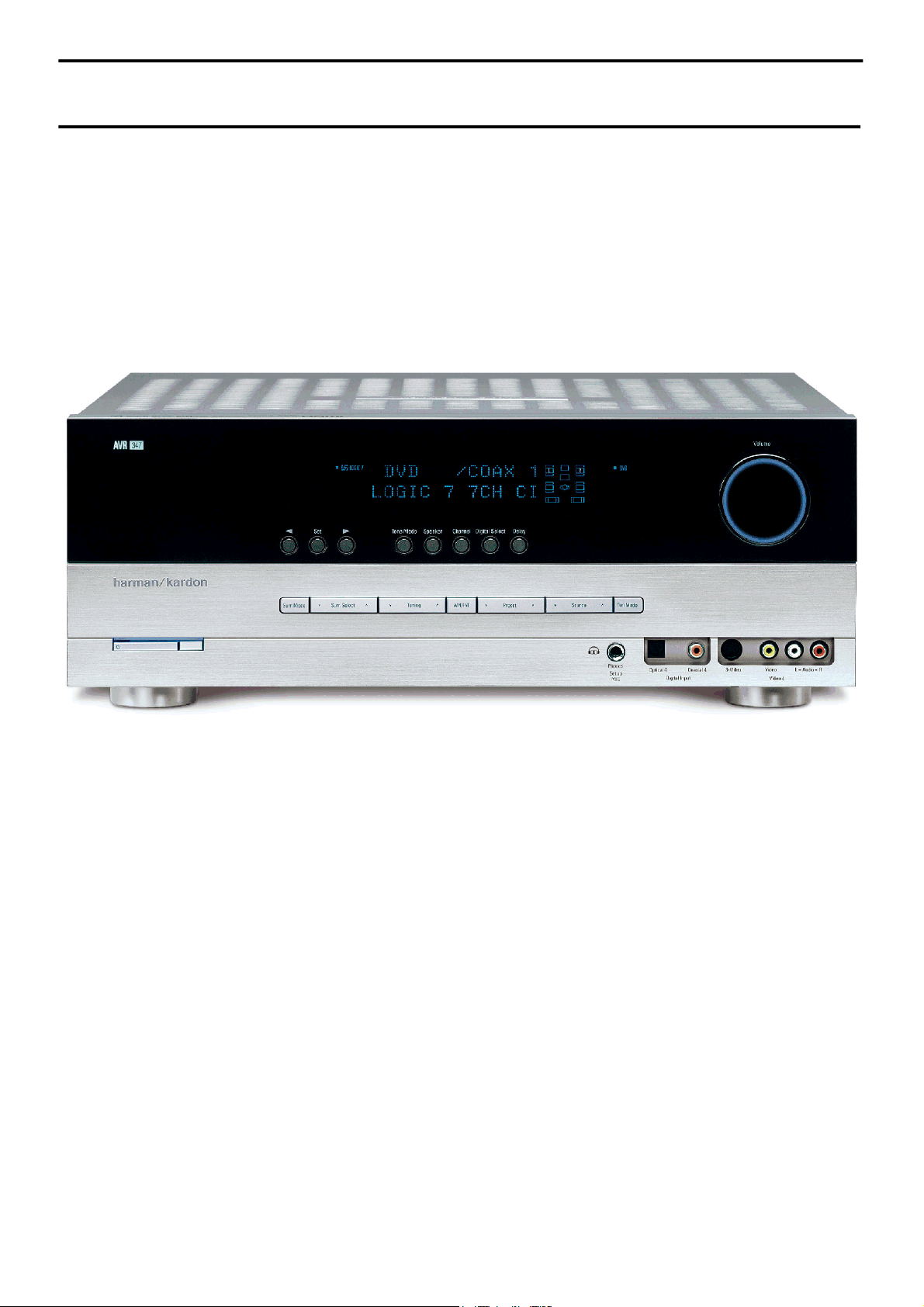
harman/kardon
AVR 347/230, AVR 350/230 Semiconductor Pinouts
Page 1 of 51
harman/kardon Service Manual
AVR 347/230
AVR 350/230
7 x 55W 7.1 CHANNEL A/V RECEIVERS
THIS MANUAL CONTAINS SEMICONDUCTOR PINOUTS ONLY.
Main Service Manual in separate file
CONTENTS
Released EU2008 harman/kardon, Inc. Rev 0, 07/2008
250 Crossways Park Dr.
Woodbury, New York, 11797
Page 2
54
∗hFE Rank O(5000to12000), P(6500to20000), Y(15000to30000)
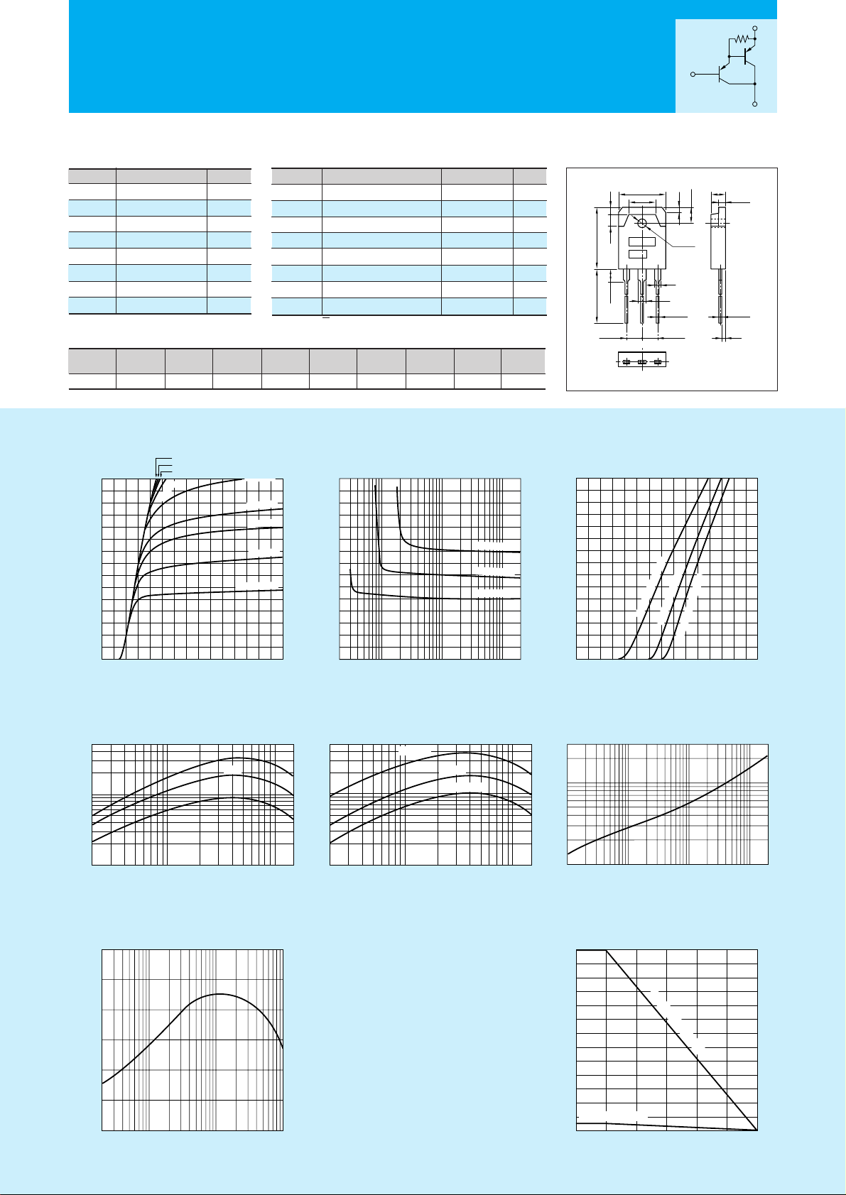
Darlington 2SB1647
IC
–
V
CE Characteristics
(Typical)
hFE
–
I
C Characteristics
(Typical)
hFE
–
I
C
Temperature Characteristics (Typical)
IC
–
V
BE Temperature Characteristics
(Typical)
VCE(sat)–IB Characteristics
(Typical)
Pc–Ta Derating
–10mA
–50mA
–3mA
0
–3
–2
–1
–0.2
–1–0.5 –10–5 –200–100–50
Base Current IB(mA)
Collector-Emitter Saturation Voltage VCE(sat)(V)
I
C
=–10A
I
C
=–15A
IC =–5A
0
–15
–10
–5
0–3–2–1
Base-Emittor Voltage V
BE(V)
Collector Current IC(A)
(VCE=–4V)
125˚C (Case Temp)
25˚C (Case Temp)
–30˚C (Case Temp)
–0.2 –0.5 –1 –5 –10 –15
Collector Current I
C(A)
DC Current Gain hFE
(VCE=–4V)
1,000
10,000
50,000
5,000
Typ
(VCE=–4V)
–0.2 –1–0.5 –5 –10 –15
1000
5000
10000
50000
Collector Current IC(A)
DC Current Gain hFE
25˚C
–30˚C
125˚C
Time t(ms)
0.1
1
3
0.5
1 10 100 1000 2000
Transient Thermal Resistance θj-a(˚C/W)
0.02 0.10.05 0.5 1 5 10
0
40
20
60
Cut-off Frequency fT(MHZ)
(VCE=–12V)
Emitter Current I
E(A)
Safe Operating Area (Single Pulse)
θj-a
–
t
Characteristics
f
T
–
I
E Characteristics
(Typical)
0
0
–5
–10
–15
–2 –6–4
Collector-Emitter Voltage VCE(V)
Collector Current IC(A)
–1.5mA
–1.0mA
–0.8mA
I
B
=–0.3mA
–0.5mA
–2mA
130
100
50
3.5
0
Ambient Temperature Ta(˚C)
Maximum Power Dissipation PC(W)
With Infinite heatsink
Without Heatsink
0 25 50 75 100 125 150
Silicon PNP Epitaxial Planar Transistor (Complement to type 2SD2560)
Application : Audio, Series Regulator and General Purpose
Symbol
V
CBO
VCEO
VEBO
IC
IB
PC
Tj
T
stg
2SB1647
–150
–150
–5
–15
–1
130(Tc=25°C)
150
–55 to +150
Unit
V
V
V
A
A
W
°C
°C
■
Absolute maximum ratings
■
Electrical Characteristics
Symbol
I
CBO
IEBO
V(BR)CEO
hFE
VCE(sat)
VBE(sat)
fT
COB
2SB1647
–100
max
–100max
–150min
5000min∗
–2.5
max
–3.0max
45typ
320typ
Unit
µ
A
µ
A
V
V
V
MHz
pF
Conditions
V
CB=–150V
V
EB=–5V
I
C=–30mA
V
CE=–4V, IC=–10A
I
C=–10A, IB=–10mA
I
C=–10A, IB=–10mA
V
CE=–12V, IE=2A
V
CB=–10V, f=1MHz
(Ta=25°C) (Ta=25°C)
External Dimensions MT-100(TO3P)
15.6
±0.4
9.6
19.9
±0.3
4.0 2.0
5.0
±0.2
1.8
ø3.2
±0.1
2
3
1.05
+0.2
-0.1
20.0min
4.0max
BE
5.45
±0.1
5.45
±0.1
C
4.8
±0.2
0.65
+0.2
-0.1
1.4
2.0
±0.1
a
b
■Typical Switching Characteristics (Common Emitter)
V
CC
(V)
–40
RL
(Ω)
4
I
C
(A)
10
V
BB2
(V)
5
I
B2
(mA)
10
t
on
(µs)
0.7typ
t
stg
(µs)
1.6typ
t
f
(µs)
1.1typ
IB1
(mA)
–10
VBB1
(V)
–10
Weight : Approx 6.0g
a. Type No.
b. Lot No.
E
Equivalent circuit
harman/kardon
AVR 347/230, AVR 350/230 Semiconductor Pinouts
Page 2 of 51
(70Ω)
B
C
Page 3
158
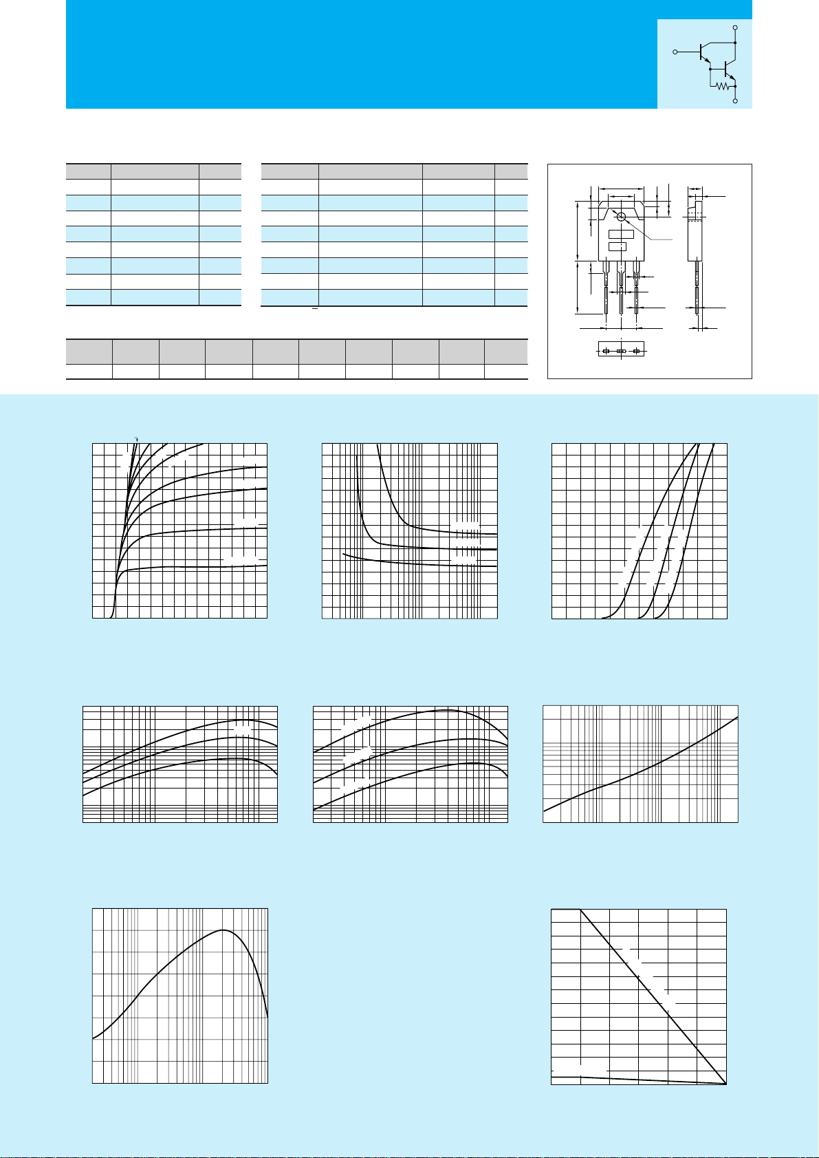
Silicon NPN Triple Diffused Planar Transistor (Complement to type 2SB1647)
Application : Audio, Series Regulator and General Purpose
Symbol
V
CBO
VCEO
VEBO
IC
IB
PC
Tj
T
stg
2SD2560
150
150
5
15
1
130(Tc=25°C)
150
–55to+150
Unit
V
V
V
A
A
W
°C
°C
■
Absolute maximum ratings
■
Electrical Characteristics
Symbol
I
CBO
IEBO
V(BR)CEO
hFE
VCE(sat)
VBE(sat)
fT
COB
2SD2560
100
max
100max
150min
5000min∗
2.5
max
3.0max
70typ
120typ
Unit
µ
A
µ
A
V
V
V
MHz
pF
Conditions
V
CB=150V
V
EB=5V
I
C=30mA
V
CE=4V, IC=10A
I
C=10A, IB=10mA
I
C=10A, IB=10mA
V
CE=12V, IE=–2A
V
CB=10V, f=1MHz
Darlington 2SD2560
(Ta=25°C) (Ta=25°C)
IC
–
V
CE Characteristics
(Typical)
Safe Operating Area (Single Pulse)
0
0
10
5
15
246
Collector-Emitter Voltage V
CE(V)
Collector Current IC(A)
50mA
I
B
=0.3mA
0.5mA
0.8mA
2mA
1.0mA
3mA
10mA
1.5mA
VCE(sat)–IB Characteristics
(Typical)
0
3
2
1
0.2
10.5 105 20010050
Base Current IB(mA)
Collector-Emitter Saturation Voltage VCE(sat)(V)
IC =.15A
IC =.10A
IC =.5A
IC
–
V
BE Temperature Characteristics
(Typical)
0
15
5
10
0 2 2.21
Base-Emittor Voltage V
BE(V)
Collector Current IC(A)
(VCE=4V)
125˚C (Case Temp)
25˚C (Case Temp)
–30˚C (Case Temp)
hFE
–
I
C Characteristics
(Typical)
Collector Current IC(A)
02 0.5 1 10 155
50000
1000
5000
10000
500
DC Current Gain hFE
(VCE=4V)
Typ
02 0.5 1 10 155
50000
1000
5000
10000
500
DC Current Gain hFE
(VCE=4V)
hFE
–
I
C
Temperature Characteristics (Typical)
Collector Current IC(A)
125˚C
–30˚C
25˚C
θj-a
–
t
Characteristics
0.1
1.0
3.0
0.5
1 10 100 1000 2000
Time t(ms)
Transient Thermal Resistance θj-a(˚C/W)
fT
–
I
E Characteristics
(Typical)
(VCE=12V)
Emitter Current I
E(A)
–0.05–0.02 –01 –0.5 –1 –5 –10
0
40
20
60
80
Cut-off Frequency fT(MHZ)
Pc–Ta Derating
130
100
50
3.5
0
Ambient Temperature Ta(˚C)
Maximum Power Dissipation PC(W)
With Infinite heatsink
Without Heatsink
0 25 50 75 100 125 150
External Dimensions MT-100(TO3P)
15.6
±0.4
9.6
19.9
±0.3
4.0 2.0
5.0
±0.2
1.8
ø3.2
±0.1
2
3
1.05
+0.2
-0.1
20.0min
4.0max
BE
5.45
±0.1
5.45
±0.1
C
4.8
±0.2
0.65
+0.2
-0.1
1.4
2.0
±0.1
a
b
Weight : Approx 6.0g
a. Type No.
b. Lot No.
■Typical Switching Characteristics (Common Emitter)
V
CC
(V)
40
RL
(Ω)
4
IC
(A)
10
V
BB2
(V)
–5
IB2
(mA)
–10
t
on
(µs)
0.8typ
t
stg
(µs)
4.0typ
t
f
(µs)
1.2typ
I
B1
(mA)
10
VBB1
(V)
10
Equivalent circuit
∗hFE Rank O(5000to12000), P(6500to20000), Y(15000to30000)
harman/kardon
AVR 347/230, AVR 350/230 Semiconductor Pinouts
Page 3 of 51
B
C
(70Ω)
E
Page 4
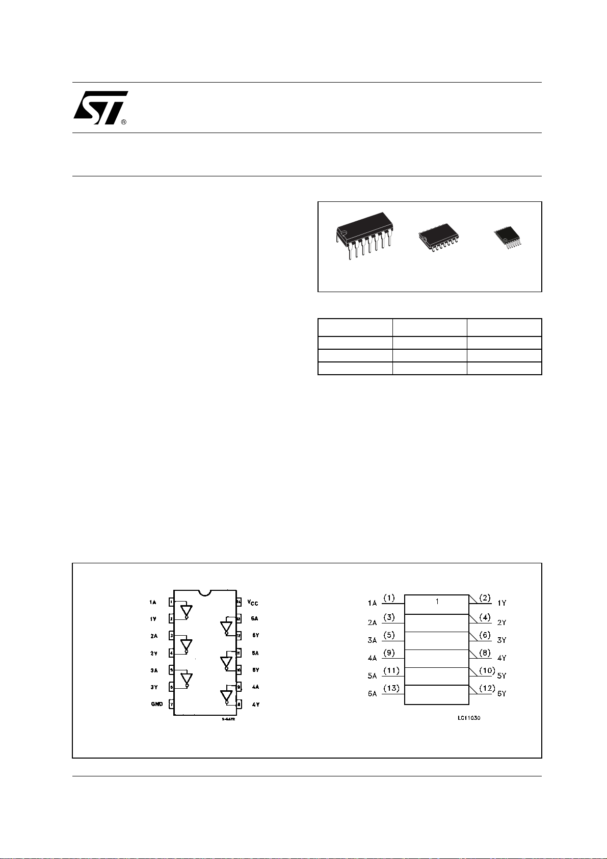
74ACT04
harman/kardon
AVR 347/230, AVR 350/230 Semiconductor Pinouts
Page 4 of 51
HEX INVERTER
■ HIGH SPEED: t
■ LOW POWER DISSIPATION:
I
= 2µA(MAX.) at TA=25°C
CC
■ COMPATI B L E WITH TTL OUTPUT S
V
= 2V (MIN.), VIL = 0.8V (MAX.)
IH
■ 50Ω TRANSMI SS ION LINE DRIVING
= 5.0ns (TYP.) at VCC = 5V
PD
CAPABILITY
■ SYMMETRICAL OUTPUT IMPEDANCE:
|I
| = IOL = 24mA (MIN)
OH
■ BALANCED PROPAGATION DELAYS:
t
≅ t
PLH
■ OPERA TING VOLTAGE RANGE:
V
CC
■ PIN AND FUNCTION COMPATIBLE WITH
PHL
(OPR) = 4.5V to 5.5V
74 SERIES 04
■ IMPROVED LATCH-UP IMMUNITY
DESCRIPTION
The 74ACT04 is an advanced high-speed CMOS
HEX INVERTER fabricated with sub-micron
silicon gate and double-layer metal wiring C
2
MOS
technology.
The internal circuit is composed of 3 stages
including buffer output , which enables high noise
immunity and stable output.
TSSOPDIP SOP
ORDER CODES
PACKAGE TUBE T & R
DIP 74ACT04B
SOP 74ACT04M 74ACT04MTR
TSSOP 74ACT04TTR
The device is designed to interface directly High
Speed CMOS systems with TTL, NMOS and
CMOS output voltage levels.
All inputs and outputs are equipped with
protection circuits against stat ic discharge, giving
them 2KV ESD immunity and transient excess
voltage.
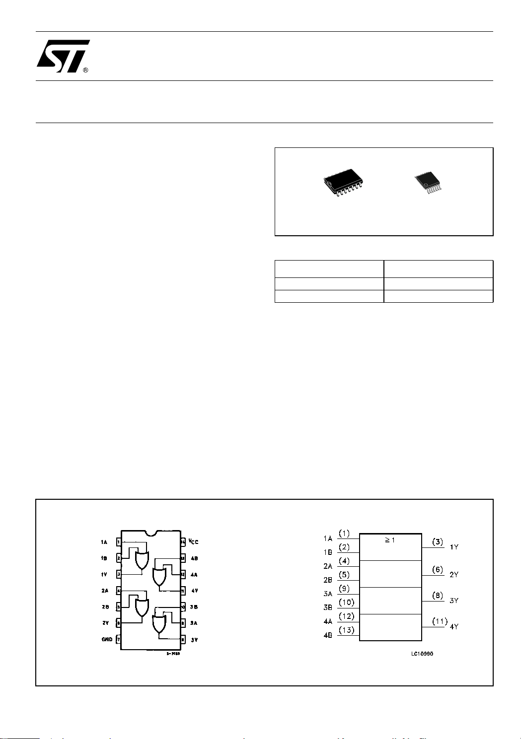
PIN CONNECTION AND IEC LOGIC SYMBOLS
1/8July 2001
Page 5
74LCX32
harman/kardon
AVR 347/230, AVR 350/230 Semiconductor Pinouts
Page 5 of 51
LOW VOLTAGE CMOS QUAD 2-INPUT OR GATE
WITH 5V TOLERANT INPUTS
■ 5V TOLERANT INPUTS
■ HIGH SPEED:
t
= 5.2ns (MAX.) at VCC = 3V
PD
■ POWER DOWN PROTECTION ON INPUTS
AND OUTPUTS
■ SYMMETRICAL OUTPUT IMPEDANCE:
|I
| = IOL = 24mA (MIN) at VCC = 3V
OH
■ PCI BUS LEVELS GUARANTEED AT 24 mA
■ BALANCED PROPAGATION DELAYS:
t
≅ t
PLH
■ OPERATI N G VOLTAGE RANGE:
V
CC
PHL
(OPR) = 2.0V to 3.6V (1.5V Data
Retention)
■ PIN AND FUNCTION COMPATIBLE WITH
74 SERIES 32
■ LATCH-UP PERFORMANCE EXCEEDS
500mA (JESD 17)
■ ESD PERFORMANCE:
HBM > 2000V (MIL STD 883 method 3015);
MM > 200V
DESCRIPTION
The 74LCX32 is a low voltage CMOS QUAD
2-INPUT OR GATE fabricated with sub-micron
silicon gate and double-layer metal wiring C
2
MOS
TSSOPSOP
Table 1: Order Codes
PACKAGE T & R
SOP 74LCX32MTR
TSSOP 74LCX32TTR
technology. It is ideal for low power and high
speed 3.3V applications; it can be interfaced to 5V
signal environment for inputs.
It has same speed performance at 3.3V than 5V
AC/ACT family, combined with a lower power
consumption.
All inputs and outputs are equipped with
protection circuits against static disc harge, giving
them 2KV ESD immunity and transient excess
voltage.
Figure 1: Pin Conne ction And IE C Logic Symbols
September 2004
Rev. 6
Page 6

LOW VOLTAGE CMOS DUAL D-TYPE FLIP FLOP
harman/kardon
AVR 347/230, AVR 350/230 Semiconductor Pinouts
Page 6 of 51
■ 5V TOLERANT INPUTS
■ HIGH SPEED :
f
= 150 MHz (MAX.) at VCC=3V
MAX
■ POWER DOWNPROTECTION ON INPUTS
AND OUTPUTS
■ SYMMETRICAL OUTPUT IMPEDANCE:
|IOH|=IOL= 24mA (MIN) at VCC=3V
■ PCI BUS LEVELS GUARANTEED AT 24 mA
■ BALANCED PROPAGATION DELAYS:
t
≅ t
PLH
PHL
■ OPERATING VOLTAGE RANGE:
VCC(OPR) = 2.0V to 3.6V (1.5V Data
Retention)
■ PIN AND FUNCTION COMPATIBLE WITH
74 SERIES 74
■ LATCH-UP PERFORMANCE EXCEEDS
500mA (JESD 17)
■ ESD PERFORMANCE:
HBM > 2000V (MIL STD 883 method 3015);
MM > 200V
DESCRIPTION
The 74LCX74 is a low voltage CMOS DUAL
D-TYPE FLIP FLOP WITH PRESET AND CLEAR
NON INVERTING fabricated with sub-micron
silicon gate and double-layer metal wiring C2MOS
technology. It is ideal for low power and high
speed 3.3V applications; it can be interfaced to 5V
signal environment for inputs.
74LCX74
WITH 5V TOLERANT INPUTS
TSSOPSOP
ORDER CODES
PACKAGE TUBE T & R
SOP 74LCX74M 74LCX74MTR
TSSOP 74LCX74TTR
A signal on the D INPUT is transferred to the Q
OUTPUT duringthe positive going transition of the
clock pulse.
CLR and PR are independent of the clock and
accomplished by a low setting on the appropriate
input.
It has same speed performance at 3.3V than 5V
AC/ACT family, combined with a lower power
consumption.
All inputs and outputs are equipped with
protection circuits against static discharge, giving
them 2KV ESD immunity and transient excess
voltage.
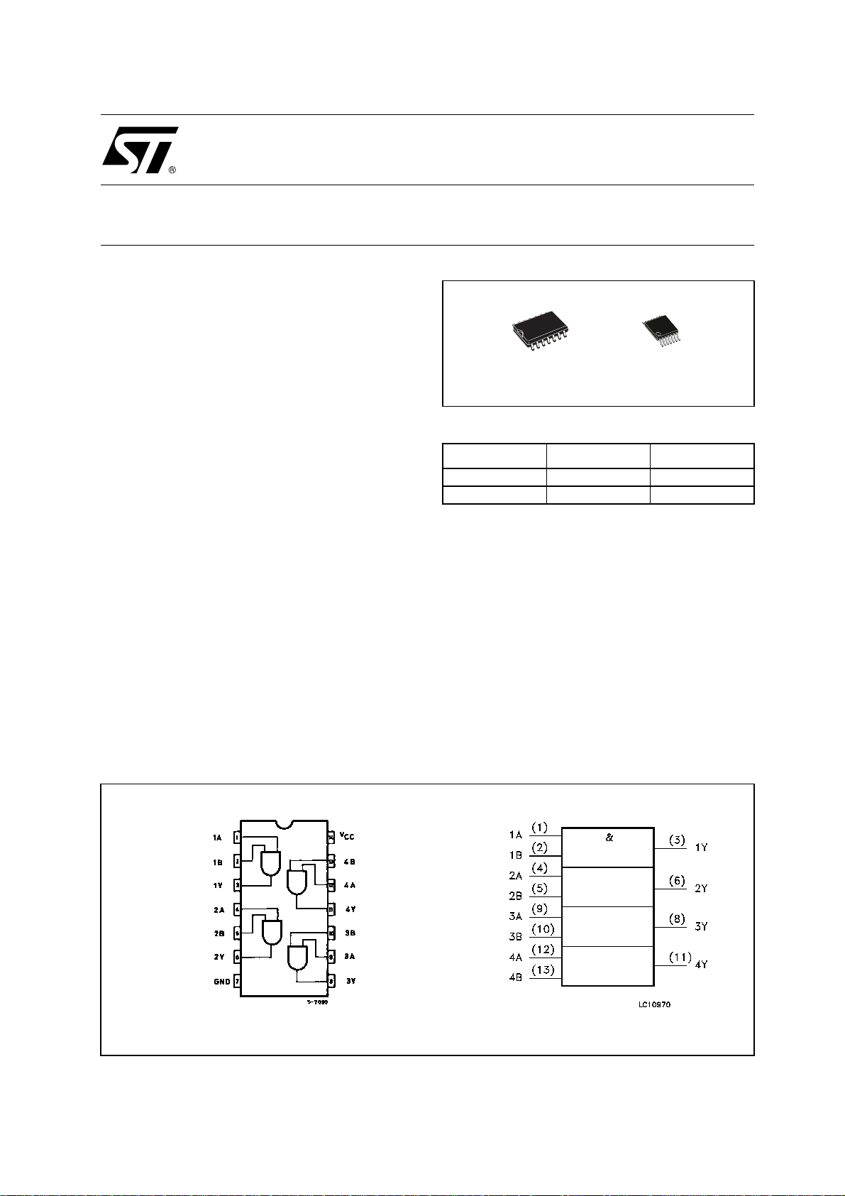
PIN CONNECTION AND IEC LOGIC SYMBOLS
1/11September 2001
Page 7
74VHC08
harman/kardon
AVR 347/230, AVR 350/230 Semiconductor Pinouts
Page 7 of 51
QUAD 2-INPUT AND GATE
■ HIGH SPEED: t
■ LOW POWER DISSIPATION:
I
= 2 µA (MAX.) at TA=25°C
CC
■ HIGH NOISE IMMUNITY:
V
= V
NIH
■ POWER DOWN PROTECTION ON INPUTS
■ SYMMETRICAL OUTPUT IMPEDANCE:
|I
| = IOL = 8mA (MIN)
OH
■ BALANCED PROPAGATION DELAYS:
t
≅ t
PLH
■ OPERATI N G VOLTAGE RANGE:
V
(OPR) = 2V to 5.5V
CC
■ PIN AND FUNCTION COMPATIBLE WITH
= 28% VCC (MIN.)
NIL
PHL
= 4.3 ns (TYP.) at VCC = 5V
PD
74 SERIES 08
■ IMPROVED LATCH-UP IMMUNITY
■ LOW NOISE: V
= 0.8V (MAX.)
OLP
DESCRIPTION
The 74VHC08 is a n advanced high-speed CM OS
QUAD 2-INPUT AND GATE fabricated with
sub-micron silicon gate and double-layer metal
wiring C
2
MOS technology.
The internal circuit is composed of 2 stages
including buffer ou tput, which provides high no ise
immunity and stable output.
TSSOPSOP
ORDER CODES
PACKAGE TUBE T & R
SOP 74VHC08M 74VHC08MTR
TSSOP 74VHC08TTR
Power down protection is provided on all inputs
and 0 to 7V can be accepted on inputs with no
regard to the supply voltage. This device can be
used to interface 5V to 3V.
All inputs and outputs are equipped with
protection circuits against stat ic discharge, giving
them 2KV ESD immunity and transient excess
voltage.
PIN CONNECTION AND IEC LOGIC SYMBOLS
June 2001
Page 8
1
2
NC = NO CONNECT
V+
NC (OR V–)
V–
3
TOP
VIEW
QUANTITY
TEMPERATURE DRIFT – ppm/°C
0
–40
5
10
15
20
25
30
35
40
45
50
–30 –20 –10
0
10 20 30 40
QUANTITY
OUTPUT ERROR – mV
0
–10
50
100
150
200
250
300
–8 –6 –4 –2 0 2 4 10
68
1.2 V Micropower, Precision
harman/kardon
AVR 347/230, AVR 350/230 Semiconductor Pinouts
Page 8 of 51
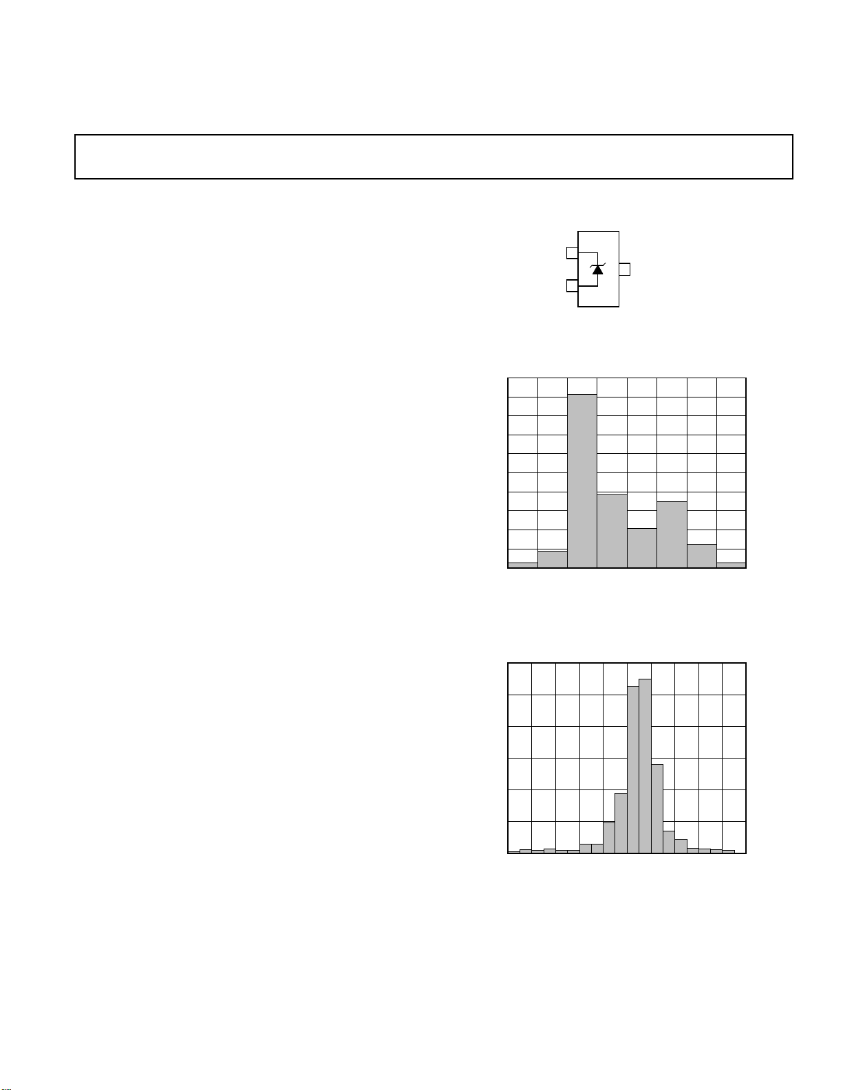
a
FEATURES
Wide Operating Range: 50 mA–10 mA
Initial Accuracy: 60.1% max
Temperature Drift: 650 ppm/8C max
Output Impedance: 0.5 V max
Wideband Noise (10 Hz–10 kHz): 20 mV rms
Operating Temperature Range: –408C to +858C
High ESD Rating
4 kV Human Body Model
400 V Machine Model
Compact, Surface-Mount, SOT-23 Package
GENERAL DESCRIPTION
The AD1580 is a low cost, two-terminal (shunt), precision
bandgap reference. It provides an accurate 1.225 V output for
input currents between 50 µA and 10 mA.
The AD1580’s superior accuracy and stability is made possible
by the precise matching and thermal tracking of on-chip
components. Proprietary curvature correction design techniques
have been used to minimize the nonlinearities in the voltage
output temperature characteristics. The AD1580 is stable with
any value of capacitive load.
The low minimum operating current makes the AD1580 ideal
for use in battery powered 3 V or 5 V systems. However, the
wide operating current range means that the AD1580 is
extremely versatile and suitable for use in a wide variety of high
current applications.
The AD1580 is available in two grades, A and B, both of which
are provided in an SOT-23 package, the smallest surface mount
package available on the market. Both grades are specified over
the industrial temperature range of –40°C to +85°C.
Shunt Voltage Reference
AD1580
PIN CONFIGURATION
SOT-23 Package
Reverse Voltage Temperature Drift Distribution
TARGET APPLICATIONS
1. Portable, Battery-Powered Equipment:
Cellular Phones, Notebook Computers, PDAs, GPS and
DMM.
2. Computer Workstations
Suitable for use with a wide range of video RAMDACs.
3. Smart Industrial Transmitters
4. PCMCIA Cards.
5. Automotive.
6. 3 V/5 V 8–12-Bit Data Converters.
REV. 0
Information furnished by Analog Devices is believed to be accurate and
reliable. However, no responsibility is assumed by Analog Devices for its
use, nor for any infringements of patents or other rights of third parties
which may result from its use. No license is granted by implication or
otherwise under any patent or patent rights of Analog Devices.
Reverse Voltage Error Distribution
© Analog Devices, Inc., 1995
One Technology Way, P.O. Box 9106, Norwood, MA 02062-9106, U.S.A.
Tel: 617/329-4700 Fax: 617/326-8703
Page 9
ADV7322 Preliminary Technical Data
harman/kardon
AVR 347/230, AVR 350/230 Semiconductor Pinouts
Page 9 of 51
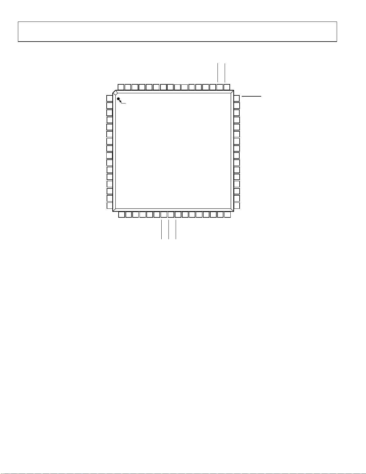
PIN CONFIGURATION AND FUNCTION DESCRIPTIONS
V
DD_IO
TEST0
TEST1
V
DGND
TEST2
TEST3
Y0
Y1
Y2
Y3
Y4
Y5
DD
Y6
Y7
C0
GND_IO63CLKIN_B62S761S660S559S458S357DGND56V
64
1
2
3
4
5
6
7
8
9
10
11
12
13
14
15
16
PIN 1
17C118C219
20
C
2
I
ALSB
DD
55S254S153S052
ADV7322
TOP VIEW
(Not to Scale)
21
22
23
24
25
26C327C428C529C630C731
SDA
SCLK
P_VSYNC
P_HSYNC
P_BLANK
Figure 19. Pin Configuration
TEST551TEST450S_HSYNC
S_VSYNC
49
48
47
46
45
44
43
42
41
40
39
38
37
36
35
34
33
32
CLKIN_A
RTC_SCR_TR
S_BLANK
R
SET1
V
REF
COMP1
DAC A
DAC B
DAC C
V
AA
AGND
DAC D
DAC E
DAC F
COMP2
R
SET2
EXT_LF
RESET
05067-019
Rev. PrA | Page 18 of 88
Page 10
Preliminary Technical Data ADV7322
harman/kardon
AVR 347/230, AVR 350/230 Semiconductor Pinouts
Page 10 of 51
Table 6. Pin Function Descriptions
Mnemonic Input/Output Function
DGND G Digital Ground.
AGND G Analog Ground.
CLKIN_A I Pixel Clock Input for HD (74.25 MHz Only, PS Only (27 MHz), SD Only (27 MHz).
CLKIN_B I
COMP1,
O Compensation Pin for DACs. Connect 0.1 µF capacitor from COMP pin to V
COMP2
DAC A O CVBS/Green/Y/Y Analog Output.
DAC B O Chroma/Blue/U/Pb Analog Output.
DAC C O Luma/Red/V/Pr Analog Output.
DAC D O
DAC E O
DAC F O
P_HSYNC
P_VSYNC
P_BLANK
S_BLANK
S_HSYNC
S_VSYNC
I Video Horizontal Sync Control Signal for HD in Simultaneous SD/HD Mode and HD Only Mode.
I Video Vertical Sync Control Signal for HD in Simultaneous SD/HD Mode and HD Only Mode.
I Video Blanking Control Signal for HD in Simultaneous SD/HD Mode and HD Only Mode.
I/O Video Blanking Control Signal for SD Only.
I/O Video Horizontal Sync Control Signal for SD Only.
I/O Video Vertical Sync Control Signal for SD Only.
Y7 to Y0 I
C7 to C0 I
S7 to S0 I SD or Progressive Scan/HDTV Input Port for Cr [Red/V] data in 4:4:4 input mode. LSB is set up on Pin S0.
RESET
R
SET1
, R
SET2
I
I
SCLK I I2C Port Serial Interface Clock Input.
SDA I/O I2C Port Serial Data Input/Output.
ALSB I
V
P Power Supply for Digital Inputs and Outputs.
DD_IO
VDD P Digital Power Supply.
VAA P Analog Power Supply.
V
I/O Optional External Voltage Reference Input for DACs or Voltage Reference Output (1.235 V).
REF
EXT_LF I External Loop Filter for the Internal PLL.
RTC_SCR_TR I Multifunctional Input. Real time control (RTC) input, timing reset input, subcarrier reset input.
I2C I This input pin must be tied high (V
GND_IO Digital Input/Output Ground.
TEST0 to
I Not used. Tie to DGND
TEST5
Pixel Clock Input. Requires a 27 MHz reference clock for progressive scan mode or a 74.25 MHz (74.1758
MHz) reference clock in HDTV mode. This clock is only used in dual modes.
.
AA
In SD Only Mode: CVBS/Green/Y Analog Output; in HD Only Mode and Simultaneous HD/SD Mode:
Y/Green [HD] Analog Output.
In SD Only Mode: Luma/Blue/U Analog Output; in HD Only Mode and Simultaneous HD/SD Mode: Pr/Red
Analog Output.
In SD Only Mode: Chroma/Red/V Analog Output; in HD Only Mode and Simultaneous HD/SD Mode:
Pb/Blue [HD] Analog Output.
SD or Progressive Scan/HDTV Input Port for Y Data. Input port for interleaved progressive scan data. The
LSB is set up on Pin Y0.
Progressive Scan/HDTV Input Port 4:4:4 Input Mode. This port is used for the Cb [Blue/U] data. The LSB is
set up on Pin C0.
This input resets the on-chip timing generator and sets the ADV7322 into default register setting.
RESET
an active low signal.
A 3040 Ω resistor must be connected from this pin to AGND and is used to control the amplitudes of the
DAC outputs.
2
TTL Address Input. This signal sets up the LSB of the I
activated, which reduces noise on the I
2
C interface.
) for the ADV7322 to interface over the I2C port.
DD_IO
C address. When this pin is tied low, the I2C filter is
is
Rev. PrA | Page 19 of 88
Page 11
Features
harman/kardon
AVR 347/230, AVR 350/230 Semiconductor Pinouts
Page 11 of 51
• Low-voltage and Standard-voltage Operation
– 2.7 (VCC = 2.7V to 5.5V)
– 1.8 (V
• Internally Organized 128 x 8 (1K), 256 x 8 (2K), 512 x 8 (4K),
1024 x 8 (8K) or 2048 x 8 (16K)
• Two-wire Serial Interface
• Schmitt Trigger, Filtered Inputs for Noise Suppression
• Bidirectional Data Transfer Protocol
• 100 kHz (1.8V) and 400 kHz (2.7V, 5V) Compatibility
• Write Protect Pin for Hardware Data Protection
• 8-byte Page (1K, 2K), 16-byte Page (4K, 8K, 16K) Write Modes
• Partial Page Writes Allowed
• Self-timed Write Cycle (5 ms max)
• High-reliability
– Endurance: 1 Million Write Cycles
– Data Retention: 100 Years
• Automotive Grade and Lead-free/Halogen-free Devices Available
• 8-lead PDIP, 8-lead JEDEC SOIC, 8-lead MAP, 5-lead SOT23,
8-lead TSSOP and 8-ball dBGA2 Packages
• Die Sales: Wafer Form, Waffle Pack and Bumped Wafers
= 1.8V to 5.5V)
CC
Two-wire
Serial EEPROM
1K (128 x 8)
2K (256 x 8)
4K (512 x 8)
8K (1024 x 8)
Description
The AT24C01A/02/04/08A/16A provides 1024/2048/4096/8192/16384 bits of serial
electrically erasable and programmable read-only memory (EEPROM) organized as
128/256/512/1024/2048 words of 8 bits each. The device is optimized for use in many
industrial and commercial applications where low-power and low-voltage operation
are essential. The AT24C01A/02/04/08A/16A is available in space-saving 8-lead PDIP,
8-lead JEDEC SOIC, 8-lead MAP, 5-lead SOT23 (AT24C01A/AT24C02/AT24C04), 8lead TSSOP, and 8-ball dBGA2 packages and is accessed via a Two-wire serial interface. In addition, the entire family is available in 2.7V (2.7V to 5.5V) and 1.8V (1.8V to
5.5V) versions.
Table 1. Pin Configuration
Pin Name Function
A0 - A2 Address Inputs
SDA Serial Data
SCL Serial Clock Input
WP Write Protect
NC No Connect
GND Ground
VCC Power Supply
8-lead TSSOP
A0
A1
A2
GND
8-ball dBGA2
VCC
WP
SCL
SDA
Bottom View
8-lead PDIP
1
2
3
4
8
VCC
7
WP
6
SCL
5
SDA
GND
1
8
7
6
5
A0
2
A1
3
A2
4
GND
A0
A1
A2
8-lead MAP
VCC
8
WP
7
SCL
6
SDA
5
Bottom View
5-lead SOT23
8-lead SOIC
1
2
3
4
1
2
3
4
8
7
6
5
A0
A1
A2
GND
VCC
WP
SCL
SDA
16K (2048 x 8)
AT24C01A
AT24C02
AT24C04
AT24C08A
AT24C16A
A0
A1
A2
GND
1
2
3
4
8
VCC
7
WP
6
SCL
5
SDA
GND
SCL
SDA
1
2
3
WP
5
VCC
4
0180V–SEEPR–8/05
1
Page 12
2. PIN DESCRIPTIONS
T
harman/kardon
AVR 347/230, AVR 350/230 Semiconductor Pinouts
Page 12 of 51
CS42528
CX_SDIN1
CX_SCLK
CX_LRCK
VD
DGND
VLC
SCL/CCLK
SDA/CDOUT
AD1/CDIN
AD0/CS
INT
RST
AINR-
AINR+
AINL+
AINL-
CX_SDIN2
CX_SDIN4
CX_SDIN3
64 63 62 61 60 59 58 57 56 55 54 53 52 51 50 49
1
2
3
4
5
6
7
8
9
10
11
12
13
14
15
16
17 18 19 20 21 22 23 24 25 26 27 28 29 30 31 32
VQ
FILT+
REFGND
OMCK
SAI_SCLK
SAI_LRCK
CS42528
VA
AOUTB4-
AOUTA4-
AOUTB4+
AOUTA4+
AGND
AOUTB3-
AOUTB3+
AOUTA3+
VLS
SAI_SDOU
RMCK
CX_SDOUT
ADCIN2
ADCIN1
DGND
AOUTA3-
VD
AOUTB2-
TXP
AOUTB2+
RXP0
AOUTA2+
48
47
46
45
44
43
42
41
40
39
38
37
36
35
34
33
RXP1/GPO1
RXP2/GPO2
RXP3/GPO3
RXP4/GPO4
RXP5/GPO5
RXP6/GPO6
RXP7/GPO7
VARX
AGND
LPFLT
MUTEC
AOUTA1-
AOUTA1+
AOUTB1+
AOUTB1-
AOUTA2-
Pin Name # Pin Description
CX_SDIN1
CX_SDIN2
CX_SDIN3
CX_SDIN4
CX_SCLK 2 CODEC Serial Clock (Input/Output) - Serial clock for the CODEC serial audio interface.
CX_LRCK 3 CODEC Left Right Clock (Input/Output) - Determines which channel, Left or Right, is currently active on
VD 451Digital Power (Input) - Positive power supply for the digital section.
DGND 552Digital Ground (Input) - Ground reference. Should be connected to digital ground.
VLC 6
SCL/CCLK 7 Serial Control Port Clock (Input) - Serial clock for the serial control port. Requires an external pull-up
SDA/CDOUT 8 Serial Control Data (Input/Output) - SDA is a data I/O line in I
AD1/CDIN 9 Address Bit 1 (I2C)/Serial Control Data (SPI) (Input) - AD1 is a chip address pin in I
1
Codec Serial Audio Data Input (Input) - Input for two’s complement serial audio data.
64
63
62
the CODEC serial audio data line.
Control Port Power (Input) - Determines the required signal level for the control port.
resistor to the logic interface voltage in I
2
C mode as shown in the Typical Connection Diagram.
2
C mode and requires an external pull-up
resistor to the logic interface voltage, as shown in the Typical Connection Diagram. CDOUT is the output
data line for the control port interface in SPI mode.
2
C mode; CDIN is
the input data line for the control port interface in SPI mode.
Page 13
CS42528
harman/kardon
AVR 347/230, AVR 350/230 Semiconductor Pinouts
Page 13 of 51
10
Address Bit 0 (I2C)/Control Port Chip Select (SPI) (Input) - AD0 is a chip address pin in I
2
C mode; CS
is the chip select signal in SPI mode.
INT 11 Interrupt (Output) - The CS42528 will generate an interrupt condition as per the Interrupt Mask register.
See “Interrupts” on page 40 for more details.
RST 12 Reset (Input) - The device enters a low power mode and all internal registers are reset to their default
settings when low.
AINRAINR+
AINL+
AINL-
VQ 17 Quiescent Voltage (Output) - Filter connection for internal quiescent reference voltage.
FILT+ 18 Positive Voltage Reference (Output) - Positive reference voltage for the internal sampling circuits.
REFGND 19 Reference Ground (Input) - Ground reference for the internal sampling circuits.
AOUT A1 +,-
AOUTB1 +,AOUT A2 +,AOUTB2 +,AOUT A3 +,AOUTB3 +,AOUT A4 +,AOUTB4 +,-
VA
VARX
AGND 2540Analog Ground (Input) - Ground reference. Should be connected to analog ground.
13
Differential Right Channel Analog Input (Input) - Signals are presented differentially to the delta-sigma
14
modulators via the AINR+/- pins.
15
Differential Left Channel Analog Input (Input) - Signals are presented differentially to the delta-sigma
16
modulators via the AINL+/- pins.
36,37
Differential Analog Output (Output) - The full-scale differential analog output level is specified in the
35,34
Analog Characteristics specification table.
32,33
31,30
28,29
27,26
22,23
21,20
24
Analog Power (Input) - Positive power supply for the analog section.
41
MUTEC 38 Mute Control (Out put) - The Mute Control pin outputs high impedance following an initial power-on con-
dition or whenever the PDN bit is set to a ‘1’, forcing the codec into power-down mode. The signal will
remain in a high impedance state as long as the part is in power-down mode. The Mute Control pin goes
to the selected “active” state during reset, muting, or if the master clock to left/right clock frequency ratio
is incorrect. This pin is intended to be used as a control for external mute circuits to prevent the clicks
and pops that can occur in any single supply system. The use of external mute circuits are not manda-
tory but may be desired for designs requiring the absolute minimum in extraneous clicks and pops.
LPFLT 39 PLL Loop Filter (Output) - An RC network should be connected between this pin and ground.
RXP7/GPO7
RXP6/GPO6
RXP5/GPO5
RXP4/GPO4
RXP3/GPO3
RXP2/GPO2
RXP1/GPO1
RXP0 49 S/PDIF Receiver Input (Input) - Dedicated receiver input for S/PDIF encoded data.
TXP 50 S/PDIF Transmitter Output (Output) - S/PDIF encoded data output, mapped directly from one of the
42
S/PDIF Receiver Input/ General Purpose Output (Input/Output) - Receiver inputs for S/PDIF encoded
43
data. The CS42528 has an internal 8:2 multiplexer to select the active receiver port, according to the
44
Receiver Mode Control 2 register. These pins can also be configured as general purpose output pins,
45
ADC Overflow indicators or Mute Control outputs according to the RXP/General Purpose Pin Control
46
registers.
47
48
receiver inputs as indicated by the Receiver Mode Control 2 register.
VLS 53 Serial Port Interface Power (Input) - Determines the required signal level for the serial port interfaces.
SAI_SDOUT
54 Serial Audio Interface Serial Data Output (Output) - Output for two’s complement serial audio PCM
data from the S/PDIF incoming stream. This pin can also be configured to transmit the output of the inter-
nal and external ADCs.
RMCK 55 Recovered Master Clock (Output) - Recovered master clock output from the External Clock Reference
(OMCK, pin 59) or the PLL which is locked to the incoming S/PDIF stream or CX_LRCK.
Page 14

CS42528
harman/kardon
AVR 347/230, AVR 350/230 Semiconductor Pinouts
Page 14 of 51
CX_SDOUT 56 CODEC Serial Dat a Output (Output) - Output for two’s complement serial audio data from the internal
and external ADCs.
ADCIN1
ADCIN2
OMCK 59 External Reference Clock (Input) - External clock reference that must be within the ranges specified in
SAI_LRCK 60 Serial Audio Interface Left/Right Clock (Input/Output) - Determines which channel, Left or Right, is
SAI_SCLK 61 Serial Audio Interface Serial Clock (Input/Output) - Serial clock for the Serial Audio Interface.
58
External ADC Serial Input (Input) - The CS42528 provides for up to two external stereo analog to digital
57
converter inputs to provide a maximum of six channels on one serial data output line when the CS42528
is placed in One Line mode.
the register “OMCK Frequency (OMCK Freqx)” on page 54.
currently active on the serial audio data line.
Page 15
3. TYPICAL CONNECTION DIAGRAM
harman/kardon
AVR 347/230, AVR 350/230 Semiconductor Pinouts
Page 15 of 51
CS42528
+3.3 V to +5 V
+2.5 V
to +5 V
+1.8 V
to +5 V
** Resistors are required for
2
I
+
10 µF
+
10 µF
Driver
S/PDIF
Interface
Up to 8
Sources
CS5361
A/D Converter
CS5361
A/D Converter
Digital Audio
Processor
Micro-
Controller
C control port operation
0.1 µF 0.01 µF
0.1 µF
OSC
** **
2 kΩ 2 kΩ
0.01 µF
0.1 µF
0.1 µF
VD
50
49
48
47
46
45
44
43
42
53
59
58
57
55
RMCK
54
60
61
3
2
56
1
64
63
62
11
12
7
8
9
10
6
4
TXP
RXP0
RXP1/GPO1
RXP2/GPO2
RXP3/GPO3
RXP4/GPO4
RXP5/GPO5
RXP6/GPO6
RXP7/GPO7
VLS
OMCK
ADCIN1
ADCIN2
51
CS42528
SAI_SDOUT
SAI_LRCK
SAI_SCLK
CX_LRCK
CX_SCLK
CX_SDOUT
CX_SDIN1
CX_SDIN2
CX_SDIN3
CX_SDIN4
INT
RST
SCL/CCLK
SDA/CDOUT
AD1/CDIN
AD0/CS
VLC
DGND
DGND
5
52 40
25
41
VAVD
24
VA
AOUTA1+
AOUTA1-
AOUTB1+
AOUTB1-
AOUTA2+
AOUTA2-
AOUTB2+
AOUTB2-
AOUTA3+
AOUTA3-
AOUTB3+
AOUTB3-
AOUTA4+
AOUTA4-
AOUTB4+
AOUTB4-
MUTEC
AINL+
AINL-
AINR+
AINR-
VQ
FILT+
REFGND
LPFLT
AGNDAGND
0.01 µF
0.01 µF
36
37
35
34
32
33
31
30
28
29
27
26
22
23
21
20
+VA
38
15
16
14
13
17
18
19
39
*
*
0.1 µF
RFILT
CFILT
0.1 µF
+
10 µF
0.1 µF
+
10 µF
Analog Output Buffer
and
Mute Circuit (optional)
Analog Output Buffer
and
Mute Circuit (optional)
Analog Output Buffer
and
Mute Circuit (optional)
Analog Output Buffer
and
Mute Circuit (optional)
Analog Output Buffer
and
Mute Circuit (optional)
Analog Output Buffer
and
Mute Circuit (optional)
Analog Output Buffer
and
Mute Circuit (optional)
Analog Output Buffer
and
Mute Circuit (optional)
Mute
Drive
(optional)
Analog
2700 pF*
Input
1
Buffer
Analog
Input
2700 pF*
1
Buffer
+
3
3
100 µF
CRIP
0.1 µF
3
+5 V
2
2
2
2
2
2
2
2
* Pull up or down as
required on startup if the
Mute Control is used.
Left Analog Input
Right Analog Inpu
+
4.7 µF
1. See the ADC Input Filter section in the Appendix.
2. See the DAC Output Filter section in the Appendix.
3. See the PLL Filter section in the Appendix.
20 DS586PP5
Connect DGND and AGND at single point near Codec
Figure 5. Typical Connection Diagram
Page 16
harman/kardon
AVR 347/230, AVR 350/230 Semiconductor Pinouts
Page 16 of 51
Page 17

harman/kardon
AVR 347/230, AVR 350/230 Semiconductor Pinouts
Page 17 of 51
PIN DESCRIPTION
Pin Description
A0-A18 19 Addresses
DQ0-DQ14 15 Data Inputs/Outputs
DQ15/A-1
CE# Chip Enable
OE# Output Enable
WE# Write Enable
RESET# Hardware Reset Pin, Active Low
BYTE# Selects 8-bit or 16-bit mode
RY/BY# Ready/Busy Output
Vcc
Vss Device Ground
NC Pin Not Connected Internally
Excel Semiconductor inc.
DQ15 (Data Input/Output, Word Mode)
A-1 (LSB Address Input, Byte Mode)
3.0 volt-only single power supply
(see Product Selector Guide for speed options and voltage supply tolerances)
LOGIC SYMBOL
19
A0 ~ A18
CE#
OE#
WE#
RESET#
BYTE#
16 or 8
DQ0 ~ DQ15
(A-1)
RY/BY#
Page 18

harman/kardon
AVR 347/230, AVR 350/230 Semiconductor Pinouts
Page 18 of 51
CONNECTION DIAGRAM
Excel Semiconductor inc.
A15
A14
A13
A12
A11
A10
A9
A8
NC
NC
WE#
RESET#
NC
NC
RY/BY#
A18
A17
A7
A6
A5
A4
A3
A2
A1
1
2
3
4
5
6
7
8
9
10
11
12
13
14
15
16
17
18
19
20
21
22
23
24
48-Pin Standard TSOP
ES29LV800
48
47
46
45
44
43
42
41
40
39
38
37
36
35
34
33
32
31
30
29
28
27
26
25
A16
BYTE#
Vss
DQ15/A-1
DQ7
DQ14
DQ6
DQ13
DQ5
DQ12
DQ4
Vcc
DQ11
DQ3
DQ10
DQ2
DQ9
DQ1
DQ8
DQ0
OE#
Vss
CE#
A0
48-Ball FBGA (6 x 8 mm)
(Top View, Balls Facing Down)
A B C D E F G H
6
5
4
3
2
1
A13 A12
A9
WE#
RY/
BY#
A7
A3
A8
RESET#
NC
A17
A4
A14
A10
NC
A18
A6
A2
A15
A16
A11 DQ7
NC
NC
A5
DQ5
DQ2
DQ0
A0A1
BYTE#
DQ14
DQ12
DQ10 DQ11 DQ3
DQ8 DQ9 DQ1
DQ15/
A-1
DQ13
Vcc
OE#CE#
Vss
DQ6
DQ4
Vss
Page 19

ANALOG MULTIPLEXER/DEMULTIPLEXER
harman/kardon
AVR 347/230, AVR 350/230 Semiconductor Pinouts
Page 19 of 51
■ LOW "O N" RESISTANCE : 125Ω (Typ.)
OVER 15V p.p SIGNA L-INPU T RANGE FOR
V
DD-VEE
■ HIGH "OFF" RESISTANCE : CHANNEL
LEAKAGE ± 100pA (Typ.) at V
■ BINARY ADDRESS DECODING ON CHIP
■ HIGH DEGREE OF LINEARITY : < 0.5%
DISTORTIONTYP. at f
V
DD-VSS
■ VERY LOW QUIESCENT POWER
DISSIPATION UNDER ALL DIGITAL
CONTROL INPUT AND SUPPLY
CONDITIONS : 0.2
at V
■ MATCHED SWITCH CHARACTERISTICS :
R
ON
■ WIDE RANGE O F DIGITAL AND ANALOG
SIGNAL LEVELS : DIGITAL 3 to 20,
ANALOG TO 20V p.p.
■ QUIESCENT CURRENT SPECIF. UP TO 20V
■ 5V, 10V AND 15V PARAMETRIC RATINGS
■ INPUT LEAKAGE CURRENT
I
= 100nA (MAX) AT VDD=18VTA= 25°C
I
■ 100% TESTED FOR QUIESCENT CURRENT
■ MEETS ALL REQUIREMENTS OF JEDEC
JESD13B " STANDARD SPECIFICATIONS
FOR DESCRIPTIONOF B SERIES CMOS
DEVICES"
DESCRIPTION
The HCF4053B is a monolithic integrated circuit
fabricated in Metal Oxide Semiconductor
= 15V
DD-VEE
=1KHz,VIS=5Vpp,
IS
> 10V, RL = 10KΩ
µW(Typ.)
DD-VSS=VDD-VEE
=10V
=5Ω (Typ.) FOR VDD-VEE= 15V
=18V
HCF4053B
TRIPLE 2-CHANNEL
DIP SOP
ORDER CODES
PACKAGE TUBE T & R
DIP HCF4053BEY
SOP HCF4053BM1 HCF4053M013TR
technology available in DIP and SOP packages.
The HCF4053B analog multiplexer/demultiplexer
is a digitally controlled analog switch having low
ON impedance and very low OFF leakage current.
This multiplexer circuit dissipate extremely low
quiescent power over the f ull V
V
supply voltage rang e, independent of the
EE
DD-VSS
logic state of the control signals.
When a logic "1" is present at the inhibit input
terminal all channel are off. This device is a triple
2-channel multiplexe r having three separate
digital c ontrol input s, A, B, and C, and an inhibit
input. Each control input selects one of a pair of
channels which are connected in a single pole
double-throw configuration.
and VDD-
PIN CONNECTION
October 2002
Page 20

harman/kardon
AVR 347/230, AVR 350/230 Semiconductor Pinouts
Page 20 of 51
Page 21

Pin Assignment (DIP16/MFP16)
No. 6037-2/8
LC72723, LC72723M
Block Diagram
harman/kardon
AVR 347/230, AVR 350/230 Semiconductor Pinouts
Page 21 of 51
Page 22

PIN CONFIGURATION
harman/kardon
AVR 347/230, AVR 350/230 Semiconductor Pinouts
Page 22 of 51
V
V
DD
DD
DQ0
DQ0
DQ1
DQ1
V
V
SSQ
SSQ
DQ2
DQ2
DQ3
DQ3
V
V
DDQ
DDQ
DQ4
DQ4
DQ5
DQ5
V
V
SSQ
SSQ
DQ6
DQ6
DQ7
DQ7
VDDQ
VDDQ
LDQM
LDQM
/WE
/WE
/CAS
/CAS
/RAS
/RAS
/CS
/CS
A11
A11
A10
A10
A0
A0
A1
A1
A2
A2
A3
A3
V
V
DD
DD
1
1
2
2
3
3
4
4
5
5
6
6
7
7
8
8
9
9
10
10
11
11
12
12
13
13
14
14
15
15
16
16
17
17
18
18
19
19
20
20
21
21
22
22
23
23
24
24
25
25
50pin TSOP II
50pin TSOP II
400mil x 825mil
400mil x 825mil
0.8mm pin pitch
0.8mm pin pitch
50
50
49
49
48
48
47
47
46
46
45
45
44
44
43
43
42
42
41
41
40
40
39
39
38
38
37
37
36
36
35
35
34
34
33
33
32
32
31
31
30
30
29
29
28
28
27
27
26
26
V
V
SS
SS
DQ15
DQ15
DQ14
DQ14
VSSQ
VSSQ
DQ13
DQ13
DQ12
DQ12
VDDQ
VDDQ
DQ11
DQ11
DQ10
DQ10
VSSQ
VSSQ
DQ9
DQ9
DQ8
DQ8
VDDQ
VDDQ
NC
NC
UDQM
UDQM
CLK
CLK
CKE
CKE
NC
NC
A9
A9
A8
A8
A7
A7
A6
A6
A5
A5
A4
A4
VSS
VSS
PIN DESCRIPTION
PIN PIN NAME DESCRIPTION
CLK Clock
CKE Clock Enable
CS
BA Bank Address Select either one of banks during both RAS
A0 ~ A10 Address
, CAS, WE
RAS
LDQM, UDQM Data Input/Output Mask DQM control output buffer in read mode and mask input data in write mode
DQ0 ~ DQ15 Data Input/Output Multiplexed data input / output pin
DD/VSS Power Supply/Ground Power supply for internal circuit and input buffer
V
DDQ/VSSQ Data Output Power/Ground Power supply for DQ
V
NC No Connection No connection
Chip Select Command input enable or mask except CLK, CKE and DQM
Row Address Strobe,
Column Address Strobe, Write
Enable
The system clock input. All other inputs are referenced to the SDRAM on the rising
edge of CLK.
Controls internal clock signal and when deactivated, the SDRAM will be one of the
states among power down, suspend or self refresh.
and CAS activity.
Row Address : RA0 ~ RA10, Column Address : CA0 ~ CA7
Auto-precharge flag : A10
, CAS and WE define the operation.
RAS
Refer function truth table for details
Page 23

harman/kardon
AVR 347/230, AVR 350/230 Semiconductor Pinouts
Page 23 of 51
Page 24

harman/kardon
AVR 347/230, AVR 350/230 Semiconductor Pinouts
Page 24 of 51
Page 25

harman/kardon
AVR 347/230, AVR 350/230 Semiconductor Pinouts
Page 25 of 51
Page 26

Figure 3: Connection Diagram (top view)
harman/kardon
AVR 347/230, AVR 350/230 Semiconductor Pinouts
Page 26 of 51
L7800 SERIES
TO-220 (Any Type)
2
PAK (Any Ty p e )
TO-220FP/TO-220FM
TO-3D
Table 3: Order Codes
2
PAK
TYPE
L7805 L7805T
L7805C L7805CV L7805C-V L7805CV1 L7805CD2T L7805C-D2TR L7805CP L7805CF L7805CT
L7852C L7852CV L7852CD2T L7852CP L7852CF L7852CT
L7806 L7806T
L7806C L7806CV L7806C-V L7806CD2T L7806CP L7806CF L7806CT
L7808 L7808T
L7808C L7808CV L7808C-V L7808CD2T L7808CP L7808CF L7808CT
L7885C L7885CV L7885CD2T L7885CP L7885CF L7885CT
L7809C L7809CV L7809C-V L7809CD2T L7809CP L7809CF L7809CT
L7810C L7810CV L7810CD2T L7810CP
L7812 L7812T
L7812C L7812CV L7812C-V L7812CD2T L7812CP L7812CF L7812CT
L7815 L7815T
L7815C L7815CV L7815C-V L7815CD2T L7815CP L7815CF L7815CT
L7818 L7818T
L7818C L7818CV L7818CD2T L7818CP L7818CF L7818CT
L7820 L7820T
L7820C L7820CV L7820CD2T L7820CP L7820CF L7820CT
L7824 L7824T
L7824C L7824CV L7824CD2T L7824CP L7824CF L7824CT
(*) Avai l abl e in Tape & Re el wi th the suffix "-T R".
TO-220
(A Typ e)
TO-220
(C Type)
TO-220
(E Type)
2
D
PAK
(A Type) (*)
D
(C Type)
(T & R)
TO-220FP TO-220FM TO-3
Page 27

L7900
harman/kardon
AVR 347/230, AVR 350/230 Semiconductor Pinouts
Page 27 of 51
ABSOLUTE MAXIMUM RATINGS
Symbol Parameter Value Unit
DC InputVoltage (for VO= 5 to 18V)
V
i
OutputCurrent Internally limited
I
o
PowerDissipation Internally limited
P
tot
T
Operating Junction TemperatureRange 0 to 150
op
Storage Temperature Range - 65 to 150
T
stg
(forV
= 20,24V)
O
THERMALDATA
Symbol Parameter D2PAK TO-220 ISOWATT220 TO-3 Unit
R
thj-cas e
R
thj-amb
Thermal Resistance Junction-case Max
Thermal Resistance Junction-ambient Max
3
62.5
50
3
60
CONNECTION DIAGRAM AND ORDERING NUMBERS(top view)
-35
-40
4
4
35
o
o
V
V
o
C
o
C
C/W
C/W
TO-220 & ISOWATT220 TO-3D2PAK
Type TO-220 D
L7905C
L7952C
L7906C
L7908C
L7912C
L7915C
L7918C
L7920C
L7922C
L7924C
(*) AVAILABLE IN TAPE AND REEL WITH ”-TR” SUFFIX
L7905CV
L7952CV
L7906CV
L7908CV
L7912CV
L7915CV
L7918CV
L7920CV
L7922CV
L7924CV
2
L7905CD2T
L7952CD2T
L7906CD2T
L7908CD2T
L7912CD2T
L7915CD2T
L7918CD2T
L7920CD2T
L7922CD2T
L7924CD2T
APPLICATION CIRCUIT
PAK (*) ISOWATT220 TO-3 Output Voltage
L7905CP
L7906CP
L7908CP
L7912CP
L7915CP
L7918CP
L7920CP
L7924CP
L7905CT
L7952CT
L7906CT
L7908CT
L7912CT
L7915CT
L7918CT
L7920CT
L7922CT
L7924CT
-5V
-5.2V
-6V
-8V
-12V
-15V
-18V
-20V
-22V
-24V
2/13
Page 28

1A LOWDROP OUT VOLTAGE REGULATOR (ADJUSTABLE & FIXED) LM1117
harman/kardon
AVR 347/230, AVR 350/230 Semiconductor Pinouts
Page 28 of 51
FEATURES
SOT-223 PKG (FRONT VIEW)
● Output Current up to 1 A
● Low Dropout Voltage ( 700mV at 1A Output Current )
● Three Terminal Adjustable or Fixed 1.5V, 1.8V, 2.5V, 2.85V,
3.0V, 3.3V, 5.0V
● 2.85V Device for SCSI-II Active Terminator
● 0.04% Line Regulaion, 0.1% Load Regulation
1 2 3
PIN FUNCTION
1. Adj/Gnd
2. Vout
3. Vin
● Very Low Quiescent Current
● Internal Current andTerminal Limit
● Logic-Controlled Electronics Shutdown
TO-263 (D2 PKG, FRONT VIEW)
● Surface Mount Package SOT-223 & TO-263 (D2-Pack)
● 100% Thermal Limit Burn-In
PIN FUNCTION
APPLICATION
1. Adj/Gnd
2. Vout
3. Vin
● Active SCSI Terminators
● Portable/Plan Top/Notebook Computers
● High Efficiency Linear Regulators
● SMPS Post Regulators
● Mother B/D Clock Supplies
● Disk Drives
● Battery Chargers
DESCRIPTION
1 2 3
ORDERING INFORMATION
Device (Marking)
LM1117S
LM1117S-XX
LM1117T
LM1117T-XX
(X=Output Voltage=1.5V, 1.8V, 2.5V, 2.85V,
'3.0V, 3.3V, 5.0V, Adjustable=AD)
Package
SOT-223
TO-263 (D2)
The LM1117 is a low power positive-voltage regulator designed to meet 1A output current and comply
with SCSI-II specifications with a fixed output voltage of 2.85V. This device is an excellent choice for use
in battery-powered applications, as active terminators for the SCSI bus, and portable computers.
The LM1117 features very low quiescent current and very
low dropout voltage of 700mV at a full load and
lower as output current decreases. LM1117 is available as an adjustable or fixed 1.5V, 1.8V, 2.5V, 2.85V,
3.0V, 3.3V, and 5.0V output voltages.
The LM1117 is offered in a 3-pin surface mount package SOT-223 & TO-263. The output capacitor of
10㎌ or larger is needed for output stability of LM1117 as required by most of the other regulator circuits.
ABSOLUTE MAXIMUM RATINGS
CHARACTERISTIC
DC Input Voltage
Lead Temperature (Soldering, 5 Seconds)
Storage Temperature Range
Operating Junction Temperature Range
SYMBOL
V
IN
T
SOL
T
STG
T
OPR
MIN. UNIT
-65 150
0
MAX.
7
260
125
V
℃
℃
℃
HTC
1
Page 29

M24C64, M24C32
harman/kardon
AVR 347/230, AVR 350/230 Semiconductor Pinouts
Page 29 of 51
SUMMARY DESCRIPTION
These I2C-compatible electrically erasable programmable memory (EEPROM) devices are organized as 8192 x 8 bits (M24C64) and 4096 x 8 bits
(M24C32).
Table 2. Signal Names
E0, E1, E2 Chip Enable
SDA Serial Data
Figure 2. Logic Diagram
V
CC
3
E0-E2 SDA
SCL
WC
2
I
C uses a two-wire serial interf ace, comprisi ng a
M24C64
M24C32
V
SS
AI01844B
bi-directional data line and a clock line. The devices carry a built-in 4-bit Device Type Identifier code
(1010) in accordance with the I
The device behaves as a slave in the I
2
C bus definition.
2
C protocol,
with all memory operations synchronized by the
serial clock. Read and Write operations are initiated by a Start condition, generated by the bus master. The Start condition is followed by a Device
Select Code and Read/Write
bit (RW) (as described in Table 3.), terminated by an acknowledge bit.
When writing data to the memory, the dev ice inserts an acknowled ge bit during the 9
th
bit time,
following the bus master’s 8-bit transmission.
When data is read by the bus master, the bus
master acknowledge s the rec eipt o f the d ata by te
in the same way. Data transfers are terminated by
a Stop condition after an Ack for Write, and after a
NoAck for Read.
SCL Serial Clock
WC
V
CC
V
SS
Power On Reset: V
Write Control
Supply Voltage
Ground
Lock-Out Write Protect
CC
In order to prevent data corruption and inadvertent
Write operations during Power-up, a Power On
Reset (POR) circuit is included . At Power-up, the
internal reset i s he ld a cti ve unti l V
has reached
CC
the Power On Reset (POR) threshold voltage, and
all operations are disabled – the device will not respond to any command. In the sam e way, when
V
drops from the operat ing voltage, below the
CC
Power On Reset (PO R) threshold voltage, a ll operations are disa bled and the device will not respond to any command.
A stable and valid V
(as defined in Table 9. and
CC
Table 10.) must be applied before applying any
logic signal.
Figure 3. DIP, SO, TSSOP and UFDFPN
Connections
M24C64
M24C32
AI01845C
8
CC
7
WCE1
6
SCL
5
SDAV
1
E0 V
2
3
E2
4
SS
Note: See PACKAGE MECHANICAL section for package dimen-
sions, and how to identify pin-1.
Page 30

www.fairchildsemi.com
harman/kardon
AVR 347/230, AVR 350/230 Semiconductor Pinouts
Page 30 of 51
MC78XX/LM78XX/MC78XXA
3-Terminal 1A Positive Voltage Regulator
Features
• Output Current up to 1A
• Output Voltages of 5, 6, 8, 9, 10, 12, 15, 18, 24V
• Thermal Overload Protection
• Short Circuit Protection
• Output Transistor Safe Operating Area Protection
Description
The MC78XX/LM78XX/MC78XXA series of three
terminal positive regulators are available in the
TO-220/D-PAK package and with several fixed output
voltages, making them useful in a wide range of
applications. Each type employs internal current limiting,
thermal shut down and safe operating area protection,
making it essentially indestructible. If adequate heat sinking
is provided, they can deliver over 1A output current.
Although designed primarily as fixed voltage regulators,
these devices can be used with external components to
obtain adjustable voltages and currents.
TO-220
1
D-PAK
1
1. Input 2. GND 3. Output
Internal Block Digram
©2001 Fairchild Semiconductor Corporation
Rev. 1.0.1
Page 31

harman/kardon
AVR 347/230, AVR 350/230 Semiconductor Pinouts
Page 31 of 51
Page 32

harman/kardon
AVR 347/230, AVR 350/230 Semiconductor Pinouts
Page 32 of 51
Page 33

312
harman/kardon
AVR 347/230, AVR 350/230 Semiconductor Pinouts
Page 33 of 51
LOW DROPOUT VOLTAGE REGULATOR
GENERAL DESCRIPTION PACKAGE OUTLINE
The NJM2391 is low dropout voltage regulators
featuring high precision voltage.
It is suitable for Notebook PCs, PC cards and hard
disks where 3.3V need to be generated from 5V supply.
A small TO-252 package is adopted for the space
saving.
FEATURES
zOutput Current Io(max.)=1A
zHigh Precision Output Voltage Vo±1%
zLow Dropout Voltage ∆ V
=1.1V typ. At Io=1A
I-O
zInternal Excessive Voltage Protection Circuit
zInternal Short Circuit Current Limit
zInternal Thermal Overload Protection
zBipolar Technology
zPackage Outline TO-252
PIN CONFIGURATION
PIN FUNCTION
1.V
IN
2.GND
3.V
OUT
NJM2391DL1
NJM2391
NJM2391DL1
ABSOLUTE MAXIMUM RATINGS (Ta=25°C)
PARAMETER SYMBOL RATINGS UNIT
Input Voltage V+ +10 V
Power Dissipation PD TO-252
Operating Temperature
Storage Temperature
Topr
Ts tg
8 (Tc=25°C)
0.8(Ta≤25°C)
W
−40 ~ +85 °C
−50 ~ +125 °C
OUTPUT VOLTAGE RANK LIST
Device Name V
OUT
NJM2391DL1-25 2.5V
NJM2391DL1-26 2.6V
NJM2391DL1-28 2.85V
NJM2391DL1-03 3.0V
NJM2391DL1-33 3.3V
NJM2391DL1-35 3.5V
NJM2391DL1-05 5.0V
Page 34

harman/kardon
AVR 347/230, AVR 350/230 Semiconductor Pinouts
Page 34 of 51
NJM2595
5-INPUT 3-OUTPUT VIDEO SWITCH
■ GENERAL DESCRIPTION ■ PACKAGE OUTLINE
The NJM2595 is a 5-input 3-output video switch. Its switches
select one from five signals received from VTR,TV,DVD,
TV-GAME and others.
The NJM2595 is designed for audio items, such as AV amplifier
and others.
NJM2595D NJM2595M
■ FEATURES
● 5-input 3-output
● Operating Voltage ±4.0 to ±6.5V
● Operating current ±15mAtyp. at Vcc=±5V
● Crosstalk -65dBtyp.
● Internal 6dB Amplifier
● Internal 75Ω Driver
● Bipolar Technology
● Package Outline DIP16,DMP16
■ PIN CONFIGURATION and BLOCK DIAGRAM
16
+
SW2V
10 14 2
SW1
SW5
Vin1
Vin2
Vin3
Vin4
Vin5
13
20k
20k
20k
S5
S6
S7
6dB
Amp
6dB
Amp
6dB
Amp
8 12 6 4
-
75Ω
Driver
75Ω
Driver
75Ω
Driver
1
15
11
Vout1
Vout2
Vout3
9
20k
7
20k
5
20k
3
20k
S2
S3
SW3
S4
SW4
S1
GND V
Page 35

3
2
8
3 4
5
3
harman/kardon
AVR 347/230, AVR 350/230 Semiconductor Pinouts
Page 35 of 51
NJM2845/46
LOW DROPOUT VOLTAGE REGULA TOR
GENERAL DESCRIPTION PACKAGE OUTLINE
The NJM2845 is low dropout voltage regulator. Advanced
Bipolar technology achieves low noise, high ripple rejection
and low quiescent current.
NJM2845 is 3 terminal type and NJM2846 is ON/OFF control
built in type. These product can be selected according to the
applications.
FEATURES
High Ripple Rejection 75dB typ. (f=1kHz,3V Version)
Output Noise Voltage Vno=45µVrms typ. (Vo=3V Version)
Output capacitor with 2.2µF ceramic capacitor (Vo≥2.6V)
Output Current Io(max.)=800mA
High Precision Output Vo ±1.0%
Low Dropout Voltage 0.18V typ. (Io=500mA)
ON/OFF Control (NJM2846)
Internal Short Circuit Current Limit
Internal Thermal Overload Protection
Bipolar Technology
Package Outline TO-252-3 (NJM2845DL1), TO-252-5 (NJM2846DL3)
PIN CONFIGURATION
1.V
IN
2.GND
3.V
OUT
1.CONTROL
2.V
IN
3.GND
4.Vo
1
1
2
5.NC
NJM2845DL1
NJM2846DL3
NJM2845DL1 NJM2846DL3
EQUIVALENT CIRCUIT
V
GND
IN
Thermal
Protection
Bandgap
Reference
V
OUT
V
Control
GND
IN
NJM2845DL1
Ver.2005-01-20
Bandgap
Reference
NJM2
Thermal
Protection
46DL3
V
OUT
Page 36

harman/kardon
AVR 347/230, AVR 350/230 Semiconductor Pinouts
Page 36 of 51
Page 37

harman/kardon
AVR 347/230, AVR 350/230 Semiconductor Pinouts
Page 37 of 51
Page 38

harman/kardon
AVR 347/230, AVR 350/230 Semiconductor Pinouts
Page 38 of 51
Page 39

harman/kardon
AVR 347/230, AVR 350/230 Semiconductor Pinouts
Page 39 of 51
Page 40

harman/kardon
AVR 347/230, AVR 350/230 Semiconductor Pinouts
Page 40 of 51
Page 41

•
TO-92
PIN CONFIGURATION
•
SOT-89
•
SOT-23-5
PIN DESCRIPTION
•
TO-92
•
SOT-89
•
SOT-23-5
Pin No Symbol
1 OUT
2 VDD
3 GND
4 NC
5 NC
Pin No Symbol
1 OUT
2 VDD
3 GND
Pin No Symbol
1 OUT
2 VDD
3 GND
R×5VL
harman/kardon
AVR 347/230, AVR 350/230 Semiconductor Pinouts
Page 41 of 51
(mark side)
1 2
3
(mark side)
1 2
5
4
(mark side)
3
1 2
3
Page 42

RN5RZ
3
PIN CONFIGURATION
PIN DESCRIPTION
• SOT-23-5
1 2
3
5 4
(mark side)
Pin No. Symbol Description
1 GND Ground Pin
2 VDD
Input Pin
3 VOUT Output Pin
4 NC No Connection
5 CE or CE Chip Enable Pin
ABSOLUTE MAXIMUM RATINGS
ABSOLUTE MAXIMUM RATINGS
Absolute Maximum ratings are threshold limit values that must not be exceeded even for an instant under
any conditions. Moreover, such values for any two items must not be reached simultaneously. Operation
above these absolute maximum ratings may cause degradation or permanent damage to the device. These
are stress ratings only and do not necessarily imply functional operation below these limits.
Symbol Item Ratings Unit
VIN Input Voltage 9 V
VCE Input Voltage (CE or CE Pin) –0.3 to VIN +0.3 V
VOUT Output Voltage –0.3 to VIN +0.3 V
IOUT Output Current 200 mA
PD Power Dissipation 250 mW
Topt Operating Temperature –40 to +85 ˚C
Tstg Storage Temperature –55 to +125 ˚C
harman/kardon
AVR 347/230, AVR 350/230 Semiconductor Pinouts
Page 42 of 51
Page 43

harman/kardon
AVR 347/230, AVR 350/230 Semiconductor Pinouts
Page 43 of 51
Page 44

SiI 9031 HDMI PanelLink Cinema Receiver
harman/kardon
AVR 347/230, AVR 350/230 Semiconductor Pinouts
Page 44 of 51
Data Sheet
Pin Diagram
DGND
DVCC18
IOGND
IOVCC
MUTEOUT
SPDIF
CVCC
CGND
SD3
SD2
SD1
SD0
SCK
MCLKIN
MCLKOUT
IOVCC
IOGND
CGND
CVCC18
AUDPVCC18
AUDPGND
XTALOUT
XTALIN
XTALVCC
REGVCC
RSVDL
RESET#
SCDT
CVCC18
CGND
CLK48B
IOGND
WS
NC
NC
INT
73
74
75
76
77
78
79
80
81
82
83
84
85
86
87
88
89
90
91
92
93
94
95
96
97
98
99
100
101
102
103
104
105
106
107
108
AGND
72
AGND
R1X2-
R1X2+
AVCC
71
70
68
69
AGND
R1X1-
R1X1+
AVCC
65
67
66
64
AVCC
R1X0-
AGND
R1X0+
63
61
62
AVCC
R1XC+
R1XC-
58
60
59
57
AGND
PVCC1
RSVD_A
56
R0X2+
R0X2-
AGND
TMDSPGND
54
55
AVCC
50
52
53
51
49
AGND
R0X1-
R0X1+
AVCC
R0X0+
46
48
44
47
45
SiI 9031
144-Pin
TQFP
(Top View)
R0XC+
R0X0-
43
AVCC
42
R0XC-
PVCC0
AVCC
AGND
38
37
40
41
39
36
DGND
35
DVCC18
34
R0PWR5V
33
R1PWR5V
32
DSCL0
31
DSDA0
DSCL1
30
DSDA1
29
CSCL
28
27
CSDA
26
IOVCC
25
IOGND
CGND
24
CVCC18
23
22
DACDVCC18
21
DACDGND
AnBPb
20
DACVCCB
19
18
DACGNDB
AnGY
17
DACVCCG
16
DACGNDG
15
14
AnRPr
DACVCCR
13
DACGNDR
12
COMP
11
RSET
10
VREF
9
8
DACAGND
DACAVCC
7
6
DACOVCC
5
IOVCC
IOGND
4
3
VSYNC
2
HSYNC
DE
1
109
IOVCC
113
111
110
112
Q23
Q21
Q22
Q20
Individual pin functions are described beginning on page 37.
SiI-DS-0118-A 8
117
115
114
116
118
Q17
Q19
Q18
CGND
CVCC18
122
119
120
121
Q16
ODCK
IOVCC
IOGND
126
124
123
125
Q15
Q13
Q14
Q12
127
CGND
130
128
129
Q11
Q10
CVCC18
134
132
131
133
Q8
Q7
Q9
IOVCC
138
136
135
137
Q5
Q6
CGND
IOGND
142
140
139
Q4
CVCC18
144
141
143
Q3
Q2
Q1
Q0
Figure 1. Pin Diagram
Page 45

8 Mbit SPI Serial Flash
harman/kardon
AVR 347/230, AVR 350/230 Semiconductor Pinouts
Page 45 of 51
SST25VF080B
PIN DESCRIPTION
Data Sheet
CE#
SO
WP#
V
SS
1
2
Top View
3
4
1296 08-soic S2A P1.0
8
V
DD
7
HOLD#
6
SCK
5
SI
CE#
SO
WP#
V
SS
1
2
Top View
3
4
1296 08-wson QA P2.0
8
7
6
5
V
DD
HOLD#
SCK
SI
8-LEAD SOIC 8-CONTACT WSON
FIGURE 1: PIN ASSIGNMENTS
TABLE 1: PIN DESCRIPTION
Symbol Pin Name Functions
SCK Serial Clock To provide the timing of the serial interface.
Commands, addresses, or input data are latched on the rising edge of the clock input,
while output data is shifted out on the falling edge of the clock input.
SI Serial Data Input To transfer commands, addresses, or data serially into the device.
Inputs are latched on the rising edge of the serial clock.
SO Serial Data Output To transfer data serially out of the device.
Data is shifted out on the falling edge of the serial clock.
Outputs Flash busy status during AAI Programming when reconfigured as RY/BY# pin.
See “Hardware End-of-Write Detection” on page 12 for details.
CE# Chip Enable The device is enabled by a high to low transition on CE#. CE# must remain low for the
duration of any command sequence.
WP# Write Protect The Write Protect (WP#) pin is used to enable/disable BPL bit in the status register.
HOLD# Hold To temporarily stop serial communication with SPI flash memory without resetting the
device.
V
DD
V
SS
Power Supply To provide power supply voltage: 2.7-3.6V for SST25VF080B
Ground
T1.0 1296
©2006 Silicon Storage Technology, Inc. S71296-01-000 1/06
3
Page 46

ST202E/ST232E
harman/kardon
AVR 347/230, AVR 350/230 Semiconductor Pinouts
Page 46 of 51
PIN CONFIGURATION
PIN DESCRIPTION
PIN N o SYMBOL NAME AND F UNC T I O N
1C
2 V+ Doubled Voltage Terminal
3C
4C
5C
6 V- Inverted Voltage Terminal
7T2
8R2
9R2
10 T2
11 T1
12 R1
13 R1
14 T1
15 GND Ground
16 V
+ Positive Terminal for the first Charge Pump Capacitor
1
- Negative Terminal for the first Charge Pump Capacitor
1
+ Positive Terminal for the second Charge Pump Capacitor
2
- Negative Terminal for the second Charge Pump Capacitor
2
OUT
IN
OUT
IN
IN
OUT
IN
OUT
CC
Second Transmitter Output Voltage
Second Receiver Input Voltage
Second Receiver Output Voltage
Second Transmitter Input Voltage
First Transmitter Input Voltage
First Receiver Output Voltage
First Receiver Input Voltage
First Transmitter Output Voltage
Supply Voltage
2/12
Page 47

harman/kardon
AVR 347/230, AVR 350/230 Semiconductor Pinouts
Page 47 of 51
Page 48

TC7MZ4051,4052,4053FK
A
X
A
Y
Y
Y1Y
X
A
Y
harman/kardon
AVR 347/230, AVR 350/230 Semiconductor Pinouts
Page 48 of 51
Pin Assignment
41
6
COM
7
5
INH
V
EE
GND
1
(top view)
TC7MZ4051FK
2
3
4
5
6
7
8
TC7MZ4053FK
1
TC7MZ4052FK
16
15
13
12
11
10
9
16
V
CC
2
1 14
0
3
B
C
V
CC
Y-COM
0
2
3
INH
V
EE
GND
1
2
3
4
5
6
7
8
16
15
13
12
11
10
9
V
CC
2X
1X 14
-COM
0X
3X
B
Y-COM
0Y
1Z
Z-COM
0Z
INH
V
EE
GND
2
3
4
5
6
7
8
15
13
12
11
10
9
-COM14
1X
0X
B
C
Truth Table
Control Inputs “ON” Channel
Inhibit C* B A MZ4051FK MZ4052FK MZ4053FK
L L L L 0 0X, 0Y 0X, 0Y, 0Z
L L L H 1 1X, 1Y 1X, 0Y, 0Z
L L H L 2 2X, 2Y 0X, 1Y, 0Z
L L H H 3 3X, 3Y 1X, 1Y, 0Z
L H L L 4 ¾ 0X, 0Y, 1Z
L H L H 5 ¾ 1X, 0Y, 1Z
L H H L 6 ¾ 0X, 1Y, 1Z
L H H H 7 ¾ 1X, 1Y, 1Z
H X X X None None None
X: Don't care, *: Except MZ4052FK
2
2001-10-23
Page 49

harman/kardon
AVR 347/230, AVR 350/230 Semiconductor Pinouts
Page 49 of 51
Page 50

harman/kardon
AVR 347/230, AVR 350/230 Semiconductor Pinouts
Page 50 of 51
Page 51

DATA SHEET
harman/kardon
AVR 347/230, AVR 350/230 Semiconductor Pinouts
Page 51 of 51
MOS FIELD EFFECT TRANSISTOR
N-CHANNEL MOS FET ARRAY
FOR SWITCHING
µ
PA672T
The µPA672T is a super-mini-mold device provided
with two MOS FET elements. It achieves high-density
mounting and saves mounting costs.
FEATURES
• Two MOS FET circuits in package the same size as
SC-70
• Automatic mounting supported
PACKAGE DIMENSIONS (in millimeters)
2.1 ±0.1
1.25 ±0.1
0.2
6
1
0.65
+0.1
–0
5
2
0.65
1.3
2.0 ±0.2
4
3
0.15
0.9 ±0.1
+0.1
–0.05
0.7
0 to 0.1
PIN CONNECTION
654
Source 1
123
1.
Gate 1
2.
Drain 2
3.
Source 2
4.
Gate 2
5.
Drain 1
6.
Marking: MA
(S1)
(G1)
(D2)
(S2)
(G2)
(D1)
ABSOLUTE MAXIMUM RATINGS (TA = 25 ˚C)
PARAMETER SYMBOL TEST CONDITIONS RATINGS UNIT
Drain to Source Voltage VDSS 50 V
Gate to Source Voltage VGSS ±7.0 V
Drain Current (DC) ID(DC) 100 mA
Drain Current (pulse) ID(pulse) PW ≤ 10 ms, Duty Cycle ≤ 50 % 200 mA
Total Power Dissipation PT 200 (Total) mW
Channel Temperature Tch 150 ˚C
Storage Temperature Tstg –55 to +150 ˚C
Document No. G11259EJ1V0DS00 (1st edition)
Date Published June 1996 P
Printed in Japan
©
1996
 Loading...