

Page 1
harman/kardon
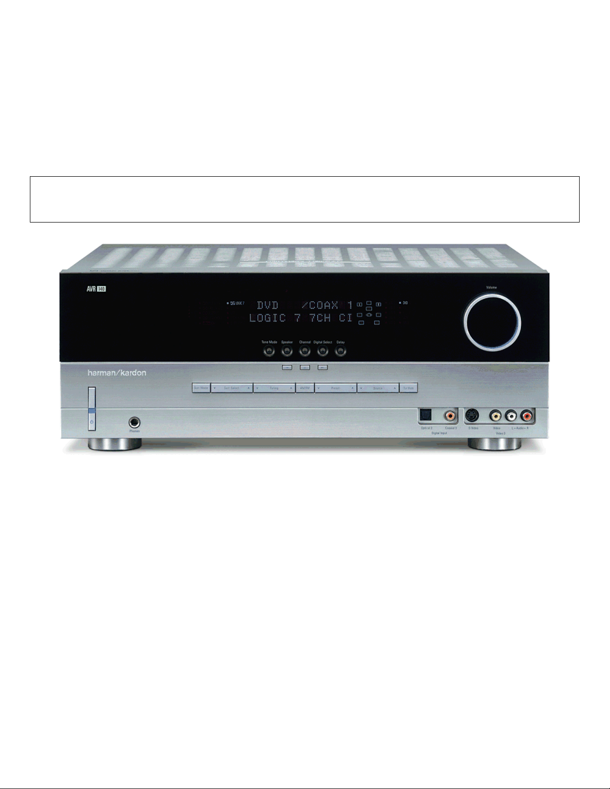
AVR140
6 X 40W 6.1 CHANNEL A/V RECEIVER
SERVICE MANUAL
ESD WARNING……………………………….2
LEAKAGE TESTING……………….…..…....3
BASIC SPECIFICATIONS…………………..4
PACKAGING…………………………….……5
FRONT PANEL CONTROLS………..…..…..6
REAR PANEL CONNECTIONS………….…8
REMOTE CONTROL FUNCTIONS……….10
CONNECTIONS………………………….…13
OPERATION………………………...………15
TROUBLESHOOTING GUIDE…...……..…21
PROCESSOR RESET……………….….…..21
DISASSEMBLY……………………………….22
harman/kardon, Inc.
250 Crossways Park Dr.
CONTENTS
UNIT EXPLODED VIEW…………..…….…..23
EXPLODED VIEW PARTS LIST……………24
AMP BIAS ADJUSTMENT……………….…25
BULLETIN HK2006-01…............................26
TECH TIP HK2003-01…...….….………..…27
BLOCK DIAGRAM…………………………..28
PCB DRAWINGS……………………………29
ELECTRICAL PARTS LIST………..………35
SEMICONDUCTOR PINOUTS…….………69
SCHEMATICS………………………………153
WIRING DIAGRAM………………………...160
Woodbury, New York 11797 Rev 0 3/2006
Page 2

AVR140 harman/kardon
2
Some semiconductor (solid state) devices can be damaged easily by static electricity. Such components commonly are called
Electrostatically Sensitive (ES) Devices. Examples of typical ES devices are integrated circuits and some field effect transistors and
semiconductor "chip" components.
The following techniques should be used to help reduce the incidence of component damage caused by static electricity.
1. Immediately before handling any semiconductor component or semiconductor-equipped assembly, drain off any electrostatic charge on
your body by touching a known earth ground. Alternatively, obtain and wear a commercially available discharging wrist strap device,
which should be removed for potential shock reasons prior to applying power to the unit under test.
2. After removing an electrical assembly equipped with ES devices, place the assembly on a conductive surface such as aluminum foil, to
prevent electrostatic charge build-up or exposure of the assembly.
3. Use only a grounded-tip soldering iron to solder or unsolder ES devices.
4. Use only an anti-static solder removal device. Some solder removal devices not classified as "anti-static" can generate electrical charges
sufficient to damage ES devices.
5. Do not use freon-propelled chemicals. These can generate electrical change sufficient to damage ES devices.
6. Do not remove a replacement ES device from its protective package until immediately before you are ready to install it. (Most replacement
ES devices are packaged with leads electrically shorted together by conductive foam, aluminum foil or comparable conductive material.)
7. Immediately before removing the protective material from the leads of a replacement ES device, touch the protective material to the
chassis or circuit assembly into which the device will be installed.
CAUTION :
8. Minimize bodily motions when handling unpackaged replacement ES devices. (Otherwise harmless motion such as the brushing together
or your clothes fabric or the lifting of your foot from a carpeted floor can generate static electricity sufficient to damage an ES devices.
Be sure no power is applied to the chassis or circuit, and observe all other safety precautions.
Each precaution inthis manualshould be followed during servicing.
Components identified with the IEC symbol in the parts list are special significance to safety. When replacing a component identified with
, use only the replacement parts designated, or parts with the same ratings or resistance, wattage, or voltage that are designated in the
parts list in this manual. Leakage-current or resistance measurements must be made to determine that exposed parts are acceptably
insulated from the supply circuit before retuming the product to the customer.
Page 3
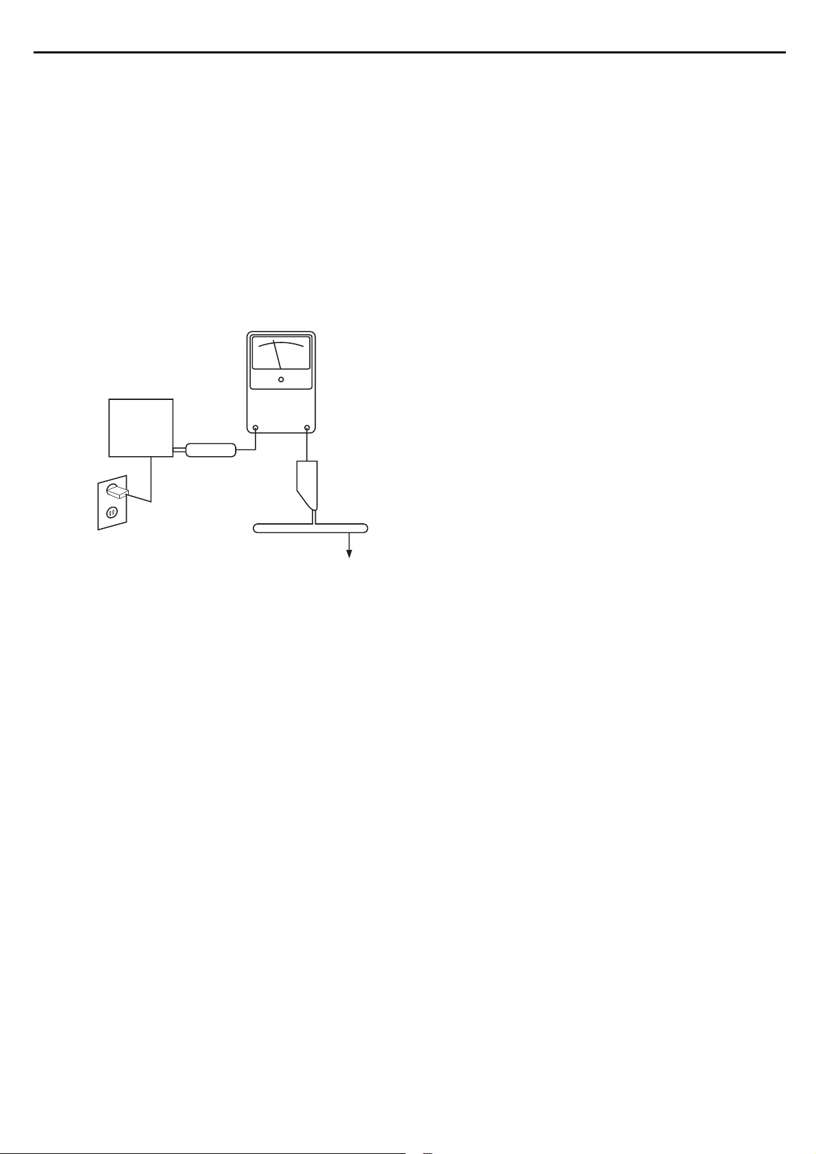
SAFETY PRECAUTIONS
The following check should be performed for the continued
protection of the customer and service technician.
LEAKAGE CURRENT CHECK
Measure leakage current to a known earth ground (water
pipe, conduit, etc.) by connecting a leakage current tester
between the earth ground and all exposed metal parts of the
appliance (input/output terminals, screwheads, metal
overlays, control shaft, etc.). Plug the AC line cord of the
appliance directly into a 120V AC 60Hz outlet and turn the
AC power switch on. Any current measured must not exceed
o.5mA.
ANY MEASUREMENTS NOT WITHIN THE LIMITS
OUTLINED ABOVE ARE INDICATIVE OF A
POTENTIAL SHOCK HAZARD AND MUST BE
CORRECTED BEFORE RETURNING THE APPLIANCE
TO THE CUSTOMER.
AVR140 harman/kardon
3
Reading should
not be above
0.5mA
Device
under
test
Leakage
current
tester
Test all
exposed metal
surfaces
Also test with
plug reversed
(Using AC adapter
plug as required)
Earth
ground
AC Leakage Test
Page 4

The
Bridge
T
M
AVR140 harman/kardon
4
AVR 140 TECHNICAL SPECIFICATIONS
AVR 140 TECHNICAL SPECIFICATIONS
Audio Section
Stereo Mode
Continuous Average Power (FTC)
50 Watts per channel, 20Hz–20kHz,
@ <0.07% THD, both channels driven into 8 ohms
Six-Channel Surround Modes
Power per Individual Channel
Front L&R channels:
40 Watts per channel
@ <0.07% THD, 20Hz–20kHz into 8 ohms
Center channel:
40 Watts @ <0.07% THD, 20Hz–20kHz into 8 ohms
Surround (L & R Side, Back) channels:
40 Watts per channel
@ <0.07% THD, 20Hz–20kHz into 8 ohms
Input Sensitivity/Impedance
Linear (High-Level) 200mV/47k ohms
Signal-to-Noise Ratio (IHF-A) 100dB
Surround System Adjacent Channel Separation
Pro Logic I/II 40dB
Dolby Digital (AC-3) 55dB
DTS 55dB
Frequency Response
@ 1W (+0dB, –3dB) 10Hz –130kHz
High Instantaneous
Current Capability (HCC) ±25 Amps
Transient Intermodulation
Distortion (TIM) Unmeasurable
Slew Rate 40V/µsec
FM Tuner Section
Frequency Range 87.5–108.0MHz
Usable Sensitivity IHF 1.3µV/13.2dBf
Signal-to-Noise Ratio Mono/Stereo 70/68dB
Distortion Mono/Stereo 0.2/0.3%
Stereo Separation 40dB @ 1kHz
Selectivity ±400kHz, 70dB
Image Rejection 80dB
IF Rejection 90dB
AM Tuner Section
Frequency Range 520–1720kHz
Signal-to-Noise Ratio 45dB
Usable Sensitivity Loop 500µV
Distortion 1kHz, 50% Mod 0.8%
Selectivity ±10kHz, 30dB
Video Section
Television Format NTSC
Input Level/Impedance 1Vp-p/75 ohms
Output Level/Impedance 1Vp-p/75 ohms
Video Frequency Response
(Composite and S-Video) 10Hz–8MHz (–3dB)
Video Frequency Response
(Component Video) 10Hz–50MHz (–3dB)
General
Power Requirement AC 120V/60Hz
Power Consumption 65W idle, 540W maximum
(6 channels driven)
Dimensions (Product) (Shipping)
Width 17.3 inches (440mm) 21.5 inches (545mm)
Height 6.6 inches (168mm) 9.9 inches (251mm)
Depth 15 inches (382mm) 17.9 inches (455mm)
(Product) (Shipping)
Weight 24.4 lb (11.1kg) 29.3 lb (13.3kg)
Depth measurement includes knobs, buttons and terminal connections.
Height measurement includes feet and chassis.
All features and specifications are subject to change without notice.
Harman Kardon, Power for the Digital Revolution, The Bridge, and Logic 7 are registered trademarks
of Harman International Industries, Incorporated.
*Manufactured under license from Dolby Laboratories. “Dolby,” “Pro Logic” and the Double-D symbol
are trademarks of Dolby Laboratories.
DTS, DTS Surround, DTS-ES and DTS Neo:6 are registered trademarks of Digital Theater Systems, Inc.
VMAx is a registered trademark of Harman International Industries, Incorporated, and is an
implementation of Cooper Bauck Transaural Stereo under patent license.
Cirrus is a registered trademark of Cirrus Logic, Inc.
SACD is a trademark of Sony Electronics, Inc.
Apple and iPod are registered trademarks of Apple Computer, Inc.
Please register your product on our Web site at www.harmankardon.com. Note: You’ll need your serial number.
At the same time you can choose to be notified about our new products and/or special promotions.
50 TECHNICAL SPECIFICATIONS
Page 5

AVR140 harman/kardon
5
0-Hmrsqtbshnml`mt`k`rr&x,@bbdrrnqhdr 1-O`bj`fdCq`vhmf
0
ONKXA@F
3
A@SSDQX@RR&X
QDLNBNM
SQ@MRLHSSDQ@RR&X
0/
BNUDQ@RR&X
00
HL@FDAQNBGTQDR
1
B@QCV@QQ@MSX
4
L@MT@KHMRSQTBSHNM
76
RGDDSFTHCD
MN CDRBQHOSHNM O@QSRMN- P+sx
0
B@QCV@QQ@MSX
1
2
@LKNNO@MSDMM@
3
A@SSDQX
4
HMRSQTBSHNML@MT@K
5
EL0ONK@MS'TK(
6
QDLNBNMSQ@MRLHSSDQ@RR&X
RGDDSFTHCD'PTHBJRS@QSFTHCD(
7
RS@OKD8
BNUDQ@RR&X0/ BFQ@UQ02/Y@ 0
0
BNUDQ@
1
BNUDQA
2
RGDDS+EQNMSBNUDQ
3
O@C+BNUDQ
4
A@F+ONKX
HL@FDAQNBGTQDR00 GPD0@162Y 0
2
@LKNNO@MSDMM@@RR&X
5
EL0ONKD@MS'TK(
8
RS@OKD
BOA0/50XONKXA@F
BPD0@061W 0
BR@0@/16Y
G@A@@@L0-4UGJ
BPW0@0/14Y
BR@0@/08Y 0
G@QS@UQ03/
BPD0@147Y
JOK/8/4
BFQ0@220L6G32
BFQ0@221L6G32
BPD0@108Y
BOR0@565
BOA0@065Y
1
RMNVO@C'K(
RDS
AVR140
3
0
0
2
0
0
0
0
2
0
00
0
0
0
L@MT@K@RR&X
0
Access. Package
RMNV+O@C'K(
1
AVR140
3
RDS @UQ03/RDS 0
ANW+NTSB@QSNM
4
@UQ03/
Access. Package
L@MT@K@RR&X
0
RMNVO@C'Q(
2
ANW+NTSB@QSNM
4
CDRBQHOSHNMMN
BPW@UQ03/
BOR4@453
BOR4@454RMNV+O@C'Q(20
AVR 140
BOF0@686Y00
P+sxO@QSRMN-
0
Page 6
DIGITAL LOGIC 7
VID 1
DVD
CD
FMAM
TAPE
6 8 CH
VID 2
VID 3
PRO LOGIC
3 STEREO DSP
5 7 CH. STEREO
SURR. OFF
1
2
6
7
#
Ú
(
*
Û
8
)
!
@
)
&
%
3
4
˜
5
9
$
^
Ò
Ó
AVR 140
ˆ
Ù
Ô
ı
AVR140 harman/kardon
6
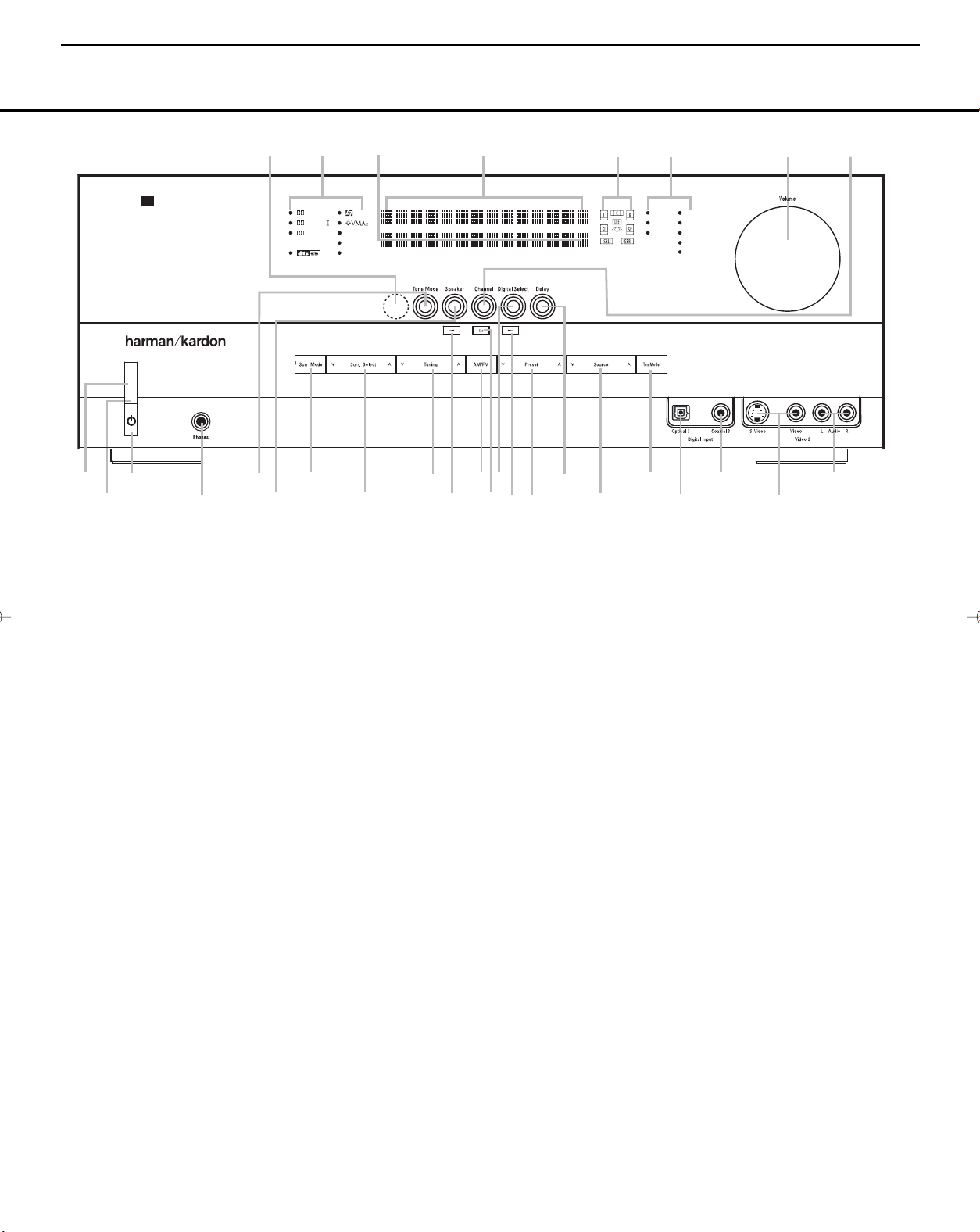
FRONT-PANEL CONTROLS
FRONT-PANEL CONTROLS
NOTE: To make it easier to follow the instructions that refer to this illustration, a larger copy may be downloaded from the Product Support section for this product
at www.harmankardon.com.
1 Main Power Switch
2 Power Indicator
3 Standby/On Switch
4 Headphone Jack
5 Tone Mode
6 Speaker Selector
7 Surround Mode Group Selector
8 Surround Mode Selector
9 Tuning Selector
‹/›
)
Buttons
1 Main Power Switch: Press this button to apply
power to the AVR 140. When the switch is pressed
in, the unit is in a Standby mode, as indicated by the
amber LED
2 above the Standby/On Switch 3.
This button MUST be pressed in to operate the unit.
To turn the unit off and prevent the use of the remote
control, this switch should be pressed until it pops
out from the front panel and the word “OFF” is seen
at the top of the switch.
NOTE: This switch is normally left in the “ON” position.
2 Power Indicator: This LED lights amber when the
unit is in the Standby mode to signal that the AVR is
ready to be turned on. When the unit is in operation,
the indicator is blue.
3 Standby/On Switch: When the Main Power
1
Switch
is “ON,” press this button to turn on the
AVR 140; press it again to turn the unit off. The
Indicator
3
turns blue when the unit is on.
Power
! Tuner Band Selector
@ Set Button
# Digital Input Selector
$ Preset Station Selector
% Delay Adjust Selector
^ Input Source Selector
& Tuner Mode Selector
* Optical 3 Digital Audio Input
( Coaxial 3 Digital Audio Input
Ó Video 3 Video Input Jacks
4 Headphone Jack: This jack may be used to listen
to the AVR 140’s output through a pair of headphones.
The speakers will automatically be turned off when the
headphone jack is in use.
5 Tone Mode: This button controls the tone mode
settings, enabling adjustment of the bass and treble
boost/cut. You may also use it to take the tone controls out of the signal path completely for “flat”
response.The first press of the button displays a
TONE IN message in the Lower Display Line
ı and in the on-screen display. To take the controls
out of the signal path, press either of the
‹
›
‹
›
/
Buttons ) until the display reads TONE OUT.
To change the bass or treble settings, make sure that
TONE IN appears in the Lower Display Line ı
‹
›
‹
or press either of the
›
/
Buttons ) until it does.
Press the Tone Mode Button 5 until the desired
option of
TREBLE MODE or BASS MODE
appears in the Lower Display Line ı and in the
‹
›
‹
on-screen display and then press either of the
›
/
Ô Video 3 Audio Input Jacks
Channel Adjust Selector
Ò Volume Control
Ú Input Indicators
Û Speaker/Channel Input Indicators
Ù Upper Display Line
ı Lower Display Line
ˆ Surround Mode Indicators
˜ Remote Sensor Window
Both treble and bass contours may be boosted or
cut by up to + or –10dB in increments of 2dB. See
pages 17 and 25 for more information on the tone
controls.
NOTE: The AVR 140 is not equipped with a traditional
Balance control. When listening to two-channel materials, if you wish to adjust the stereo image, you may
use the
Channel Adjust Selector to increase or
decrease the level of the left front channel by up to +
or –10dB, and then to decrease or increase the right
front channel by the corresponding amount. However,
when listening to surround materials and most twochannel materials, it is recommended that you leave
these settings at the results obtained during the configuration process described on pages 15 through 24.
6 Speaker Selector: Press this button to begin
the process of configuring the unit to match the type
of speakers used in your listening room. (See pages
20–22 for more information on speaker setup and
configuration.)
Buttons ) to enter the desired boost or cut setting.
FRONT-PANEL CONTROLS 55
Page 7

AVR140 harman/kardon
7
FRONT-PANEL CONTROLS
7 Surround Mode Group Selector: Press this but-
ton to select the top-level group of surround modes.
Each press of the button will select the current or last
used mode in each of the surround mode groups
(e.g., Dolby, DTS, DTS Neo:6, Logic 7, DSP, Stereo).
When the button is pressed so that the name of the
surround mode group appears in the on-screen display and in the
Surround Mode Selector 8 to cycle through the
individual modes available. For example, press this
button to select Dolby modes, and then press the
Surround Mode Selector 8 to choose from the
various Dolby mode options.
8 Surround Mode Selector: Press this button
to select from among the available surround mode
options for the mode group selected. The specific
modes will vary based on the number of speakers
available, the mode group and if the input source is
digital or analog. For example, press the
Mode Group Selector
grouping such as Dolby or Logic 7, and then press
this button to see the specific mode choices available.
Note that the digital surround modes, such as Dolby
Digital and DTS, may not be accessed unless that type
of source signal is present, such as when a DVD movie
or television signal programmed in Dolby Digital or DTS
surround sound is playing. For more information on surround mode selection, see pages 18 and 26.
9 Tuning Selector: Press the left side of the button
to tune lower-frequency stations and the right side of
the button to tune higher-frequency stations. When the
tuner is in the Manual mode, each tap will increase or
decrease the frequency by one increment. When the
tuner receives a strong enough signal for adequate
reception,
on-screen display and the
When the tuner is the Auto mode, press the button
once, and the tuner will scan for a station with acceptable signal strength. When the next station with a
strong signal is tuned the scan will stop and the
on-screen display and
will indicate AUTO TUNED. When an FM
Stereo station is tuned, the display will read
AUTO ST TUNED.
To switch back and forth between the Auto and
Manual tuning modes, press the
Selector
) ‹/› Buttons: When configuring the AVR 140’s
settings, use these buttons to select from the available
choices
! Tuner Band Selector: Press this button to turn
the AVR on and to select the Tuner as the input. Press
it again to switch between the AM and FM frequency
bands. (See page 30 for more information on the tuner.)
Lower Display Line ı, press the
Surround
7 to select a main mode
MANUAL TUNED will appear in the
Lower Display Line ı.
Lower Display Line ı
Tuner Mode
&.
.
@ Set Button: When making choices during the
setup and configuration process, press this button
to enter the desired setting into the AVR 140’s memory.
# Digital Input Selector: Press this button to
select one of the digital audio inputs or the analog
audio input for any source. (See pages 26–30 for
more information on digital audio.)
$ Preset Stations Selector: Press this button to
scroll up or down through the list of stations that have
been entered into the preset memory. (See page 30
for more information on tuner presets.)
% Delay Adjust Selector: Press this button to
begin the steps required to enter delay settings. (See
pages 22–23 for more information on delay times.)
^ Input Source Selector: Press this button to
change the input by scrolling up or down through the
list of
Input Indicators Ú.
& Tuner Mode Selector: Press this button to select
Auto or Manual tuning.When the button is pressed so
that the
AUTO appears in the Lower Display Line
ı, the tuner will search for the next station with an
acceptable signal when the
is pressed. When the button is pressed so that
MANUAL appears in the Lower Display Line ı,
each press of the
increase the frequency.This button may also be used to
switch between Stereo and Mono modes for FM radio
reception. When weak reception is encountered, press
the button so that
Display Line
switch to Mono reception. Press it again to switch back
to Stereo mode. (See page 30 for more information on
using the tuner.)
* Optical 3 Digital Audio Input: Connect the optical
digital audio output of an audio or video product to this
jack. When the input is not in use, the built-in shutter will
close to avoid dust contamination that might degrade
future performance.
( Coaxial 3 Digital Audio Input: This jack is used
for connection to the output of portable audio devices,
video game consoles or other products that have a
coax digital audio jack.
Ó Video 3 Video Input Jacks: These jacks may
be used for temporary connection to the composite or
S-video output of video games, camcorders or other
portable video products.You may make a connection
to either jack at any time, but not to both simultaneously.
Ô Video 3 Audio Input Jacks: These audio jacks
may be used for temporary connection to video
games or portable audio/video products such as
camcorders and portable audio players.
ı and on the on-screen display to
Tuning Selector 9u
Tuning Selector 9u will
MANUAL appears in the Lower
Channel Adjust Selector: Press this button to
begin the process of trimming the channel output levels using an external audio source. (For more information on output level trim adjustment, see page 23.)
Ò Volume Control: Turn this knob clockwise to
increase the volume, counterclockwise to decrease the
volume. If the AVR 140 is muted, adjusting the
Volume Control Òb will automatically release the
unit from the silenced condition.
Ú Input Indicators: The current selected source will
appear as one of these indicators. Note that when the
unit is turned on, the entire list of available modes will
light briefly, and then revert to normal operation with
only the active mode indicator illuminated.
Û Speaker/Channel Input Indicators: These indi-
cators are multipurpose, indicating both the speaker
type selected for each channel and the incoming datasignal configuration. The left, center, right, right surround
and left surround speaker indicators are composed of
three boxes, while the subwoofer is a single box. The
center box lights when a “small” speaker is selected,
and the two outer boxes light when “large” speakers are
selected. When none of the boxes are lit for the center,
surround or subwoofer channels, no speaker has been
assigned that position. (See page 20 for more information on configuring speakers.)
The letters inside each box display the active input
channels. For standard analog sources, only the L and R
will light, indicating a stereo input. For a digital source,
the indicators will light to display the channels being
received at the digital input. When the letters flash, the
digital input has been interrupted. (See page 29 for
more information on the Channel Indicators.)
Ù Upper Display Line: Depending on the unit’s sta-
tus, a variety of messages will appear here. In normal
operation, this line will show current input source and
which analog or digital input is in use.When the tuner is
the input, this line will identify the station as AM or FM
and show the frequency and preset number, if any.
ı Lower Display Line: Depending on the unit’s sta-
tus, a variety of messages will appear here. In normal
operation, the current surround mode will show here.
ˆ Surround Mode Indicators: The current selected
surround mode will appear as one of these indicators.
Note that when the unit is turned on, the entire list of
available modes will light briefly, and then revert to
normal operation with only the active mode indicator
illuminated.
˜ Remote Sensor Window: The sensor behind
this window receives infrared signals from the remote
control. Aim the remote at this area and do not block
or cover it.
6 FRONT-PANEL CONTROLS
Page 8
•
∞
¶
⁄
fi
ª
¡
£
‹
°
b
d
g
j
i
a
™
¢
§
‚
¤
›
fl
‡
·
c
e
f
h
k
32
3
1
1
40140
(
100W, 1A MAX)(100W, 1A MAX)
(50W, 0.5A MAX)(50W, 0.5A MAX)
T
he Bridge
The
Bridge
TM
AVR140 harman/kardon
8
REAR-PANEL CONNECTIONS
NOTE: To make it easier to follow the instructions that refer to this illustration, a larger copy may be downloaded from the Product Support section for this product
at www.harmankardon.com.
¡ FM Antenna Jack
™ CD Audio Inputs
£ Tape Outputs
¢ Tape Inputs
∞ Subwoofer Output
§ Front Speaker Outputs
¶ Surround Back Speaker Outputs
• Surround Speaker Outputs
ª Center Speaker Outputs
‚ Component Video Monitor Outputs
⁄ Component Video 1 Inputs
NOTE: To assist in making the correct connections
for multichannel input, output and speaker connections, all connection jacks and terminals are colorcoded in conformance with the CEA standards as
follows:
Front Left: White
¡ FM Antenna Jack: Connect the supplied indoor
(or an optional external) FM antenna to this terminal.
™ CD Audio Inputs: Connect these jacks to the
analog audio outputs of a compact disc player or CD
changer.
£
Tape Outputs: Connect these jacks to the
RECORD/INPUT
¢ Tape Inputs:
PLAY/OUT
jacks of an audio recorder.
Connect these jacks to the
jacks of an audio recorder.
¤ Component Video 2 Inputs
‹ AC Power Cord
› Switched AC Accessory Outlet
fi Unswitched AC Accessory Outlet
fl Optical Digital Audio Output
‡ Coaxial Digital Audio Output
° S-Video Monitor Output
· Coaxial Digital Audio Inputs
a DVD S-Video Input
b DMP Connector
c Video 1 S-Video Input
Front Right: Red
Center: Green
Surround Left: Blue
Surround Right: Gray
Surround Back Left: Brown
Surround Back Right: Tan
∞ Subwoofer Output: Connect this jack to the line-
level input of a powered subwoofer. If an external subwoofer amplifier is used, connect this jack to the subwoofer amplifier input.
§ Front Speaker Outputs: Connect these outputs
to the matching + or – terminals on your left and right
speakers.When making speaker connections always
make certain to maintain correct polarity by connecting
the color-coded (white for front left and red for front
right) (+) terminals on the AVR 140 to the red (+)
d Optical Digital Audio Inputs
e Video 1 S-Video Output
f Video 2 S-Video Input
g 6/8-Channel Direct Inputs
h Video Monitor Output
i DVD Audio/Video Inputs
j Video 1 Audio/Video Inputs
k Video 1 Audio/Video Outputs
U Video 2 Audio/Video Inputs
V AM Antenna Terminals
Subwoofer: Purple
Coaxial Digital Audio: Orange
Composite Video: Yellow
Component Video “Y”: Green
Component Video “Pr”: Red
Component Video “Pb”: Blue
terminals on the speakers and the black (–) terminals
on the AVR 140 to the black (–) terminals on the
speakers. See page 12 for more information on
speaker polarity.
¶ Surround Back Speaker Outputs: These
speaker terminals are normally used to power the surround back speaker in a 6.1-channel system. Connect
these outputs to the matching + and – terminals on
your surround back channel speaker. In conformance
with the CEA color-code specification, the brown ter-
REAR-PANEL CONNECTIONS 7
Page 9

The
Bridge
TM
The
Bridge
T
M
AVR140 harman/kardon
9
REAR-PANEL CONNECTIONS
REAR-PANEL CONNECTIONS
minal is the positive, or “+,” terminal that should be
connected to the red (+) terminal on the Surround
Back speaker with older color-coding. Connect the
black (–) terminal on the AVR to the matching black
negative (–) terminal on the surround back speaker.
(See page 12 for more information on speaker
polarity.)
• Surround Speaker Outputs: Connect these out-
puts to the matching + and – terminals on your surround channel speakers. In conformance with the CEA
color-code specification, the blue terminal is the positive, or “+,” terminal that should be connected to the
red (+) terminal on the Surround Left speaker with
older color-coding, while the gray terminal should be
connected to the red (+) terminal on the Surround
Right speaker with the older color-coding. Connect the
black (–) terminal on the AVR to the matching black
negative (–) terminals for each surround speaker. (See
page 12 for more information on speaker polarity.)
ª Center Speaker Outputs: Connect these outputs
to the matching + and – terminals on your center
channel speaker. In conformance with the CEA
color-code specification, the green terminal is the
positive, or “+,” terminal that should be connected to
the red (+) terminal on speakers with the older colorcoding. Connect the black (–) terminal on the AVR to
the black (–) terminal on your speaker. (See page 12
for more information on speaker polarity.)
‚ Component Video Monitor Outputs: Connect
these outputs to the component video inputs of a
video projector or monitor. When a source connected
to one of the
Component Video Inputs ⁄¤ is
selected, the signal will be sent to these jacks.
⁄ Component Video 1 Inputs: Connect the
Y/Pr/Pb component video outputs of a DVD player,
HDTV set-top converter, satellite receiver or other
video source device with component video outputs to
these jacks.
¤ Component Video 2 Inputs: Connect the
Y/Pr/Pb component video outputs of a DVD player,
HDTV set-top converter, satellite receiver or other
video source device with component video outputs to
these jacks.
See page 17 for information on assigning the
Component Video 1 and 2 Inputs ⁄¤ to the
appropriate source inputs.
‹ AC Power Cord: Connect the AC power cord to a
non-switched AC wall outlet.
› Switched AC Accessory Outlet: These outlets
may be used to power any device you wish to have
turned on when the AVR 140 is turned on.
fi Unswitched AC Accessory Outlet: This outlet
may be used to power any AC device. The power will
remain on at this outlet regardless of whether the
AVR 140 is on or off.
NOTE: The total power consumption of all devices
connected to the accessory outlets should not exceed
100 watts.
fl Optical Digital Audio Output: Connect this jack
to the optical digital input connector on a CD-R/RW,
MiniDisc or other digital recorder.
‡ Coaxial Digital Audio Output: Connect this jack
to the coaxial digital input of a CD-R/RW, MiniDisc or
other digital recorder.
° S-Video Monitor Output: If any of the input
sources used in your system have S-video connections to the AVR, connect this jack to the S-video input
on your television, projector or other video display.
· Coaxial Digital Audio Inputs: Connect the coax
digital output from a DVD player, HDTV receiver,
player
or CD player to these jacks.The signal may be a
LD
Dolby Digital signal, DTS signal or a standard PCM digital
source. Do not connect the RF digital output of an LD
player to these jacks.
a DVD S-Video Input: Connect the S-video output of
a DVD player or other video source to this jack.
b Digital Media Player (DMP) Connector:
With the AVR 140 turned off, connect one end of the
optional Harman Kardon to this proprietary
connector, and the other to your compatible Apple
iPod. When the Digital Media Player source is selected,
you may view your iPod’s control and navigation messages on your video display (if one is connected to
one of the
the
Video Monitor Outputs °h), and in
Upper and Lower Display Lines PQ. You
may navigate the iPod and select tracks for playback
using the
Button
⁄
› Buttons no, the Set
/¤/‹/
p and Transport Controls z on your
AVR remote. See page 30 for more information.
c Video 1 S-Video Input: If the product connected to
the
Video 1 Audio Inputs j has S-video capability,
connect this jack to the PLAY/OUT S-video jack on
that unit and then make certain that the
Monitor Output
° is connected as described
S-Video
above.
d Optical Digital Audio Inputs: Connect the optical
digital output from a DVD player, HDTV receiver, LD
player or CD
player to these jacks.The signal may be a
Dolby Digital signal, a DTS signal or a standard PCM
digital source.
e Video 1 S-Video Output: If the product connected
to the
Video 1 Audio/Video Outputs k has S-video
capability, connect this jack to the REC/IN S-video jack
on that unit.
f Video 2 S-Video Input: If the product connected
to the
Video 2 Audio/Video Inputs U has S-video
capability, connect this jack to the PLAY/OUT S-video
jack on that unit and then make certain that the
S-Video Monitor Output ° is connected as
described above.
g 6/8-Channel Direct Inputs: These jacks are
used for connection to source devices such as DVDAudio or SACD
™
players with discrete analog outputs.
Depending on the source device in use, all eight jacks
may be used, though in many cases only connections
to the front left/right, center, surround left/right and
LFE (subwoofer input) jacks will be used for standard
5.1 audio signals.
h Video Monitor Output: Connect this jack to the
composite video input of a TV monitor or video projector to view the on-screen menus and the output of a
standard video source.
i DVD Audio/Video Inputs: Connect the composite
video and L/R analog audio outputs of a DVD player or
other video source to these jacks.
j Video 1 Audio/Video Inputs: Connect the com-
posite video and L/R analog audio PLAY/OUT jacks of
a VCR or other video source to these jacks.
k Video 1 Audio/Video Outputs: Connect the
composite video and L/R analog audio REC/IN jacks
of a VCR or other video recording device such as a
DVD recorder or PVR to these jacks.
U Video 2 Audio/Video Inputs: Connect the com-
posite video and L/R analog audio PLAY/OUT jacks of
a cable television box or other video source to these
jacks.
VAM Antenna Terminals: Connect the AM loop
antenna supplied with the receiver to these terminals.
If an external AM antenna is used, make connections
to the
AM and GND terminals in accordance with
the instructions supplied with the antenna.
NOTE ON VIDEO CONNECTIONS: When connecting
a video source product such as a VCR, DVD player,
satellite receiver, cable set-top box, personal video
recorder or video game to the AVR 140, you may
use either a composite or S-video connection, but
not both.
8 REAR-PANEL CONNECTIONS
8 REAR-PANEL CONNECTIONS
Page 10
The
Bridge
TM
s
a
bc
d
e
f
g
h
j
n
n
p
o
o
q
r
t
v
`
3
2
30
29
28
36
37
38
39
z
x
3
5
P
OWER
MUTE
AVR
DVD
AM/FM
CD
TAPE
VID 2
VCR
TV
CBL/SAT
6/8 CH
DMP
VID 1
VID 3
O
FF
O
N
SLEEP
T/V
SURR.
CH.
VOL.
G
U
I
D
E
C
H
.
E
X
I
T
D
I
G
I
T
A
L
M
E
N
U
S
P
K
R
P
R
E
V
.
C
H
.
D
E
L
A
Y
SET
1
2
3
4
7
6
5
9
0
TUN-M
MEM
M2
M3
M4
D.SKIP
M1
DIRECT
OSD
TUNING
DOLBY SUR
DTS SUR
DTS NEO:6
STEREO
LOGIC 7
SKIP
UP
DOWN
PRESET
CLEAR
TEST
NIGHT
11
44
00
8
l
u
DIM
i
k
m
34
33
w
y
41
4
0
3
1
42
®
The
Bridge
TM
10
AVR140 harman/kardon
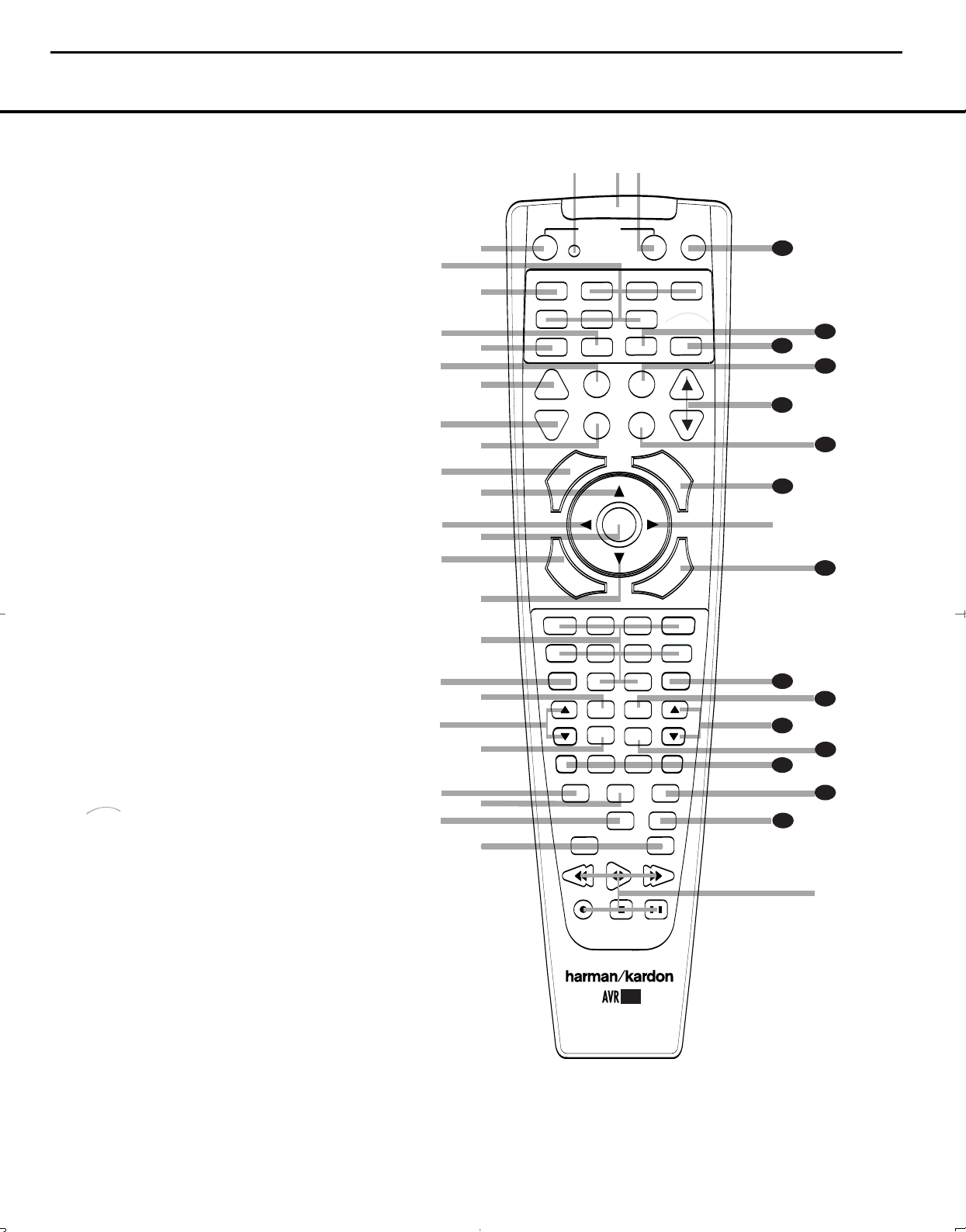
REMOTE CONTROL FUNCTIONS
a Power Off Button
b IR Transmitter Window
c Program Indicator
d Power On Button
e Input Selectors
f AVR Selector
g AM/FM Tuner Select
h Dim Button
i Test Button
j Sleep Button
k DSP Surround Mode Selector
l Night Mode
m Channel Select Button
n
⁄/¤
Buttons
o
‹/›
Buttons
p Set Button
q Digital Select
r Numeric Keys
s Tuner Mode
t Direct Button
u Tuning Up/Down
v OSD Button
w Dolby Mode Selector
x DTS Digital Mode Selector
y Logic 7 Mode Select Button
z Skip Up/Down Buttons
` Transport Controls
R Stereo Mode Select Button
S DTS Neo:6 Mode Select
T
U
V
W
X
Y
Z
a
b
c
d
e
f
Macro Buttons
Disc Skip Button
Preset Up/Down
Clear Button
Memory Button
Delay/Prev. Ch.
Speaker Select
Spare Button
Volume Up/Down
TV/Video Selector
DMP Selector
6-Channel/8-Channel Direct Input
Mute
NOTES:
• The function names shown here are each button’s
feature when used with the AVR 140. Most buttons
have additional functions when used with other
devices. See pages 37–38 for a list of these
functions.
• To make it easier to follow the instructions that refer
to this illustration, a larger copy may be downloaded from the Product Support section for this
product at www.harmankardon.com.
REMOTE CONTROL FUNCTIONS 9
Page 11
AVR140 harman/kardon
11
REMOTE CONTROL FUNCTIONS
IMPORTANT NOTE: The AVR 140’s remote may
be programmed to control up to seven devices,
including
the AVR 140. Before using the remote, it is
important to
Button
remember to press the Input Selector
e that corresponds to the unit you wish to
operate. In addition, the AVR 140’s remote is shipped
from the factory to operate the AVR 140 and most
Harman Kardon CD or DVD players and cassette
decks.The remote is also capable of operating a wide
variety of other products using the control codes that
are part of the remote. Before using the remote with
other products, follow the instructions on page 34
to program the proper codes for the products in
your system.
It is also important to remember that many of the buttons on the remote take on different functions, depending on the product selected using the Device Control
Selectors.The descriptions shown here primarily detail
the functions of the remote when it is used to operate
the AVR 140. (See pages 35–38 for information about
alternate functions for the remote’s buttons.)
a Power Off Button: Press this button to place the
AVR 140 or a selected device in the Standby mode.
Note that this will turn off the main room functions, but
if the Multiroom system is activated, it will continue
to function.
b IR Transmitter Window: Point this window
towards the AVR 140 when pressing buttons on the
remote to make certain that infrared commands are
properly received.
c Program Indicator: This three-color indicator is
used to guide you through the process of programming the remote. (See page 34 for information on
programming the remote.)
d Power On Button: Press this button to turn on
the power to a device selected by pressing one of the
Input Selectors e.
e Input Selectors: Pressing one of these buttons
will perform three actions at the same time. First, if the
AVR 140 is not turned on, this will power up the unit.
Next, it will select the source shown on the button as
the input to the AVR 140. Finally, it will change the
remote control so that it controls the device selected.
After pressing one of these buttons you must press
the
AVR Selector Button f again to operate the
AVR 140’s functions with the remote.
f AVR Selector: Pressing this button will switch the
remote so that it will operate the AVR 140’s functions. If
the AVR 140 is in the Standby mode, it will also turn the
AVR 140 on.
g AM/FM Tuner Select: Press this button to select
the AVR 140’s tuner as the listening choice. Pressing
this button when the tuner is already in use will select
between the AM and FM bands.
h Dim Button: Press this button to activate the
Dimmer function, which reduces the brightness of the
front panel display, or turns it off entirely. The first press
of the button shows the default state, which is full brightness by indicating
Display Line
VFD FULL in the Lower
ı. Press the button again within five
seconds to reduce the brightness by 50%, as indicated
by
VFD HALF showing in the Lower Display Line
ı. Press the button again within five seconds and the
main display will go completely dark. Note that this setting is temporary, in that regardless of any changes, the
display will always return to full brightness when the AVR
is turned on. In addition, the
Power Indicator 2 will
always remain at full brightness regardless of the setting.
This is to remind you that the AVR is still turned on.
i Test Button: Press this button to begin the
sequence used to calibrate the AVR 140’s output levels.
(See pages 23 and 31 for more information on calibrating the AVR 140.)
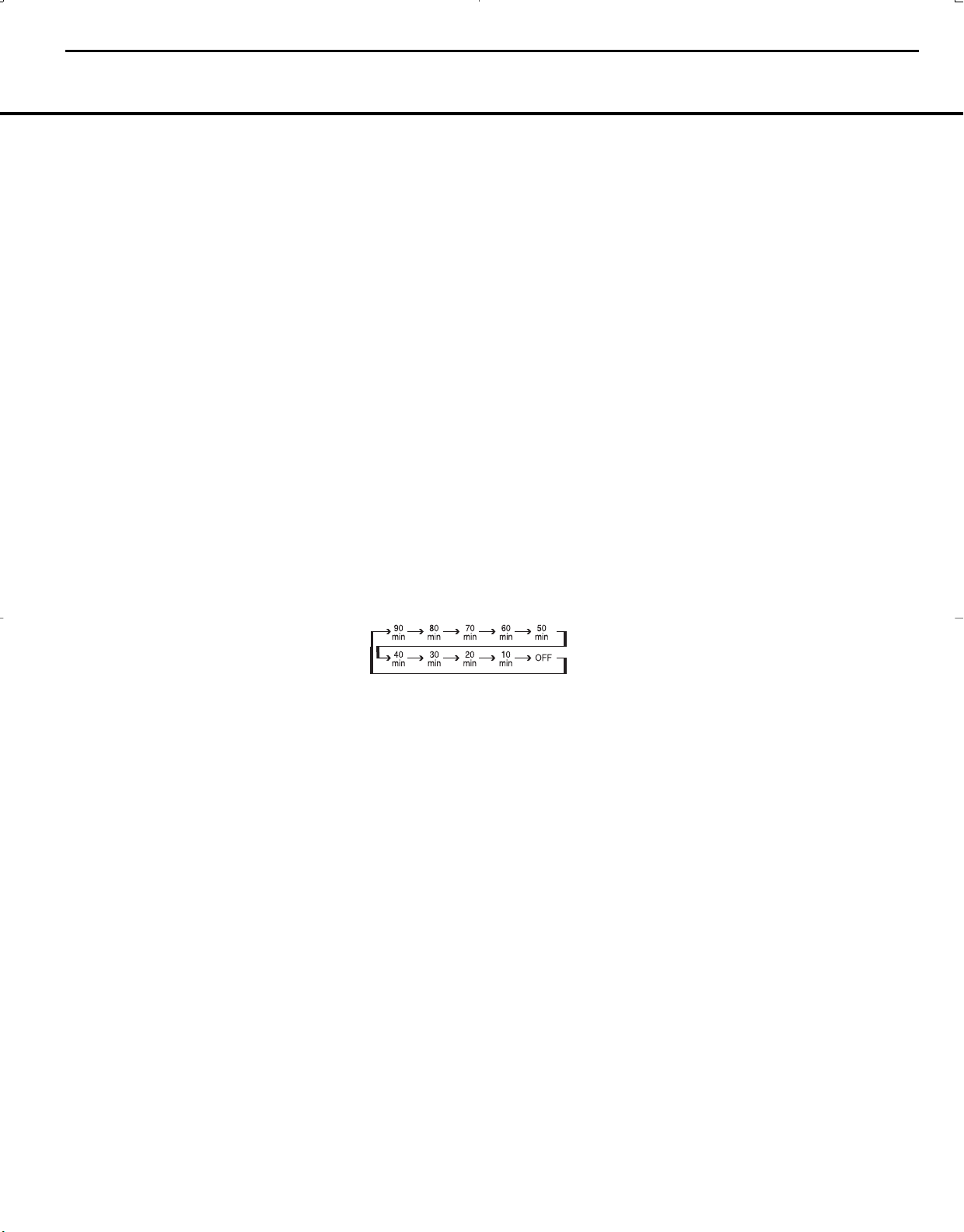
j Sleep Button: Press this button to place the unit
in the Sleep mode.After the time shown in the display,
the AVR 140 will automatically go into the Standby
mode. Each press of the button changes the time until
turn-off in the following order:
See page 25 for more information on the Sleep
Function. This button is also used to change channels
on your TV when the TV is selected.
When the AVR 140 remote is being programmed with
the codes to operate another device, this button is also
used in the “Auto Search” process. (See page 34 for
more information on programming the remote.)
k DSP Surround Mode Selector: Press this but-
ton to cycle through the DSP, VMAx and Stereo surround modes such as Hall, Theater, VMAx Near and
Far, and Surround Off. This button is also used to tune
channels when the TV is selected using the device
Input Selector e. When the AVR 140 remote is
being programmed with the codes of another device,
this button is also used in the “Auto Search” process.
(See page 34 for more information on programming
the remote.)
l Night Mode: Press this button to activate the
Night mode.This mode is available in specially
encoded digital sources, and it preserves dialogue
(center channel) intelligibility at low volume levels.
m Channel Select Button: This button is used to
start the process of setting the AVR 140’s output levels to
an external source. Once this button is pressed, use the
⁄/¤
Buttons n
then press the Set Button p, followed by the
Buttons
n again, to change the level setting. (See
to select the channel being adjusted,
⁄/¤
pages 23 and 31 for more information.)
⁄/¤
n
Buttons: These multipurpose buttons are
used to change or scroll through items in the onscreen menus, make configuration settings such as
digital inputs or delay timing, or to select surround
modes.When changing a setting, first press the button
for the function or setting to be changed (e.g., press
the
DSP Surround Mode Selector k to select a
sound field mode or the
Digital Select Button q
to change a digital input) and then press one of these
buttons to scroll through the list of options or to
increase or decrease a setting. The sections in this
manual describing the individual features and functions
contain specific information on using these buttons
for each application.
‹/›
o
Buttons: These buttons are used to change
the menu selection or setting during some of the setup
procedures for the AVR 140.
p Set Button: This button is used to enter settings
into the AVR 140’s memory. It is also used in the
setup procedures for delay time, speaker configuration
and channel output level adjustment.
q Digital Select: Press this button to assign one
of the digital inputs
*(·d to a source. (See
pages 17 and 28 for more information on using
digital inputs.)
r Numeric Keys: These buttons serve as a 10-
button numeric keypad to enter tuner preset positions.
They are also used to select channel numbers when
TV, Cable or SAT has been selected on the remote, or
to select track numbers on a CD, DVD or LD player,
depending on how the remote has been programmed.
I Tuner Mode: Press this button when the tuner
is in use to select between automatic tuning and
manual tuning. When the button is pressed so that
MANUAL appears in the Lower Display Line ı,
pressing the
Tuning Buttons 9u will move the
frequency up or down in single-step increments.
When the FM band is in use, pressing this button when
a station’s signal is weak will change to monaural
reception. (See page 30 for more information.)
J Direct Button: Press this button when the tuner
is in use to start the sequence for direct entry of a station’s frequency. After pressing the button, simply
press the proper
Numeric Keys r to select a sta-
tion. (See page 30 for more information on the tuner.)
u Tuning Up/Down: When the tuner is in use, these
buttons will tune up or down through the selected frequency band. If the
Tuner Mode Button s& has
10 REMOTE CONTROL FUNCTIONS
Page 12

The
Bridge
TM
The
Bridge
T
M
The
Bridge
TM
The
Bridge
T
M
AVR140 harman/kardon
12
REMOTE CONTROL FUNCTIONS
been pressed so that AUTO appears in the onscreen display and
Lower Display Line ı, pressing
and holding either of the buttons for three seconds will
cause the tuner to seek the next station with acceptable
signal strength for quality reception. When
MANUAL
appears in the Lower Display Line ı, pressing these
buttons will tune stations in single-step increments. (See
page 30 for more information.)
v OSD Button: Press this button to activate the
On-Screen Display (OSD) system used to set up or
adjust the AVR 140’s parameters.
w Dolby Mode Selector: This button is used to
select from among the available Dolby Surround processing modes. Each press of this button will select
one of the Dolby Pro Logic II modes or Dolby 3
Stereo.When a Dolby Digital-encoded source is in
use, the Dolby Digital mode may also be selected.
(See page 27 for the available Dolby surround mode
options.)
x DTS Digital Mode Selector: When a DTS-
encoded digital source is selected, each press of this
button will scroll through the available DTS modes.The
specific choice of modes will vary according to whether
or not the source material contains DTS-ES 6.1
Discrete encoding. When a DTS source is not in use,
this button has no function. (See page 27 for the available DTS digital options.)
y Logic 7 Mode Select Button: Press this button
to select from among the available Logic 7 surround
modes. (See page 27 for the available Logic 7
options.)
z Skip Up/Down Buttons: These buttons do not
have a direct function with the AVR 140, but when
used with a compatibly programmed CD or DVD
changer they will change to the previous disc in the
changer or carousel.
` Transport Controls: These buttons do not have
any functions for the AVR 140, but they may be
programmed for the forward/reverse play operation
of a wide variety of CD or DVD players, and audio or
video cassette recorders. (See page 36 for more
information.)
R Stereo Mode Select Button: When the button
is pressed so that
the
Lower Display Line ı, with only the Surr Off
Surround Mode Indicator
SURROUND OFF appears in
ˆ lit, the AVR will operate in a bypass mode with true, fully analog, two-channel left/right stereo mode with no surround processing
or bass management, unlike other modes where digital processing is used. When the button is pressed so
that
SURROUND OFF appears in the Lower
Display Line
Surround Mode Indicators
ı, with both the DSP and Surr Off
ˆ lit, you may enjoy a
two-channel presentation of the sound along with the
benefits of bass management. Depending on whether
your system is configured for 5.1 or 6.1/7.1 channels, the next press of the button will cause either
5 CH STEREO or 7 CH STEREO to
appear, and the stereo signal will be routed to all five
(or seven) speaker channels. (See page 27 for more
information on stereo playback modes.)
S DTS Neo:6 Mode Select: Press this button to
select a DTS Neo:6 mode.These modes take a twochannel stereo- or matrix surround-encoded source
and create a full five-, six- or seven-channel sound
field. (See page 27 for the DTS Neo:6 options.)
T Macro Buttons: Press these buttons to store or
recall a “Macro”, which is a preprogrammed sequence
of commands stored in the remote. (See page 34 for
more information on storing and recalling macros.)
U Disc Skip Button: This button has no direct
function for the AVR 140 but is most often used to
change to the next disc in a CD or DVD player when
the remote is programmed for that type of device.
(See page 35 for more information on using the
remote with products other than the AVR 140.)
V Preset Up/Down: When the tuner is in use,
press these buttons to scroll through the stations
programmed into the AVR 140’s memory.When
some source devices, such as CD players, VCRs and
cassette decks, are selected using the device
Selectors
e, these buttons may function as
Input
Chapter Step or Track Advance.
W Clear Button: Press this button to clear incorrect
entries when using the remote to directly enter a radio
station’s frequency.
X Memory Button: Press this button to enter a radio
station into the AVR 140’s preset memory. First, tune
the desired station, and then press this button. Two
underline indicators will flash at the right side of the
Upper Display Line P, and within five seconds
press the
Numeric Keys r for the preset number
between 01 and 30 that you wish to assign to the
station. (See page 30 for more information.)
Y Delay/Prev Ch.: Press this button to begin
the process for setting the delay times used by the
AVR 140 when processing surround sound. After
pressing this button, the delay times are entered by
pressing the
⁄/¤
Set Button p and then using the
Buttons n to change the setting. Press the
Set Button p again to complete the process.
(See page 22 for more information.)
Z Speaker Select: Press this button to begin
the process of configuring the AVR 140’s bass management system for use with the type of speakers
used in your system. Once the button has been
pressed, use the
⁄/¤
Buttons n to select the
channel you wish to set up. Press the
Set Button
p and then select another channel to configure.
When all adjustments have been completed, press
the
Set Button p twice to exit the settings and
return to normal operation. (See page 20 for more
information.)
a Spare Button: This button has no direct function
for the AVR 140, but may be used by other devices.
b Volume Up/Down: Press these buttons to raise
or lower the system volume.
c TV/Video Selector: This button does not have a
direct function on the AVR 140, but when used with a
compatible VCR, DVD or satellite receiver, pressing this
button will switch between the output of the device
and the external video input.
d Digital Media Player (DMP)
Selector:
When Harman Kardon’s (optional) is connected to
Connector
Digital Media Player (DMP)
b and a compatible Apple®iPod®is
docked in , pressing this selector will select
the iPod as the audio source input device for the
AVR 140. In addition, if a video display is connected
to one of the
Video Monitor Outputs °h, the
iPod’s messages will appear on screen, and in the
Upper and Lower Display Lines PQ. The
⁄/¤
/‹/
› Buttons no, the Set Button
p and the Transport Controls ` may be used
to navigate the iPod and to operate many functions.
See page 30, and the manuals for The Bridge and
your iPod for more information.
e
6-Channel/8-Channel Direct Input: Press
this button to select the device connected to the
6/8-Channel Direct Inputs g.
(See page 25 for
more information.)
f Mute: Press this button to momentarily silence
the AVR 140 or TV set being controlled, depending on
which device has been selected. When the AVR 140
remote is being programmed to operate another device,
this button is pressed with the
Input Selector Button
e to begin the programming process. (See page
34 for more information on programming the remote.)
REMOTE CONTROL FUNCTIONS 11
Page 13

The
Bridge
T
M
The
Bridge
TM
The
Bridge
TM
AVR140 harman/kardon
13
INSTALLATION AND CONNECTIONS
System Installation
After unpacking the unit, locating it in a place with adequate ventilation and placing it on a solid surface capable
of supporting its weight, you will need to make the connections to your audio and video equipment.
IMPORTANT NOTE: For your personal safety and to
avoid possible damage to your equipment and speakers,
it is always a good practice to turn off and unplug the
AVR and ALL source equipment from the AC output
before making any audio or video system connections.
Audio Equipment Connections
We recommend that you use high-quality interconnect
cables when making connections to source equipment
and recorders to preserve the integrity of the signals.
1. Connect the analog outputs of a CD player to the
CD Audio Inputs ™.
NOTE: When the CD player has both fixed and vari-
able audio outputs, it is best to use the fixed output
unless you find that the input to the receiver is so low
that the sound is noisy, or so high that it is distorted.
2. Connect the analog Play/Out jacks of a cassette
deck, MD, CD-R or other audio recorder to the
Input Jacks
on the recorder to the
¢. Connect the analog Record/In jacks
Tape Output Jacks £ on the
AVR 140.
3. Connect the output of any digital sources such as
a CD or DVD changer or player, advanced video
game, a digital satellite receiver, HDTV tuner or digital
cable set-top box or the output of a compatible
computer sound card to the
Digital Audio Inputs
Optical and Coaxial
·d*(. We recommend
connecting the coaxial digital audio output of your
DVD player to the
Coax 1 Digital Audio Input ·,
since that digital input is assigned to the DVD source
by default.
4. Connect the
Outputs
Coaxial or Optical Digital Audio
fl‡ on the rear panel of the AVR 140 to the
matching digital input connections on a CD-R or MiniDisc
or other digital recorder.
5. Assemble the AM Loop Antenna supplied with the
unit so that the tabs at the bottom of the antenna loop
snap into the holes in the base. Connect it to the
Antenna Terminals
V.
Tape
AM
6. Connect the supplied FM antenna to the
ohm)
Connection ¡. The FM antenna may be an
FM (75-
external roof antenna, an inside powered or wire-lead
antenna or a connection from a cable TV system. If
the antenna or connection uses 300-ohm twin-lead
cable, you must use the 300-ohm-to-75-ohm adapter
supplied with the unit to make the connection.
7. With the AVR 140 turned off, connect the optional
Harman Kardon to
Player (DMP) Connector
®
Apple
iPod®may be docked in when you
Digital Media
b. Your compatible
wish to use it as your audio source device.Video
materials stored on the iPod are not able to be viewed
using the AVR.
8. Connect the front, center, surround and surround
back speaker outputs
§¶•ª to the respective
speakers.
To ensure that all the audio signals are carried to your
speakers without loss of clarity or resolution, we suggest that you use high-quality speaker cable. Many
brands of cable are available and the choice of cable
may be influenced by the distance between your
speakers and the receiver, the type of speakers you
use, personal preferences and other factors. Your dealer
or installer is a valuable resource to consult in selecting the proper cable.
Regardless of the brand of cable selected, we recommend that you use a cable constructed of
copper with a gauge of 14 or smaller.
multistrand
Remember that
in specifying cable, the lower the number, the thicker
the cable.
Cable with a gauge of 16 may be used for short runs
of less than 10 feet. We do not recommend that you
use cables with an AWG equivalent of 18 or higher,
due to the power loss and degradation in performance
that will occur.
Cables that are run inside walls should have the appropriate markings to indicate listing with UL, CSA or other
appropriate testing agency standards. Questions about
running cables inside walls should be referred to your
installer or a licensed electrician who is familiar with
the NEC and/or the applicable local building codes in
your area.
When connecting wires to the speakers, observe
proper polarity. Note that the positive (+) terminal of
each speaker connection may carry a specific color
code, as noted on page 7. However, many speakers
still use a red terminal for the positive (+) connection.
Connect the “negative” or “black” wire to the same terminal on both the receiver and the speaker.
NOTE: While most speaker manufacturers adhere to
an industry convention of using black terminals for
negative and red ones for positive, some may vary
from this configuration. To ensure proper phase and
optimal performance, consult the identification plate on
your speaker or the speaker’s manual to verify polarity.
If you do not know the polarity of your speaker, ask
your dealer for advice before proceeding, or consult
the speaker’s manufacturer.
We also recommend that the length of cable used
to connect speaker pairs be identical. For example,
use the same length piece of cable to connect the
front-left and front-right or surround-left and surround-right speakers, even if the speakers are a
different distance from the AVR 140.
Note that it is not possible to use the AVR 140 in a
7.1-channel configuration. Any source information
that the AVR receives or derives for the surround
back left and right channels, e.g. through the
Channel Direct Inputs
g or during 7-channel
6/8-
Stereo processing, is combined and outputted
to the single-channel
Outputs
¶.
Surround Back Speaker
9. Connections to a subwoofer are normally made via
a line-level audio connection from the
Output
∞ to the line-level input of a subwoofer with
Subwoofer
a built-in amplifier. When a passive subwoofer is used,
the connection first goes to a power amplifier, which
will be connected to one or more subwoofers. If you
are using a powered subwoofer that does not have
line-level input connections, follow the instructions furnished with the speaker for connection information.
10. If an external multichannel audio source with 5.1,
6.1, 7.1 outputs such as an external digital processor/decoder, DVD-Audio or SACD player is used, connect the outputs of that device to the
Direct Inputs
g.
6/8-Channel
Video Equipment Connections
Video equipment is connected in the same manner as
audio components.The use of high-quality interconnect
cables is recommended to preserve signal quality.
1. Connect a VCR’s, DVD recorder’s, personal video
recorder’s or other video source’s audio and video
Play/Out jacks to the
Video 1 Audio/Video and/or
S-Video Input Jacks LS on the rear panel. The
Audio and Video Record/In jacks on the recorder
should be connected to the
Video 1 Audio/Video
and/or S-Video Output Jacks NT on the AVR 140.
Although any video device may be connected to these
jacks, we recommend connecting your video recorder
so that you may take advantage of the fact that the
remote control is preprogrammed with video recorder
product codes for the Video 1 device.
2. Connect the analog audio and video outputs of a
satellite receiver, cable TV converter, television set or
any other video source to the
Video 2 Audio/Video
12 INSTALLATION AND CONNECTIONS
Page 14

AVR140 harman/kardon
14
INSTALLATION AND CONNECTIONS
and S-Video Input Jacks OU. Although any video
device may be connected to these jacks, we recommend connecting your cable TV converter or satellite
receiver so that you may take advantage of the fact
that the remote control is preprogrammed with the
product codes of these device types for the Video 2
device.
3. Connect the analog audio and video outputs of
a television or other video device to the front-panel
Video 3 Audio and Video Input Jacks ÓÔ.
Although any video or audio device may be connected
to these jacks, we recommend connecting your television so that you may take advantage of the fact that
the remote control is preprogrammed with television
product codes for the Video 3 device.
you are only using the television as a display device
(i.e., if you receive your television programs through
a cable box or satellite receiver), do not connect
the TV’s outputs to the
Input Jacks
AVR 140.
4. Connect the analog audio and video outputs of a
DVD or laser disc player to the
and S-Video Inputs
5. Connect the digital audio outputs of a DVD player,
satellite receiver, cable box or HDTV converter to the
appropriate
·d*(. Remember that the DVD source
defaults to the
sources default to their analog inputs, although any
source may be assigned to any digital audio input on
the receiver.
6. Connect the
Output
or S-video input of your television monitor or video
projector.
7. If both your video display monitor and at least one
video source device, such as a DVD player or HDTV
set-top box, is equipped with component video capability, then you may connect the component video outputs of the device to one of the two
Video Inputs
It is recommended that you connect a DVD player or
a digital recorder to the
⁄, as this input is assigned to the DVD, CD,Tuner
and Tape sources by default. Thus, whenever any of
these sources is selected, you may view the component video output of the device connected to the
Component Video 1 Inputs ⁄, enabling you
to view and listen to different sources.
Similarly, it is recommended that you connect any
audio/video device, such as a DVD-Audio or SACD
player or HDTV set-top box, to the Video 1,Video 2
Optical or Coaxial Digital Inputs
°h jacks on the receiver to the composite
Video 3 Audio and Video
ÓÔ, or to any other inputs on the
ai.
Coaxial 1 Digital Input ·. All other
Video and/or S-Video Monitor
⁄¤.
Component Video 1 Inputs
Important: If
DVD Audio/Video
Component
or Video 3 sources, or the 6-/8-channel direct inputs,
as the
Component Video 2 Inputs ¤ are assigned
to the Video 1, Video 2, Video 3 and 6-/8-channel
source audio inputs by default.
However, you may connect any component video
source to either set of component video inputs, as
they are assignable to any source.You will still need to
connect either the analog or digital audio outputs of
your component video device to the analog audio
inputs corresponding to the source (such as DVD
or Video 2 for a cable converter box), or to any
of the
Optical or Coaxial Digital audio Inputs
·d* (.
8. If the component video inputs are used, connect
the
Component Video Monitor Outputs ‚ to
the component video inputs of your TV, projector
or display device.
9. If you have a camcorder, video game or other
audio/video device that is connected to the AVR on a
temporary rather than permanent basis, connect the
audio, video and digital audio outputs of that device
to the
Front-Panel Inputs *(ÓÔ. A device
connected here is selected as the Video 3 input, and
the digital inputs must be assigned to the Video 3
input. (See page 17 for more information on input
configuration.)
VIDEO CONNECTION NOTES:
• When the component video jacks are used, the onscreen menus are not visible and you must switch
to the standard composite or S-video input on your
TV to view them.
• The AVR 140 will accept either standard composite,
S-video or Y/Pr/Pb component video signals.
However, it will not convert composite or S signals
to component video.
• When connecting a video source to the AVR 140,
you may use either composite, component or Svideo, but only one type of video may be connected
for each device.
• When more than one video format is used, it is
necessary to make a separate connection from
the AVR to your video display for each format.
For example, if both composite and component
sources are connected to the AVR 140, both the
Composite and Component Video Monitor
Outputs
‚h must be connected to the appro-
priate inputs on your video display.
AC Power Connections
This unit is equipped with two accessory AC outlets.
They may be used to power accessory devices, but
they should not be used with high-current-draw equip-
ment such as power amplifiers.The total power draw
to each outlet may not exceed 100 watts.
The
Switched AC Accessory Outlet › will receive
power only when the unit is on. This is recommended
for devices that have no power switch or a mechanical
power switch that may be left in the “ON” position.
NOTE: Many audio and video products go into a
Standby mode when they are used with switched outlets, and cannot be fully turned on using the outlet
alone without a remote control command.
The
Unswitched AC Accessory Outlet fi will
receive power as long as the unit is plugged into a
powered AC outlet.
Once the
AC Power Cord ‹ is connected, you are
almost ready to enjoy the AVR 140’s incredible power
and fidelity!
INSTALLATION AND CONNECTIONS 13
Page 15

The
Bridge
TM
The
Bridge
TM
Bridge
T
M
Bridge
TM
AVR140 harman/kardon
15
OPERATION
Basic Operation
Once you have completed the initial setup and configuration of the AVR 140, it is simple to operate and
enjoy.The following instructions will help you maximize
the enjoyment of your new receiver:
Turning the AVR 140 On or Off
• When using the AVR 140 for the first time, you must
first press the
panel to turn the unit on. This places the unit in a
Standby mode, as indicated by the amber color of the
Power Indicator2. Once the unit is in Standby, you
may begin a listening session by pressing the
Standby/On Switch3on the front panel, or the
Power On Button d or AVR Selector f on the
remote.The
will turn the unit on and return it to the input source that
was last used. The unit may also be turned on from
Standby by pressing any of the
Buttons
Selector Button
NOTE: After pressing one of the Input Selector
Buttons
Selector
functions.
To turn the unit off at the end of a listening session,
simply press the
panel or the
Power will be shut off to any equipment plugged into
the rear-panel
and the Power Indicator 2 will turn amber.
When the remote is used to turn the unit “off” it is
actually placing the system in a Standby mode, as indicated by the amber color of the
• To program the AVR 140 for automatic turn-off,
press the
press of the button will decrease the time before
shut-down in the following sequence:
The sleep time will be displayed in the
Display Line
to one-half brightness when the Sleep function is
programmed. To view the current sleep time when
the sleep function has been activated, press the
Sleep Button j
normal brightness, and the time until shutdown will
appear in the
seconds, the message will disappear and the display will return to half-brightness.
•
When the programmed sleep time has elapsed, the
unit will automatically turn off. To cancel the Sleep
Main Power Switch1on the front
Power Indicator2will turn blue. This
Input Selector
eg on the remote or the Input Source
^
on the front panel.
eg to turn the unit on, press the AVR
f to set the remote control to the AVR 140
Standby/On Switch 3 on the front
Power Off Button a on the remote.
Switched AC Accessory Outlet ›
Power Indicator 2.
Sleep Button jon the remote. Each
Q.
The front-panel display will dim
once.The display will return to
Lower Display Line ı
Lower
. After a few
function,
press and hold the
Sleep Buttonj as
the information display returns to normal brightness;
continue to hold the button until the Sleep indicator
numbers disappear and the words
OFF
appear in the Lower Display Line Q
SLEEP
.
When you will be away from home for an extended
period of time it is always a good idea to completely
turn the unit off with the front-panel
1
Switch
.
Main Power
NOTE: All preset memories are lost if the unit is left
turned off by using the
Main Power Switch1for
more than four weeks.
Source Selection
• To select a source, press any of the Input
Selector Buttons
remote.
• The input source may also be changed by pressing
the front-panel
Each press of the button will move the input
selection through the list of available inputs.
• As the input is changed, the AVR 140 will auto-
matically switch to the digital input (if selected),
component video input, surround mode, output
levels and night mode status as well as any speaker
configuration settings established by using the
INDEPENDENT Bass Management setting,
that were entered during the configuration process
for that source.
• When the input source is changed, the new input
name and the digital (or analog) audio input will
appear in the
current surround mode will appear in the
Display Line
appear momentarily in the on-screen display in the
lower third of the screen (semi-OSD).
• When an audio source is selected, the last video input
used remains routed to the
Video Outputs
S-Video Monitor Outputs ‚°h. This permits
you to simultaneously view and listen to different
sources.
• The front-panel
Digital Input
may be used to connect a device such as a video
game or camcorder to your home entertainment
system on a temporary basis.
• When Digital Media Player (DMP) source
is selected, if a compatible Apple iPod device is
inserted in an optional Harman Kardon
egde on the
Input Source Selector Button ^.
Upper Display Line P, and the
Lower
ı. The same messages will also
Video 1 Video and S-
ek
and Component Video and
Video 3 Inputs ÓÔ, Optical 3
*
or the Coaxial 3 Digital Input
(
that is connected to
DMP Connector b
on the rear panel, function messages will appear on
any video display connected to the AVR’s
Monitor Outputs
°h, and the remote control
Video
may be used to navigate the iPod and access many
of its functions.The function messages will also
appear in the front-panel display, and the iPod’s battery may be charged. See the owner’s guides for
and your iPod for more information.
6-Channel/8-Channel Direct Input
• There are two input choices available for use with
sources such as a DVD-Audio or SACD player that
are connected to the
6/8-Channel Direct Inputs
g. Select the appropriate input according to
the way your system and source equipment are
configured:
n 6 CH DIRECT should be used when
the SBR and SBL inputs are NOT in use. It is
assumed that the input source device has its own
internal bass management system. This input
passes the input from the source directly through
to the volume control without any analog to digital
conversion and it mutes the unused input jacks to
prevent unwanted noise from interfering with system performance.
n 8 CH DIRECT should be used when an
input is connected to all eight
Inputs
g. It is assumed that the input source
8-Channel Direct
device has its own internal bass management
system. This input passes the input from the
source directly through to the volume control
without any analog-to-digital conversion and it
mutes the unused input jacks to prevent unwanted
noise from interfering with system performance.
Volume Control
• Adjust the volume to a comfortable level using the
front-panel
Up/Down Buttons
• To temporarily silence all speaker outputs, press the
Mute Button f. This will interrupt the output to
all speakers and the headphone jack, but it will not
affect any recording or dubbing that may be in
progress.When the system is muted, the word
MUTE will flash in the Upper Display Line P.
Press the
normal operation.
• You may adjust the bass and treble tone controls
at any point during a listening session by pressing
the
appears in the Lower Display Line ı. Press
the
TREBLE MODE or BASS MODE
Volume Control Ò or remote Volume
b.
Mute Button f again to return to
Tone Mode Button 5 until TONE IN
Tone Mode Button 5 again until either
OPERATION 25
Page 16

AVR140 harman/kardon
16
OPERATION
appears in the Lower Display Line 5, and then
use the
‹› Buttons o to boost or cut the low
or high frequencies by up to ±10dB, in 2dB steps,
until the desired setting is achieved. You may also
totally remove the tone controls from the circuit so
that the output is “flat” at any time by pressing the
Tone Mode Button 5 and then pressing the ‹/›
Button ) so that TONE OUT appears
in the on-screen display and the
Line
ı.
• For private listening, plug the 1/4" stereo phone
plug from a pair of stereo headphones into the
front-panel
headphone’s plug is connected, the phrase
HEADPHONES IN will scroll once across
the
be silenced. When the headphone plug is removed,
the audio feed to the speakers will be restored.
Headphone Jack4. When the
Lower Display Line Q and all speakers will
Lower Display
Surround Mode Selection
One of the important features of the AVR 140 is its
ability to reproduce a full multichannel surround sound
field from digital sources, analog matrix surroundencoded programs and standard stereo programs.
Selection of a surround mode is based on personal
taste, as well as the type of program source material
being used. For example, motion pictures or TV programs bearing the logo of one of the major surroundencoding processes, such as Dolby Surround or DTS
Stereo, may be played in either the Dolby Digital, Dolby
Pro Logic II or IIx Movie, DTS Neo:6 Cinema, or
Logic 7 5.1 or 7.1 Cinema surround modes.
NOTE: Once a program has been encoded with matrix
surround information, it retains the surround information
as long as the program is broadcast in stereo.Thus,
movies with surround sound may be decoded via any of
the analog surround modes such as Dolby Pro Logic IIx
Cinema, Logic 7 Cinema or DTS Neo:6 Cinema, when
they are broadcast via conventional TV stations, cable,
pay-TV and satellite transmission. In addition, a growing
number of made-for-television programs, sports broadcasts, radio dramas and music CDs are also recorded in
surround sound.
Even when a program is not listed as carrying intentional surround information, you may find that the Dolby
Pro Logic IIx, Logic 7 Enhanced or DTS Neo:6, VMAx
and the Hall or Theater modes often deliver enveloping
surround presentations through the use of the natural
information present in all stereo recordings.
Surround modes may be changed at any time by
using either the front panel or remote control. Any
changes made to the surround mode for that source
will be retained in the AVR’s menu, even after another
source is selected, or if the AVR is placed in Standby
mode.To select a new surround mode from the
front panel, first press the
Selector Button
mode group, such as Dolby, DTS or Logic 7, is selected. Next, press the
8 to choose the specific individual surround mode.
To select a surround mode using the remote, press
the button for the major surround mode group that
includes the mode you wish to choose from:
w, DTS Surround x, DTS Neo:6 S,
Logic 7 y, Stereo R or DSP Surround k.
The first press of the button will show the current
mode from that group.To cycle through the available
modes in that group, press the button again until the
desired mode appears in the
ı, the on-screen display and in the Surround
Mode Indicators
The Dolby Digital, Dolby Digital EX and DTS 5.1,
DTS-ES Matrix and DTS-ES Discrete modes may only
be selected when a digital input is in use and a digital
signal in that format is present. In addition, when a
digital source is present, the AVR 140 will automatically select and switch to the correct mode, regardless of
the mode that has been previously selected. For more
information on selecting digital sources, see the Digital
Audio Playback section.
When the 6-channel/8-channel direct inputs are in
use there is no surround processing, as these inputs
take the analog output signals from an optional, external DVD-Audio or SACD player, or another source
device and carry them straight through to the volume
control without any further digital processing.
To listen to a program in traditional two-channel stereo,
using the front left and front right speakers only (plus
the subwoofer, if installed and configured), press the
Stereo ButtonRuntil SURR OFF appears in the
Lower Display Line ı, or press the Surround Mode
Group Selector
the on-screen display and
Next, press the
until SURROUND OFF appears in the on-screen
display and
When an analog audio source is in use, you may
activate an analog bypass Surround Off mode, if you
have removed the tone controls from the processing
circuitry by pressing the
and using the ‹/› Buttons )o until the
TONE OUT message appears in the Lower
Display Line
Normally, the DSP icon will appear in the
Surround Mode Indicators ˆ, and the message
Surround Mode Select Button 8
Lower Display Line ¯.
ı.
Surround Mode Group
7 until the desired major surround
Surround Mode Selector Button
Dolby
Lower Display Line
ˆ.
7 until the Stereo
Tone Mode Button 5
modes appear in
Lower Display Lineı.
SURROUND OFF will appear in the lower line
of the semi-OSD display.When the DSP icon appears,
the incoming signal is digitized and any bass management settings are applied. This mode is recommended
when your front speakers are not capable of reproducing the lower frequencies and are thus used with a
subwoofer.
When the DSP icon is not lit in Surround Off mode
with an analog audio input in use, the AVR is in analog
bypass mode.The signal is being routed directly to the
volume control, without entering the digital domain and
without any bass management settings being applied.
This mode is desirable when your left and right speakers are capable of reproducing low frequencies, and
when you wish to hear the analog source material in
its pure form.
Digital Audio Playback
Digital audio is a major advancement over older analog
surround processing systems such as Dolby Pro Logic.
It delivers five, six or seven discrete channels: left front,
center, right front, left surround, right surround and
optionally one or two surround back channels. Each
channel reproduces full frequency range (20Hz to
20kHz) and offers dramatically improved dynamic range
and significant improvements to signal-to-noise ratios. In
addition, digital systems have the capability to deliver an
additional channel that is specifically devoted to low-frequency information. This is the “.1” channel referred to
when you see these systems described as “5.1,” “6.1”
or “7.1”.The bass channel is separate from the other
channels, but since it is intentionally bandwidth-limited,
sound designers have given it that unique designation.
Dolby Digital
Dolby Digital is a standard part of DVD, and is available
on specially encoded LD discs and satellite broadcasts
and it is a part of the high-definition television (HDTV)
system.
An optional, external RF demodulator is required to
use the AVR 140 to listen to the Dolby Digital soundtracks available on laser discs. Connect the RF output
of the LD player to the demodulator and then connect
the digital output of the demodulator to the
Coaxial Inputs *(·d of the AVR 140. No
demodulator is required for use with DVD players or
DTS-encoded laser discs.
Optical or
26 OPERATION
Page 17

AVR140 harman/kardon
17
OPERATION
DTS
DTS is another digital audio system that is capable of
delivering 5.1 or 6.1 discrete or matrix sound field
reproduction. Although both DTS and Dolby Digital are
digital, they use different methods of encoding the signals, and thus they require different decoding circuits
to convert the digital signals back to analog.
DTS-encoded soundtracks are available on select DVD
and LD discs, as well as on special audio-only DTS
discs.You may use any LD or CD player equipped
with a digital output to play DTS-encoded discs with
the AVR 140.All that is required is to connect the
player’s output to either an
on the rear panel ·d or front panel *(.
In order to listen to DVDs encoded with DTS soundtracks, the DVD player must be compatible with the
DTS signal as indicated by a DTS logo on the player’s
front panel. Early DVD players may not be able to play
DTS-encoded DVDs.This does not indicate a problem
with the AVR 140, as some players cannot pass the
DTS signal through to the digital outputs. If you are in
doubt as to the capability of your DVD player to handle
DTS discs, consult the player’s owner’s manual.
IMPORTANT NOTE: Many DVD players have a default
setting that does not pass through the DTS data, even
though the machine is capable of doing so. If your
DVD player has the “DTS Digital Out” logo but does
not trigger DTS playback in the AVR 140, change the
player's settings in the “Audio” or “Bitstream” configuration menu so that DTS playback is enabled. The
method for doing this will vary with each player. In
some cases, the proper menu choice will be “Original,”
while in others it will be “DTS.” Consult the owner's
manual for your player to find the specific information
to find the proper setting.
Selecting a Digital Source
To utilize either digital mode, you must have properly
connected a digital source to the AVR 140. Connect
the digital outputs from DVD players, HDTV receivers,
satellite systems or CD players to the
Coaxial Inputs *(·d. In order to provide a
backup signal and a source for analog stereo recording,
the analog outputs provided on digital source equipment
should also be connected to their appropriate inputs on
the AVR 140 rear panel (e.g., connect the analog stereo
audio output from a DVD to the
on the rear panel when you connect the source’s
digital outputs).
If you have not already configured an input for a digital
source using the on-screen menus as shown on page
17, first select the input using the remote or frontpanel controls as outlined in this manual. Next, select
the digital source by pressing the
Optical or Coaxial Input
Optical or
DVD Audio Inputs i
Digital Select
Button
q# and then using the ⁄/¤Buttons
n on the remote or the‹/›Selector Buttons
) on the front panel to
OPTICAL or COAXIAL
appear in the
display.When the digital source is playing, the
AVR 140 will automatically detect which type of digital
data stream is being decoded and display that information in the
Digital Bitstream Indications
When a digital source is playing, the AVR 140 senses
the type of bitstream data that is present. Using this
information, the correct surround mode will automatically be selected. For example, DTS bitstreams will
cause the unit to switch to DTS decoding, and Dolby
Digital bitstreams will enable Dolby Digital decoding.
When the unit senses PCM data from CDs or LDs, it
will default to Logic 7 Music mode, although you may
select any of the standard surround modes, such as
Dolby Pro Logic II or Logic 7. Since the range of
available surround modes is dependent on the type of
digital data that is present, the AVR 140 uses a variety
of indicators and messages to let you know what type
of signal is present. These messages will appear shortly
after an input or surround mode is changed, and they
will remain in the
five seconds before that portion of the display returns
to the normal surround mode indication.
Surround Mode Channel Indications
For Dolby Digital and DTS sources, a three digit indication will appear, showing the number of channels
present in the data. An example of this type of display
is 3/2/.1.
The first number indicates how many discrete front
channel signals are present.
• A “3” tells you that separate front left, center and
front right signals are available.This will be displayed
for Dolby Digital 5.1 and DTS 5.1 programs.
• A “2” tells you that separate front left and right
signals are available, but there is no discrete center
channel signal. This will be displayed for Dolby
Digital bitstreams that have stereo program
material.
• A “1” tells you that there is only a mono channel
available in the Dolby Digital bitstream.
The middle number indicates how many discrete surround channel signals are present.
• A “2” tells you that separate surround left and right
signals are available.This will be displayed for Dolby
Digital 5.1 and DTS 5.1 programs.
• A “1” tells you that there is only a single, surround-
encoded surround channel. This will appear for
Upper Display Line P or on-screen
Upper Display Line P.
choose any of the
inputs, as they
Lower Display Line ı for about
Dolby Digital bitstreams that have matrix encoding.
• A “0” indicates that there is no surround channel
information. This will be displayed for two-channel
stereo programs.
The last number indicates whether there is a discrete
low-frequency effects (LFE) channel. This is the “.1”
in the common abbreviation of “5.1” sound and is a
special channel that contains only bass frequencies.
• A “1” tells you that an LFE channel is present.
This will be displayed for Dolby Digital 5.1 and
DTS 5.1 programs, as available.
• A “0” indicates that there is no LFE channel information available. However, even when there is no
dedicated LFE channel, low-frequency sound will
be present at the subwoofer output when the
speaker configuration is set to show the presence
of a subwoofer.
The information in the right side of the display will tell
you if the digital audio data contains a special flag signal that will automatically activate the appropriate 6.1
or 7.1 mode.This will be shown as
EX-OFF for Dolby Digital bitstreams and ESON
or ES-OFF for DTS bitstreams.
If the EX flag is off, and your receiver has been configured for 6.1/7.1 operation, you may manually turn on
EX processing as appropriate by simply selecting the
Dolby Digital EX surround mode as described on
pages 18 and 26. When the ES flag is not present in
a DTS bitstream, you may benefit from a 6.1-channel
presentation by selecting the DTS+Neo:6 surround
mode as described on pages 18 and 26. In that
mode, the DTS Neo:6 algorithms will be used to
derive the surround back channel from the DTS bitstream information.
When Dolby Digital 3/2/.1 or DTS 3/2/.1 signals are
being played, the AVR will automatically switch to the
proper surround mode, and no other processing may
be selected, with these exceptions:
• When a Dolby Digital 2.0 signal is detected, you
may choose to listen to it in its native form. To do
so, scroll through the Dolby surround modes until
the Stereo icon lights in the
Indicators
Alternatively, you may engage surround processing
by scrolling through the Dolby Pro Logic II and IIx
modes, and the Dolby Pro Logic icon will light in
addition to the Dolby Digital icon.
• As indicated above, when the EX flag is not present
in a Dolby Digital bitstream, you may scroll through
the Dolby surround modes to manually select Dolby
Digital EX processing.
ˆ in addition to the Dolby Digital icon.
EX-ON or
Surround Mode
28 OPERATION
Page 18
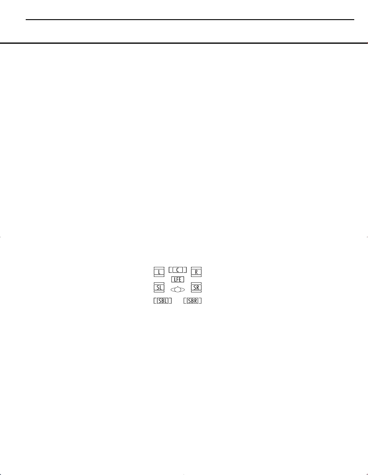
AVR140 harman/kardon
18
OPERATION
• When a DTS 5.1 signal is detected, you may listen
to it as a two-channel presentation, a 5.1-channel
presentation or a 6.1-channel presentation (if your
AVR is configured for 6.1 operation). To hear a twochannel presentation, scroll through the DTS surround modes until the Stereo icon lights in the
Surround Mode Indicators ˆ in addition to the
DTS icon. Continue scrolling to engage DTS 5.1
processing or DTS+Neo:6 (6-channel) processing.
• If a DTS-ES 6.1 Discrete signal is present, you may
choose a two-channel presentation, a 5.1-channel
presentation or a 6.1-channel presentation (if your
AVR has been configured for 6.1 operation). Scroll
through the DTS surround modes until the Stereo
icon lights in the
in addition to the DTS icon. Continue scrolling to
engage DTS 5.1 processing or DTS-ES Discrete
processing.
When a Dolby Digital signal with a 3/1/0 or 2/0/0
signal is detected you may select any of the Dolby
surround modes.
See page 33 for information on setting a default surround mode.
It is always a good idea to check the readout for the
channel data to make certain that it matches the audio
logo information shown on the back of a DVD package. In some cases you will see indication for “2/0/0”
even when the disc contains a full 5.1, or 3/2/.1 signal. When this happens, check the audio output settings for your DVD player or the audio menu selections
for the specific disc being played to make certain that
the player is sending the correct signal to the AVR.
PCM Audio Playback
PCM is the abbreviation for Pulse Code Modulation,
which is the type of digital signal used for standard CD
playback and other non-Dolby Digital and non-DTS
digital sources such as Mini-Disc.The digital circuits
in the AVR 140 are capable of high-quality digital-toanalog decoding, and they may be connected directly
to the digital audio output of your CD or LD player.
Connections may be made to either the rear-panel
Optical or Coaxial Inputs ·d or the front-panel
Digital Inputs *(.
To listen to a PCM digital source, first select the input for
the desired source (e.g., CD). Next press the
Select Button
Buttons n on the remote, or the‹/›Selector
Buttons
) on the front panel, until the desired choice
appears in the
During PCM playback, you may select any Surround
mode except Dolby Digital or DTS.
When a PCM signal is detected, the
Surround Mode Indicators ˆ
#q and then use the ⁄/
Upper Display Line P.
Lower Display
Digital
¤
ı will briefly show a message with the letters
Line
PCM, in addition to a readout of the sampling frequency of the digital signal. In most cases this will be
48kHz, though in the case of specially mastered,
high-resolution audio discs you will see a
indication.
Some DVD discs are recorded with both “5.1” and
“2.0” versions of the same sound-track. When playing
a DVD, always be certain to check the type of material
on the disc. Most discs show this information in the
form of a listing or icon on the back of the disc jacket.
When a disc does offer multiple soundtrack choices
you may have to make some adjustments to your
DVD player (usually with the “Audio Select” button or in
a menu screen on the disc) to send a full 5.1 feed to
the AVR 140. It is also possible for the type of signal
feed to change during the course of a DVD playback.
In some cases the menu screens and previews of
special material will only be recorded in 2.0 audio,
while the main feature is available in 5.1 audio.As
long as your DVD player is set for 6-channel output,
the AVR 140 will automatically sense changes to the
bitstream and channel count and reflect them in these
indicators.
Speaker/Channel Indicators
In addition to the bitstream indicators, the AVR 140
features a set of unique channel-input indicators that
tell you how many channels of digital information are
being received and/or whether the digital signal is
interrupted. (See Figure 9.)
Figure 9
These indicators are the L/C/R/LFE/SL/SR/SBL/SBR
letters that are inside the center boxes of the
Channel Input Indicators
Remember that the AVR 140 is capable of processing
a 7.1-channel signal, although you may only connect
one surround back speaker to it. It will automatically
combine the left and right surround back channel
information, and output it through the single surround
back speaker, if you have configured that speaker
using the
SPEAKER SIZE menu (Figure 8).
When a standard analog signal is in use, only the “L”
and “R” indicators will light, as
only left and right channels.
Digital signals, however, may have two, five, six or
seven channels, depending on the program material,
the method of transmission and the way in which it
was encoded. When a digital signal is playing, the let-
O on the front panel.
analog signals have
96kHz
Speaker/
ters in these indicators will light in response to the
specific signal being received. It is important to note
that although Dolby Digital, for example, is referred to
as a “5.1” system, not all Dolby Digital DVDs or programs are encoded for 5.1. Thus, it is sometimes normal for a DVD with a Dolby Digital soundtrack to trigger only the “L” and “R” indicators.
NOTE: Many DVD discs are recorded with both “5.1”
and “2.0” versions of the same soundtrack.When
playing a DVD, always be certain to check the type of
material on the disc. Most discs show this information
in the form of a listing or icon on the back of the disc
jacket. When a disc does offer multiple soundtrack
choices, you may have to make some adjustments to
your DVD player (usually with the “Audio Select” button
or in a menu screen on the disc) to send a full 5.1
feed to the AVR 140. It is also possible for the type
of signal feed to change during the course of a DVD
playback. In some cases, the menu screens and previews of special material will only be recorded in 2.0
audio, while the main feature is available in 5.1 audio.
The AVR 140 will automatically sense changes to the
bitstream and channel count and reflect them in these
indicators.
The letters used by the
Indicators
has been interrupted. This will happen when a digital
input source is selected before the playback starts, or
when a digital source such as a DVD is paused. The
flashing indicators remind you that the playback has
stopped due to the absence of a digital signal and not
through any fault of the AVR 140. This is normal, and
the digital playback will resume once the playback is
started again.
Night Mode
A special feature of Dolby Digital is the Night mode,
which enables specially encoded Dolby Digital input
sources to be played back with full digital intelligibility
while reducing the minimum peak level by 1/4 to 1/3.
This prevents abruptly loud transitions from disturbing
others, without reducing the impact of the digital
source.The Night mode is available only when Dolby
Digital signals with special data are being played.
The Night mode may be engaged when a Dolby
Digital DVD is playing by pressing the
Button
Buttons n to select either the middle range or
full compression versions of the Night mode.To turn
the Night mode off, press the
until the message in the lower third of the video display and in the
D-RANGE OFF.
O also flash to indicate when a bitstream
l on the remote. Next, press the ⁄/
Speaker/Channel Input
Night Mode
⁄/¤
Buttons n
Lower Display Line Q reads
¤
OPERATION 29OPERATION 29
Page 19

BridgeTM BridgeTM BridgeTM Bridge
T
M
Bridge
TM
AVR140 harman/kardon
19
OPERATION
OPERATION
The Night mode may also be selected to always be on
at either level of compression using the options in the
DOLBY menu. See page 19 for information on
using the menus to set this option.
IMPORTANT NOTES ON DIGITAL PLAYBACK:
• When the digital playback source is stopped, or in
a pause, fast-forward or chapter-search mode, the
digital audio data will momentarily stop, the channel
position letters inside the
Indicators
not indicate a problem with either the AVR 140 or
the source machine.The AVR 140 will return to digital playback as soon as the data is available and
when the machine is in a standard play mode.
• Although the AVR 140 will decode virtually all current
DVD movies, CDs and HDTV sources, it is possible
that some future digital sources may not be compatible with the AVR 140.
• Not all digitally encoded programs contain full 5.1or 6.1-channel audio. Consult the program guide
that accompanies the DVD or laser disc to determine which type of audio has been recorded on the
disc.The AVR 140 will automatically sense the type
of digital surround encoding used and adjust to
accommodate it.
• When some digital sources are playing, you may
not be able to select some of the analog surround
modes such as Dolby Pro Logic II or IIx, Dolby 3
Stereo, Hall, Theater or Logic 7.
• When a Dolby Digital or DTS source is playing, it is
not possible to make an analog recording using the
Tape Outputs £ and Video 1 Audio Outputs
k. However, the digital signals will be passed
through to the
O will flash. This is normal and does
Digital Audio Outputs fl‡.
Speaker/Channel Input
Tuner Operation
The AVR 140’s tuner is capable of tuning AM, FM and
FM Stereo broadcast stations. Stations may be tuned
manually, or they may be stored as favorite station
presets and recalled from a 30-position memory.
Station Selection
1. Press the AM/FM Tuner Select Button g on
the remote to select the tuner as an input. The
tuner may be selected from the front panel either
by pressing the
the tuner is active or by pressing the
Selector
2. Press the
Tuner Band Selector ! again to switch between
AM and FM so that the desired frequency band is
selected.
3. Press the
manual or automatic tuning.
Input Source Selector ^ until
Tuner Band
!.
AM/FM Tuner Select Button g or
Tuner Mode Button&I to select
When the button is pressed so that
appears in the Lower Display Line ı each
press of the
the tuner in a scan mode that seeks the next higher
or lower frequency station with acceptable signal
strength. An
will momentarily appear when the station stops
at a stereo FM station, and an
indication will momentarily appear when an AM or
monaural FM station is tuned. Press the Tuning buttons again to scan to the next receivable station.
When the button is pressed so that
appears in the Lower Display Line ı each tap
of the Selector will increased or decrease the frequency by one increment. When the tuner receives
a strong-enough signal for adequate reception,
MANUAL TUNED will appear in the Lower
Display Line
4. Stations may also be tuned directly in either the
automatic or manual mode.To enter a station’s frequency directly, first select the AM or FM band as
desired be pressing the
Button
Within five seconds of seeing the
scroll in the Upper Display Line P, enter the
station frequency by pressing the
r. If you press an incorrect button while entering
a direct frequency, press the
start over.
NOTE: When FM reception of a station is weak, audio
quality will be increased by switching to Mono mode
by pressing the
MANUAL appears momentarily in the Lower
Display Line
manual tuning mode.
Preset Tuning
Using the remote, up to 30 stations may be stored in
the AVR 140’s memory for easy recall using the front
panel controls or the remote.
To enter a station into the memory, first tune the
station using the steps outlined above.Then:
1. Press the
Two underscore lines will appear at the far right
side of the
2. Within five seconds, press the
corresponding to the location where you wish to
store this station’s frequency. Once entered, the
preset number will appear in the
Line
3. Repeat the process after tuning any additional
stations to be preset.
Tuning Selectors 9u will put
AUTO ST TUNED indication
ı.
AM/FM Tuner Select
g. Next, press the Direct Button J.
Tuner Mode Button&I so that
ı and goes out. This will also activate
Memory Button X on the remote.
Upper Display Line P.
P.
AUTO
AUTO TUNED
MANUAL
DIRECT IN
Numeric Keys
Clear Button W to
Numeric Keys r
Upper Display
Recalling Preset Stations
• To manually select a station previously entered in
the preset memory, press the
that correspond to the desired station’s memory
location.
• To manually tune through the list of stored preset
stations one by one, press the
Selector Buttons
remote.
$T on the front panel or
Numeric Keys r
Preset Stations
Recording
In normal operation, the audio or video source
selected for listening through the AVR 140 is sent to
the record outputs.This means that any program you
are watching or listening to may be recorded simply
by placing machines connected to the
£ or Video 1 Audio/Video and S-Video Outputs
ek in the Record mode.
When a digital audio recorder is connected to the
Digital Audio Outputs fl‡, you are able to record
the digital signal using a CD-R, MiniDisc or other digital
recording system.
NOTES:
• The digital outputs are active only when a digital sig-
nal is present, and they do not convert an analog
input to a digital signal, or change the format of the
digital signal. In addition, the digital recorder must
be compatible with the output signal. For example,
the PCM digital input from a CD player may be
recorded on a CD-R or MiniDisc, but Dolby Digital
or DTS signals may not.
• Please make certain that you are aware of any
copyright restrictions on any material you copy.
Unauthorized duplication of copyrighted materials
is prohibited by federal law.
Tape Outputs
Using
When Harman Kardon’s (optional) is connected
and a compatible Apple®iPod®is docked in The
Bridge, press the
d to choose the iPod as the input source. Pressing
the
activate the AVR remote’s control codes for the iPod,
and you may also use the front-panel controls to
operate the iPod. You may also select DMP
as the source from the front panel by repeatedly
pressing the
appears in the Upper Display Line P, although no
Input Indicator Ú will light.
When The Bridge is properly connected and a compatible iPod is properly docked, the
Line
that message appears, use the remote or front-panel
buttons to control the iPod. See the Function List
DMP Selector Button d will also
Input Source Selector ^ until DMP
P will read DMP/CONNECTED. Once
DMP Selector Button
Upper Display
30 OPERATION
Page 20

The
Bridge
TM
The
Bridge
T
M
AVR140 harman/kardon
20
OPERATION
Table on pages 37–38 for a listing of the remote
control buttons that have been programmed to
control the iPod. In brief, the
Play and Forward Search Buttons
⁄/¤/‹/›Buttons no and Set Button p
Reverse Search,
` and the
may be used in a similar manner to the corresponding
controls on the iPod. Additional buttons on the remote
may also be used to navigate your iPod’s albums
and playlists. Complete details on operating an iPod
using and an AVR remote are furnished
with .
The front-panel controls may be used to access a limited number of iPod functions. Press the
Button
& to play or pause the current track. The
Tuner Mode
Tuning Selector 9 may be used to search reverse
(left side of button) or forward (right side of button)
through the tracks. Press the
! to call up the iPod’s menu. Press the ‹/
Tuner Band Selector
›
Buttons ) to scroll, and the Set Button @ to
select.
Output Level Trim Adjustment
Normal output level adjustment for the AVR 140 is
established using the test tone, as outlined on pages
23–24. In some cases, however, it may be desirable
to adjust the output levels using program material such
as a test disc, or a selection you are familiar with.
Additionally, the output level for the subwoofer can
only be adjusted using this procedure.
To adjust the output levels using program material, first
set the reference volume for the front left and front right
channels using the Volume Control Òb
If you are using a disc with test signals or an external
signal generator as the source from which to trim the
output levels, you may use a handheld SPL meter to
guide you to the correct SPL levels. Set the meter to
the C-Weighting Slow scale, and adjust the volume
until the meter reads 75dB.
Once the reference level has been set, press the
Channel Select Buttonmand FRONT L
LEVEL
will appear in the Lower Display Line
Q and semi-OSD. To change the level, first press
the
Set Button p, and then use the ⁄/
Buttonsnto raise or lower the level. DO NOT
use the volume control, as this will alter the
reference setting.
Once the change has been made, press the
Button
p and then press the ⁄/¤Buttons
to select the next output channel location you wish to
adjust. To adjust the subwoofer level, press the
Buttonsnuntil WOOFER LEVEL appears in
the
Lower Display Line Q and on screen.
Repeat the procedure as needed until all channels
requiring adjustment have been set. When all adjust-
.
¤
Set
n
⁄/¤
ments have been made and no further adjustments
are made for five seconds, the AVR 140 will return to
normal operation.
The channel output for any input may also be adjusted
using the full-OSD on-screen menu system. First, set
the volume to a comfortable listening level using the
Volume Control Òb. Then, press the OSD
Button
v to bring up the MASTER MENU
(Figure 1). Press the ¤Button n until the on-
›
screen
cursor is next to the MANUAL
SETUP
the
⁄/¤ Buttons n to scroll to the CHANNEL
ADJUST
display the
line. Press the Set Button p to display
MANUAL SETUP submenu, and use the
line. Press the Set Button p again to
CHANNEL ADJUST submenu.
Once the menu appears on your video screen, first
⁄/¤
use the
›
cursor so that it is next to the TEST TONE
Buttons n to move the on-screen
line. Press the ‹/›Buttons o so that OFF
appears.This will turn off the test tone and allow you
to use your external test disc or other source material
as the reference.Then, use the
⁄/¤
Buttons n
until the › cursor is next to the TEST TONE
SEQ
line so that you may select between automatic
and manual movement of the test tone from one
channel to the next. When
AUTO appears, the test
tone will automatically circulate from one channel to
the next, pausing momentarily at each channel. If you
adjust the level of any channel, the test tone will
remain paused at that channel until several seconds
after your last adjustment before continuing to the next
channel. When
MANUAL appears, the test tone will
remain paused at the last channel until you use the
⁄/¤ Buttons n to select another channel.
At each channel position, use the
‹/›
Buttons o
to change the output level. Remember, the goal is to
have the output level at each channel be equal when
heard at the listening position. Regardless of the
method used to adjust the output levels, whether the
test tone or an external source is used, remember that
when the AVR is configured for 6.1 operation with only
a single surround back speaker, you will still have an
output adjustment for both a surround back left and
surround back right speaker location even though
there is only one speaker. This is not a duplicate
adjustment. Rather, it is needed so that the proper balance is achieved for 7.1-channel processing modes
when the discrete surround back channels are mixed
to a single output.
If you wish to reset all the levels to their original
factory default of 0dB offset, press the
⁄/¤
Buttons
n so that the on-screen cursor is next to the
CHANNEL RESET line and press the ‹/
Buttons o so that the word ON appears.
›
After the
levels are reset, resume the procedure outlined above
to reset the levels to the desired settings.When all
adjustments are done, press the
⁄/¤
Buttons
n
to move the on-screen ›cursor so that it is next to
BACK TO MANUAL SETUP and then press
the
Set Button p if you wish to go back to the
manual setup menu to make other adjustments. If you
have no other adjustments to make, press the
Button
v to exit the menu system.
OSD
NOTE: The output levels may be separately trimmed for
each digital and analog surround mode. If you wish to
have different trim levels for a specific mode, select that
mode and then follow the instructions in the steps shown
earlier.
Memory Backup
This product is equipped with a memory backup system that preserves the system configuration information
and tuner presets if the unit is accidentally unplugged
or subjected to a power outage.This memory will last
for approximately four weeks, after which time all information must be reentered.
OPERATION 31OPERATION 31
Page 21

AVR140 harman/kardon
21
TROUBLESHOOTING GUIDE
SYMPTOM CAUSE SOLUTION
Unit does not function when Main • No AC Power • Make certain AC power cord is plugged into
Power Switch is pushed a live outlet
• Check to see whether outlet is switch-controlled
Display lights, but no sound • Intermittent input connections • Make certain that all input and speaker connections
or picture are secure
•
Mute is on • Press Mute Button f
• Volume control is down • Turn up volume control
No sound from any speaker; • Amplifier is in protection mode • Check speaker wire connections for shorts at receiver and
light around power switch is red due to possible short speaker ends
• Amplifier is in protection mode • Contact your local Harman Kardon service center
due to internal problems
No sound from surround or • Incorrect surround mode • Select a mode other than Stereo
center speakers • Input is monaural • There is no surround information from mono sources
• Incorrect configuration • Check speaker mode configuration
• Stereo or Mono program material • The surround decoder may not create center- or rear-channel
information from nonencoded programs
Unit does not respond to • Weak batteries in remote • Change remote batteries
remote commands • Wrong device selected • Press the AVR selector
• Remote sensor is obscured • Make certain front panel sensor is visible to remote
or connect remote sensor
Intermittent buzzing in tuner • Local interference • Move unit or antenna away from computers, fluorescent
lights, motors or other electrical appliances
Letters flash in the channel indicator • Digital audio feed paused • Resume play for DVD
display and digital audio stops • Check that Digital Input is selected
In addition to the items shown above, additional information on troubleshooting possible problems with your AVR 140, or installation-related issues, may be found in the list of
"Frequently Asked Questions" which is located in the Product Support section of our Web site at www.harmankardon.com.
Processor Reset
In the rare case where the unit’s operation or the displays seem abnormal, the cause may involve the erratic
operation of the system’s memory or microprocessor.
To correct this problem, first unplug the unit from the
AC wall outlet and wait at least three minutes. After the
pause, reconnect the AC power cord and check the
unit’s operation. If the system still malfunctions, a system reset may clear the problem.
NOTE: Resetting the processor will erase any configuration settings you have made for speakers, output
levels, surround modes, digital input assignments as
well as the tuner presets.The unit will be returned to
the factory presets, and all settings for these items
must be reentered.
If the system is still operating incorrectly, there may
have been an electronic discharge or severe AC line
interference that has corrupted the memory or
microprocessor.
To clear the AVR 140’s entire system memory including tuner presets, output level settings, delay times and
speaker configuration data, first place the AVR in
Standby Mode, and then press and hold the
Mode Button
will turn on automatically.
5 button for three seconds. The unit
Tone
If these steps do not solve the problem, consult an
authorized Harman Kardon service center.
TROUBLESHOOTING GUIDE 49
Page 22
CHR@RRDLAKX
22
AVR140 harman/kardon
@UQ03/
0-QdlnuhmfsgdSnoB`ahmds
QdlnudsgdRbqdvr
5
3
4
8
7
6
5
4
02
0
}
0/
8
00
0
1
1-QdlnuhmfsgdEqnmsO`mdk
QdlnudsgdRbqdvr
3
0
1
2
2-QdlnuhmfsgdQd`qO`mdk
QdlnudsgdRbqdvr
7
6
7
01
02
2
8
0/
00
01
02
03
6
13
15
0
}
354 2 1 0 06 07
14 16 17
15 18 2/
08
0504
20
111/ 10
12
3-QdlnuhmfsgdL`hmOBA
0 7
}
5
3
7
6
0 8
QdlnudsgdRbqdvr
}
0
4
1
2
Page 23
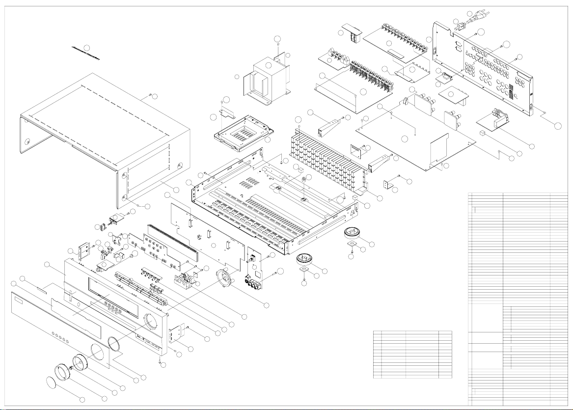
23
24
@UQ03/DWOKNCDUHDV
36
R0
26,8
EXPLODED
25
3/,4
R3
18
R8
3/,3
2/
R01
27,1
3/,0
3/,2
R00
R4
33
32
28,0
R5
21
w1
R3
27,0
R3
R4
R4
11
10
1/
R6
R1
26,4
04
26,5
R1
R1
03
R1
8
7
6
5
02
26,3
R2
05
26,0
R1
26,7
26,2
35
17
R0/
R1
R03
13
12
R3
12
R3
R4
R4
16
15
14
13
08
06
01
00
0/
R1
8
R0
R0
4
3
2
1
0
07
CDRBQHOSHNM O@QSRMN- P+sx
MN
R0
RBQDV
RBQDV
RBQDV
RBQDV
RBQDV
RBQDV
RBQDV
RBQDV+SQ@MR
RBQDV
RBQDV+RODBH@K
RBQDV+RODBH@K
RBQDV
RBQDV
BSA2*0/F
BSVR2*0/F
BSV2*7I
BSA2*7I
BSV2*01I
BSA3*5EEB
BSA2*0/FEY
BGC0@/12
BSA2*5I
BGC0@/01Y
BGC3@/01
BSA2*7IEY
BSA2*05FEY
R1
R2
R3
R4
R5
R6
R7
R8
R0/
R00
R01
R02
R03
23
22
R02
R02
R7
20
30
3/,1
R0/
31
34
R3
CDRBQHOSHNM
MN
B@O+UNKTLD
0
GNKCDQ+UNKTLD
1
HMCHB@SNQ+UNKTLD
2
VHMCNV@RR&X
3
VHMCNV+EHO BFT0@255W
0
A@CFD+LNCDK
1
4
EHKSDQ+EHO
5
AC@FD+G@QL@M.J@QCNM
6
O@MDK+EQNMS
7
AQ@BJDS+RHCD
8
JMNA+ETMBSHNM
0/
JMNA+RDS
00
JMNA+CDK@X
01
JMNA+ONVDQ
02
HMCHB@SNQ+ONVDQ
03
JMNA+LNLR
04
AQ@BJDS+OBA BLJ0@/0/
05
OK@SD+RGHDKC
06
NQM@LDMS+UNKTLD BFT0@207Y 0
07
GNKCDQ+KDC
08
AQ@BJDS+EHO
1/
B@AHMDS+SNO
10
BG@RRHR+ANSSNL
11
QTAADQ+BTRGHNM
12
ENNS
13
RTOONQS+BTRGHNM
14
GD@SRHMJ
15
AQ@BJDS+OBA
16
GNKCDQ+OBA
17
AQ@BJDS+SQ@MR
18
AQ@BJDS+OBA'G.S(
2/
AQ@BJDS+OBA BLC0@46/ 0
20
AQ@BJDS+OBA
21
O@MDK+QD@Q
22
ATRGHMF+@BBNQC
23
BNQC+ONVDQ
24
SQ@MR+ONVDQ
25
EQNMSO@A@RR&X
26
L@HMOBA@RR&X BNO00724A 0
27
06BSA2*7IEBRBQDV
24
0
HMOTSOBA@RR&X BNO00703D 0
28
8
0/
2
UHCDNOBA@RR&X3/BNO00705A 0
5
18
3
08
1
HONCOBA@RR&X BNO00723A 0
30
4
STMDQLNCTKD
31
2
OK@SD+RGHDKC 0BLB0@173
32
1
BTRGHNM 0BGF0@107
33
BTRGHNM+QTAADQ
34
BTRGHNM
35
A@CFD@RR&X
36
NQM@LDMS+A@CFD
0
A@CFD+G.J'SNO(
1
R3
O@QSRMNBFW0@227LAF16
BLG0@103
BFK0@111
BFT@UQ03/
JFA0@044Y
BLY1@/8/RGDDS+UNKTLD 0
BLY0@/77
JFA0@047Y
BFV0@3/7QCYG32
BLC1@332
BAS0@8/4LAYF16
BAS0@8/3LAYF16
BAS0@708J017
BAS0@8/2LLXF16
BFK0@110
BAB0@036LAYF16
BLB0@1//
BLG0@104
BLC0@1/8
BJB4A034R35
BT@0@118
JGF0@/4/
BJK1@/58G32
BGF0@0/3
BLX0@137
BLC0@306
BGD0@06/
BLC0@376
BLC0@287
BLC0@276
BJE03@143Y
JGQ0@/17
BI@412EAX@
BKS4U/23YT
BNO00707A
EHOOBA
26,0
JDXOBA
26,1
SNMDOBA
26,2
OGNMDOBA
26,3
LNLROBA
26,4
ONVDQKDCOBA
26,5
BNMMDBSNQOBA
26,6
CHFHS@KHMOTSOBA
26,7
CNVMKN@COBA 0
26,8
L@HMOBA
27,0
@BNTSKDSROBA
27,1
QDLNSDOBA
27,2
HMOTSOBA
28,0
LTKSHNTSOBA 0
28,1
UHCDNOBA 0
3/,0
BNLONMD@MSUHCDNOBA
3/,1
CHFHS@KHMOTS.NTSOTSOBA
3/,2
SQ@MROBA
3/,3
SQ@MROBA
3/,4
BMUL8/00LR/60K
BGF0@046
BGF0@05/
BFW0@264Y@
BFW0@264L6F21
JFA0@048Y
P+sx
0
0
0
0
0
0
0
0
0
1
0
0
0
0
0
0
0
0
0
2
0
0
3
3
0
0
1
1
0
1
1
0
0
0
0
0
0
0
0
0
0
0
0
0
0
0
0
0
0
0
0
0
0
0
0
0
0
0
0
0
Page 24

AVR140 harman/kardon
24
Page 25
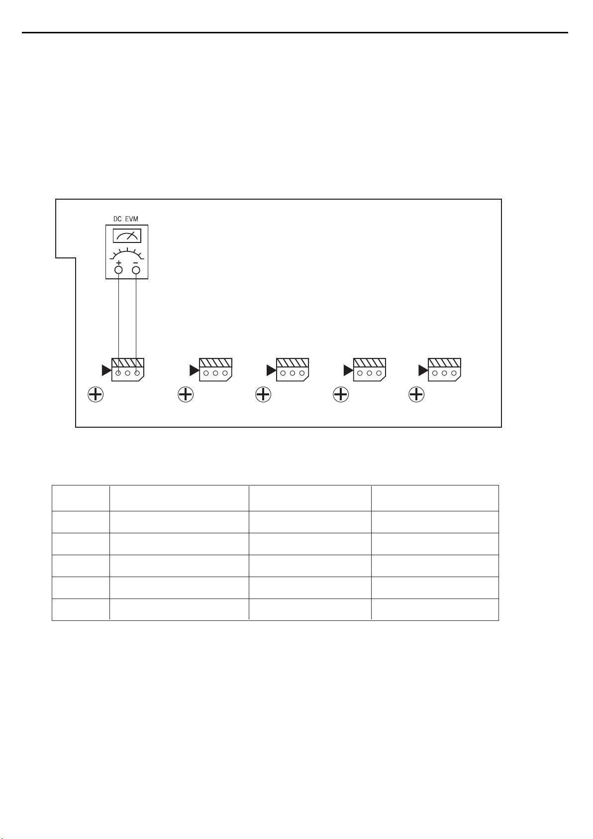
AVR140 harman/kardon
25
AMPLIFIER SECTION BIAS ADJUSTMENT
Measurement condition
. No input signal or volume position is minimum.
Standard value.
. Ideal current = 48mA ( ± 5%)
. Ideal DC Voltage = 25.92mV ( ± 5%)
CUP11816Z (VIDEO PCB)
...... ......
VR87
CN81
VR86
CN82
VR82
CN86
VR81
DC VOLTMETER..............Connect to CN81,CN82,CN83,CN84,CN85,CN86,CN87
NO. Channel Adjust for
1 Front Left 25.92mV (±5%)
2 Front Right 25.92mV (±5%)
3 Center
4 Surround Left
5 Surround Right
6
7
Surround Back Left
Surround Back Right
25.92mV (±5%)
25.92mV (±5%)
25.92mV (±5%)
25.92mV (±5%)
25.92mV (±5%)
Adjustment
VR81(ONLY AVR240/340)
CN87
VR83
VR84
VR85
VR86
VR87
VR82
Page 26
AVR140 harman/kardon
26
harman/kardon Service Bulletin
Service bulletin # HK2006-01 January 2006
To: All harman/kardon Service Centers
Models: AVR135, AVR140, AVR240, AVR340,
AVR135/230v, AVR235/230v, AVR335/230v, AVR140/230v, AVR240/230v, AVR340/230v
Subject: Defective Wafer
In the event you receive an AVR135, AVR140, AVR240, AVR340, AVR135/230v, AVR235/230v,
AVR335/230v, AVR140/230v, AVR240/230v, or AVR340/230v receiver with the complaint “there is no
On Screen Display (OSD) output through the Composite, S-video, or Component Video* connec tions,
or no video pass-through from S-Video or Composite connections”, perform the following procedure:
Synopsis: Flat flex cable assembly possibly not making a good contact with defective wafer connector CN72,
located on the Input PCB.
Check to see if the affected unit falls into the serial number range(s) below, which may need modification.
1) Remove the top cover
2) Remove the Tuner PCB and Video PCB’s.
3) Remove the Input PCB; replace 16 pin wafer connector CN72 with h/k part# KJP32GA117ZG.
4) Replace all PCB’s in reverse order, and the top cover.
5) Test the unit.
MODEL
AVR135
AVR140
AVR240
AVR340
AVR135 in
CP15 system
AVR235 in
CP25 system
AVR335 in
CP35 system
AVR135/230
AVR235/230
AVR335/230
AVR140/230
AVR240/230
AVR340/230
* Note: For the models above, excluding the AVR340, the full On Screen Display (OSD) normally will not be visible with Component
video connections alone. For model AVR340, when the component video jacks are used, the onscreen menus are not visible with
high-definition video (720p or 1080i), and you must switch to the standard composite or S-video input on your TV, or to a 480p video
source, to view them.
harman/kardon, Incorporated 250 Crossways Park Dr. Woodbury, New York 11797
SERIAL NUMBER (120V) SERIAL NUMBER (230V) STATUS ACTION
AN0020-28676 to
AN0020-33475
AN0031-04201 to
AN0031-16800
AN0032-01001 to
AN0032-13000
AN0033-01001 to
AN0033-09000
AN0023-08026 to
AN0023-09825
AN0024-03001 to
AN0024-04000
AN0025-04101 to
AN0025-05100
Warranty labor rate: MINOR repair
AN0027-14356 to
AN0027-17965
AN0028-11601 to
AN0028-20300
AN0029-07401 to
AN0029-09830
AN0034-01001 to
AN0034-04600
AN0035-01001 to
AN0035-03400
AN0036-01001 to
AN0036-02200
May Need
Modification
May Need
Modification
May Need
Modification
May Need
Modification
May Need
Modification
May Need
Modification
May Need
Modification
May Need
Modification
May Need
Modification
May Need
Modification
May Need
Modification
May Need
Modification
May Need
Modification
Replace Wafer
Replace Wafer
Replace Wafer
Replace Wafer
Replace Wafer
Replace Wafer
Replace Wafer
Replace Wafer
Replace Wafer
Replace Wafer
Replace Wafer
Replace Wafer
Replace Wafer
Page 27

AVR140 harman/kardon
27
harman/kardon TECH TIPS
Troubleshooting tips and solutions to common service problems
For models:
AVR7000/7200/7300/8000
AVR100/200/300/500
AVR110/210/310/510
AVR120/220/320/520
AVR125/225/325/525
AVR130/230/330/430/630
AVR135/235/335/435/635
AVR140/240
Subject: Backup Memory on AVR/DPR/HK series receivers
In the event of the complaint: “the receiver is losing its memory (any programmed system settings)
when the unit is turned off, or after the unit is unplugged (briefly*)”:
Check and replace:
Model Designator Location Description Part number
AVR10
AVR7000 C730 Front PCB 0.047 Farad 5.5v capacitor
AVR7200 C106 Front PCB 0.047 Farad 5.5v capacitor # P10790-ND
AVR7300 C657 DSP PCB 0.047 Farad 5.5v capacitor # H01-CEZXA0479MN-5
AVR8000 C726 Front PCB 0.047 Farad 5.5v capacitor
AVR100/200 C412 Front PCB 0.047 Farad 5.5v capacitor # CEGT-B473J-0J0
AVR300 C906 Front PCB 0.1Farad 5.5v capacitor
AVR500 C906 Front PCB 0.1Farad 5.5v capacitor
AVR110/210/310/510
AVR120/220/320/520
AVR125/225 C734,C885 Front PCB two 0.1F capacitors in parallel # BCESOHD104
AVR325/525 C106 Front PCB 0.047 Farad 5.5v capacitor # P10790-ND
AVR130/230/330 BAT1 Front PCB 3.6v Battery # HABGP40BVH3A3H
AVR135/235/335 BAT1 Front PCB 3.6v Battery # HGP15BNH3A3H
AVR140/240 BAT1 Front PCB 3.6v Battery # HABGP40BVH3A3H
AVR430/630 C657 DSP PCB 0.047 Farad 5.5v capacitor # CEZXA0479MN-5
AVR435/635 C557 DSP PCB 0.047 Farad 5.5v capacitor # H03-CEZXA0479MN-0
DPR1001 BC601 Main PCB 0.1Farad 5.5v capacitor # CEGT-B104J-0J0
DPR1005/2005 C437
HK3370/3470 C301 Front PCB 0.1Farad 5.5v capacitor # CEGT-B104J-0J0
HK3375/3475 C301 Front PCB 0.1Farad 5.5v capacitor # CEGT-B104J-0J0
HK3250
* After approximately two weeks of being disconnected from AC supply, even a normally functioning receiver may lose
any programmed settings and switch to default settings. (Four weeks for the DPR1005 & 2005)
C712
D709
C216 Front PCB 0.047 Farad 5.5v capacitor # P10790-ND
C712
D709
AVR10
DPR1001
DPR1005
DPR2005
HK3370/3470/3375/3475
HK3250
Front PCB
Processor
PCB
Front PCB
0.047 Farad 5.5v capacitor
and 1N4148 diode
0.047 Farad 5.5v capacitor # CEZXA0479MN-5
0.047 Farad 5.5v capacitor
and 1N4148 diode
TIP# HKTT2003-01 Rev6
#3439247315
#2058322101
# P10790-ND or
# J3432147324X
# 55230310NR or
# P10790-ND
# J4433210421X
or # P10791-ND
# J4433210421X
or # P10791-ND
#3439247315
#2058322101
Page 28
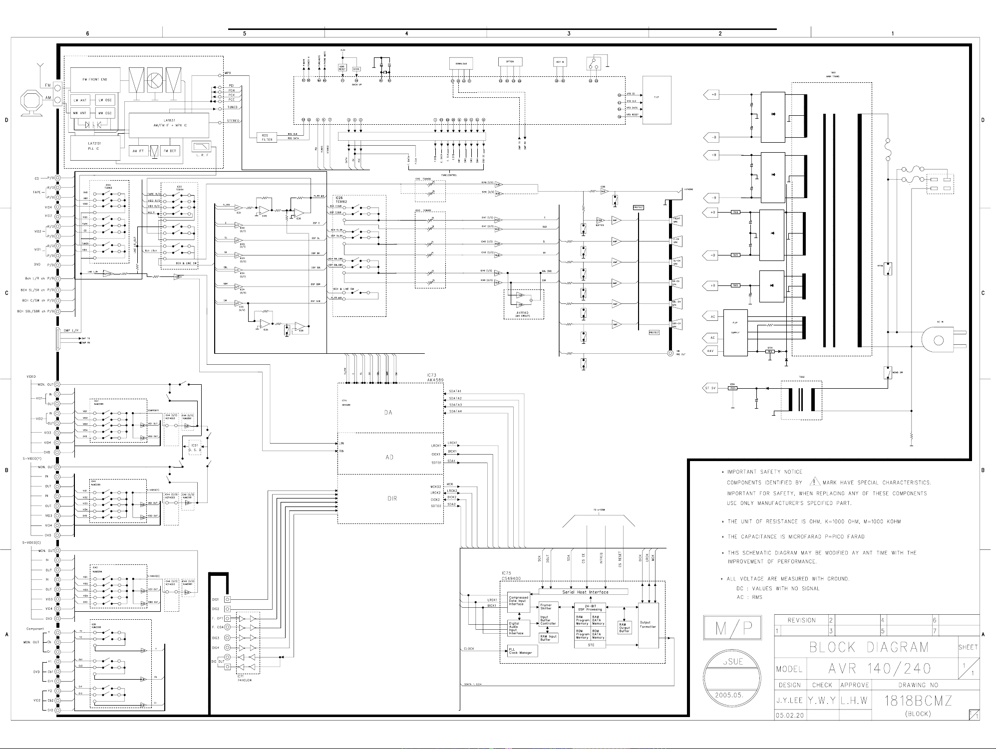
AVR140 harman/kardon
28
Page 29
CAM350PROV7.6:MonSep0110:29:562003-(Untitled)
29
MAIN BOARD 1 (AMP)
AVR140 harman/kardon
Page 30
AVR140 harman/kardon
30
Page 31

AVR140 harman/kardon
31
Page 32

AVR140 harman/kardon
32
Page 33

AVR140 harman/kardon
33
Page 34

AVR140 harman/kardon
34
Page 35

AVR140 harman/kardon
35
AVR140 Electrical Parts List
Ref. Designator Part Number
Description
Qty
FRONT PCB ASSY (CUP11818Y)
Capacitors
C703 HCBS1H821KBT CAP , CERAMIC 820PF 50V K 1 EA
C704 CCEA1VH100T CAP , ELECT 10UF 35V 1 EA
C712 CCEA1HH1R0T CAP , ELECT 1UF 50V 1 EA
C713 HCBS1H223ZFT CAP , CERAMIC 0.022UF 50V Z 1 EA
C714 HCBS1H151KBT CAP , CERAMIC 150PF 50V K 1 EA
C716 CCEA1CH331T CAP , ELECT 330UF 16V 1 EA
C723 HCBS1H104ZFT CAP , CERAMIC 0.1UF 50V Z 1 EA
C725 HCBS1H473ZFT CAP , CERAMIC 0.047UF 50V Z 1 EA
C726 CCEA1CH101T CAP , ELECT 100UF 16V 1 EA
C728 HCBS1H104ZFT CAP , CERAMIC 0.1UF 50V Z 1 EA
C729 CCKT1H473ZF CAP , CERAMIC 0.047UF 50V ZF 1 EA
C731 CCEA1HH100T CAP , ELECT 10UF 50V 1 EA
C735 CCEA1CH101T CAP , ELECT 100UF 16V 1 EA
C736 HCBS1H223ZFT CAP , CERAMIC 0.022UF 50V Z 1 EA
C737 HCBS1H180JCT CAP , CERAMIC 18PF 50V J 1 EA
C738 HCBS1H180JCT CAP , CERAMIC 18PF 50V J 1 EA
C739 CCEA1AH221T CAP , ELECT 220UF/10V 1 EA
C740 CCEA1VH100T CAP , ELECT 10UF 35V 1 EA
C793 HCBS1H104ZFT CAP , CERAMIC 0.1UF 50V Z 1 EA
C794 HCBS1H102KBT CAP , CERAMIC 1000PF 50V B 1 EA
C795 HCBS1H221KBT CAP , CERAMIC 220PF 50V K 1 EA
C796 HCBS1H101KBT CAP , CERAMIC 100PF 50V K 1 EA
C859 HCBS1H223ZFT CAP , CERAMIC 0.022UF 50V Z 1 EA
C860 HCBS1H223ZFT CAP , CERAMIC 0.022UF 50V Z 1 EA
C861 HCBS1H223ZFT CAP , CERAMIC 0.022UF 50V Z 1 EA
C875 HCBS1H101KBT CAP , CERAMIC 100PF 50V K 1 EA
C876 HCBS1H101KBT CAP , CERAMIC 100PF 50V K 1 EA
C877 HCBS1H473ZFT CAP , CERAMIC 0.047UF 50V Z 1 EA
C878 HCBS1H473ZFT CAP , CERAMIC 0.047UF 50V Z 1 EA
C882 HCBS1H104ZFT CAP , CERAMIC 0.1UF 50V Z 1 EA
C886 CCEA0JH102T CAP , ELECT 1000UF 6.3V 1 EA
C891 HCBS1H223ZFT CAP , CERAMIC 0.022UF 50V Z 1 EA
C892 HCBS1H223ZFT CAP , CERAMIC 0.022UF 50V Z 1 EA
C893 HCBS1H223ZFT CAP , CERAMIC 0.022UF 50V Z 1 EA
C896 HCBS1H223ZFT CAP , CERAMIC 0.022UF 50V Z 1 EA
C897 CCEA1AH471T CAP , ELECT 470UF 10V 1 EA
C901 HCBS1H390JT CAP , CERAMIC 39PF 50V J 1 EA
C903 CCEA1HKS2R2T CAP , ELECT 2.2UF 50V KS 1 EA
C905 CCEA1HKS2R2T CAP , ELECT 2.2UF 50V KS 1 EA
C894 CCEA1CH101T CAP , ELECT 100UF 16V 1 EA
Semiconductors
D724 HVD1SS133MT DIODE 1SS133 1 EA
D728 HVD1SS133MT DIODE 1SS133 1 EA
D729 HVD1SS133MT DIODE 1SS133 1 EA
D730 HVD1SS133MT DIODE 1SS133 1 EA
D778 KVD1N4003ST DIODE 1N4003 1 EA
D779 HVD1SS133MT DIODE 1SS133 1 EA
D780 HVD1SS133MT DIODE 1SS133 1 EA
D781 HVD1SS133MT DIODE 1SS133 1 EA
D782 KVD1N4003ST DIODE 1N4003 1 EA
D783 HVD1SS133MT DIODE 1SS133 1 EA
IC87 HVIRE5VL28CATZ IC , RESET (RE5VL28CATZ) RICOH 1 EA
Q701 HVTKRC107MT TRANSISTOR KRC107M 1 EA
Q705 HVTKRC107MT TRANSISTOR KRC107M 1 EA
Q722 HVTKRA107MT TRANSISTOR KRA107M 1 EA
Page 36

AVR140 harman/kardon
36
Ref. Designator Part Number
Description
Qty
FRONT PCB ASSY (CUP11818Y)
Q724 HVTKRC107MT TRANSISTOR KRC107M 1 EA
Q725 HVTKRC107MT TRANSISTOR KRC107M 1 EA
Q726 HVTKRC107MT TRANSISTOR KRC107M 1 EA
Q727 HVTKRC107MT TRANSISTOR KRC107M 1 EA
Q728 HVTKRC107MT TRANSISTOR KRC107M 1 EA
Q729 HVTKRC107MT TRANSISTOR KRC107M 1 EA
Q738 HVTKRC107MT TRANSISTOR KRC107M 1 EA
Q739 HVTKTA1271YT TRANSISTOR KTA1271Y 1 EA
Q740 HVTKRC107MT TRANSISTOR KRC107M 1 EA
Q743 HVTKRA107MT TRANSISTOR KRA107M 1 EA
IC72 BVIMB90F482APFG140 IC , FLASH U-COM (MB90F482APFG) FUJITSU 1 EA
IC73 HRVNJL34H380A SENSOR , REMOTE (NJL34H380A) SENSOR 1 EA
IC75 HVI74ACT04MTR I.C , HEX (74ACT04) FAIRCHILD 1 EA
IC83 HVI74ACT04MTR I.C , HEX (74ACT04) FAIRCHILD 1 EA
IC84 HVI74ACT04MTR I.C , HEX (74ACT04) FAIRCHILD 1 EA
IC85 HVIRH5VT18C I.C , RESET (RH5VT18C) RICOH 1 EA
Resistors
R700 CRD20TJ102T RES , CARBON 1K OHM 1/5W J 1 EA
R701 CRD20TJ103T RES , CARBON 10K OHM 1/5W J 1 EA
R704 CRD20TJ100T RES , CARBON 10 OHM 1/5W J 1 EA
R709 CRD20TJ470T RES , CARBON 47 OHM 1/5W J 1 EA
R710 CRD20TJ470T RES , CARBON 47 OHM 1/5W J 1 EA
R711 CRD20TJ470T RES , CARBON 47 OHM 1/5W J 1 EA
R712 CRD20TJ102T RES , CARBON 1K OHM 1/5W J 1 EA
R713 CRD20TJ102T RES , CARBON 1K OHM 1/5W J 1 EA
R714 CRD20TJ102T RES , CARBON 1K OHM 1/5W J 1 EA
R716 CRD20TJ102T RES , CARBON 1K OHM 1/5W J 1 EA
R718 CRD20TJ222T RES , CARBON 2.2K OHM 1/5W J 1 EA
R722 CRD20TJ1R0T RES , CARBON 1 OHM 1/5W J 1 EA
R730 CRD20TJ112T RES , CARBON 1.1K OHM 1/5W J 1 EA
R731 CRD20TJ223T RES , CARBON 22K OHM 1/5W J 1 EA
R732 CRD20TJ222T RES , CARBON 2.2K OHM 1/5W J 1 EA
R733 CRD20TJ272T RES , CARBON 2.7K OHM 1/5W J 1 EA
R734 CRD20TJ103T RES , CARBON 10K OHM 1/5W J 1 EA
R735 CRD20TJ103T RES , CARBON 10K OHM 1/5W J 1 EA
R736 CRD20TJ272T RES , CARBON 2.7K OHM 1/5W J 1 EA
R737 CRD20TJ100T RES , CARBON 10 OHM 1/5W J 1 EA
R747 CRD20TJ103T RES , CARBON 10K OHM 1/5W J 1 EA
R750 CRD20TJ223T RES , CARBON 22K OHM 1/5W J 1 EA
R771 CRD20TJ103T RES , CARBON 10K OHM 1/5W J 1 EA
R772 CRD20TJ103T RES , CARBON 10K OHM 1/5W J 1 EA
R773 CRD20TJ103T RES , CARBON 10K OHM 1/5W J 1 EA
R780 CRD20TJ100T RES , CARBON 10 OHM 1/5W J 1 EA
R781 CRD20TJ123T RES , CARBON 12K OHM 1/5W J 1 EA
R786 CRD20TJ152T RES , CARBON 1.5K OHM 1/5W J 1 EA
R787 CRD20TJ101T RES , CARBON 100 OHM 1/5W J 1 EA
R789 CRD20TJ102T RES , CARBON 1K OHM 1/5W J 1 EA
R790 CRD20TJ105T RES , CARBON 1M OHM 1/5W J 1 EA
R791 CRD20TJ822T RES , CARBON 8.2K OHM 1/5W J 1 EA
R792 CRD20TJ102T RES , CARBON 1K OHM 1/5W J 1 EA
R820 CRD20TJ103T RES , CARBON 10K OHM 1/5W J 1 EA
R824 CRD20TJ221T RES , CARBON 220 OHM 1/5W J 1 EA
R825 CRD20TJ681T RES , CARBON 680 OHM 1/5W J 1 EA
R881 CRD20TJ103T RES , CARBON 10K OHM 1/5W J 1 EA
R882 CRD20TJ103T RES , CARBON 10K OHM 1/5W J 1 EA
R883 CRD20TJ103T RES , CARBON 10K OHM 1/5W J 1 EA
R884 CRD20TJ103T RES , CARBON 10K OHM 1/5W J 1 EA
R885 CRD20TJ103T RES , CARBON 10K OHM 1/5W J 1 EA
R886 CRD20TJ103T RES , CARBON 10K OHM 1/5W J 1 EA
Page 37

AVR140 harman/kardon
37
Ref. Designator Part Number
Description
Qty
FRONT PCB ASSY (CUP11818Y)
R887 CRD20TJ103T RES , CARBON 10K OHM 1/5W J 1 EA
R888 CRD20TJ103T RES , CARBON 10K OHM 1/5W J 1 EA
R889 CRD20TJ103T RES , CARBON 10K OHM 1/5W J 1 EA
R890 CRD20TJ103T RES , CARBON 10K OHM 1/5W J 1 EA
R891 CRD20TJ103T RES , CARBON 10K OHM 1/5W J 1 EA
R892 CRD20TJ222T RES , CARBON 2.2K OHM 1/5W J 1 EA
R893 CRD20TJ333T RES , CARBON 33K OHM 1/5W J 1 EA
R913 CRD20TJ102T RES , CARBON 1K OHM 1/5W J 1 EA
R915 CRD20TJ473T RES , CARBON 47K OHM 1/5W J 1 EA
Miscellaneous
FIP1 HFLHCA18ML03 F.I.P FIP 1 EA
L702 HLQ02C100KT COIL , AXAIL 10UH 1 EA
BAT1 HABGP40BVH3A3H BATTERY , RECHARGEABLE BATTERY 1 EA
BK71 CMD1A209 BRACKET , FLT BRACKET 1 EA
BK72 CMD1A209 BRACKET , FLT BRACKET 1 EA
BK73 CMD1A387 BRACKET , PCB BRACKET 1 EA
BK74 CMD1A209 BRACKET , FLT BRACKET 1 EA
BN15 CWB2B908150EN WIRE ASS'Y WIRE 1 EA
BN62 CWB2B904370EN WIRE ASS'Y WIRE 1 EA
BN72 HJP32GA179ZJ CONN,FFC 1M/M 32P STR,SMD_JST CONNECTOR 1 EA
BN80 CWB2B911420EW WIRE ASS'Y WIRE 1 EA
BN81 CWB2B908250BM WIRE , ASS'Y WIRE 1 EA
BN84 CWB2B905080EN WIRE ASS'Y WIRE 1 EA
BN85 CWB2B902090EN WIRE ASS'Y WIRE 1 EA
BN88 CWB2B904070EN WIRE ASS'Y WIRE 1 EA
CN89 CJP05GA19ZY WAFER, STRAIGHT, 5PIN WIRE 1 EA
JW85 CWE8202070AA WIRE ASS'Y WIRE 1 EA
X701 HOX05000E160C CRYSTAL 5Mhz 1 EA
PCB , MOMS (CUP11818-5)
SW1 CSH1A008ZV SW , PUSH (MOMS) MOMS SWITCH 1 EA
CN86 KJP02GA89ZM WAFER WIRE 1 EA
PCB , POWER KEY (CUP11818-6)
CN88 CJP04GA19ZY WAFER, STRAIGHT, 4PIN WIRE 1 EA
D723 CVD50BOBBWGA L.E.D , 2 COLOR (ORG , BLUE) L.E.D 1 EA
S701 HST1A020ZT SW , TACT 1A020 1 EA
PCB , DIGITAL INPUT (FRONT) (CUP11818-8)
BN18 CWZAVR125BN18 WIRE ASS'Y (SHIELD) WIRE 1 EA
IC76 HVI74HCU04AFNG I.C , INVERTER (74HCU04) TOSHIBA 1 EA
JK81 CJJ4M041Y JACK , BOARD (COAX) BOARD 1 EA
JK82 HJSTORX177L MODULE , OPTICAL(RX) OPTICAL JACK 1 EA
JW83 CWE8202150RV WIRE ASS'Y WIRE 1 EA
C807 CCFT1H104ZF CAP , SEMICONDUCTOR 0.1UF 50V ZF 1 EA
C808 CCKT1H181KB CAP , CERAMIC 180PF 50V KB 1 EA
C809 CCEA1AH471T CAP , ELECT 470UF 10V 1 EA
C812 HCBS1H104ZFT CAP , CERAMIC 0.1UF 50V Z 1 EA
C817 HCBS1H100JCT CAP , CERAMIC 10PF 50V J 1 EA
R805 CRD20TJ104T RES , CARBON 100K OHM 1/5W J 1 EA
R806 CRD20TJ472T RES , CARBON 4.7K OHM 1/5W J 1 EA
R869 CRD20TJ750T RES , CARBON 75 OHM 1/5W J 1 EA
R875 CRD20TJ103T RES , CARBON 10K OHM 1/5W J 1 EA
Page 38

AVR140 harman/kardon
38
Ref. Designator Part Number
Description
Qty
PCB , DOWNLOAD (CUP11818-9)
BN44 CWB2B904350EN WIRE ASS'Y WIRE 1 EA
CN82 KJP06HA37ZM WAFER WIRE 1 EA
CN15 CJP08GA19ZY WAFER, STRAIGHT, 8PIN WIRE 1 EA
R861 CRD20TJ101T RES , CARBON 100 OHM 1/5W J 1 EA
R862 CRD20TJ471T RES , CARBON 470 OHM 1/5W J 1 EA
PCB , FRONT PANEL KEY (CUP11818-2)
Capacitors
C719 HCBS1H181KBT CAP , CERAMIC 180PF 50V K 1 EA
C720 HCBS1H181KBT CAP , CERAMIC 180PF 50V K 1 EA
C721 HCBS1H181KBT CAP , CERAMIC 180PF 50V K 1 EA
C730 CCFT1H104ZF CAP , SEMICONDUCTOR 0.1UF 50V ZF 1 EA
Resistors
R744 CRD20TF1002T RES , CARBON 10K F 1/5W 1 EA
R745 CRD20TF1002T RES , CARBON 10K F 1/5W 1 EA
R746 CRD20TF1002T RES , CARBON 10K F 1/5W 1 EA
R753 CRD20TJ102T RES , CARBON 1K OHM 1/5W J 1 EA
R754 CRD20TJ152T RES , CARBON 1.5K OHM 1/5W J 1 EA
R755 CRD20TJ182T RES , CARBON 1.8K OHM 1/5W J 1 EA
R756 CRD20TJ272T RES , CARBON 2.7K OHM 1/5W J 1 EA
R757 CRD20TJ332T RES , CARBON 3.3K OHM 1/5W J 1 EA
R758 CRD20TJ562T RES , CARBON 5.6K OHM 1/5W J 1 EA
R759 CRD20TJ102T RES , CARBON 1K OHM 1/5W J 1 EA
R760 CRD20TJ152T RES , CARBON 1.5K OHM 1/5W J 1 EA
R761 CRD20TJ182T RES , CARBON 1.8K OHM 1/5W J 1 EA
R762 CRD20TJ272T RES , CARBON 2.7K OHM 1/5W J 1 EA
R763 CRD20TJ332T RES , CARBON 3.3K OHM 1/5W J 1 EA
R764 CRD20TJ562T RES , CARBON 5.6K OHM 1/5W J 1 EA
R765 CRD20TJ752T RES , CARBON 7.5K OHM 1/5W J 1 EA
R766 CRD20TJ102T RES , CARBON 1K OHM 1/5W J 1 EA
R767 CRD20TJ152T RES , CARBON 1.5K OHM 1/5W J 1 EA
R768 CRD20TJ182T RES , CARBON 1.8K OHM 1/5W J 1 EA
R769 CRD20TJ272T RES , CARBON 2.7K OHM 1/5W J 1 EA
Miscellaneous
S702 HST1A020ZT SW , TACT 1A020 1 EA
S703 HST1A020ZT SW , TACT 1A020 1 EA
S704 HST1A020ZT SW , TACT 1A020 1 EA
S705 HST1A020ZT SW , TACT 1A020 1 EA
S706 HST1A020ZT SW , TACT 1A020 1 EA
S707 HST1A020ZT SW , TACT 1A020 1 EA
S708 HST1A020ZT SW , TACT 1A020 1 EA
S709 HST1A020ZT SW , TACT 1A020 1 EA
S710 HST1A020ZT SW , TACT 1A020 1 EA
S711 HST1A020ZT SW , TACT 1A020 1 EA
S712 HST1A020ZT SW , TACT 1A020 1 EA
S713 HST1A020ZT SW , TACT 1A020 1 EA
S714 HST1A020ZT SW , TACT 1A020 1 EA
S715 HST1A020ZT SW , TACT 1A020 1 EA
S716 HST1A020ZT SW , TACT 1A020 1 EA
S717 HST1A020ZT SW , TACT 1A020 1 EA
S718 HST1A020ZT SW , TACT 1A020 1 EA
S719 HST1A020ZT SW , TACT 1A020 1 EA
S720 HST1A020ZT SW , TACT 1A020 1 EA
BN89 CWB2B905080EN WIRE ASS'Y WIRE 1 EA
Page 39

AVR140 harman/kardon
39
Ref. Designator Part Number
Description
Qty
PCB , VOLUME ENCODER (CUP11818-3)
Capacitors
C805 HCBS1H223ZFT CAP , CERAMIC 0.022UF 50V Z 1 EA
C806 HCBS1H223ZFT CAP , CERAMIC 0.022UF 50V Z 1 EA
C841 CCEA1VH100T CAP , ELECT 10UF 35V 1 EA
C842 CCEA1VH100T CAP , ELECT 10UF 35V 1 EA
C843 CCEA1VH100T CAP , ELECT 10UF 35V 1 EA
C855 HCBS1H101KBT CAP , CERAMIC 100PF 50V K 1 EA
C856 HCBS1H101KBT CAP , CERAMIC 100PF 50V K 1 EA
C857 HCBS1H104ZFT CAP , CERAMIC 0.1UF 50V Z 1 EA
C862 HCBS1H101KBT CAP , CERAMIC 100PF 50V K 1 EA
C863 HCBS1H101KBT CAP , CERAMIC 100PF 50V K 1 EA
C874 HCBS1H101KBT CAP , CERAMIC 100PF 50V K 1 EA
Semiconductors
D701 CVD52CSBBCEAB2 BLUE L.E.D L.E.D 1 EA
D703 CVD52CSBBCEAB2 BLUE L.E.D L.E.D 1 EA
D705 CVD52CSBBCEAB2 BLUE L.E.D L.E.D 1 EA
D774 HVD1SS133MT DIODE 1SS133 1 EA
Resistors
R705 CRD20TJ820T RES , CARBON 82 OHM 1/5W J 1 EA
R706 CRD20TJ820T RES , CARBON 82 OHM 1/5W J 1 EA
R708 CRD20TJ820T RES , CARBON 82 OHM 1/5W J 1 EA
R864 CRD20TJ272T RES , CARBON 2.7K OHM 1/5W J 1 EA
R865 CRD20TJ101T RES , CARBON 100 OHM 1/5W J 1 EA
R866 CRD20TJ272T RES , CARBON 2.7K OHM 1/5W J 1 EA
R871 CRD20TJ104T RES , CARBON 100K OHM 1/5W J 1 EA
R872 CRD20TJ104T RES , CARBON 100K OHM 1/5W J 1 EA
R873 CRD20TJ471T RES , CARBON 470 OHM 1/5W J 1 EA
R874 CRD20TJ471T RES , CARBON 470 OHM 1/5W J 1 EA
R876 CRD20TJ750T RES , CARBON 75 OHM 1/5W J 1 EA
R877 CRD20TJ750T RES , CARBON 75 OHM 1/5W J 1 EA
R878 CRD20TJ750T RES , CARBON 75 OHM 1/5W J 1 EA
Miscellaneous
BN10 CWZAVR230BN10 WIRE ASS'Y (SHIELD) WIRE 1 EA
BN41 CWZAVR130BN41 WIRE ASS'Y (SHIELD) WIRE 1 EA
CN84 KJP05GB46ZM WAFER WIRE 1 EA
JK85 CJJ9M003Z JACK , S-VIDEO S-VIDEO JACK 1 EA
JK86 CJJ4S023Y JACK , BOARD BOARD 1 EA
JW84 CWE8202110RV WIRE, ASS'Y WIRE 1 EA
VR74 CSR2A037Z ENCODER ENCODER 1 EA
PCB , HEADPHONE (CUP11818-4)
Capacitors
C850 HCBS1H471KBT CAP , CERAMIC 470PF 50V 1 EA
C851 HCBS1H471KBT CAP , CERAMIC 470PF 50V 1 EA
C852 HCBS1H104ZFT CAP , CERAMIC 0.1UF 50V Z 1 EA
C866 CCEA1CH100T CAP , ELECT 10UF 16V 1 EA
C867 CCEA1CH100T CAP , ELECT 10UF 16V 1 EA
C868 CCEA1CH470T CAP , ELECT 47UF 16V 1 EA
C869 CCEA1CH470T CAP , ELECT 47UF 16V 1 EA
C870 HCBS1H681KBT CAP , CERAMIC 680PF 50V 1 EA
C871 HCBS1H681KBT CAP , CERAMIC 680PF 50V 1 EA
C872 CCEA1AKS331T CAP , ELECT 330UF 10V 1 EA
Page 40

AVR140 harman/kardon
40
Ref. Designator Part Number
Description
Qty
PCB , HEADPHONE (CUP11818-4)
C873 CCEA1AKS331T CAP , ELECT 330UF 10V 1 EA
C889 CCFT1H104ZF CAP , SEMICONDUCTOR 0.1UF 50V ZF 1 EA
Semiconductors
D784 HVD1SS133MT DIODE 1SS133 1 EA
D785 HVD1SS133MT DIODE 1SS133 1 EA
Q734 HVTKTC2874BT TRANSISTOR, MUTE KTC2874B 1 EA
Q735 HVTKTC2874BT TRANSISTOR, MUTE KTC2874B 1 EA
Q736 HVTKTC2874BT TRANSISTOR, MUTE KTC2874B 1 EA
Q737 HVTKTC2874BT TRANSISTOR, MUTE KTC2874B 1 EA
IC86 HVINJM4556AL I.C , HEADPHONE (NJM4556A) JRC 1 EA
Resistors
R895 CRD20TJ101T RES , CARBON 100 OHM 1/5W J 1 EA
R896 CRD20TJ101T RES , CARBON 100 OHM 1/5W J 1 EA
R897 CRD20TJ101T RES , CARBON 100 OHM 1/5W J 1 EA
R898 CRD20TJ101T RES , CARBON 100 OHM 1/5W J 1 EA
R899 CRD20TJ104T RES , CARBON 100K OHM 1/5W J 1 EA
R900 CRD20TJ104T RES , CARBON 100K OHM 1/5W J 1 EA
R901 CRD20TJ152T RES , CARBON 1.5K OHM 1/5W J 1 EA
R902 CRD20TJ152T RES , CARBON 1.5K OHM 1/5W J 1 EA
R903 CRD20TJ102T RES , CARBON 1K OHM 1/5W J 1 EA
R904 CRD20TJ102T RES , CARBON 1K OHM 1/5W J 1 EA
R905 CRD20TJ104T RES , CARBON 100K OHM 1/5W J 1 EA
R906 CRD20TJ104T RES , CARBON 100K OHM 1/5W J 1 EA
R907 CRD20TJ562T RES , CARBON 5.6K OHM 1/5W J 1 EA
R908 CRD20TJ562T RES , CARBON 5.6K OHM 1/5W J 1 EA
R909 CRD20TJ221T RES , CARBON 220 OHM 1/5W J 1 EA
R910 CRD20TJ221T RES , CARBON 220 OHM 1/5W J 1 EA
R911 CRD20TJ221T RES , CARBON 220 OHM 1/5W J 1 EA
R912 CRD20TJ221T RES , CARBON 220 OHM 1/5W J 1 EA
R918 CRD20TJ562T RES , CARBON 5.6K OHM 1/5W J 1 EA
R919 CRD20TJ562T RES , CARBON 5.6K OHM 1/5W J 1 EA
Miscellaneous
BN16 CWZAVR140BN16 WIRE ASS'Y (SHIELD) WIRE 1 EA
CN85 CJP02GA19ZY WAFER, 2PIN WIRE 1 EA
JW82 CWZAVR2550JW82 WIRE , ASS'Y WIRE 1 EA
JK83 CJJ2E026Z JACK , HEADPHONE(SILVER PLATE) HEADPHONE JACK 1 EA
PCB , INTERFACE (CUP11818-7)
Capacitors
C810 CCEA1CH101T CAP , ELECT 100UF 16V 1 EA
C811 CCEA1CH101T CAP , ELECT 100UF 16V 1 EA
C813 CCEA1VH100T CAP , ELECT 10UF 35V 1 EA
C814 CCEA1VH100T CAP , ELECT 10UF 35V 1 EA
C887 HCBS1H101KBT CAP , CERAMIC 100PF 50V K 1 EA
C888 HCBS1H101KBT CAP , CERAMIC 100PF 50V K 1 EA
C898 HCBS1H223ZFT CAP , CERAMIC 0.022UF 50V Z 1 EA
C899 HCBS1H223ZFT CAP , CERAMIC 0.022UF 50V Z 1 EA
Semiconductors
IC88 HVINJM2068MDTE1 I.C , OP AMP (NJM2068M) JRC 1 EA
IC90 HVINJM2068MDTE1 I.C , OP AMP (NJM2068M) JRC 1 EA
Page 41

AVR140 harman/kardon
41
Ref. Designator Part Number
Description
Qty
PCB , INTERFACE (CUP11818-7)
Resistors
R810 CRD20TJ101T RES , CARBON 100 OHM 1/5W J 1 EA
R811 CRD20TJ101T RES , CARBON 100 OHM 1/5W J 1 EA
R813 CRD20TJ104T RES , CARBON 100K OHM 1/5W J 1 EA
R814 CRD20TJ104T RES , CARBON 100K OHM 1/5W J 1 EA
R923 CRD20TJ332T RES , CARBON 3.3K OHM 1/5W J 1 EA
R924 CRD20TJ332T RES , CARBON 3.3K OHM 1/5W J 1 EA
R925 CRD20TJ242T RES , CARBON 2.4K OHM 1/5W J 1 EA
R926 CRD20TJ332T RES , CARBON 3.3K OHM 1/5W J 1 EA
R927 CRD20TJ332T RES , CARBON 3.3K OHM 1/5W J 1 EA
R928 CRD20TJ121T RES , CARBON 120 OHM 1/5W J 1 EA
R929 CRD20TJ121T RES , CARBON 120 OHM 1/5W J 1 EA
Miscellaneous
BN94 KJP13GB99ZM CONNECTOR CONNECTOR 1 EA
BN95 KJP08GB99ZM CONNECTOR , HOUSING CONNECTOR 1 EA
CN11 KJP08GA98ZM WAFER WIRE 1 EA
CN12 KJP15GA98ZM WAFER WIRE 1 EA
CN16 CJP06GA19ZY WAFER, STRAIGHT, 6PIN WIRE 1 EA
INPUT PCB (CUP11814Y)
Capacitors
C105 HCUS1H223KC CAP , CHIP 0.022uF 1 EA
C106 HCUS1H223KC CAP , CHIP 0.022uF 1 EA
C201 HCUS1H221JA CAP , CHIP 220pF 1 EA
C202 HCUS1H221JA CAP , CHIP 220pF 1 EA
C203 HCUS1H221JA CAP , CHIP 220pF 1 EA
C204 HCUS1H221JA CAP , CHIP 220pF 1 EA
C205 HCUS1H221JA CAP , CHIP 220pF 1 EA
C206 HCUS1H221JA CAP , CHIP 220pF 1 EA
C211 HCUS1H221JA CAP , CHIP 220pF 1 EA
C212 HCUS1H221JA CAP , CHIP 220pF 1 EA
C213 HCUS1H221JA CAP , CHIP 220pF 1 EA
C214 HCUS1H221JA CAP , CHIP 220pF 1 EA
C215 HCUS1H221JA CAP , CHIP 220pF 1 EA
C216 HCUS1H221JA CAP , CHIP 220pF 1 EA
C217 HJP08GB131ZK CAP , CHIP 220pF 1 EA
C218 HCUS1H221JA CAP , CHIP 220pF 1 EA
C219 HCUS1H221JA CAP , CHIP 220pF 1 EA
C220 HCUS1H221JA CAP , CHIP 220pF 1 EA
C221 HCUS1H221JA CAP , CHIP 220pF 1 EA
C222 HCUS1H221JA CAP , CHIP 220pF 1 EA
C223 HCUS1H221JA CAP , CHIP 220pF 1 EA
C224 HCUS1H221JA CAP , CHIP 220pF 1 EA
C225 HCUS1H221JA CAP , CHIP 220pF 1 EA
C226 HCUS1H221JA CAP , CHIP 220pF 1 EA
C241 HCUS1H181JA CAP , CHIP 180pF 1 EA
C242 HCUS1H471JA CAP , CHIP 470pF 1 EA
C253 HCUS1H181JA CAP , CHIP 180pF 1 EA
C254 HCUS1H471JA CAP , CHIP 470pF 1 EA
C255 HCUS1H223KC CAP , CHIP 0.022uF 1 EA
C256 HCUS1H223KC CAP , CHIP 0.022uF 1 EA
C270 HCUS1H181JA CAP , CHIP 180pF 1 EA
C271 HCUS1H471JA CAP , CHIP 470pF 1 EA
C291 HCUS1H104ZF CAP , CHIP 0.1uF 1 EA
C292 HCUS1H104ZF CAP , CHIP 0.1uF 1 EA
C294 HCUS1H104ZF CAP , CHIP 0.1uF 1 EA
Page 42

AVR140 harman/kardon
42
Ref. Designator Part Number
Description
Qty
INPUT PCB (CUP11814Y)
C295 HCUS1H104ZF CAP , CHIP 0.1uF 1 EA
C296 HCUS1H104ZF CAP , CHIP 0.1uF 1 EA
C297 HCUS1H104ZF CAP , CHIP 0.1uF 1 EA
C298 HCUS1H104ZF CAP , CHIP 0.1uF 1 EA
C309 HCUS1H332KC CAP , CHIP 3300pF 1 EA
C310 HCUS1H332KC CAP , CHIP 3300pF 1 EA
C311 HCUS1H332KC CAP , CHIP 3300pF 1 EA
C312 HCUS1H332KC CAP , CHIP 3300pF 1 EA
C313 HCUS1H332KC CAP , CHIP 3300pF 1 EA
C314 HCUS1H332KC CAP , CHIP 3300pF 1 EA
C315 HCUS1H332KC CAP , CHIP 3300pF 1 EA
C316 HCUS1H332KC CAP , CHIP 3300pF 1 EA
C317 HCUS1H223KC CAP , CHIP 0.022uF 1 EA
C318 HCUS1H223KC CAP , CHIP 0.022uF 1 EA
C319 HCUS1H223KC CAP , CHIP 0.022uF 1 EA
C320 HCUS1H223KC CAP , CHIP 0.022uF 1 EA
C321 HCUS1H561JA CAP , CHIP 560pF 1 EA
C322 HCUS1H561JA CAP , CHIP 560pF 1 EA
C323 HCUS1H561JA CAP , CHIP 560pF 1 EA
C324 HCUS1H561JA CAP , CHIP 560pF 1 EA
C325 HCUS1H561JA CAP , CHIP 560pF 1 EA
C326 HCUS1H561JA CAP , CHIP 560pF 1 EA
C327 HCUS1H561JA CAP , CHIP 560pF 1 EA
C328 HCUS1H561JA CAP , CHIP 560pF 1 EA
C329 HCUS1H561JA CAP , CHIP 560pF 1 EA
C330 HCUS1H561JA CAP , CHIP 560pF 1 EA
C331 HCUS1H561JA CAP , CHIP 560pF 1 EA
C332 HCUS1H561JA CAP , CHIP 560pF 1 EA
C333 HCUS1H561JA CAP , CHIP 560pF 1 EA
C334 HCUS1H561JA CAP , CHIP 560pF 1 EA
C335 HCUS1H561JA CAP , CHIP 560pF 1 EA
C336 HCUS1H561JA CAP , CHIP 560pF 1 EA
C337 HCUS1H223KC CAP , CHIP 0.022uF 1 EA
C338 HCUS1H223KC CAP , CHIP 0.022uF 1 EA
C339 HCUS1H223KC CAP , CHIP 0.022uF 1 EA
C340 HCUS1H223KC CAP , CHIP 0.022uF 1 EA
C350 HCUS1H332KC CAP , CHIP 3300pF 1 EA
C351 HCUS1H332KC CAP , CHIP 3300pF 1 EA
C352 HCUS1H332KC CAP , CHIP 3300pF 1 EA
C353 HCUS1H332KC CAP , CHIP 3300pF 1 EA
C354 HCUS1H332KC CAP , CHIP 3300pF 1 EA
C355 HCUS1H332KC CAP , CHIP 3300pF 1 EA
C356 HCUS1H332KC CAP , CHIP 3300pF 1 EA
C357 HCUS1H332KC CAP , CHIP 3300pF 1 EA
C371 HCUS1H221JA CAP , CHIP 220pF 1 EA
C372 HCUS1H221JA CAP , CHIP 220pF 1 EA
C373 HCUS1H221JA CAP , CHIP 220pF 1 EA
C374 HCUS1H221JA CAP , CHIP 220pF 1 EA
C375 HCUS1H223KC CAP , CHIP 0.022uF 1 EA
C376 HCUS1H223KC CAP , CHIP 0.022uF 1 EA
C378 HCUS1H223KC CAP , CHIP 0.022uF 1 EA
C379 HCUS1H223KC CAP , CHIP 0.022uF 1 EA
C381 HCUS1H561JA CAP , CHIP 560pF 1 EA
C382 HCUS1H223KC CAP , CHIP 0.022uF 1 EA
C383 HCUS1H223KC CAP , CHIP 0.022uF 1 EA
C390 HCUS1H471JA CAP , CHIP 470pF 1 EA
C391 HCUS1H471JA CAP , CHIP 470pF 1 EA
C392 HCUS1H471JA CAP , CHIP 470pF 1 EA
C393 HCUS1H471JA CAP , CHIP 470pF 1 EA
C394 HCUS1H471JA CAP , CHIP 470pF 1 EA
C395 HCUS1H471JA CAP , CHIP 470pF 1 EA
Page 43

AVR140 harman/kardon
43
Ref. Designator Part Number
Description
Qty
INPUT PCB (CUP11814Y)
C396 HCUS1H471JA CAP , CHIP 470pF 1 EA
C397 HCUS1H471JA CAP , CHIP 470pF 1 EA
C413 HCUS1H223KC CAP , CHIP 0.022uF 1 EA
C414 HCUS1H223KC CAP , CHIP 0.022uF 1 EA
C415 HCUS1H223KC CAP , CHIP 0.022uF 1 EA
C416 HCUS1H223KC CAP , CHIP 0.022uF 1 EA
C417 HCUS1H223KC CAP , CHIP 0.022uF 1 EA
C418 HCUS1H223KC CAP , CHIP 0.022uF 1 EA
C419 HCUS1H223KC CAP , CHIP 0.022uF 1 EA
C420 HCUS1H223KC CAP , CHIP 0.022uF 1 EA
C421 HCUS1H151JA CAP , CHIP 150pF 1 EA
C422 HCUS1H151JA CAP , CHIP 150pF 1 EA
C425 HCUS1H151JA CAP , CHIP 150pF 1 EA
C426 HCUS1H102KC CAP , CHIP 1000pF 1 EA
C427 HCUS1H151JA CAP , CHIP 150pF 1 EA
C428 HCUS1H151JA CAP , CHIP 150pF 1 EA
C429 HCUS1H151JA CAP , CHIP 150pF 1 EA
C430 HCUS1H151JA CAP , CHIP 150pF 1 EA
C471 HCUS1H181JA CAP , CHIP 180pF 1 EA
C472 HCUS1H181JA CAP , CHIP 180pF 1 EA
C473 HCUS1H181JA CAP , CHIP 180pF 1 EA
C474 HCUS1H181JA CAP , CHIP 180pF 1 EA
C701 HCUS1H330JA CAP , CHIP 33pF 1 EA
C702 HCUS1H330JA CAP , CHIP 33pF 1 EA
C704 HCUS1H104ZF CAP , CHIP 0.1uF 1 EA
C705 HCUS1H104ZF CAP , CHIP 0.1uF 1 EA
C707 HCUS1H102KC CAP , CHIP 1000pF 1 EA
C708 HCUS1H104ZF CAP , CHIP 0.1uF 1 EA
C718 HCUS1H104ZF CAP , CHIP 0.1uF 1 EA
C719 HCUS1H104ZF CAP , CHIP 0.1uF 1 EA
C722 HCUS1H104ZF CAP , CHIP 0.1uF 1 EA
C723 HCUS1H473ZF CAP , CHIP 0.047uF 1 EA
C725 HCUS1H104ZF CAP , CHIP 0.1uF 1 EA
C727 HCUS1H104ZF CAP , CHIP 0.1uF 1 EA
C729 HCUS1H104ZF CAP , CHIP 0.1uF 1 EA
C731 HCUS1H104ZF CAP , CHIP 0.1uF 1 EA
C733 HCUS1H104ZF CAP , CHIP 0.1uF 1 EA
C734 HCUS1H122KC CAP , CHIP 1200pF 1 EA
C735 HCUS1H680JA CAP , CHIP 68pF 1 EA
C738 HCUS1C105ZF CAP , CHIP 1UF 16V 1 EA
C739 HCUS1H103KC CAP , CHIP 0.1uF 1 EA
C740 HCUS1H104ZF CAP , CHIP 0.1uF 1 EA
C742 HCUS1H104ZF CAP , CHIP 0.1uF 1 EA
C743 HCUS1H104ZF CAP , CHIP 0.1uF 1 EA
C744 HCUS1H104ZF CAP , CHIP 0.1uF 1 EA
C745 HCUS1H104ZF CAP , CHIP 0.1uF 1 EA
C747 HCUS1H104ZF CAP , CHIP 0.1uF 1 EA
C748 HCUS1H104ZF CAP , CHIP 0.1uF 1 EA
C750 HCUS1H104ZF CAP , CHIP 0.1uF 1 EA
C751 HCUS1H104ZF CAP , CHIP 0.1uF 1 EA
C752 HCUS1H104ZF CAP , CHIP 0.1uF 1 EA
C754 HCUS1H104ZF CAP , CHIP 0.1uF 1 EA
C756 HCUS1H104ZF CAP , CHIP 0.1uF 1 EA
C757 HCUS1H104ZF CAP , CHIP 0.1uF 1 EA
C758 HCUS1H104ZF CAP , CHIP 0.1uF 1 EA
C759 HCUS1H104ZF CAP , CHIP 0.1uF 1 EA
C760 HCUS1H104ZF CAP , CHIP 0.1uF 1 EA
C761 HCUS1H104ZF CAP , CHIP 0.1uF 1 EA
C762 HCUS1H104ZF CAP , CHIP 0.1uF 1 EA
C763 HCUS1H104ZF CAP , CHIP 0.1uF 1 EA
C765 HCUS1H104ZF CAP , CHIP 0.1uF 1 EA
Page 44

AVR140 harman/kardon
44
Ref. Designator Part Number
Description
Qty
INPUT PCB (CUP11814Y)
C767 HCUS1H104ZF CAP , CHIP 0.1uF 1 EA
C768 HCUS1H104ZF CAP , CHIP 0.1uF 1 EA
C769 HCUS1H104ZF CAP , CHIP 0.1uF 1 EA
C770 HCUS1H104ZF CAP , CHIP 0.1uF 1 EA
C771 HCUS1H104ZF CAP , CHIP 0.1uF 1 EA
C772 HCUS1H104ZF CAP , CHIP 0.1uF 1 EA
C773 HCUS1H104ZF CAP , CHIP 0.1uF 1 EA
C103 CCEA1VH100T CAP , ELECT 10UF 35V 1 EA
C104 CCEA1VH100T CAP , ELECT 10UF 35V 1 EA
C237 CCEA1EH470T CAP , ELECT 47UF 25V 1 EA
C238 CCEA1EH470T CAP , ELECT 47UF 25V 1 EA
C239 CCEA1VH100T CAP , ELECT 10UF 35V 1 EA
C240 CCEA1VH100T CAP , ELECT 10UF 35V 1 EA
C251 CCEA1EH470T CAP , ELECT 47UF 25V 1 EA
C252 CCEA1EH470T CAP , ELECT 47UF 25V 1 EA
C261 CCEA1EH470T CAP , ELECT 47UF 25V 1 EA
C262 CCEA1EH470T CAP , ELECT 47UF 25V 1 EA
C263 CCEA1VH100T CAP , ELECT 10UF 35V 1 EA
C264 CCEA1VH100T CAP , ELECT 10UF 35V 1 EA
C265 CCEA1VH100T CAP , ELECT 10UF 35V 1 EA
C267 CCEA1VH100T CAP , ELECT 10UF 35V 1 EA
C268 CCEA1VH100T CAP , ELECT 10UF 35V 1 EA
C269 CCEA1VH100T CAP , ELECT 10UF 35V 1 EA
C341 CCEA1VH100T CAP , ELECT 10UF 35V 1 EA
C342 CCEA1VH100T CAP , ELECT 10UF 35V 1 EA
C343 CCEA1VH100T CAP , ELECT 10UF 35V 1 EA
C344 CCEA1VH100T CAP , ELECT 10UF 35V 1 EA
C345 CCEA1VH100T CAP , ELECT 10UF 35V 1 EA
C346 CCEA1VH100T CAP , ELECT 10UF 35V 1 EA
C347 CCEA1VH100T CAP , ELECT 10UF 35V 1 EA
C348 CCEA1VH100T CAP , ELECT 10UF 35V 1 EA
C349 CCEA1HH1R0T CAP , ELECT 1UF 35V 1 EA
C403 CCEA1VH100T CAP , ELECT 10UF 35V 1 EA
C404 CCEA1VH100T CAP , ELECT 10UF 35V 1 EA
C405 CCEA1VH100T CAP , ELECT 10UF 35V 1 EA
C406 CCEA1VH100T CAP , ELECT 10UF 35V 1 EA
C407 CCEA1VH100T CAP , ELECT 10UF 35V 1 EA
C408 CCEA1VH100T CAP , ELECT 10UF 35V 1 EA
C409 CCEA1VH100T CAP , ELECT 10UF 35V 1 EA
C410 CCEA1VH100T CAP , ELECT 10UF 35V 1 EA
C433 CCEA1EH470T CAP , ELECT 47UF 25V 1 EA
C434 CCEA1EH470T CAP , ELECT 47UF 25V 1 EA
C435 CCEA1EH470T CAP , ELECT 47UF 25V 1 EA
C436 CCEA1EH470T CAP , ELECT 47UF 25V 1 EA
C437 CCEA1EH470T CAP , ELECT 47UF 25V 1 EA
C438 CCEA1EH470T CAP , ELECT 47UF 25V 1 EA
C439 CCEA1EH470T CAP , ELECT 47UF 25V 1 EA
C440 CCEA1EH470T CAP , ELECT 47UF 25V 1 EA
C453 CCEA1VH100T CAP , ELECT 10UF 35V 1 EA
C454 CCEA1VH100T CAP , ELECT 10UF 35V 1 EA
C455 CCEA1VH100T CAP , ELECT 10UF 35V 1 EA
C456 CCEA1VH100T CAP , ELECT 10UF 35V 1 EA
C457 CCEA1VH100T CAP , ELECT 10UF 35V 1 EA
C458 CCEA1VH100T CAP , ELECT 10UF 35V 1 EA
C459 CCEA1VH100T CAP , ELECT 10UF 35V 1 EA
C460 CCEA1VH100T CAP , ELECT 10UF 35V 1 EA
C703 CCEA1CH101T CAP , ELECT 100UF 16V 1 EA
C706 CCEA1CH101T CAP , ELECT 100UF 16V 1 EA
C717 CCEA1CH101T CAP , ELECT 100UF 16V 1 EA
C720 CCEA1AH471T CAP , ELECT 470UF 10V 1 EA
C721 CCEA1AH471T CAP , ELECT 470UF 10V 1 EA
Page 45

AVR140 harman/kardon
45
Ref. Designator Part Number
Description
Qty
INPUT PCB (CUP11814Y)
C724 CCEA1AH471T CAP , ELECT 470UF 10V 1 EA
C726 CCEA1CH101T CAP , ELECT 100UF 16V 1 EA
C728 CCEA1AH471T CAP , ELECT 470UF 10V 1 EA
C730 CCEA1CH101T CAP , ELECT 100UF 16V 1 EA
C732 CCEA1CH101T CAP , ELECT 100UF 16V 1 EA
C736 CCEA1HH2R2T CAP , ELECT 2.2UF 50V 1 EA
C737 CCEA1CH101T CAP , ELECT 100UF 16V 1 EA
C741 CCEA1CH101T CAP , ELECT 100UF 16V 1 EA
C746 CCEA1CH101T CAP , ELECT 100UF 16V 1 EA
C749 CCEA1CH101T CAP , ELECT 100UF 16V 1 EA
C753 CCEA1CH101T CAP , ELECT 100UF 16V 1 EA
C755 CCEA1CH101T CAP , ELECT 100UF 16V 1 EA
C764 CCEA1AH471T CAP , ELECT 470UF 10V 1 EA
C766 CCEA0JH102T CAP , ELECT 1000UF 6.3V 1 EA
Semiconductors
IC13 HVINJM2068MDTE1 I.C , OP AMP (NJM2068M) JRC 1 EA
IC23 HVITC9164CFG I.C , FUNCTION SW (TC9164CFG) TOSHIBA 1 EA
IC24 HVITC9163CFG I.C , FUNCTION SW (TC9163CFG) TOSHIBA 1 EA
IC25 HVINJM2068MDTE1 I.C , OP AMP (NJM2068M) JRC 1 EA
IC26 HVITC9162CFG I.C , FUNCTION SW (TC9162CFG) TOSHIBA 1 EA
IC31 HVINJM2068MDTE1 I.C , OP AMP (NJM2068M) JRC 1 EA
IC32 HVINJM2068MDTE1 I.C , OP AMP (NJM2068M) JRC 1 EA
IC33 HVINJM2068MDTE1 I.C , OP AMP (NJM2068M) JRC 1 EA
IC34 HVINJM2068MDTE1 I.C , OP AMP (NJM2068M) JRC 1 EA
IC35 HVINJM2068MDTE1 I.C , OP AMP (NJM2068M) JRC 1 EA
IC36 HVINJM2068MDTE1 I.C , OP AMP (NJM2068M) JRC 1 EA
IC37 HVINJM2068MDTE1 I.C , OP AMP (NJM2068M) JRC 1 EA
IC42 HVITC9459BFG I.C , 2CH VOLUME (TC9459BFG) TOSHIBA 1 EA
IC43 HVITC9482BFG I.C , 6CH VOLUME (TC9482BFG) TOSHIBA 1 EA
IC46 HVINJM2068MDTE1 I.C , OP AMP (NJM2068M) JRC 1 EA
IC47 HVINJM2068MDTE1 I.C , OP AMP (NJM2068M) JRC 1 EA
IC48 HVINJM2068MDTE1 I.C , OP AMP (NJM2068M) JRC 1 EA
IC49 HVINJM2068MDTE1 I.C , OP AMP (NJM2068M) JRC 1 EA
IC72 HVI74HCU04AFNG I.C , INVERTER (74HCU04) TOSHIBA 1 EA
IC73 HVIAK4589VQ-T I.C , CODEC + DIR (AK4589) ASAHI KASEI 1 EA
IC74 HVI74LCX32TTR I.C , OR-GATE (74LCX32) FAIRCHILD 1 EA
IC75 HVICS49400-CQ I.C , DECODER (CS49400) CIRRUS LOGIC 1 EA
IC76 HVIM29W800DT70N140 I.C, 8M FLASH MEMORY (M29W800DT) ST 1 EA
IC78 HVINJM2391DL133 I.C , CHIP REG (+3.3V) (NJM2391DL133) JRC 1 EA
IC79 HVINJM2391DL125 I.C , CHIP REG (+2.5V) (NJM2391DL125) JRC 1 EA
D201 HVD1SS133MT DIODE 1SS133 1 EA
D202 HVD1SS133MT DIODE 1SS133 1 EA
D203 HVD1SS133MT DIODE 1SS133 1 EA
D204 HVD1SS133MT DIODE 1SS133 1 EA
D207 HVD1SS133MT DIODE 1SS133 1 EA
D208 HVD1SS133MT DIODE 1SS133 1 EA
D209 HVD1SS133MT DIODE 1SS133 1 EA
D210 HVD1SS133MT DIODE 1SS133 1 EA
D211 HVD1SS133MT DIODE 1SS133 1 EA
D212 HVD1SS133MT DIODE 1SS133 1 EA
D213 HVD1SS133MT DIODE 1SS133 1 EA
D214 HVD1SS133MT DIODE 1SS133 1 EA
D215 HVD1SS133MT DIODE 1SS133 1 EA
D216 HVD1SS133MT DIODE 1SS133 1 EA
D701 KVD1N4003ST DIODE 1N4003 1 EA
Q201 HVTKTC2874BT TRANSISTOR, MUTE KTC2874B 1 EA
Q202 HVTKTC2874BT TRANSISTOR, MUTE KTC2874B 1 EA
Q203 HVTKTC2874BT TRANSISTOR, MUTE KTC2874B 1 EA
Q204 HVTKRA107MT TRANSISTOR KRA107M 1 EA
Page 46

AVR140 harman/kardon
46
Ref. Designator Part Number
Description
Qty
INPUT PCB (CUP11814Y)
Resistors
RN80 CRJ104DJ330T RES , 4ARRAY (1608*4) 33 OHM/1608*4 1 EA
RN81 CRJ104DJ330T RES , 4ARRAY (1608*4) 33 OHM/1608*4 1 EA
RN82 CRJ104DJ330T RES , 4ARRAY (1608*4) 33 OHM/1608*4 1 EA
RN83 CRJ104DJ330T RES , 4ARRAY (1608*4) 33 OHM/1608*4 1 EA
RN84 CRJ104DJ332T RES, ARRAY, 3.3K*4 (1608) 3.3K OHM/1608*4 1 EA
RN86 CRJ104DJ103T RES, ARRAY, 10K (1608) 10K OHM/1608*4 1 EA
RN87 CRJ104DJ103T RES, ARRAY, 10K (1608) 10K OHM/1608*4 1 EA
RN88 CRJ104DJ103T RES, ARRAY, 10K (1608) 10K OHM/1608*4 1 EA
RN89 CRJ104DJ103T RES, ARRAY, 10K (1608) 10K OHM/1608*4 1 EA
RN90 CRJ104DJ103T RES, ARRAY, 10K (1608) 10K OHM/1608*4 1 EA
R101 CRJ10DJ562T RES , CHIP 5.6K OHM 1 EA
R102 CRJ10DJ562T RES , CHIP 5.6K OHM 1 EA
R103 CRJ10DJ682T RES , CHIP 6.8K OHM 1 EA
R104 CRJ10DJ682T RES , CHIP 6.8K OHM 1 EA
R105 CRJ10DJ151T RES, CHIP 150 OHM 1 EA
R106 CRJ10DJ151T RES, CHIP 150 OHM 1 EA
R107 CRJ10DJ101T RES , CHIP 100 OHM 1 EA
R108 CRJ10DJ101T RES , CHIP 100 OHM 1 EA
R201 CRJ10DJ471T RES , CHIP 470 OHM 1 EA
R202 CRJ10DJ471T RES , CHIP 470 OHM 1 EA
R203 CRJ10DJ471T RES , CHIP 470 OHM 1 EA
R204 CRJ10DJ471T RES , CHIP 470 OHM 1 EA
R205 CRJ10DJ471T RES , CHIP 470 OHM 1 EA
R206 CRJ10DJ471T RES , CHIP 470 OHM 1 EA
R211 CRJ10DJ471T RES , CHIP 470 OHM 1 EA
R212 CRJ10DJ471T RES , CHIP 470 OHM 1 EA
R213 CRJ10DJ471T RES , CHIP 470 OHM 1 EA
R214 CRJ10DJ471T RES , CHIP 470 OHM 1 EA
R215 CRJ10DJ471T RES , CHIP 470 OHM 1 EA
R216 CRJ10DJ471T RES , CHIP 470 OHM 1 EA
R217 CRJ10DJ471T RES , CHIP 470 OHM 1 EA
R218 CRJ10DJ471T RES , CHIP 470 OHM 1 EA
R219 CRJ10DJ471T RES , CHIP 470 OHM 1 EA
R220 CRJ10DJ471T RES , CHIP 470 OHM 1 EA
R221 CRJ10DJ471T RES , CHIP 470 OHM 1 EA
R222 CRJ10DJ471T RES , CHIP 470 OHM 1 EA
R223 CRJ10DJ471T RES , CHIP 470 OHM 1 EA
R224 CRJ10DJ272T RES , CHIP 2.7K OHM 1 EA
R225 CRJ10DJ471T RES , CHIP 470 OHM 1 EA
R226 CRJ10DJ471T RES , CHIP 470 OHM 1 EA
R227 CRJ10DJ474T RES, CHIP 470K OHM 1 EA
R228 CRJ10DJ474T RES, CHIP 470K OHM 1 EA
R229 CRJ10DJ474T RES, CHIP 470K OHM 1 EA
R230 CRJ10DJ474T RES, CHIP 470K OHM 1 EA
R231 CRJ10DJ474T RES, CHIP 470K OHM 1 EA
R232 CRJ10DJ474T RES, CHIP 470K OHM 1 EA
R237 CRJ10DJ474T RES, CHIP 470K OHM 1 EA
R238 CRJ10DJ474T RES, CHIP 470K OHM 1 EA
R239 CRJ10DJ474T RES, CHIP 470K OHM 1 EA
R240 CRJ10DJ474T RES, CHIP 470K OHM 1 EA
R241 CRJ10DJ474T RES, CHIP 470K OHM 1 EA
R242 CRJ10DJ474T RES, CHIP 470K OHM 1 EA
R243 CRJ10DJ474T RES, CHIP 470K OHM 1 EA
R244 CRJ10DJ474T RES, CHIP 470K OHM 1 EA
R245 CRJ10DJ474T RES, CHIP 470K OHM 1 EA
R246 CRJ10DJ474T RES, CHIP 470K OHM 1 EA
R247 CRJ10DJ474T RES, CHIP 470K OHM 1 EA
R248 CRJ10DJ474T RES, CHIP 470K OHM 1 EA
R249 CRJ10DJ474T RES, CHIP 470K OHM 1 EA
Page 47

AVR140 harman/kardon
47
Ref. Designator Part Number
Description
Qty
INPUT PCB (CUP11814Y)
R250 CRJ10DJ103T RES , CHIP 10K OHM 1 EA
R251 CRJ10DJ474T RES, CHIP 470K OHM 1 EA
R252 CRJ10DJ474T RES, CHIP 470K OHM 1 EA
R265 CRJ10DJ471T RES , CHIP 470 OHM 1 EA
R267 CRJ10DJ471T RES , CHIP 470 OHM 1 EA
R268 CRJ10DJ184T RES , CHIP 180K OHM 1 EA
R269 CRJ10DJ184T RES , CHIP 180K OHM 1 EA
R270 CRJ10DJ472T RES , CHIP 4.7K OHM 1 EA
R271 CRJ10DJ472T RES , CHIP 4.7K OHM 1 EA
R272 CRJ10DJ472T RES , CHIP 4.7K OHM 1 EA
R273 CRJ10DJ471T RES , CHIP 470 OHM 1 EA
R274 CRJ10DJ471T RES , CHIP 470 OHM 1 EA
R275 CRJ10DJ472T RES , CHIP 4.7K OHM 1 EA
R276 CRJ10DJ472T RES , CHIP 4.7K OHM 1 EA
R277 CRJ10DJ472T RES , CHIP 4.7K OHM 1 EA
R278 CRJ10DJ104T RES , CHIP 100K OHM 1 EA
R279 CRJ10DJ104T RES , CHIP 100K OHM 1 EA
R283 CRJ10DJ331T RES , CHIP 330 OHM 1 EA
R284 CRJ10DJ331T RES , CHIP 330 OHM 1 EA
R285 CRJ10DJ184T RES , CHIP 180K OHM 1 EA
R286 CRJ10DJ184T RES , CHIP 180K OHM 1 EA
R287 CRJ10DJ184T RES , CHIP 180K OHM 1 EA
R288 CRJ10DJ184T RES , CHIP 180K OHM 1 EA
R289 CRJ10DJ184T RES , CHIP 180K OHM 1 EA
R290 CRJ10DJ184T RES , CHIP 180K OHM 1 EA
R291 CRJ10DJ472T RES , CHIP 4.7K OHM 1 EA
R292 CRJ10DJ472T RES , CHIP 4.7K OHM 1 EA
R293 CRJ10DJ472T RES , CHIP 4.7K OHM 1 EA
R301 CRJ10DJ332T RES , CHIP 3.3K OHM 1 EA
R302 CRJ10DJ332T RES , CHIP 3.3K OHM 1 EA
R303 CRJ10DJ332T RES , CHIP 3.3K OHM 1 EA
R304 CRJ10DJ332T RES , CHIP 3.3K OHM 1 EA
R305 CRJ10DJ332T RES , CHIP 3.3K OHM 1 EA
R306 CRJ10DJ332T RES , CHIP 3.3K OHM 1 EA
R307 CRJ10DJ332T RES , CHIP 3.3K OHM 1 EA
R308 CRJ10DJ332T RES , CHIP 3.3K OHM 1 EA
R309 CRJ10DJ332T RES , CHIP 3.3K OHM 1 EA
R310 CRJ10DJ332T RES , CHIP 3.3K OHM 1 EA
R311 CRJ10DJ332T RES , CHIP 3.3K OHM 1 EA
R312 CRJ10DJ332T RES , CHIP 3.3K OHM 1 EA
R313 CRJ10DJ332T RES , CHIP 3.3K OHM 1 EA
R314 CRJ10DJ332T RES , CHIP 3.3K OHM 1 EA
R315 CRJ10DJ332T RES , CHIP 3.3K OHM 1 EA
R316 CRJ10DJ332T RES , CHIP 3.3K OHM 1 EA
R317 CRJ10DJ101T RES , CHIP 100 OHM 1 EA
R318 CRJ10DJ101T RES , CHIP 100 OHM 1 EA
R319 CRJ10DJ101T RES , CHIP 100 OHM 1 EA
R320 CRJ10DJ101T RES , CHIP 100 OHM 1 EA
R321 CRJ10DJ512T RES , CHIP 5.1K OHM 1 EA
R322 CRJ10DJ122T RES , CHIP 1.2K OHM 1 EA
R323 CRJ10DJ122T RES , CHIP 1.2K OHM 1 EA
R324 CRJ10DJ512T RES , CHIP 5.1K OHM 1 EA
R325 CRJ10DJ512T RES , CHIP 5.1K OHM 1 EA
R326 CRJ10DJ122T RES , CHIP 1.2K OHM 1 EA
R327 CRJ10DJ122T RES , CHIP 1.2K OHM 1 EA
R328 CRJ10DJ123T RES , CHIP 12K OHM 1 EA
R329 CRJ10DJ512T RES , CHIP 5.1K OHM 1 EA
R330 CRJ10DJ122T RES , CHIP 1.2K OHM 1 EA
R331 CRJ10DJ122T RES , CHIP 1.2K OHM 1 EA
R332 CRJ10DJ512T RES , CHIP 5.1K OHM 1 EA
R333 CRJ10DJ512T RES , CHIP 5.1K OHM 1 EA
Page 48

AVR140 harman/kardon
48
Ref. Designator Part Number
Description
Qty
INPUT PCB (CUP11814Y)
R334 CRJ10DJ122T RES , CHIP 1.2K OHM 1 EA
R335 CRJ10DJ122T RES , CHIP 1.2K OHM 1 EA
R336 CRJ10DJ512T RES , CHIP 5.1K OHM 1 EA
R337 CRJ10DJ101T RES , CHIP 100 OHM 1 EA
R338 CRJ10DJ101T RES , CHIP 100 OHM 1 EA
R339 CRJ10DJ101T RES , CHIP 100 OHM 1 EA
R340 CRJ10DJ101T RES , CHIP 100 OHM 1 EA
R341 CRJ10DJ122T RES , CHIP 1.2K OHM 1 EA
R344 CRJ10DJ122T RES , CHIP 1.2K OHM 1 EA
R345 CRJ10DJ122T RES , CHIP 1.2K OHM 1 EA
R348 CRJ10DJ122T RES , CHIP 1.2K OHM 1 EA
R349 CRJ10DJ122T RES , CHIP 1.2K OHM 1 EA
R352 CRJ10DJ122T RES , CHIP 1.2K OHM 1 EA
R353 CRJ10DJ122T RES , CHIP 1.2K OHM 1 EA
R356 CRJ10DJ122T RES , CHIP 1.2K OHM 1 EA
R361 CRJ10DJ104T RES , CHIP 100K OHM 1 EA
R362 CRJ10DJ104T RES , CHIP 100K OHM 1 EA
R363 CRJ10DJ104T RES , CHIP 100K OHM 1 EA
R364 CRJ10DJ104T RES , CHIP 100K OHM 1 EA
R365 CRJ10DJ104T RES , CHIP 100K OHM 1 EA
R366 CRJ10DJ104T RES , CHIP 100K OHM 1 EA
R367 CRJ10DJ104T RES , CHIP 100K OHM 1 EA
R368 CRJ10DJ104T RES , CHIP 100K OHM 1 EA
R371 CRJ10DJ332T RES , CHIP 3.3K OHM 1 EA
R372 CRJ10DJ332T RES , CHIP 3.3K OHM 1 EA
R373 CRJ10DJ332T RES , CHIP 3.3K OHM 1 EA
R374 CRJ10DJ332T RES , CHIP 3.3K OHM 1 EA
R375 CRJ10DJ332T RES , CHIP 3.3K OHM 1 EA
R376 CRJ10DJ332T RES , CHIP 3.3K OHM 1 EA
R377 CRJ10DJ332T RES , CHIP 3.3K OHM 1 EA
R378 CRJ10DJ332T RES , CHIP 3.3K OHM 1 EA
R379 CRJ10DJ332T RES , CHIP 3.3K OHM 1 EA
R380 CRJ10DJ332T RES , CHIP 3.3K OHM 1 EA
R381 CRJ10DJ101T RES , CHIP 100 OHM 1 EA
R382 CRJ10DJ101T RES , CHIP 100 OHM 1 EA
R383 CRJ10DJ101T RES , CHIP 100 OHM 1 EA
R384 CRJ10DJ101T RES , CHIP 100 OHM 1 EA
R385 CRJ10DJ101T RES , CHIP 100 OHM 1 EA
R386 CRJ10DJ101T RES , CHIP 100 OHM 1 EA
R389 CRJ10DJ332T RES , CHIP 3.3K OHM 1 EA
R390 CRJ10DJ332T RES , CHIP 3.3K OHM 1 EA
R391 CRJ10DJ105T RES , CHIP 1M OHM 1 EA
R392 CRJ10DJ105T RES , CHIP 1M OHM 1 EA
R393 CRJ10DJ332T RES , CHIP 3.3K OHM 1 EA
R394 CRJ10DJ153T RES , CHIP 15K OHM 1 EA
R395 CRJ10DJ153T RES , CHIP 15K OHM 1 EA
R396 CRJ10DJ332T RES , CHIP 3.3K OHM 1 EA
R397 CRJ10DJ101T RES , CHIP 100 OHM 1 EA
R398 CRJ10DJ101T RES , CHIP 100 OHM 1 EA
R403 CRJ10DJ184T RES , CHIP 180K OHM 1 EA
R404 CRJ10DJ184T RES , CHIP 180K OHM 1 EA
R405 CRJ10DJ184T RES , CHIP 180K OHM 1 EA
R406 CRJ10DJ184T RES , CHIP 180K OHM 1 EA
R407 CRJ10DJ184T RES , CHIP 180K OHM 1 EA
R408 CRJ10DJ184T RES , CHIP 180K OHM 1 EA
R409 CRJ10DJ184T RES , CHIP 180K OHM 1 EA
R410 CRJ10DJ184T RES , CHIP 180K OHM 1 EA
R413 CRJ10DJ512T RES , CHIP 5.1K OHM 1 EA
R414 CRJ10DJ512T RES , CHIP 5.1K OHM 1 EA
R415 CRJ10DJ512T RES , CHIP 5.1K OHM 1 EA
R416 CRJ10DJ912T RES,CHIP(1/10W) 9.1K OHM J 9.1K OHM 1 EA
Page 49

AVR140 harman/kardon
49
Ref. Designator Part Number
Description
Qty
INPUT PCB (CUP11814Y)
R417 CRJ10DJ512T RES , CHIP 5.1K OHM 1 EA
R418 CRJ10DJ512T RES , CHIP 5.1K OHM 1 EA
R419 CRJ10DJ512T RES , CHIP 5.1K OHM 1 EA
R420 CRJ10DJ512T RES , CHIP 5.1K OHM 1 EA
R423 CRJ10DJ102T RES , CHIP 1K OHM 1 EA
R424 CRJ10DJ102T RES , CHIP 1K OHM 1 EA
R425 CRJ10DJ102T RES , CHIP 1K OHM 1 EA
R426 CRJ10DJ102T RES , CHIP 1K OHM 1 EA
R427 CRJ10DJ102T RES , CHIP 1K OHM 1 EA
R428 CRJ10DJ102T RES , CHIP 1K OHM 1 EA
R429 CRJ10DJ102T RES , CHIP 1K OHM 1 EA
R430 CRJ10DJ102T RES , CHIP 1K OHM 1 EA
R433 CRJ10DJ101T RES , CHIP 100 OHM 1 EA
R434 CRJ10DJ101T RES , CHIP 100 OHM 1 EA
R435 CRJ10DJ101T RES , CHIP 100 OHM 1 EA
R436 CRJ10DJ101T RES , CHIP 100 OHM 1 EA
R437 CRJ10DJ101T RES , CHIP 100 OHM 1 EA
R438 CRJ10DJ101T RES , CHIP 100 OHM 1 EA
R439 CRJ10DJ101T RES , CHIP 100 OHM 1 EA
R440 CRJ10DJ101T RES , CHIP 100 OHM 1 EA
R453 CRJ10DJ184T RES , CHIP 180K OHM 1 EA
R454 CRJ10DJ184T RES , CHIP 180K OHM 1 EA
R455 CRJ10DJ184T RES , CHIP 180K OHM 1 EA
R456 CRJ10DJ184T RES , CHIP 180K OHM 1 EA
R457 CRJ10DJ184T RES , CHIP 180K OHM 1 EA
R458 CRJ10DJ184T RES , CHIP 180K OHM 1 EA
R459 CRJ10DJ184T RES , CHIP 180K OHM 1 EA
R460 CRJ10DJ184T RES , CHIP 180K OHM 1 EA
R471 CRJ10DJ272T RES , CHIP 2.7K OHM 1 EA
R472 CRJ10DJ272T RES , CHIP 2.7K OHM 1 EA
R473 CRJ10DJ272T RES , CHIP 2.7K OHM 1 EA
R474 CRJ10DJ272T RES , CHIP 2.7K OHM 1 EA
R481 CRJ10DJ512T RES , CHIP 5.1K OHM 1 EA
R482 CRJ10DJ512T RES , CHIP 5.1K OHM 1 EA
R483 CRJ10DJ512T RES , CHIP 5.1K OHM 1 EA
R484 CRJ10DJ123T RES , CHIP 12K OHM 1 EA
R485 CRJ10DJ512T RES , CHIP 5.1K OHM 1 EA
R486 CRJ10DJ512T RES , CHIP 5.1K OHM 1 EA
R487 CRJ10DJ512T RES , CHIP 5.1K OHM 1 EA
R488 CRJ10DJ512T RES , CHIP 5.1K OHM 1 EA
R491 CRJ10DJ4R7T RES , CHIP 4.7 OHM 1 EA
R492 CRJ10DJ4R7T RES , CHIP 4.7 OHM 1 EA
R494 CRJ10DJ4R7T RES , CHIP 4.7 OHM 1 EA
R495 CRJ10DJ4R7T RES , CHIP 4.7 OHM 1 EA
R496 CRJ10DJ4R7T RES , CHIP 4.7 OHM 1 EA
R497 CRJ10DJ4R7T RES , CHIP 4.7 OHM 1 EA
R498 CRJ10DJ4R7T RES , CHIP 4.7 OHM 1 EA
R701 CRJ10DJ0R0T RES , CHIP 0 OHM 1 EA
R702 CRJ10DJ101T RES , CHIP 100 OHM 1 EA
R703 CRJ10DJ101T RES , CHIP 100 OHM 1 EA
R704 CRJ10DJ101T RES , CHIP 100 OHM 1 EA
R705 CRJ10DJ102T RES , CHIP 1K OHM 1 EA
R707 CRJ10DJ101T RES , CHIP 100 OHM 1 EA
R714 CRJ10DJ104T RES , CHIP 100K OHM 1 EA
R715 CRJ10DJ104T RES , CHIP 100K OHM 1 EA
R716 CRJ10DJ472T RES , CHIP 4.7K OHM 1 EA
R717 CRJ10DJ3R3T RES , CHIP 3.3 OHM 1 EA
R718 CRJ10DJ123T RES , CHIP 12K OHM 1 EA
R719 CRJ10DJ473T RES , CHIP 47K OHM 1 EA
R720 CRJ10DJ473T RES , CHIP 47K OHM 1 EA
R721 CRJ10DJ330T RES , CHIP 33 OHM 1 EA
Page 50

Ref. Designator Part Number
50
Description
Qty
INPUT PCB (CUP11814Y)
R723 CRJ10DJ2R7T RES , CHIP 2.7 OHM 1 EA
R724 CRJ10DJ101T RES , CHIP 100 OHM 1 EA
R725 CRJ10DJ473T RES , CHIP 47K OHM 1 EA
R726 CRJ10DJ473T RES , CHIP 47K OHM 1 EA
R727 CRJ10DJ473T RES , CHIP 47K OHM 1 EA
R728 CRJ10DJ330T RES , CHIP 33 OHM 1 EA
R759 CRJ10DJ181T RES , CHIP 180 OHM 1 EA
R760 CRJ10DJ105T RES , CHIP 1M OHM 1 EA
R765 CRJ10DJ103T RES , CHIP 10K OHM 1 EA
R766 CRJ10DJ103T RES , CHIP 10K OHM 1 EA
R767 CRJ10DJ152T RES , CHIP 1.5K OHM 1 EA
R768 CRJ10DJ152T RES , CHIP 1.5K OHM 1 EA
R769 CRJ10DJ103T RES , CHIP 10K OHM 1 EA
R770 CRJ10DJ103T RES , CHIP 10K OHM 1 EA
R771 CRJ10DJ330T RES , CHIP 33 OHM 1 EA
R772 CRJ10DJ330T RES , CHIP 33 OHM 1 EA
R773 CRJ10DJ103T RES , CHIP 10K OHM 1 EA
R774 CRJ10DJ330T RES , CHIP 33 OHM 1 EA
R775 CRJ10DJ103T RES , CHIP 10K OHM 1 EA
R776 CRJ10DJ332T RES , CHIP 3.3K OHM 1 EA
R777 CRJ10DJ102T RES , CHIP 1K OHM 1 EA
R778 CRJ10DJ103T RES , CHIP 10K OHM 1 EA
R779 CRJ10DJ103T RES , CHIP 10K OHM 1 EA
R786 CRJ10DJ103T RES , CHIP 10K OHM 1 EA
R787 CRJ10DJ332T RES , CHIP 3.3K OHM 1 EA
R788 CRJ10DJ332T RES , CHIP 3.3K OHM 1 EA
R801 CRJ10DJ103T RES , CHIP 10K OHM 1 EA
R802 CRJ10DJ103T RES , CHIP 10K OHM 1 EA
R803 CRJ10DJ330T RES , CHIP 33 OHM 1 EA
R804 CRJ10DJ103T RES , CHIP 10K OHM 1 EA
R809 CRJ10DJ330T RES , CHIP 33 OHM 1 EA
R810 CRJ10DJ330T RES , CHIP 33 OHM 1 EA
R814 CRJ10DJ101T RES , CHIP 100 OHM 1 EA
R815 CRJ10DJ103T RES , CHIP 10K OHM 1 EA
R817 CRJ10DJ103T RES , CHIP 10K OHM 1 EA
R821 CRJ10DJ103T RES , CHIP 10K OHM 1 EA
R823 CRJ10DJ101T RES , CHIP 100 OHM 1 EA
R780 CRG2ANJ470H RES , METAL OXIDE FILM 47 OHM 2W J 1 EA
R781 CRG2ANJ470H RES , METAL OXIDE FILM 47 OHM 2W J 1 EA
R782 CRG2ANJ330H RES , METAL OXIDE FILM 33 OHM 2W J 1 EA
Miscellaneous
L701 HLZ9Z014Z CHIP , BEAD HU-1H4516-600JT 1 EA
L702 HLZ9Z014Z CHIP , BEAD HU-1H4516-600JT 1 EA
L703 HLZ9Z014Z CHIP , BEAD HU-1H4516-600JT 1 EA
L704 HLZ9Z014Z CHIP , BEAD HU-1H4516-600JT 1 EA
BN11 KJP08GB99ZM CONNECTOR , HOUSING CONNECTOR 1 EA
BN12 KJP15GB99ZM WAFER WAFER 1 EA
BN42 CWZAVR140BN42 WIRE ASS'Y WIRE 1 EA
CN10 CJP04GB46ZY WAFER WAFER 1 EA
CN13 CJP13GA115ZY WAFER , CARD CABLE WAFER 1 EA
CN15 CJP13GA115ZY WAFER , CARD CABLE WAFER 1 EA
CN17 KJP12GB142ZP PIN HEADER PIN HEADER 1 EA
CN18 CJP05GA19ZY WAFER, STRAIGHT, 5PIN WAFER 1 EA
CN72 KJP32GA117ZG WAFER , CARD CABLE WAFER 1 EA
CN97 CJP02GA19ZY WAFER, 2PIN WAFER 1 EA
JK11 CJJ4R019W TERMINAL , IN/OUT TERMINAL JACK 1 EA
JK13 CJJ4P014W JACK , IN/OUT JACK 1 EA
JK14 CJJ4R019W TERMINAL , IN/OUT TERMINAL JACK 1 EA
JK15 CJJ4R037W JACK , BOARD JACK 1 EA
Page 51

Ref. Designator Part Number
51
Description
Qty
INPUT PCB (CUP11814Y)
JW21 CWE7202090AA WIRE ASS'Y WIRE 1 EA
X701 HOX12288E220CS CRYSTAL 12.288MHZ 22PF 1 EA
VIDEO PCB (CUP11816Y)
Capacitors
C403 CCEA1VH100T CAP , ELECT 10UF 35V 1 EA
C404 CCKT1H101KB CAP , CERAMIC 100PF 50V KB 1 EA
C405 CCEA1VH100T CAP , ELECT 10UF 35V 1 EA
C406 CCEA1VH100T CAP , ELECT 10UF 35V 1 EA
C407 CCKT1H101KB CAP , CERAMIC 100PF 50V KB 1 EA
C411 HCBS1H101KBT CAP , CERAMIC 100PF 50V K 1 EA
C412 HCBS1H101KBT CAP , CERAMIC 100PF 50V K 1 EA
C413 HCBS1H101KBT CAP , CERAMIC 100PF 50V K 1 EA
C414 HCBS1H101KBT CAP , CERAMIC 100PF 50V K 1 EA
C416 CCEA1CH101T CAP , ELECT 100UF 16V 1 EA
C417 CCEA1CH101T CAP , ELECT 100UF 16V 1 EA
C418 HCBS1H223ZFT CAP , CERAMIC 0.022UF 50V Z 1 EA
C419 CCEA1VH100T CAP , ELECT 10UF 35V 1 EA
C420 HCBS1H223ZFT CAP , CERAMIC 0.022UF 50V Z 1 EA
C421 CCEA1CH101T CAP , ELECT 100UF 16V 1 EA
C422 HCBS1H223ZFT CAP , CERAMIC 0.022UF 50V Z 1 EA
C423 CCEA1CH101T CAP , ELECT 100UF 16V 1 EA
C424 CCEA1VH100T CAP , ELECT 10UF 35V 1 EA
C425 CCEA1VH100T CAP , ELECT 10UF 35V 1 EA
C426 CCEA1VH100T CAP , ELECT 10UF 35V 1 EA
C427 HCBS1H223ZFT CAP , CERAMIC 0.022UF 50V Z 1 EA
C428 CCEA1CH101T CAP , ELECT 100UF 16V 1 EA
C429 HCBS1H223ZFT CAP , CERAMIC 0.022UF 50V Z 1 EA
C430 CCEA1CH101T CAP , ELECT 100UF 16V 1 EA
C431 CCEA1VH100T CAP , ELECT 10UF 35V 1 EA
C432 CCEA1VH100T CAP , ELECT 10UF 35V 1 EA
C436 HCBS1H223ZFT CAP , CERAMIC 0.022UF 50V Z 1 EA
C437 CCEA1CH101T CAP , ELECT 100UF 16V 1 EA
C438 HCBS1H223ZFT CAP , CERAMIC 0.022UF 50V Z 1 EA
C439 CCEA1CH101T CAP , ELECT 100UF 16V 1 EA
C442 HCBS1H103ZFT CAP , CERAMIC 0.01UF 50V Z 1 EA
C443 CCEA1VH100T CAP , ELECT 10UF 35V 1 EA
C444 CCEA1VH100T CAP , ELECT 10UF 35V 1 EA
C445 HCBS1H103ZFT CAP , CERAMIC 0.01UF 50V Z 1 EA
C446 CCEA1VH100T CAP , ELECT 10UF 35V 1 EA
C447 CCEA1VH100T CAP , ELECT 10UF 35V 1 EA
C448 HCBS1H223ZFT CAP , CERAMIC 0.022UF 50V Z 1 EA
C449 CCEA1CH101T CAP , ELECT 100UF 16V 1 EA
C450 HCBS1H223ZFT CAP , CERAMIC 0.022UF 50V Z 1 EA
C451 CCEA1CH101T CAP , ELECT 100UF 16V 1 EA
C452 HCBS1H223ZFT CAP , CERAMIC 0.022UF 50V Z 1 EA
C453 CCEA1CH101T CAP , ELECT 100UF 16V 1 EA
C454 HCBS1H223ZFT CAP , CERAMIC 0.022UF 50V Z 1 EA
C455 CCEA1CH101T CAP , ELECT 100UF 16V 1 EA
C456 HCBS1H104ZFT CAP , CERAMIC 0.1UF 50V Z 1 EA
C457 CCEA1CH101T CAP , ELECT 100UF 16V 1 EA
C458 CCEA1CH101T CAP , ELECT 100UF 16V 1 EA
C459 HCBS1H104ZFT CAP , CERAMIC 0.1UF 50V Z 1 EA
C460 HCBS1C272MXT CAP , CERAMIC 2700PF 16V 1 EA
C461 CCEA1CH101T CAP , ELECT 100UF 16V 1 EA
C462 CCEA1CH101T CAP , ELECT 100UF 16V 1 EA
C463 HCBS1H473ZFT CAP , CERAMIC 0.047UF 50V Z 1 EA
C501 HCBS1H330JT CAP , CERAMIC 33PF 50V 1 EA
C502 HCBS1H330JT CAP , CERAMIC 33PF 50V 1 EA
Page 52

Ref. Designator Part Number
52
Description
Qty
VIDEO PCB (CUP11816Y)
C503 HCBS1H181KBT CAP , CERAMIC 180PF 50V K 1 EA
C504 CCEA1HHR47T CAP , ELECT 0.47UF 50V 1 EA
C505 HCBS1H223ZFT CAP , CERAMIC 0.022UF 50V Z 1 EA
C506 CCEA1AH471T CAP , ELECT 470UF 10V 1 EA
C507 CCCT1H220JC CAP , CERAMIC 22PF 50V 1 EA
C508 CCCT1H270JC CAP , CERAMIC 27PF 50V 1 EA
C509 CCEA1HH1R0T CAP , ELECT 1UF 50V 1 EA
C510 CCEA1HH1R0T CAP , ELECT 1UF 50V 1 EA
C511 HCQI1H682JZT CAP , MYLAR 6800PF 50V J 1 EA
C512 CCEA1HH0R1T CAP , ELECT 0.1UF 50V 1 EA
C513 HCBS1H560JT CAP , CERAMIC 56PF 50V J 1 EA
C514 HCBS1H220JCT CAP , CERAMIC 22PF 50V J 1 EA
C515 CCEA1AH471T CAP , ELECT 470UF 10V 1 EA
C517 HCBS1H223ZFT CAP , CERAMIC 0.022UF 50V Z 1 EA
C518 HCBS1H223ZFT CAP , CERAMIC 0.022UF 50V Z 1 EA
C519 CCFT1H104ZF CAP , SEMICONDUCTOR 0.1UF 50V ZF 1 EA
C523 C3A206 WIRE , COPPER SN95/PB5 , 0.6
C555 CCEA1AH471T CAP , ELECT 470UF 10V 1 EA
C556 CCEA1CH101T CAP , ELECT 100UF 16V 1 EA
C557 CCEA1CH101T CAP , ELECT 100UF 16V 1 EA
C561 CCEA1CH101T CAP , ELECT 100UF 16V 1 EA
C568 HCBS1H104ZFT CAP , CERAMIC 0.1UF 50V Z 1 EA
C520 CCEA0JKR3222E CAP , ELECT 2200UF 6.3V 1 EA
C590 CCCT1H220JC CAP , CERAMIC 22PF 50V 1 EA
Semiconductors
D401 HVD1SS133MT DIODE 1SS133 1 EA
D402 HVD1SS133MT DIODE 1SS133 1 EA
D403 HVD1SS133MT DIODE 1SS133 1 EA
D404 HVD1SS133MT DIODE 1SS133 1 EA
D405 HVD1SS133MT DIODE 1SS133 1 EA
Q402 HVTKSA733CYT TRANSISTOR KSA733CY 1 EA
Q403 HVTKRA107MT TRANSISTOR KRA107M 1 EA
Q404 HVTKRC107MT TRANSISTOR KRC107M 1 EA
Q405 HVTKSA733CYT TRANSISTOR KSA733CY 1 EA
Q406 HVTKRA107MT TRANSISTOR KRA107M 1 EA
Q407 HVTKRC107MT TRANSISTOR KRC107M 1 EA
Q408 HVTKRC107MT TRANSISTOR KRC107M 1 EA
Q409 HVTKRA104MT TRANSISTOR KRA104M 1 EA
Q410 HVTKTD1302T TRANSISTOR KTD1302 1 EA
Q411 HVTKTD1302T TRANSISTOR KTD1302 1 EA
Q412 HVTKRA104MT TRANSISTOR KRA104M 1 EA
Q501 HVTKSC2785YT TRANSISTOR KSC2785Y(DEAD) 1 EA
Q502 HVTKSA1175YT TRANSISTOR KSA1175Y(DEAD) 1 EA
Q556 HVTKSA1175YT TRANSISTOR KSA1175Y(DEAD) 1 EA
Q568 HVTKTC2874BT TRANSISTOR KTC2874B 1 EA
Q569 HVTKRC107MT TRANSISTOR KRC107M 1 EA
IC41 HVINJM2296M I.C , VIDEO SW (NJM2296M) JRC 1 EA
IC42 HVINJM2296M I.C , VIDEO SW (NJM2296M) JRC 1 EA
IC43 HVINJM2296M I.C , VIDEO SW (NJM2296M) JRC 1 EA
IC44 HVIHCF4053M013T I.C (HCF4053M) ST 1 EA
IC45 HVIHCF4053M013T I.C (HCF4053M) ST 1 EA
IC46 HVINJM2581MTE1 I.C (NJM2581M) JRC 1 EA
IC47 HVIMM1511XNRE IC, Y/C-MIX (MM1511) MITSUMI 1 EA
IC48 CVIL7805CPNA I.C ASS'Y ASS'Y 1 EA
IC49 CVIL7905CPNA I.C ASS'Y ASS'Y 1 EA
IC51 HVILC74763M I.C , OSD (L74763M) SANYO 1 EA
IC52 HVI74ACT04MTR I.C , HEX (74ACT04) ST 1 EA
HVIL7805CP I.C, REGULATOR (L7805CP) ST 1 EA
HVIL7905CP I.C, REGULATOR (L7905CP) ST 1 EA
Page 53

Ref. Designator Part Number
53
Description
Qty
VIDEO PCB (CUP11816Y)
Resistors
R404 CRD20TJ750T RES , CARBON 75 OHM 1/5W J 1 EA
R405 CRD20TJ750T RES , CARBON 75 OHM 1/5W J 1 EA
R406 CRD20TJ332T RES , CARBON 3.3K OHM 1/5W J 1 EA
R407 CRD20TJ750T RES , CARBON 75 OHM 1/5W J 1 EA
R408 CRD20TJ750T RES , CARBON 75 OHM 1/5W J 1 EA
R409 CRD20TJ750T RES , CARBON 75 OHM 1/5W J 1 EA
R410 CRD20TJ332T RES , CARBON 3.3K OHM 1/5W J 1 EA
R417 CRD20TJ750T RES , CARBON 75 OHM 1/5W J 1 EA
R418 CRD20TJ750T RES , CARBON 75 OHM 1/5W J 1 EA
R419 CRD20TJ750T RES , CARBON 75 OHM 1/5W J 1 EA
R420 CRD20TJ332T RES , CARBON 3.3K OHM 1/5W J 1 EA
R421 CRD20TJ750T RES , CARBON 75 OHM 1/5W J 1 EA
R422 CRD20TJ332T RES , CARBON 3.3K OHM 1/5W J 1 EA
R423 CRD20TJ750T RES , CARBON 75 OHM 1/5W J 1 EA
R424 CRD20TJ750T RES , CARBON 75 OHM 1/5W J 1 EA
R425 CRD20TJ750T RES , CARBON 75 OHM 1/5W J 1 EA
R426 CRD20TJ332T RES , CARBON 3.3K OHM 1/5W J 1 EA
R427 CRD20TJ750T RES , CARBON 75 OHM 1/5W J 1 EA
R428 CRD20TJ332T RES , CARBON 3.3K OHM 1/5W J 1 EA
R430 CRD20TJ1R8T RES , CARBON 1.8 OHM 1/5W J 1 EA
R431 CRD20TJ102T RES , CARBON 1K OHM 1/5W J 1 EA
R432 CRD20TJ1R0T RES , CARBON 1 OHM 1/5W J 1 EA
R433 CRD20TJ102T RES , CARBON 1K OHM 1/5W J 1 EA
R434 CRD20TJ102T RES , CARBON 1K OHM 1/5W J 1 EA
R435 CRD20TJ102T RES , CARBON 1K OHM 1/5W J 1 EA
R436 CRD20TJ102T RES , CARBON 1K OHM 1/5W J 1 EA
R437 CRD20TJ102T RES , CARBON 1K OHM 1/5W J 1 EA
R438 CRD25TJ1R0T RES , CARBON 1 OHM 1/4W J 1 EA
R439 CRD20TJ750T RES , CARBON 75 OHM 1/5W J 1 EA
R440 CRD20TJ1R8T RES , CARBON 1.8 OHM 1/5W J 1 EA
R441 CRD20TJ102T RES , CARBON 1K OHM 1/5W J 1 EA
R442 CRD20TJ102T RES , CARBON 1K OHM 1/5W J 1 EA
R443 CRD20TJ102T RES , CARBON 1K OHM 1/5W J 1 EA
R444 CRD20TJ102T RES , CARBON 1K OHM 1/5W J 1 EA
R445 CRD20TJ1R0T RES , CARBON 1 OHM 1/5W J 1 EA
R446 CRD20TJ102T RES , CARBON 1K OHM 1/5W J 1 EA
R447 CRD20TJ750T RES , CARBON 75 OHM 1/5W J 1 EA
R448 CRD20TJ1R8T RES , CARBON 1.8 OHM 1/5W J 1 EA
R449 CRD20TJ102T RES , CARBON 1K OHM 1/5W J 1 EA
R450 CRD20TJ102T RES , CARBON 1K OHM 1/5W J 1 EA
R451 CRD20TJ102T RES , CARBON 1K OHM 1/5W J 1 EA
R452 CRD20TJ102T RES , CARBON 1K OHM 1/5W J 1 EA
R453 CRD20TJ332T RES , CARBON 3.3K OHM 1/5W J 1 EA
R454 CRD20TJ562T RES , CARBON 5.6K OHM 1/5W J 1 EA
R455 CRD20TJ105T RES , CARBON 1M OHM 1/5W J 1 EA
R456 CRD20TJ680T RES , CARBON 68 OHM 1/5W J 1 EA
R457 CRD20TJ333T RES , CARBON 33K OHM 1/5W J 1 EA
R458 CRD20TJ123T RES , CARBON 12K OHM 1/5W J 1 EA
R459 CRD20TJ680T RES , CARBON 68 OHM 1/5W J 1 EA
R460 CRD20TJ333T RES , CARBON 33K OHM 1/5W J 1 EA
R461 CRD20TJ123T RES , CARBON 12K OHM 1/5W J 1 EA
R462 CRD20TJ102T RES , CARBON 1K OHM 1/5W J 1 EA
R463 CRD20TJ103T RES , CARBON 10K OHM 1/5W J 1 EA
R464 CRD20TJ103T RES , CARBON 10K OHM 1/5W J 1 EA
R465 CRD20TJ103T RES , CARBON 10K OHM 1/5W J 1 EA
R466 CRD20TJ103T RES , CARBON 10K OHM 1/5W J 1 EA
R467 CRD20TJ103T RES , CARBON 10K OHM 1/5W J 1 EA
R468 CRD20TJ100T RES , CARBON 10 OHM 1/5W J 1 EA
R469 CRD20TJ100T RES , CARBON 10 OHM 1/5W J 1 EA
Page 54

Ref. Designator Part Number
54
Description
Qty
VIDEO PCB (CUP11816Y)
R470 CRD20TJ100T RES , CARBON 10 OHM 1/5W J 1 EA
R471 CRD20TJ100T RES , CARBON 10 OHM 1/5W J 1 EA
R472 CRD20TJ151T RES , CARBON 150 OHM 1/5W J 1 EA
R473 CRD20TJ181T RES , CARBON 180 OHM 1/5W J 1 EA
R474 CRD20TJ1R8T RES , CARBON 1.8 OHM 1/5W J 1 EA
R475 CRD20TJ1R0T RES , CARBON 1 OHM 1/5W J 1 EA
R476 CRD25TJ101T RES , CARBON 100 OHM 1/4W J 1 EA
R477 CRD20TJ2R2T RES , CARBON 2.2 OHM 1/5W J 1 EA
R478 CRD20TJ223T RES , CARBON 22K OHM 1/5W J 1 EA
R479 CRD20TJ181T RES , CARBON 180 OHM 1/5W J 1 EA
R480 CRD20TJ223T RES , CARBON 22K OHM 1/5W J 1 EA
R481 CRD20TJ183T RES , CARBON 18K OHM 1/5W J 1 EA
R484 CRD20TJ104T RES , CARBON 100K OHM 1/5W J 1 EA
R485 CRD20TJ103T RES , CARBON 10K OHM 1/5W J 1 EA
R501 CRD20TJ102T RES , CARBON 1K OHM 1/5W J 1 EA
R502 CRD20TJ102T RES , CARBON 1K OHM 1/5W J 1 EA
R503 CRD20TJ102T RES , CARBON 1K OHM 1/5W J 1 EA
R504 CRD20TJ104T RES , CARBON 100K OHM 1/5W J 1 EA
R505 CRD20TJ102T RES , CARBON 1K OHM 1/5W J 1 EA
R506 CRD20TJ102T RES , CARBON 1K OHM 1/5W J 1 EA
R507 CRD20TJ102T RES , CARBON 1K OHM 1/5W J 1 EA
R508 CRD20TJ682T RES , CARBON 6.8K OHM 1/5W J 1 EA
R509 CRD20TJ152T RES , CARBON 1.5K OHM 1/5W J 1 EA
R510 CRD20TJ393T RES , CARBON 39K OHM 1/5W J 1 EA
R511 CRD20TJ222T RES , CARBON 2.2K OHM 1/5W J 1 EA
R512 CRD20TJ271T RES , CARBON 270 OHM 1/5W J 1 EA
R513 CRD20TJ822T RES , CARBON 8.2K OHM 1/5W J 1 EA
R514 CRD20TJ103T RES , CARBON 10K OHM 1/5W J 1 EA
R516 CRD20TJ202T RES , CARBON 2K OHM 1/5W J 1 EA
R517 CRD20TJ273T RES , CARBON 27K OHM 1/5W J 1 EA
R555 CRD20TJ101T RES , CARBON 100 OHM 1/5W J 1 EA
R556 CRD20TJ183T RES , CARBON 18K OHM 1/5W J 1 EA
R558 CRD20TJ102T RES , CARBON 1K OHM 1/5W J 1 EA
R568 CRD20TJ223T RES , CARBON 22K OHM 1/5W J 1 EA
R569 CRD20TJ223T RES , CARBON 22K OHM 1/5W J 1 EA
Miscellaneous
CMC1A284 PLATE , SHIELD PLATE 1 EA
BN14 CWB4F232450PU WIRE ASS'Y WIRE 1 EA
BN91 CWB4FE53130PU WIRE ASS'Y WIRE 1 EA
CN41 CJP06GA19ZY WAFER, STRAIGHT, 6PIN WAFER 1 EA
CN43 CJP13GA115ZY WAFER , CARD CABLE WAFER 1 EA
CN61 CJP03GA19ZY WAFER, STRAIGHT, 3PIN WAFER 1 EA
CMY1A218 HEAT SINK(TR) HEAT SINK 1 EA
CTB3+8J SCREW SCREW 1 EA
CMY1A218 HEAT SINK(TR) HEAT SINK 1 EA
CTB3+8J SCREW SCREW 1 EA
JK42 CJJ9N001Z JACK , S-VIDEO (2P/H) S-VIDEO JACK 1 EA
JK43 CJJ9S001Z JACK , S-VIDEO (3P/H) S-VIDEO JACK 1 EA
JK49 CJJ4N043Z JACK , BOARD JACK 1 EA
JK50 CJJ4S010Z JACK , BOARD JACK 1 EA
JW11 CWEP202110VV WIRE WIRE 1 EA
X501 HOX14318E220C CRYSTAL 14.318Mhz 1 EA
CHG1A218 CUSHION CUSHION 1 EA
L501 HLQ02C101JT COIL , AXAIL 100UH,J 1 EA
L502 KLQ5R6J405T COIL, PEAKING(RADIAL) 5.6UH J 4X5 1 EA
OUTLET PCB (CUP11816-7)
C124
HCQE2E104KDE CAP , LINE ACROSS 0.1UF 1 EA
Page 55

Ref. Designator Part Number
55
OUTLET PCB (CUP11816-7)
Description
Qty
CN21
CN84
F901
F902
F907
OL91 KJJ7A015Z OUTLET , AC(UL/2P/SEP) OUTLET 1 EA
KJP02GA89ZM WAFER WAFER 1 EA
KJP02KA060ZY WAFER WAFER 1 EA
KBA2D2500TLET FUSE 2.5A 1 EA
KBA2D2500TLET FUSE 2.5A 1 EA
KJCFC5S HOLDER , FUSE HOLDER 2 EA
COMPONENT VIDEO PCB (CUP11816-2)
Capacitors
C601
C602
C603
C604
C605
C606
C607
C608
C609
C610
C611
C612
C613
Semiconductors
HCBS1H220JCT CAP , CERAMIC 22PF 50V J 1 EA
HCBS1H220JCT CAP , CERAMIC 22PF 50V J 1 EA
HCBS1H220JCT CAP , CERAMIC 22PF 50V J 1 EA
HCBS1H220JCT CAP , CERAMIC 22PF 50V J 1 EA
HCBS1H220JCT CAP , CERAMIC 22PF 50V J 1 EA
HCBS1H220JCT CAP , CERAMIC 22PF 50V J 1 EA
HCBS1H220JCT CAP , CERAMIC 22PF 50V J 1 EA
HCBS1H220JCT CAP , CERAMIC 22PF 50V J 1 EA
HCBS1H220JCT CAP , CERAMIC 22PF 50V J 1 EA
HCBS1H223ZFT CAP , CERAMIC 0.022UF 50V Z 1 EA
CCEA1CH101T CAP , ELECT 100UF 16V 1 EA
HCBS1H223ZFT CAP , CERAMIC 0.022UF 50V Z 1 EA
CCEA1CH101T CAP , ELECT 100UF 16V 1 EA
IC61
Resistors
R601
R602
R603
R604
R605
R606
R607
R608
R609
R610
R611
R612
Miscellaneous
JK61
CN62
BN61
HVINJM2586AMTE1 I.C , VIDEO SW (NJM2586A) JRC 1 EA
CRD20TJ750T RES , CARBON 75 OHM 1/5W J 1 EA
CRD20TJ750T RES , CARBON 75 OHM 1/5W J 1 EA
CRD20TJ750T RES , CARBON 75 OHM 1/5W J 1 EA
CRD20TJ750T RES , CARBON 75 OHM 1/5W J 1 EA
CRD20TJ750T RES , CARBON 75 OHM 1/5W J 1 EA
CRD20TJ750T RES , CARBON 75 OHM 1/5W J 1 EA
CRD20TJ750T RES , CARBON 75 OHM 1/5W J 1 EA
CRD20TJ750T RES , CARBON 75 OHM 1/5W J 1 EA
CRD20TJ750T RES , CARBON 75 OHM 1/5W J 1 EA
CRD20TJ4R7T RES , CARBON 4.7 OHM 1/5W J 1 EA
CRD20TJ4R7T RES , CARBON 4.7 OHM 1/5W J 1 EA
CRD20TJ472T RES , CARBON 4.7K OHM 1/5W J 1 EA
CJJ4L009Z JACK 9P (RRR/BBB/GGG) JACK 1 EA
CJP04GA19ZY WAFER, STRAIGHT, 4PIN WAFER 1 EA
CWB2B903150EN WIRE ASS'Y WIRE 1 EA
DIGITAL IN/OUT PCB (CUP11816-3)
Capacitors
C701
C702
C703
C704
C705
C706
C707
CCEA1AH471T CAP , ELECT 470UF 10V 1 EA
CCEA1AH471T CAP , ELECT 470UF 10V 1 EA
CCKT1H181KB CAP , CERAMIC 180PF 50V KB 1 EA
CCFT1H104ZF CAP , SEMICONDUCTOR 0.1UF 50V ZF 1 EA
CCKT1H181KB CAP , CERAMIC 180PF 50V KB 1 EA
CCFT1H104ZF CAP , SEMICONDUCTOR 0.1UF 50V ZF 1 EA
CCKT1H101KB CAP , CERAMIC 100PF 50V KB 1 EA
Page 56

Ref. Designator Part Number
56
DIGITAL IN/OUT PCB (CUP11816-3)
Description
Qty
C708
C709
C711
C712
Semiconductors
IC71
Resistors
R701
R702
R703
R704
R705
R706
R707
R708
R709
R710
R711
R713
R714
R715
R716
R717
R718
R719
R720
CCEA1CH101T CAP , ELECT 100UF 16V 1 EA
HCBS1H104ZFT CAP , CERAMIC 0.1UF 50V Z 1 EA
CCEA1CH101T CAP , ELECT 100UF 16V 1 EA
HCBS1H473ZFT CAP , CERAMIC 0.047UF 50V Z 1 EA
HVI74HCU04AFNG I.C , INVERTER (74HCU04) TOSHIBA 1 EA
CRD20TJ103T RES , CARBON 10K OHM 1/5W J 1 EA
CRD20TJ1R0T RES , CARBON 1 OHM 1/5W J 1 EA
CRD20TJ103T RES , CARBON 10K OHM 1/5W J 1 EA
CRD20TJ1R0T RES , CARBON 1 OHM 1/5W J 1 EA
CRD20TJ750T RES , CARBON 75 OHM 1/5W J 1 EA
CRD20TJ750T RES , CARBON 75 OHM 1/5W J 1 EA
CRD20TJ100T RES , CARBON 10 OHM 1/5W J 1 EA
CRD20TJ241T RES, CARBON 240OHM 1/5W J 1 EA
CRD20TJ750T RES , CARBON 75 OHM 1/5W J 1 EA
CRD20TJ1R0T RES , CARBON 1 OHM 1/5W J 1 EA
CRD20TJ1R0T RES , CARBON 1 OHM 1/5W J 1 EA
CRD20TJ104T RES , CARBON 100K OHM 1/5W J 1 EA
CRD20TJ104T RES , CARBON 100K OHM 1/5W J 1 EA
CRD20TJ102T RES , CARBON 1K OHM 1/5W J 1 EA
CRD20TJ102T RES , CARBON 1K OHM 1/5W J 1 EA
CRD20TJ472T RES , CARBON 4.7K OHM 1/5W J 1 EA
CRD20TJ472T RES , CARBON 4.7K OHM 1/5W J 1 EA
CRD20TJ102T RES , CARBON 1K OHM 1/5W J 1 EA
CRD20TJ102T RES , CARBON 1K OHM 1/5W J 1 EA
Miscellaneous
BN17
JK71
JK72
JK73
JK74
KJP12GB143ZP DIP SOCKET SOCKET 1 EA
HJSTORX177L MODULE , OPTICAL(RX) OPTICAL JACK 1 EA
HJSTORX177L MODULE , OPTICAL(RX) OPTICAL JACK 1 EA
CJJ4S022Z JACK , BOARD JACK 1 EA
HJSTOTX177L MODULE , OPTICAL(TX) OPTICAL JACK 1 EA
POWER TRANS PCB (CUP11816-4,5)
Capacitors
C107
C108
C109
C110
C111
C112
C117
C118
C119
C120
C121
C122
C921
C922
C923
C924
C925
C926
CCKT1H103ZF CAP , CERAMIC 0.01UF 50V ZF 1 EA
CCKT1H103ZF CAP , CERAMIC 0.01UF 50V ZF 1 EA
CCFT1H104ZF CAP , SEMICONDUCTOR 0.1UF 50V ZF 1 EA
CCFT1H104ZF CAP , SEMICONDUCTOR 0.1UF 50V ZF 1 EA
CCKT1H103ZF CAP , CERAMIC 0.01UF 50V ZF 1 EA
CCKT1H103ZF CAP , CERAMIC 0.01UF 50V ZF 1 EA
CCEA1HH4R7T CAP , ELECT 4.7UF 50V 1 EA
CCKT1H103ZF CAP , CERAMIC 0.01UF 50V ZF 1 EA
CCEA1JH470TS CAP , ELECT 63V/47UF/105'C 1 EA
CCEA1JH470TS CAP , ELECT 63V/47UF/105'C 1 EA
CCKT1H103ZF CAP , CERAMIC 0.01UF 50V ZF 1 EA
CCEA2AH101E CAP , ELECT 100UF 1 EA
HCQI1H104JZT CAP , MYLAR 0.1UF 50V J 1 EA
HCQI1H104JZT CAP , MYLAR 0.1UF 50V J 1 EA
HCQI1H104JZT CAP , MYLAR 0.1UF 50V J 1 EA
HCQI1H104JZT CAP , MYLAR 0.1UF 50V J 1 EA
HCQI1H103JZT CAP , MYLAR 0.01UF 50V J 1 EA
HCQI1H103JZT CAP , MYLAR 0.01UF 50V J 1 EA
Page 57

Ref. Designator Part Number
57
POWER TRANS PCB (CUP11816-4,5)
Description
Qty
C927
C928
C931
C932
C933
C934
Semiconductors
D101
D102
D104
D105
D108
D109
D111
D991
D992
Q104
Resistors
R101
R104
R105
R106
R107
R108
R109
R110
R112
R113
HCQI1H103JZT CAP , MYLAR 0.01UF 50V J 1 EA
HCQI1H103JZT CAP , MYLAR 0.01UF 50V J 1 EA
HCQI1H473JZT CAP , MYLAR 0.047UF 50V J 1 EA
HCQI1H473JZT CAP , MYLAR 0.047UF 50V J 1 EA
HCQI1H473JZT CAP , MYLAR 0.047UF 50V J 1 EA
HCQI1H473JZT CAP , MYLAR 0.047UF 50V J 1 EA
HVDMTZJ15BT DIODE , ZENER 15V 1/2W 1 EA
HVDMTZJ27BT DIODE , ZENER 27V 1/2W 1 EA
HVD1N5819T DIODE , SCHOTTKY 1N5819 1 EA
HVD1N5819T DIODE , SCHOTTKY 1N5819 1 EA
KVD1N4003ST DIODE 1N4003 1 EA
HVDMTZJ12BT DIODE , ZENER 12V 1/2W 1 EA
HVDMTZJ12BT DIODE , ZENER 12V 1/2W 1 EA
CVDKBU804FMA BRIDGE DIODE ASS'Y ASS'Y 1 EA
HVDKBU804F DIODE , BRIDGE BRIDGE DIODE 1 EA
HVDKBU804F DIODE , BRIDGE BRIDGE DIODE 1 EA
CVDKBU804FMA BRIDGE DIODE ASS'Y ASS'Y 1 EA
HVTKSC2316YT TRANSISTOR KSC2316Y 1 EA
KRD25FJ3R3T RES , CARBON 3.3 OHM 1/4W J 1 EA
KRQ1AJR47H RES , FUSE 0.47 OHM 1W J 1 EA
KRQ1AJR47H RES , FUSE 0.47 OHM 1W J 1 EA
CRQ1AJR33H RES , FUSE 0.33 OHM 1W J 1 EA
CRQ1AJR33H RES , FUSE 0.33 OHM 1W J 1 EA
CRD20TJ4R7T RES , CARBON 4.7 OHM 1/5W 1 EA
CRD20TJ100T RES , CARBON 10 OHM 1/5W J 1 EA
CRD20TJ4R7T RES , CARBON 4.7 OHM 1/5W 1 EA
CRD20TJ122T RES , CARBON 1.2K OHM 1/5W J 1 EA
CRD20TJ473T RES , CARBON 47K OHM 1/5W J 1 EA
Miscellaneous
SW91
BN96
CN13
CN19
CN20
CN81
F903
F904
F905
F906
F907 KBA2C6300TLUZ FUSE 6.3A 250V 1 EA
KST1A010Z SW , TACT CN SWITCH 1 EA
CWB1C908150BM WIRE ASS'Y WIRE 1 EA
CJP05GA01ZY CON WAFER YMW025-05R CONNECTOR 1 EA
KJP03GA90ZM WAFER WAFER 1 EA
KJP04GA90ZM WAFER WAFER 1 EA
CJP08GA01ZY WAFER, STRAIGHT, 8PIN WAFER 1 EA
CMY1A219 HEAT SINK (BRIDGE DIODE) HEAT SINK 1 EA
CTB3+12J SCREW SCREW 1 EA
CMY1A219 HEAT SINK (BRIDGE DIODE) HEAT SINK 1 EA
CTB3+12J SCREW SCREW 1 EA
KBA2C6300TLUZ FUSE 6.3A 250V 1 EA
KBA2C6300TLUZ FUSE 6.3A 250V 1 EA
KBA2C6300TLUZ FUSE 6.3A 250V 1 EA
KBA2C6300TLUZ FUSE 6.3A 250V 1 EA
KJCFC5S HOLDER , FUSE HOLDER for F903-906 2 EA
KJCFC5S HOLDER , FUSE HOLDER for F903-906 2 EA
KJCFC5S HOLDER , FUSE HOLDER for F903-906 2 EA
KJCFC5S HOLDER , FUSE HOLDER for F903-906 2 EA
Page 58

Ref. Designator Part Number
58
BIAS & REGULATOR PCB (CUP11816-6,8)
Capacitors
Description
Qty
C852
C853
C854
C855
C856
C857
C929
C930
C935
C936
C937
C938
C939
C940
C941
C942
Semiconductors
D904
D905
D906
D907
D915
D916
D917
D918
IC91
IC92
IC93
Q852
Q853
Q854
Q855
Q856
Q857
CCEA1HH100T CAP , ELECT 10UF 50V 1 EA
CCEA1HH100T CAP , ELECT 10UF 50V 1 EA
CCEA1HH100T CAP , ELECT 10UF 50V 1 EA
CCEA1HH100T CAP , ELECT 10UF 50V 1 EA
CCEA1HH100T CAP , ELECT 10UF 50V 1 EA
CCEA1HH100T CAP , ELECT 10UF 50V 1 EA
CCEA1VH332F CAP , ELECT (ANGLE) 3300UF 35V 1 EA
CCEA1VH222F CAP , ELECT (ANGLE) 2200UF 35V 1 EA
CCKT1H223ZF CAP , CERAMIC 0.022UF 50V ZF 1 EA
CCKT1H223ZF CAP , CERAMIC 0.022UF 50V ZF 1 EA
CCKT1H223ZF CAP , CERAMIC 0.022UF 50V ZF 1 EA
CCEA1EH101T CAP , ELECT 100UF 25V 1 EA
CCEA1EH101T CAP , ELECT 100UF 25V 1 EA
CCEA1EH101T CAP , ELECT 100UF 25V 1 EA
CCEA1CKR3103E CAP , ELECT 10000UF , 16V 1 EA
CCEA1HH2R2T CAP , ELECT 2.2UF 50V 1 EA
KVD1N4003ST DIODE 1N4003 1 EA
KVD1N4003ST DIODE 1N4003 1 EA
KVD1N4003ST DIODE 1N4003 1 EA
KVD1N4003ST DIODE 1N4003 1 EA
HVD1SS133MT DIODE 1SS133 1 EA
HVD1SS133MT DIODE 1SS133 1 EA
HVDSB2100 DIODE , SCHOTTKY SB2100 1 EA
HVDSB2100 DIODE , SCHOTTKY SB2100 1 EA
HVIL7815CP I.C, REGULATOR (L7815CP) ST 1 EA
HVIL7915CP I.C, REGULATOR (L7915CP) ST 1 EA
HVIL7805CP I.C, REGULATOR (L7805CP) ST 1 EA
HVTKTD600KGR TRANSISTOR, BIAS KTD600KGR 1 EA
HVTKTD600KGR TRANSISTOR, BIAS KTD600KGR 1 EA
HVTKTD600KGR TRANSISTOR, BIAS KTD600KGR 1 EA
HVTKTD600KGR TRANSISTOR, BIAS KTD600KGR 1 EA
HVTKTD600KGR TRANSISTOR, BIAS KTD600KGR 1 EA
HVTKTD600KGR TRANSISTOR, BIAS KTD600KGR 1 EA
Resistors
R875
R876
R877
R878
R879
R880
R883
R884
R885
R886
R887
R888
R912
R913
R914
VR82
VR83
VR84
VR85
VR86
CRD20TJ331T RES , CARBON 330 OHM 1/5W J 1 EA
CRD20TJ331T RES , CARBON 330 OHM 1/5W J 1 EA
CRD20TJ331T RES , CARBON 330 OHM 1/5W J 1 EA
CRD20TJ331T RES , CARBON 330 OHM 1/5W J 1 EA
CRD20TJ331T RES , CARBON 330 OHM 1/5W J 1 EA
CRD20TJ331T RES , CARBON 330 OHM 1/5W J 1 EA
CRD20TJ122T RES , CARBON 1.2K OHM 1/5W J 1 EA
CRD20TJ122T RES , CARBON 1.2K OHM 1/5W J 1 EA
CRD20TJ122T RES , CARBON 1.2K OHM 1/5W J 1 EA
CRD20TJ122T RES , CARBON 1.2K OHM 1/5W J 1 EA
CRD20TJ122T RES , CARBON 1.2K OHM 1/5W J 1 EA
CRD20TJ122T RES , CARBON 1.2K OHM 1/5W J 1 EA
CRD20TJ153T RES , CARBON 15K OHM 1/5W J 1 EA
CRD20TJ153T RES , CARBON 15K OHM 1/5W J 1 EA
CRD20TJ103T RES , CARBON 10K OHM 1/5W J 1 EA
HVN1RA221B01T RES , SEMI FIXED 220 OHM 1 EA
HVN1RA221B01T RES , SEMI FIXED 220 OHM 1 EA
HVN1RA221B01T RES , SEMI FIXED 220 OHM 1 EA
HVN1RA221B01T RES , SEMI FIXED 220 OHM 1 EA
HVN1RA221B01T RES , SEMI FIXED 220 OHM 1 EA
Page 59

Ref. Designator Part Number
59
BIAS & REGULATOR PCB (CUP11816-6,8)
Description
Qty
VR87
Miscellaneous
BN97
CN32
CN33
CN34
CN35
CN36
CN37
CN96
CN98
HVN1RA221B01T RES , SEMI FIXED 220 OHM 1 EA
CWB2B902200EN WIRE ASS'Y WIRE 1 EA
CJP02GB46ZY WAFER, ANGLE, 2PIN WAFER 1 EA
CJP02GB46ZY WAFER, ANGLE, 2PIN WAFER 1 EA
CJP02GB46ZY WAFER, ANGLE, 2PIN WAFER 1 EA
CJP02GB46ZY WAFER, ANGLE, 2PIN WAFER 1 EA
CJP02GB46ZY WAFER, ANGLE, 2PIN WAFER 1 EA
CJP02GB46ZY WAFER, ANGLE, 2PIN WAFER 1 EA
CJP08GA01ZY WAFER, STRAIGHT, 8PIN WAFER 1 EA
HJP08GB131ZK WAFER WAFER 1 EA
IPOD PCB ASS'Y (CUP11834Y)
Capacitors
C400 HCUS1H104ZF CAP , CHIP 0.1UF 1 EA
C401 HCUS1H104ZF CAP , CHIP 0.1UF 1 EA
C402 HCUS1H471JA CAP , CHIP 470PF 1 EA
C403 HCUS1H471JA CAP , CHIP 470PF 1 EA
C408 HCEC1CRV2100T CAP , ELEC (SMD) 10UF / 16V 1 EA
C409 HCEC1CRV2100T CAP , ELEC (SMD) 10UF / 16V 1 EA
C410 HCEC1HRV21R0T CAP , ELEC (SMD) 1UF / 50V 1 EA
C410 HCEC1HRV21R0T CAP , ELEC (SMD) 1UF / 50V 1 EA
C416 HCUS1H473ZF CAP , CHIP 0.047UF 1 EA
C421 HCUS1H471JA CAP , CHIP 470PF 1 EA
C422 HCUS1H471JA CAP , CHIP 470PF 1 EA
C423 HCUS1H223KC CAP , CHIP 0.022UF 1 EA
C424 HCUS1H223KC CAP , CHIP 0.022UF 1 EA
C417 CCEA1CH471T CAP , ELECT 470UF 16V 1 EA
Semiconductors
D400 HVD1SS355T DIODE , CHIP 1SS355 1 EA
D401 HVD1SS355T DIODE , CHIP 1SS355 1 EA
IC41 HVITC9215AF I.C (TC9215AF) TOSHIBA 1 EA
Q400 HVTKRC102S TRANSISTOR , CHIP KRC102S 1 EA
Q402 HJP08GB131ZK TRANSISTOR , CHIP KRC102S 1 EA
D402 KVD1N4003ST DIODE 1N4003 1 EA
Resistors
R400 CRJ10DJ4R7T RES , CHIP 4.7 OHM 1 EA
R401 CRJ10DJ4R7T RES , CHIP 4.7 OHM 1 EA
R402 CRJ10DF5493T RES , CHIP 49K OHM/1608/1% 1 EA
R403 CRJ10DJ0R0T RES , CHIP O OHM 1 EA
R404 CRJ10DJ470T RES , CHIP 47 OHM 1 EA
R405 CRJ10DJ470T RES , CHIP 47 OHM 1 EA
R406 CRJ10DJ474T RES, CHIP 470K OHM 1 EA
R407 CRJ10DJ474T RES, CHIP 470K OHM 1 EA
R412 CRJ10DJ471T RES , CHIP 470 OHM 1 EA
R413 CRJ10DJ471T RES , CHIP 470 OHM 1 EA
R419 CRJ10DJ332T RES , CHIP 3.3K OHM 1/5W J 1 EA
R421 CRJ10DJ223T RES , CHIP 22K OHM 1/5W J 1 EA
R422 CRJ10DJ224T RES , CHIP 220K OHM 1 EA
Miscellaneous
JK40 HJJ9L003Z JACK , IPOD IPOD JACK 1 EA
Page 60

Ref. Designator Part Number
60
Description
Qty
IPOD PCB ASS'Y (CUP11834Y)
CN42 CJP05GB46ZY WAFER WAFER 1 EA
CN44 CJP04GB46ZY WAFER WAFER 1 EA
ET01 CMD1A570 BRACKET , PCB BRACKET 1 EA
R416 CLZ9Z068Z COIL,CHOKE CHOKE COIL 1 EA
CHG1A306 CUSHION CUSHION 1 EA
MAIN PCB (CUP11579W)
Capacitors
C501 CCEA1VH100T CAP , ELECT 10UF 35V 1 EA
C502 CCEA1VH100T CAP , ELECT 10UF 35V 1 EA
C503 CCEA1VH100T CAP , ELECT 10UF 35V 1 EA
C504 CCEA1VH100T CAP , ELECT 10UF 35V 1 EA
C505 CCEA1VH100T CAP , ELECT 10UF 35V 1 EA
C506 CCKT1H331KB CAP , CERAMIC 330PF 50V KB 1 EA
C507 CCKT1H331KB CAP , CERAMIC 330PF 50V KB 1 EA
C508 CCKT1H331KB CAP , CERAMIC 330PF 50V KB 1 EA
C509 CCKT1H331KB CAP , CERAMIC 330PF 50V KB 1 EA
C510 CCKT1H331KB CAP , CERAMIC 330PF 50V KB 1 EA
C561 CCEA1CH101T CAP , ELECT 100UF 16V 1 EA
C562 CCEA1CH101T CAP , ELECT 100UF 16V 1 EA
C564 CCEA1CH101T CAP , ELECT 100UF 16V 1 EA
C566 HJP08GB131ZK CAP , ELECT 100UF 16V 1 EA
C567 CCEA1CH101T CAP , ELECT 100UF 16V 1 EA
C568 CCEA1CH101T CAP , ELECT 100UF 16V 1 EA
C569 CCEA1CH101T CAP , ELECT 100UF 16V 1 EA
C570 CCEA1CH101T CAP , ELECT 100UF 16V 1 EA
C571 HCBS1H681KBT CAP , CERAMIC 680PF 1 EA
C572 HCBS1H681KBT CAP , CERAMIC 680PF 1 EA
C573 HCBS1H681KBT CAP , CERAMIC 680PF 1 EA
C574 HCBS1H681KBT CAP , CERAMIC 680PF 1 EA
C575 HCBS1H681KBT CAP , CERAMIC 680PF 1 EA
C601 CCCT1H120JC CAP , CERAMIC 12PF 50V JC 1 EA
C602 CCCT1H120JC CAP , CERAMIC 12PF 50V JC 1 EA
C603 CCCT1H120JC CAP , CERAMIC 12PF 50V JC 1 EA
C604 CCCT1H120JC CAP , CERAMIC 12PF 50V JC 1 EA
C605 CCCT1H120JC CAP , CERAMIC 12PF 50V JC 1 EA
C606 CCCT1H330JC CAP , CERAMIC 33PF 50V JC 1 EA
C607 CCCT1H330JC CAP , CERAMIC 33PF 50V JC 1 EA
C608 CCCT1H330JC CAP , CERAMIC 33PF 50V JC 1 EA
C609 CCCT1H330JC CAP , CERAMIC 33PF 50V JC 1 EA
C610 CCCT1H330JC CAP , CERAMIC 33PF 50V JC 1 EA
C681 CCEA1HH100T CAP , ELECT 10UF 50V 1 EA
C682 CCEA1HH100T CAP , ELECT 10UF 50V 1 EA
C683 CCEA1HH100T CAP , ELECT 10UF 50V 1 EA
C684 CCEA1HH100T CAP , ELECT 10UF 50V 1 EA
C685 CCEA1HH100T CAP , ELECT 10UF 50V 1 EA
C726 CCKT1H221KB CAP , CERAMIC 220PF 50V KB 1 EA
C801 CCEA1HH100T CAP , ELECT 10UF 50V 1 EA
C803 CCCT1H330JC CAP , CERAMIC 33PF 50V JC 1 EA
C805 CCCT1H120JC CAP , CERAMIC 12PF 50V JC 1 EA
C811 CCEA1CH101T CAP , ELECT 100UF 16V 1 EA
C813 CCEA1CH101T CAP , ELECT 100UF 16V 1 EA
C815 CCKT1H331KB CAP , CERAMIC 330PF 50V KB 1 EA
C817 CCEA1VH100T CAP , ELECT 10UF 35V 1 EA
C819 HCBS1H681KBT CAP , CERAMIC 680PF 1 EA
C900 HCQI1H473JZT CAP , MYLAR 0.047UF 50V J 1 EA
C901 HCQI1H473JZT CAP , MYLAR 0.047UF 50V J 1 EA
C905 CCKT1H223ZF CAP , CERAMIC 0.022UF 50V ZF 1 EA
C907 CCEA1CH101T CAP , ELECT 100UF 16V 1 EA
Page 61

Ref. Designator Part Number
61
Description
Qty
MAIN PCB (CUP11579W)
C908 CCKT1H223ZF CAP , CERAMIC 0.022UF 50V ZF 1 EA
C910 HCQI1H473JZT CAP , MYLAR 0.047UF 50V J 1 EA
C911 CCEA1CH471T CAP , ELECT 470UF 16V 1 EA
C912 CCEA1EH221T CAP , ELECT 220UF 25V 1 EA
C913 CCFT1H104ZF CAP , SEMICONDUCTOR 0.1UF 50V ZF 1 EA
C917 HCQI1H473JZT CAP , MYLAR 0.047UF 50V J 1 EA
C918 HCQI1H473JZT CAP , MYLAR 0.047UF 50V J 1 EA
C919 HCQI1H473JZT CAP , MYLAR 0.047UF 50V J 1 EA
C939 CCEA1HH4R7T CAP , ELECT 4.7UF 50V 1 EA
C940 CCEA1AH471T CAP , ELECT 470UF 10V 1 EA
C971 HCQI1H562JZT CAP , MYLAR 5600PF 50V J 1 EA
C973 HCQI1H562JZT CAP , MYLAR 5600PF 50V J 1 EA
C974 HCQI1H562JZT CAP , MYLAR 5600PF 50V J 1 EA
C975 HCQI1H562JZT CAP , MYLAR 5600PF 50V J 1 EA
C980 HCQI1H562JZT CAP , MYLAR 5600PF 50V J 1 EA
C981 HCQI1H562JZT CAP , MYLAR 5600PF 50V J 1 EA
C990 HCQI1H473JZT CAP , MYLAR 0.047UF 50V J 1 EA
C991 CCEA1HH1R0T CAP , ELECT 1UF 50V 1 EA
C992 HCQI1H473JZT CAP , MYLAR 0.047UF 50V J 1 EA
C993 HCQI1H473JZT CAP , MYLAR 0.047UF 50V J 1 EA
C995 HCQI1H473JZT CAP , MYLAR 0.047UF 50V J 1 EA
C996 HCQI1H473JZT CAP , MYLAR 0.047UF 50V J 1 EA
C997 HCQI1H473JZT CAP , MYLAR 0.047UF 50V J 1 EA
C999 CCKT1H223ZF CAP , CERAMIC 0.022UF 50V ZF 1 EA
C563 CCEA1CH101T CAP , ELECT 100UF 16V 1 EA
C565 CCEA1CH101T CAP , ELECT 100UF 16V 1 EA
C631 CCEA1JH101E CAP , ELECT 100UF 63V 1 EA
C632 CCEA1JH101E CAP , ELECT 100UF 63V 1 EA
C633 CCEA1JH101E CAP , ELECT 100UF 63V 1 EA
C634 CCEA1JH101E CAP , ELECT 100UF 63V 1 EA
C635 CCEA1JH101E CAP , ELECT 100UF 63V 1 EA
C636 CCEA1JH101E CAP , ELECT 100UF 63V 1 EA
C637 CCEA1JH101E CAP , ELECT 100UF 63V 1 EA
C638 CCEA1JH101E CAP , ELECT 100UF 63V 1 EA
C639 CCEA1JH101E CAP , ELECT 100UF 63V 1 EA
C640 CCEA1JH101E CAP , ELECT 100UF 63V 1 EA
C807 CCEA1JH101E CAP , ELECT 100UF 63V 1 EA
C808 CCEA1JH101E CAP , ELECT 100UF 63V 1 EA
C902 CCET50VKL4822NK CAP , ELECT 8200UF/50V 1 EA
C904 KCKDKS472ME CAP , CERAMIC(X1/Y2/SC) 0.0047UF/2.5KV 1 EA
C906 CCEA1EH102E CAP , ELECT 1000UF 25V 1 EA
C909 CCET50VKL4822NK CAP , ELECT 8200UF/50V 1 EA
C915 CCET50VKL4822NK CAP , ELECT 8200UF/50V 1 EA
C916 CCET50VKL4822NK CAP , ELECT 8200UF/50V 1 EA
Semiconductors
D501 HVD1SS133MT DIODE 1SS133 1 EA
D502 HVD1SS133MT DIODE 1SS133 1 EA
D503 HVD1SS133MT DIODE 1SS133 1 EA
D504 HVD1SS133MT DIODE 1SS133 1 EA
D505 HVD1SS133MT DIODE 1SS133 1 EA
D581 HVD1SS133MT DIODE 1SS133 1 EA
D582 HVD1SS133MT DIODE 1SS133 1 EA
D583 HVD1SS133MT DIODE 1SS133 1 EA
D584 HVD1SS133MT DIODE 1SS133 1 EA
D585 HVD1SS133MT DIODE 1SS133 1 EA
D801 HVD1SS133MT DIODE 1SS133 1 EA
D803 HVD1SS133MT DIODE 1SS133 1 EA
D901 KVD1N4003ST DIODE 1N4003 1 EA
D902 HVD1SS133MT DIODE 1SS133 1 EA
Page 62

Ref. Designator Part Number
62
Description
Qty
MAIN PCB (CUP11579W)
D911 HVD1SS133MT DIODE 1SS133 1 EA
D912 HVD1SS133MT DIODE 1SS133 1 EA
D914 HVD1SS133MT DIODE 1SS133 1 EA
D917 HVD1SS133MT DIODE 1SS133 1 EA
D953 HVD1SS133MT DIODE 1SS133 1 EA
D954 KVD1N4003SRT DIODE TW 1N4003 1 EA
D955 KVD1N4003SRT DIODE TW 1N4003 1 EA
D961 KVD1N4003ST DIODE 1N4003 1 EA
D962 KVD1N4003ST DIODE 1N4003 1 EA
D963 KVD1N4003ST DIODE 1N4003 1 EA
D977 HVD1SS133MT DIODE 1SS133 1 EA
D978 HVD1SS133MT DIODE 1SS133 1 EA
Q501 HVTKTA1268GRT TRANSISTOR KTA1268GR 1 EA
Q502 HVTKTA1268GRT TRANSISTOR KTA1268GR 1 EA
Q503 HVTKTA1268GRT TRANSISTOR KTA1268GR 1 EA
Q504 HVTKTA1268GRT TRANSISTOR KTA1268GR 1 EA
Q505 HVTKTA1268GRT TRANSISTOR KTA1268GR 1 EA
Q511 HVTKTC3200GRT TRANSISTOR KTC3200GR 1 EA
Q512 HVTKTC3200GRT TRANSISTOR KTC3200GR 1 EA
Q513 HVTKTC3200GRT TRANSISTOR KTC3200GR 1 EA
Q514 HVTKTC3200GRT TRANSISTOR KTC3200GR 1 EA
Q515 HVTKTC3200GRT TRANSISTOR KTC3200GR 1 EA
Q516 HVTKTC3200GRT TRANSISTOR KTC3200GR 1 EA
Q517 HVTKTC3200GRT TRANSISTOR KTC3200GR 1 EA
Q518 HVTKTC3200GRT TRANSISTOR KTC3200GR 1 EA
Q519 HVTKTC3200GRT TRANSISTOR KTC3200GR 1 EA
Q520 HVTKTC3200GRT TRANSISTOR KTC3200GR 1 EA
Q541 HVTKTC3198YT TRANSISTOR KTC3198Y 1 EA
Q542 HVTKTC3198YT TRANSISTOR KTC3198Y 1 EA
Q543 HVTKTC3198YT TRANSISTOR KTC3198Y 1 EA
Q544 HVTKTC3198YT TRANSISTOR KTC3198Y 1 EA
Q545 HVTKTC3198YT TRANSISTOR KTC3198Y 1 EA
Q556 HVTKTC3200GRT TRANSISTOR KTC3200GR 1 EA
Q557 HVTKTC3200GRT TRANSISTOR KTC3200GR 1 EA
Q558 HVTKTC3200GRT TRANSISTOR KTC3200GR 1 EA
Q559 HVTKTC3200GRT TRANSISTOR KTC3200GR 1 EA
Q560 HVTKTC3200GRT TRANSISTOR KTC3200GR 1 EA
Q561 HVTKTC3200GRT TRANSISTOR KTC3200GR 1 EA
Q562 HVTKTC3200GRT TRANSISTOR KTC3200GR 1 EA
Q563 HVTKTC3200GRT TRANSISTOR KTC3200GR 1 EA
Q564 HVTKTC3200GRT TRANSISTOR KTC3200GR 1 EA
Q565 HVTKTC3200GRT TRANSISTOR KTC3200GR 1 EA
Q601 HVTKTA1268GRT TRANSISTOR KTA1268GR 1 EA
Q602 HVTKTA1268GRT TRANSISTOR KTA1268GR 1 EA
Q603 HVTKTA1268GRT TRANSISTOR KTA1268GR 1 EA
Q604 HVTKTA1268GRT TRANSISTOR KTA1268GR 1 EA
Q605 HVTKTA1268GRT TRANSISTOR KTA1268GR 1 EA
Q681 KVTKSC2785YT TRANSISTOR KSC2785Y 1 EA
Q682 KVTKSC2785YT TRANSISTOR KSC2785Y 1 EA
Q683 KVTKSC2785YT TRANSISTOR KSC2785Y 1 EA
Q684 KVTKSC2785YT TRANSISTOR KSC2785Y 1 EA
Q685 KVTKSC2785YT TRANSISTOR KSC2785Y 1 EA
Q706 HVTKTC2874BT TRANSISTOR , MUTE KTC2874B 1 EA
Q801 KVTKSC2785YT TRANSISTOR KSC2785Y 1 EA
Q812 HVTKTA1268GRT TRANSISTOR KTA1268GR 1 EA
Q813 HVTKTC3200GRT TRANSISTOR KTC3200GR 1 EA
Q816 HVTKTA1268GRT TRANSISTOR KTA1268GR 1 EA
Q818 HVTKTC3200GRT TRANSISTOR KTC3200GR 1 EA
Q819 HVTKTC3200GRT TRANSISTOR KTC3200GR 1 EA
Q820 HVTKTC3200GRT TRANSISTOR KTC3200GR 1 EA
Q824 HVTKTC3198YT TRANSISTOR KTC3198Y 1 EA
Page 63

Ref. Designator Part Number
63
Description
Qty
MAIN PCB (CUP11579W)
Q826 HVTKTC2874BT TRANSISTOR , MUTE KTC2874B 1 EA
Q901 KVTKSC2785YT TRANSISTOR KSC2785Y 1 EA
Q938 HVTKRA107MT TRANSISTOR KRA107M 1 EA
Q939 HVTKRA107MT TRANSISTOR KRA107M 1 EA
Q942 KVTKSC2785YT TRANSISTOR KSC2785Y 1 EA
Q943 KVTKSC2785YT TRANSISTOR KSC2785Y 1 EA
Q951 HVTKRC107MT TRANSISTOR KRC107M 1 EA
Q952 HVTKRA107MT TRANSISTOR KRA107M 1 EA
Q960 HVTKRC107MT TRANSISTOR KRC107M 1 EA
Q961 HVTKTA1024YT TRANSISTOR KTA1024Y 1 EA
Q969 HVTKTC2874BT TRANSISTOR , MUTE KTC2874B 1 EA
Q970 HVTKTC2874BT TRANSISTOR , MUTE KTC2874B 1 EA
Q971 HVTKTC2874BT TRANSISTOR , MUTE KTC2874B 1 EA
Q972 HVTKTC2874BT TRANSISTOR , MUTE KTC2874B 1 EA
Q973 HVTKTC2874BT TRANSISTOR , MUTE KTC2874B 1 EA
Q991 HVTKRC107MT TRANSISTOR KRC107M 1 EA
Q992 HVTKRA107MT TRANSISTOR KRA107M 1 EA
Q652 HVT2SB1560-OKM TRANSISTOR, POWER 2SB1560 1 EA
Q653 HVT2SB1560-OKM TRANSISTOR, POWER 2SB1560 1 EA
Q654 HVT2SB1560-OKM TRANSISTOR, POWER 2SB1560 1 EA
Q655 HVT2SB1560-OKM TRANSISTOR, POWER 2SB1560 1 EA
Q657 HVT2SD2390-OKM TRANSISTOR, POWER 2SD2390 1 EA
Q658 HVT2SD2390-OKM TRANSISTOR, POWER 2SD2390 1 EA
Q659 HVT2SD2390-OKM TRANSISTOR, POWER 2SD2390 1 EA
Q660 HVT2SD2390-OKM TRANSISTOR, POWER 2SD2390 1 EA
Q661 HVT2SB1560-OKM TRANSISTOR, POWER 2SB1560 1 EA
Q670 HVT2SD2390-OKM TRANSISTOR, POWER 2SD2390 1 EA
Q803 HVT2SD2390-OKM TRANSISTOR, POWER 2SD2390 1 EA
Q804 HVT2SB1560-OKM TRANSISTOR, POWER 2SB1560 1 EA
IC94 HVIMC7805C I.C, REGULATOR (MC7805) FAIRCHILD 1 EA
D971 HVD1SS133MT DIODE 1SS133 1 EA
Q858 HVT2SA1360O TRANSISTOR 2SA1360O 1 EA
Q871 HVT2SA1360O TRANSISTOR 2SA1360O 1 EA
Q872 HVT2SA1360O TRANSISTOR 2SA1360O 1 EA
Q874 HVT2SA1360O TRANSISTOR 2SA1360O 1 EA
Q875 HVT2SA1360O TRANSISTOR 2SA1360O 1 EA
Q876 HVT2SA1360O TRANSISTOR 2SA1360O 1 EA
Q881 HVT2SC3423O TRANSISTOR 2SC3423O 1 EA
Q882 HVT2SC3423O TRANSISTOR 2SC3423O 1 EA
Q883 HVT2SC3423O TRANSISTOR 2SC3423O 1 EA
Q884 HVT2SC3423O TRANSISTOR 2SC3423O 1 EA
Q885 HVT2SC3423O TRANSISTOR 2SC3423O 1 EA
Q886 HVT2SC3423O TRANSISTOR 2SC3423O 1 EA
Resistors
R501 CRD20TJ433T RES , CARBON 43K OHM 1/5W J 1 EA
R502 CRD20TJ433T RES , CARBON 43K OHM 1/5W J 1 EA
R503 CRD20TJ433T RES , CARBON 43K OHM 1/5W J 1 EA
R504 CRD20TJ433T RES , CARBON 43K OHM 1/5W J 1 EA
R505 CRD20TJ433T RES , CARBON 43K OHM 1/5W J 1 EA
R506 CRD20TJ333T RES , CARBON 33K OHM 1/5W J 1 EA
R507 CRD20TJ333T RES , CARBON 33K OHM 1/5W J 1 EA
R508 CRD20TJ333T RES , CARBON 33K OHM 1/5W J 1 EA
R509 CRD20TJ333T RES , CARBON 33K OHM 1/5W J 1 EA
R510 CRD20TJ333T RES , CARBON 33K OHM 1/5W J 1 EA
R511 CRD20TJ152T RES , CARBON 1.5K OHM 1/5W J 1 EA
R512 CRD20TJ152T RES , CARBON 1.5K OHM 1/5W J 1 EA
R513 CRD20TJ152T RES , CARBON 1.5K OHM 1/5W J 1 EA
R514 CRD20TJ152T RES , CARBON 1.5K OHM 1/5W J 1 EA
R515 CRD20TJ152T RES , CARBON 1.5K OHM 1/5W J 1 EA
Page 64

Ref. Designator Part Number
64
Description
Qty
MAIN PCB (CUP11579W)
R516 CRD20TJ152T RES , CARBON 1.5K OHM 1/5W J 1 EA
R517 CRD20TJ152T RES , CARBON 1.5K OHM 1/5W J 1 EA
R518 CRD20TJ152T RES , CARBON 1.5K OHM 1/5W J 1 EA
R519 CRD20TJ152T RES , CARBON 1.5K OHM 1/5W J 1 EA
R520 CRD20TJ152T RES , CARBON 1.5K OHM 1/5W J 1 EA
R521 CRD20TJ471T RES , CARBON 470 OHM 1/5W J 1 EA
R522 CRD20TJ471T RES , CARBON 470 OHM 1/5W J 1 EA
R523 CRD20TJ471T RES , CARBON 470 OHM 1/5W J 1 EA
R524 CRD20TJ471T RES , CARBON 470 OHM 1/5W J 1 EA
R525 CRD20TJ471T RES , CARBON 470 OHM 1/5W J 1 EA
R531 CRD20TJ221T RES , CARBON 220 OHM 1/5W J 1 EA
R532 CRD20TJ221T RES , CARBON 220 OHM 1/5W J 1 EA
R533 CRD20TJ221T RES , CARBON 220 OHM 1/5W J 1 EA
R534 CRD20TJ221T RES , CARBON 220 OHM 1/5W J 1 EA
R535 CRD20TJ221T RES , CARBON 220 OHM 1/5W J 1 EA
R536 CRD20TJ221T RES , CARBON 220 OHM 1/5W J 1 EA
R537 CRD20TJ221T RES , CARBON 220 OHM 1/5W J 1 EA
R538 CRD20TJ221T RES , CARBON 220 OHM 1/5W J 1 EA
R539 CRD20TJ221T RES , CARBON 220 OHM 1/5W J 1 EA
R540 CRD20TJ221T RES , CARBON 220 OHM 1/5W J 1 EA
R541 CRD20TJ271T RES , CARBON 270 OHM 1/5W J 1 EA
R542 CRD20TJ271T RES , CARBON 270 OHM 1/5W J 1 EA
R543 CRD20TJ271T RES , CARBON 270 OHM 1/5W J 1 EA
R544 CRD20TJ271T RES , CARBON 270 OHM 1/5W J 1 EA
R545 CRD20TJ271T RES , CARBON 270 OHM 1/5W J 1 EA
R556 CRD20TJ273T RES , CARBON 27K OHM 1/5W J 1 EA
R557 CRD20TJ273T RES , CARBON 27K OHM 1/5W J 1 EA
R558 CRD20TJ273T RES , CARBON 27K OHM 1/5W J 1 EA
R559 CRD20TJ273T RES , CARBON 27K OHM 1/5W J 1 EA
R560 CRD20TJ273T RES , CARBON 27K OHM 1/5W J 1 EA
R561 CRD20TJ182T RES , CARBON 1.8K OHM 1/5W J 1 EA
R562 CRD20TJ182T RES , CARBON 1.8K OHM 1/5W J 1 EA
R564 CRD20TJ182T RES , CARBON 1.8K OHM 1/5W J 1 EA
R566 CRD20TJ561T RES , CARBON 560 OHM 1/5W J 1 EA
R567 CRD20TJ561T RES , CARBON 560 OHM 1/5W J 1 EA
R568 CRD20TJ561T RES , CARBON 560 OHM 1/5W J 1 EA
R569 CRD20TJ561T RES , CARBON 560 OHM 1/5W J 1 EA
R570 CRD20TJ561T RES , CARBON 560 OHM 1/5W J 1 EA
R571 CRD20TJ561T RES , CARBON 560 OHM 1/5W J 1 EA
R572 CRD20TJ561T RES , CARBON 560 OHM 1/5W J 1 EA
R573 CRD20TJ561T RES , CARBON 560 OHM 1/5W J 1 EA
R574 CRD20TJ561T RES , CARBON 560 OHM 1/5W J 1 EA
R575 CRD20TJ561T RES , CARBON 560 OHM 1/5W J 1 EA
R576 CRD20TJ100T RES , CARBON 10 OHM 1/5W J 1 EA
R577 CRD20TJ100T RES , CARBON 10 OHM 1/5W J 1 EA
R578 CRD20TJ100T RES , CARBON 10 OHM 1/5W J 1 EA
R579 CRD20TJ100T RES , CARBON 10 OHM 1/5W J 1 EA
R580 CRD20TJ100T RES , CARBON 10 OHM 1/5W J 1 EA
R581 CRD20TJ561T RES , CARBON 560 OHM 1/5W J 1 EA
R582 CRD20TJ561T RES , CARBON 560 OHM 1/5W J 1 EA
R583 CRD20TJ561T RES , CARBON 560 OHM 1/5W J 1 EA
R584 CRD20TJ561T RES , CARBON 560 OHM 1/5W J 1 EA
R585 CRD20TJ561T RES , CARBON 560 OHM 1/5W J 1 EA
R586 CRD20TJ561T RES , CARBON 560 OHM 1/5W J 1 EA
R587 CRD20TJ561T RES , CARBON 560 OHM 1/5W J 1 EA
R588 CRD20TJ561T RES , CARBON 560 OHM 1/5W J 1 EA
R589 CRD20TJ561T RES , CARBON 560 OHM 1/5W J 1 EA
R590 CRD20TJ561T RES , CARBON 560 OHM 1/5W J 1 EA
R591 CRD20TJ561T RES , CARBON 560 OHM 1/5W J 1 EA
R592 CRD20TJ561T RES , CARBON 560 OHM 1/5W J 1 EA
R593 CRD20TJ561T RES , CARBON 560 OHM 1/5W J 1 EA
Page 65

Ref. Designator Part Number
65
Description
Qty
MAIN PCB (CUP11579W)
R594 CRD20TJ561T RES , CARBON 560 OHM 1/5W J 1 EA
R595 CRD20TJ561T RES , CARBON 560 OHM 1/5W J 1 EA
R596 CRD20TJ561T RES , CARBON 560 OHM 1/5W J 1 EA
R597 CRD20TJ561T RES , CARBON 560 OHM 1/5W J 1 EA
R598 CRD20TJ561T RES , CARBON 560 OHM 1/5W J 1 EA
R599 CRD20TJ561T RES , CARBON 560 OHM 1/5W J 1 EA
R600 CRD20TJ561T RES , CARBON 560 OHM 1/5W J 1 EA
R601 CRD20TJ223T RES , CARBON 22K OHM 1/5W J 1 EA
R602 CRD20TJ223T RES , CARBON 22K OHM 1/5W J 1 EA
R603 CRD20TJ223T RES , CARBON 22K OHM 1/5W J 1 EA
R604 CRD20TJ223T RES , CARBON 22K OHM 1/5W J 1 EA
R605 CRD20TJ223T RES , CARBON 22K OHM 1/5W J 1 EA
R606 CRD20TJ223T RES , CARBON 22K OHM 1/5W J 1 EA
R607 CRD20TJ223T RES , CARBON 22K OHM 1/5W J 1 EA
R608 CRD20TJ223T RES , CARBON 22K OHM 1/5W J 1 EA
R609 CRD20TJ223T RES , CARBON 22K OHM 1/5W J 1 EA
R610 CRD20TJ223T RES , CARBON 22K OHM 1/5W J 1 EA
R611 CRD20TJ100T RES , CARBON 10 OHM 1/5W J 1 EA
R631 KRD25FJ180T RES , CARBON 18 OHM 1/4W F 1 EA
R632 KRD25FJ180T RES , CARBON 18 OHM 1/4W F 1 EA
R633 KRD25FJ180T RES , CARBON 18 OHM 1/4W F 1 EA
R634 KRD25FJ180T RES , CARBON 18 OHM 1/4W F 1 EA
R635 KRD25FJ180T RES , CARBON 18 OHM 1/4W F 1 EA
R636 KRD25FJ180T RES , CARBON 18 OHM 1/4W F 1 EA
R637 KRD25FJ180T RES , CARBON 18 OHM 1/4W F 1 EA
R638 KRD25FJ180T RES , CARBON 18 OHM 1/4W F 1 EA
R639 KRD25FJ180T RES , CARBON 18 OHM 1/4W F 1 EA
R640 KRD25FJ180T RES , CARBON 18 OHM 1/4W F 1 EA
R646 KRD25FJ3R3T RES , CARBON 3.3 OHM 1/4W F 1 EA
R647 KRD25FJ3R3T RES , CARBON 3.3 OHM 1/4W F 1 EA
R648 KRD25FJ3R3T RES , CARBON 3.3 OHM 1/4W F 1 EA
R649 KRD25FJ3R3T RES , CARBON 3.3 OHM 1/4W F 1 EA
R650 KRD25FJ3R3T RES , CARBON 3.3 OHM 1/4W F 1 EA
R651 KRD25FJ3R3T RES , CARBON 3.3 OHM 1/4W F 1 EA
R652 KRD25FJ3R3T RES , CARBON 3.3 OHM 1/4W F 1 EA
R653 KRD25FJ3R3T RES , CARBON 3.3 OHM 1/4W F 1 EA
R654 KRD25FJ3R3T RES , CARBON 3.3 OHM 1/4W F 1 EA
R655 KRD25FJ3R3T RES , CARBON 3.3 OHM 1/4W F 1 EA
R666 CRD25TJ470T RES , CARBON 47 OHM 1/4W J 1 EA
R667 CRD25TJ470T RES , CARBON 47 OHM 1/4W J 1 EA
R668 CRD25TJ470T RES , CARBON 47 OHM 1/4W J 1 EA
R669 CRD25TJ470T RES , CARBON 47 OHM 1/4W J 1 EA
R670 CRD25TJ470T RES , CARBON 47 OHM 1/4W J 1 EA
R671 CRD20TJ911T RES , CARBON 910 OHM 1/5W J 1 EA
R672 CRD20TJ911T RES , CARBON 910 OHM 1/5W J 1 EA
R673 CRD20TJ911T RES , CARBON 910 OHM 1/5W J 1 EA
R674 CRD20TJ911T RES , CARBON 910 OHM 1/5W J 1 EA
R675 CRD20TJ911T RES , CARBON 910 OHM 1/5W J 1 EA
R676 CRD20TJ182T RES , CARBON 1.8K OHM 1/5W J 1 EA
R677 CRD20TJ182T RES , CARBON 1.8K OHM 1/5W J 1 EA
R678 CRD20TJ182T RES , CARBON 1.8K OHM 1/5W J 1 EA
R679 CRD20TJ182T RES , CARBON 1.8K OHM 1/5W J 1 EA
R680 CRD20TJ182T RES , CARBON 1.8K OHM 1/5W J 1 EA
R681 CRD20TJ562T RES , CARBON 5.6K OHM 1/5W J 1 EA
R682 CRD20TJ562T RES , CARBON 5.6K OHM 1/5W J 1 EA
R683 CRD20TJ562T RES , CARBON 5.6K OHM 1/5W J 1 EA
R684 CRD20TJ562T RES , CARBON 5.6K OHM 1/5W J 1 EA
R685 CRD20TJ562T RES , CARBON 5.6K OHM 1/5W J 1 EA
R686 CRD20TJ103T RES , CARBON 10K OHM 1/5W J 1 EA
R687 CRD20TJ103T RES , CARBON 10K OHM 1/5W J 1 EA
R688 CRD20TJ103T RES , CARBON 10K OHM 1/5W J 1 EA
Page 66

Ref. Designator Part Number
66
Description
Qty
MAIN PCB (CUP11579W)
R689 CRD20TJ103T RES , CARBON 10K OHM 1/5W J 1 EA
R690 CRD20TJ103T RES , CARBON 10K OHM 1/5W J 1 EA
R696 CRD25TJ470T RES , CARBON 47 OHM 1/4W 1 EA
R697 CRD25TJ470T RES , CARBON 47 OHM 1/4W 1 EA
R698 CRD25TJ470T RES , CARBON 47 OHM 1/4W 1 EA
R699 CRD25TJ470T RES , CARBON 47 OHM 1/4W 1 EA
R700 CRD25TJ470T RES , CARBON 47 OHM 1/4W 1 EA
R706 CRD20TJ821T RES , CARBON 820 OHM 1/5W J 1 EA
R716 CRD20TJ472T RES , CARBON 4.7K OHM 1/5W J 1 EA
R726 CRD20TJ104T RES , CARBON 100K OHM 1/5W J 1 EA
R771 CRD20TJ750T RES , CARBON 75 OHM 1/5W J 1 EA
R772 CRD20TJ750T RES , CARBON 75 OHM 1/5W J 1 EA
R773 CRD20TJ750T RES , CARBON 75 OHM 1/5W J 1 EA
R774 CRD20TJ750T RES , CARBON 75 OHM 1/5W J 1 EA
R775 CRD20TJ750T RES , CARBON 75 OHM 1/5W J 1 EA
R776 CRD20TJ750T RES , CARBON 75 OHM 1/5W J 1 EA
R781 CRD20TJ750T RES , CARBON 75 OHM 1/5W J 1 EA
R782 CRD20TJ750T RES , CARBON 75 OHM 1/5W J 1 EA
R783 CRD20TJ750T RES , CARBON 75 OHM 1/5W J 1 EA
R784 CRD20TJ750T RES , CARBON 75 OHM 1/5W J 1 EA
R785 CRD20TJ750T RES , CARBON 75 OHM 1/5W J 1 EA
R786 CRD20TJ750T RES , CARBON 75 OHM 1/5W J 1 EA
R801 CRD20TJ103T RES , CARBON 10K OHM 1/5W J 1 EA
R803 CRD20TJ562T RES , CARBON 5.6K OHM 1/5W J 1 EA
R805 CRD20TJ911T RES , CARBON 910 OHM 1/5W J 1 EA
R808 CRD20TJ182T RES , CARBON 1.8K OHM 1/5W J 1 EA
R812 CRD25TJ470T RES , CARBON 47 OHM 1/4W 1 EA
R813 CRD25TJ470T RES , CARBON 47 OHM 1/4W 1 EA
R817 KRD25FJ3R3T RES , CARBON 3.3 OHM 1/4W F 1 EA
R818 KRD25FJ3R3T RES , CARBON 3.3 OHM 1/4W F 1 EA
R821 KRD25FJ180T RES , CARBON 18 OHM 1/4W F 1 EA
R822 KRD25FJ180T RES , CARBON 18 OHM 1/4W F 1 EA
R830 CRD20TJ223T RES , CARBON 22K OHM 1/5W J 1 EA
R831 CRD20TJ223T RES , CARBON 22K OHM 1/5W J 1 EA
R834 CRD20TJ561T RES , CARBON 560 OHM 1/5W J 1 EA
R835 CRD20TJ561T RES , CARBON 560 OHM 1/5W J 1 EA
R836 CRD20TJ561T RES , CARBON 560 OHM 1/5W J 1 EA
R837 CRD20TJ561T RES , CARBON 560 OHM 1/5W J 1 EA
R842 CRD20TJ561T RES , CARBON 560 OHM 1/5W J 1 EA
R843 CRD20TJ561T RES , CARBON 560 OHM 1/5W J 1 EA
R848 CRD20TJ273T RES , CARBON 27K OHM 1/5W J 1 EA
R850 CRD20TJ182T RES , CARBON 1.8K OHM 1/5W J 1 EA
R852 CRD20TJ152T RES , CARBON 1.5K OHM 1/5W J 1 EA
R853 CRD20TJ152T RES , CARBON 1.5K OHM 1/5W J 1 EA
R856 CRD20TJ221T RES , CARBON 220 OHM 1/5W J 1 EA
R857 CRD20TJ221T RES , CARBON 220 OHM 1/5W J 1 EA
R860 CRD20TJ271T RES , CARBON 270 OHM 1/5W J 1 EA
R862 CRD20TJ333T RES , CARBON 33K OHM 1/5W J 1 EA
R864 CRD20TJ331T RES , CARBON 330 OHM 1/5W J 1 EA
R866 CRD20TJ472T RES , CARBON 4.7K OHM 1/5W J 1 EA
R868 CRD20TJ473T RES , CARBON 47K OHM 1/5W J 1 EA
R870 CRD20TJ433T RES , CARBON 43K OHM 1/5W J 1 EA
R872 CRD20TJ471T RES , CARBON 470 OHM 1/5W J 1 EA
R900 CRD20TJ103T RES , CARBON 10K OHM 1/5W J 1 EA
R901 CRD25TJ393T RES , CARBON 39K OHM 1/4W J 1 EA
R902 CRD25TJ393T RES , CARBON 39K OHM 1/4W J 1 EA
R903 CRD25TJ393T RES , CARBON 39K OHM 1/4W J 1 EA
R906 CRD25TJ393T RES , CARBON 39K OHM 1/4W J 1 EA
R910 CRD20TJ105T RES , CARBON 1M OHM 1/5W J 1 EA
R911 CRD25TJ680T RES , CARBON 68 OHM 1/4W J 1 EA
R917 CRD25TJ393T RES , CARBON 39K OHM 1/4W J 1 EA
Page 67

Ref. Designator Part Number
67
Description
Qty
MAIN PCB (CUP11579W)
R918 CRD25TJ393T RES , CARBON 39K OHM 1/4W J 1 EA
R919 CRD25TJ393T RES , CARBON 39K OHM 1/4W J 1 EA
R920 CRD25TJ393T RES , CARBON 39K OHM 1/4W J 1 EA
R932 CRD20TJ103T RES , CARBON 10K OHM 1/5W J 1 EA
R939 CRD20TJ472T RES , CARBON 4.7K OHM 1/5W J 1 EA
R940 CRD20TJ152T RES , CARBON 1.5K OHM 1/5W J 1 EA
R941 CRD20TJ223T RES , CARBON 22K OHM 1/5W J 1 EA
R942 CRD20TJ223T RES , CARBON 22K OHM 1/5W J 1 EA
R943 CRD20TJ223T RES , CARBON 22K OHM 1/5W J 1 EA
R944 CRD25TJ223T RES , CARBON 22K OHM 1/4W J 1 EA
R945 CRD20TJ223T RES , CARBON 22K OHM 1/5W J 1 EA
R946 CRD25TJ223T RES , CARBON 22K OHM 1/4W J 1 EA
R947 CRD20TJ223T RES , CARBON 22K OHM 1/5W J 1 EA
R955 CRD20TJ393T RES , CARBON 39K OHM 1/4W J 1 EA
R956 CRD20TJ394T RES , CARBON 390K OHM 1/4W J 1 EA
R957 CRD20TJ153T RES , CARBON 15K OHM 1/5W J 1 EA
R960 CRD20TJ392T RES , CARBON 3.9K OHM 1/4W J 1 EA
R961 CRD20TJ331T RES , CARBON 330 OHM 1/5W J 1 EA
R962 CRD20TJ273T RES , CARBON 27K OHM 1/5W J 1 EA
R963 CRD20TJ105T RES , CARBON 1M OHM 1/5W J 1 EA
R966 CRD20TJ472T RES , CARBON 4.7K OHM 1/5W J 1 EA
R969 CRD20TJ472T RES , CARBON 4.7K OHM 1/5W J 1 EA
R970 CRD20TJ472T RES , CARBON 4.7K OHM 1/5W J 1 EA
R971 CRD20TJ472T RES , CARBON 4.7K OHM 1/5W J 1 EA
R972 CRD20TJ472T RES , CARBON 4.7K OHM 1/5W J 1 EA
R973 CRD20TJ472T RES , CARBON 4.7K OHM 1/5W J 1 EA
R974 CRD20TJ331T RES , CARBON 330 OHM 1/5W J 1 EA
R975 CRD20TJ331T RES , CARBON 330 OHM 1/5W J 1 EA
R976 CRD20TJ331T RES , CARBON 330 OHM 1/5W J 1 EA
R977 CRD20TJ331T RES , CARBON 330 OHM 1/5W J 1 EA
R978 CRD20TJ331T RES , CARBON 330 OHM 1/5W J 1 EA
R979 CRD20TJ473T RES , CARBON 47K OHM 1/5W J 1 EA
R980 CRD20TJ473T RES , CARBON 47K OHM 1/5W J 1 EA
R981 CRD20TJ473T RES , CARBON 47K OHM 1/5W J 1 EA
R982 CRD20TJ473T RES , CARBON 47K OHM 1/5W J 1 EA
R983 CRD20TJ473T RES , CARBON 47K OHM 1/5W J 1 EA
R986 CRD20TJ102T RES , CARBON 1K OHM 1/5W J 1 EA
R987 CRD20TJ561T RES , CARBON 560 OHM 1/5W J 1 EA
R988 CRD20TJ562T RES , CARBON 5.6K OHM 1/5W J 1 EA
R991 CRD20TJ822T RES , CARBON 8.2K OHM 1/5W J 1 EA
R992 CRD20TJ562T RES , CARBON 5.6K OHM 1/5W J 1 EA
R998 CRD20TJ103T RES , CARBON 10K OHM 1/5W J 1 EA
R563 CRD20TJ182T RES , CARBON 1.8K OHM 1/5W J 1 EA
R565 CRD20TJ182T RES , CARBON 1.8K OHM 1/5W J 1 EA
R656 CRF5EKR27HX2K RES , CEMENT 0.27ohm X 2 1 EA
R657 CRF5EKR27HX2K RES , CEMENT 0.27ohm X 2 1 EA
R658 CRF5EKR27HX2K RES , CEMENT 0.27ohm X 2 1 EA
R659 CRF5EKR27HX2K RES , CEMENT 0.27ohm X 2 1 EA
R660 CRF5EKR27HX2K RES , CEMENT 0.27ohm X 2 1 EA
R810 CRF5EKR27HX2K RES , CEMENT 0.27ohm X 2 1 EA
R904 HRDERC12UGK335T RES , CARBON JP 3.3M OHM 1 EA
R905 CRG1ANJ100H RES , METAL OXIDE FILM 10 OHM 1 EA
R990 CRG1ANJ100H RES , METAL OXIDE FILM 10 OHM 1 EA
R993 CRG1ANJ100H RES , METAL OXIDE FILM 10 OHM 1 EA
R995 CRG1ANJ100H RES , METAL OXIDE FILM 10 OHM 1 EA
R996 CRG1ANJ100H RES , METAL OXIDE FILM 10 OHM 1 EA
R997 CRG1ANJ100H RES , METAL OXIDE FILM 10 OHM 1 EA
R999 CRG1ANJ100H RES , METAL OXIDE FILM 10 OHM 1 EA
Page 68

Ref. Designator Part Number
68
Description
Qty
MAIN PCB (CUP11579W)
Miscellaneous
RY94 HSL1A008ZE RELAY SDT-S-112DMR 1 EA
CMD1A387 BRACKET , PCB BRACKET 1 EA
CMYAVR135 HEAT SINK ASS'Y ASS'Y 1 EA
CHD1A012 SCREW , TR SCREW 18 EA
CHD3A012 SCREW , TR SCREW 3 EA
CMD1A398 BRACKET , PCB BRACKET 2 EA
CMD1A417 BRACKET , PCB BRACKET 2 EA
CMY1A248 HEAT SINK HEAT SINK 1 EA
CTB3+8J SCREW SCREW 6 EA
BN19 CWB3FE03250UP WIRE ASS'Y WIRE 1 EA
BN20 CWB3FB43280UP WIRE ASS'Y WIRE 1 EA
BN82 CWB1C902050EN WIRE ASS'Y WIRE 1 EA
BN83 CWB1C902050EN WIRE ASS'Y WIRE 1 EA
BN84 CWB1C902050EN WIRE ASS'Y WIRE 1 EA
BN85 CWB1C902050EN WIRE ASS'Y WIRE 1 EA
BN86 CWB1C902050EN WIRE ASS'Y WIRE 1 EA
BN87 CWB1C902050EN WIRE ASS'Y WIRE 1 EA
BN98 HJP08GA130ZK WAFER WAFER 1 EA
BN99 CWB1C902050EN WIRE ASS'Y WIRE 1 EA
CN61 KJP02GA01ZM WAFER WAFER 1 EA
CN62 KJP02GA01ZM WAFER WAFER 1 EA
CN63 KJP02GA01ZM WAFER WAFER 1 EA
CN64 KJP02GA01ZM WAFER WAFER 1 EA
CN65 KJP02GA01ZM WAFER WAFER 1 EA
CN66 KJP02GA01ZM WAFER WAFER 1 EA
CN80 KJP11GA19ZM WAFER WAFER 1 EA
CN91 KJP03GA89ZM WAFER WAFER 1 EA
CN94 KJP13GA98ZM WAFER WAFER 1 EA
CN95 KJP08GA98ZM WAFER WAFER 1 EA
CN99 CJP02GA19ZY WAFER, 2PIN WAFER 1 EA
ET01 CNE75 PLATE , EARTH PLATE 1 EA
ET03 CNE75 PLATE , EARTH PLATE 1 EA
JK90 CJJ4M040Z JACK , BOARD (SW) JACK 1 EA
JK91 CJJ5R006Z TERMINAL , SPEAKER SPEAKER TERMINAL 1 EA
JK92 CJJ5R007Z TERMINAL , SPEAKER SPEAKER TERMINAL 1 EA
JW90 CWEE212120VV WIRE ASS'Y WIRE 1 EA
JW91 CWE8212180VV WIRE ASS'Y WIRE 1 EA
JW99 CWE8202150AA WIRE ASS'Y WIRE 1 EA
L501 CLEY0R5KAK COIL , SPEAKER 0.5UH K 1 EA
L502 CLEY0R5KAK COIL , SPEAKER 0.5UH K 1 EA
L503 CLEY0R5KAK COIL , SPEAKER 0.5UH K 1 EA
L504 CLEY0R5KAK COIL , SPEAKER 0.5UH K 1 EA
L505 CLEY0R5KAK COIL , SPEAKER 0.5UH K 1 EA
L506 CLEY0R5KAK COIL , SPEAKER 0.5UH K 1 EA
TH91 KRTP42T7D330B THERMAL SENSOR , POSISTOR POSISTOR 1 EA
T902 CLT5J033ZU TRANS , SUB SUB TRANS 1 EA
CNVM9011MS071L AVR 140 TUNER MODULE
Page 69

AVR140 harman/kardon
69
ASAHI KASEI
AKM CONFIDENTIAL
= Target Spec =
[AK4358]
AK4358
192kHz 24-Bit 8ch DAC with DSD Input
GENERAL DESCRIPTION
The AK4358 is eight channels 24bit DAC corresponding to digital audio system. Using AKM's advanced
multi bit architecture for its modulator the AK4358 delivers a wide dynamic range while preserving
linearity for improved THD+N performance. The AK4358 has full differential SCF outputs, removing the
need for AC coupling capacitors and increasing performance for systems with excessive clock jitter. The
AK4358 accepts 192kHz PCM data and 1-Bit DSD data, ideal for a wide range of applications including
DVD-Audio and SACD.
FEATURES
Sampling Rate Ranging from 8kHz to 192kHz
o
24Bit 8 times Digital Filter with Slow roll-off option
o
o THD+N: -94dB
DR, S/N: 114dB
o
High Tolerance to Clock Jitter
o
Low Distortion Differential Output
o
DSD Data input available
o
Channel Independent Digital De-emphasis for 32, 44.1 & 48kHz sampling
o
Zero Detect function
o
o Channel Independent Digital Attenuator with soft-transition (3 Speed mode)
Soft Mute
o
3-wire Serial and I2C Bus µP I/F for mode setting
o
o I/F format: MSB justified, LSB justified (16bit, 20bit, 24bit), I2S, TDM or DSD
Master clock: 256fs, 384fs, 512fs or 768fs (PCM Normal Speed Mode)
o
128fs, 192fs, 256fs or 384fs (PCM Double Speed Mode)
128fs or 192fs (PCM Quad Speed Mode)
512fs or 768fs (DSD Mode)
Power Supply: 4.75 to 5.25V
o
48pin LQFP Package
o
DZF
LOUT1+
LOUT1-
ROUT1+
ROUT1-
LOUT2+
LOUT2-
ROUT2+
ROUT2-
LOUT3+
LOUT3-
ROUT3+
ROUT3-
LOUT4+
LOUT4-
ROUT4+
ROUT4-
SCF DAC
SCF
SCF DAC
SCF
SCF DAC
SCF DAC
SCF
SCF DAC
DAC
DAC
DAC
DATT
DATT
DATT
DATT
DATT
DATT
DATT
DATT
Audio
I/F
PCM
DSD
Control
Register
MCLK
LRCK
BICK
SDTI1
SDTI2
SDTI3
SDTI4
3-wire
or I2C
DCLK
DSDL1
DSDR1
DSDL2
DSDR2
DSDL3
DSDR3
DSDL4
DSDR4
AK4358
REV 0.7 2002/06
Page 70

AVR140 harman/kardon
70
ASAHI KASEI
Ordering Guide
n
AKM CONFIDENTIAL
AK4358VQ -40 ∼ +85°C 48LQFP
AKD4358 Evaluation Board for AK4358
Pin Layout (To be determined)
n
ROUT1-
ROUT1+
LOUT2+
48
47
LOUT1-
LOUT1+
DZF3 3
DZF2 4
DZF1 5
CAD0 6
NC 7
PDN 8
BICK 9
MCLK 10
DVDD
DVSS 12 25 DSDL1
1
2
11
464544
15
13
14
LOUT2-
LOUT3+
ROUT2+
ROUT2-
LOUT3-
43
42
41
AK4358VQ
Top View
TBD
16
17
18
20
[AK4358]
LOUT4-
LOUT4+
ROUT3+ 40ROUT3-
38
37DSDR4
39
21
22
36
35
34
33
32
31
30
29
28
27
26
24
23
AVSS
AVDD
VREFH
ROUT4+
ROUT4DIF0
DSDR3
DSDL3
DSDR2
DSDL2
DSDR1
SDTI4
SDTI1
SDTI2
LRCK
SDTI3
CCLK/SCL 19
CDTI/SDA
CSN/CAD1
DCLK
DSDL4
I2C
REV 0.7 2002/06
Page 71

AVR140 harman/kardon
71
ASAHI KASEI
Compatibility with AK4357
n
1. Function & Performance
Functions AK4357 AK4358
# of channels 6 8
DR 106dB 114B
48kHz/96kHz TDM Not available Available
I2C Not available Available
DSDM control Pin/Register Register
Input channel of DZF pin Fixed Programmable
2. Pin Configuration (To be determined)
Pin # AK4357 AK4358
3 DZFL1 DZF3
4 DZFR1 DZF2
5 DZF23 DZF1
7 CAD1 NC
12 NC DVSS
13 DVSS SDTI4
18 SMUTE I2C
22 DSDM DCLK
23 DCLK DSDL4
24 NC DSDR4
32 DIF1 ROUT433 DIF2 ROUT4+
37 AVSS LOUT438 AVSS LOUT4-
3. Register
Addr Bit AK4357 AK4358
00H D5 DZFM 0
01H D6 0 PW4
04H D7 ATT7 ATTE
05H D7 ATT7 ATTE
06H D7 ATT7 ATTE
07H D7 ATT7 ATTE
08H D7 ATT7 ATTE
09H D7 ATT7 ATTE
0AH D7, D6 0, 0 TDM1, TDM0
0BH Not available LOUT4 ATT Control
0CH Not available ROUT4 ATT Control
0DH Not available DZF1 control
0EH Not available DZF2 control
0FH Not available DZF3 control
AKM CONFIDENTIAL
[AK4358]
REV 0.7 2002/06
Page 72

AVR140 harman/kardon
72
IC 74
ASAHI KASEI
AKM CONFIDENTIAL
PIN/FUNCTION (TBD)
No. Pin Name I/O Function
LOUT1- O DAC1 Lch Negative Analog Output Pin
LOUT1+ O DAC1 Lch Positive Analog Output Pin
DZF1 O Zero Input Detect 1 Pin
DZF2 O Zero Input Detect 2 Pin
DZF3 O Zero Input Detect 3 Pin
CAD0 I Chip Address 0 Pin
PDN I Power-Down Mode Pin
When at “L”, the AK4358 is in the power-down mode and is held in reset.
The AK4358 should always be reset upon power-up.
BICK I Audio Serial Data Clock Pin
MCLK I Master Clock Input Pin
An external TTL clock should be input on this pin.
DVDD DVSS - Digital Ground Pin
SDTI1 I DAC1 Audio Serial Data Input Pin
SDTI2 I DAC2 Audio Serial Data Input Pin
SDTI3 I DAC3 Audio Serial Data Input Pin
SDTI4 I DAC4 Audio Serial Data Input Pin
LRCK I L/R Clock Pin
I2C I Control Mode Select Pin
CCLK/SCL I Control Data Clock Pin
CDTI/SDA I/O Control Data Input Pin
CSN/CAD1 I Chip Select Pin
DCLK I DSD Clock Pin
DSDL1 I DAC1 DSD Lch Data Input Pin
DSDR1 I DAC1 DSD Rch Data Input Pin
DSDL2 I DAC2 DSD Lch Data Input Pin
DSDR2 I DAC2 DSD Rch Data Input Pin
DSDL3 I DAC3 DSD Lch Data Input Pin
DSDR3 I DAC3 DSD Rch Data Input Pin
DSDL4 I DAC4 DSD Lch Data Input Pin
DSDR4 I DAC4 DSD Rch Data Input Pin
DIF0 I Audio Data Interface Format 0 Pin
VREFH I Positive Voltage Reference Input Pin
AVDD AVSS - Analog Ground Pin
ROUT4- O DAC4 Rch Negative Analog Output Pin
ROUT4+ O DAC4 Rch Positive Analog Output Pin
LOUT4- O DAC4 Lch Negative Analog Output Pin
LOUT4+ O DAC4 Lch Positive Analog Output Pin
ROUT3- O DAC3 Rch Negative Analog Output Pin
ROUT3+ O DAC3 Rch Positive Analog Output Pin
LOUT3- O DAC3 Lch Negative Analog Output Pin
LOUT3+ O DAC3 Lch Positive Analog Output Pin
ROUT2- O DAC2 Rch Negative Analog Output Pin
ROUT2+ O DAC2 Rch Positive Analog Output Pin
LOUT2- O DAC2 Lch Negative Analog Output Pin
LOUT2+ O DAC2 Lch Positive Analog Output Pin
ROUT1- O DAC1 Rch Negative Analog Output Pin
Digital Power Supply Pin, +4.75∼+5.25V
“L”: 3-wire Serial, “H”: I2C Bus
I2C = “L”: CCLK (3-wire Serial), I2C = “H”: SCL (I2C Bus)
I2C = “L”: CDTI (3-wire Serial), I2C = “H”: SDA (I2C Bus)
I2C = “L”: CSN (3-wire Serial), I2C = “H”: CAD1 (I2C Bus)
Analog Power Supply Pin, +4.75∼+5.25V
[AK4358]
REV 0.7 2002/06
Page 73

AVR140 harman/kardon
73
MITSUMI
Video Switch · 75Ω driver · Y/C mix MM1501
Video Switch · 75Ω driver · Y/C mix
Monolithic IC MM1501 Series
Outline
This IC extends the series of ICs for video/audio signal switching, with a 2-input 1-output single video switch,
video signal/chroma signal 75Ω driver, and Y/C mixing circuit in one small package (SOT-26).
Features
(1) Low power consumption achieved.
(2) Low power supply voltage realized.
(3) Frequency bandwidth without 75Ω driver: 10MHz with 75Ω driver: 7MHz
(4) Cross talk 70dB When 4.43MHz
(5) With SAG measures pin (75Ω driver and Y/C mix driver)
Package
SOT-26A (with 75Ω driver)
SOT-26B (without 75Ω driver)
Applications
(1) TV
(2) VTR
(3) Video camera
(4) Digital still camera
(5) Other visual equipment
Line-up
Functions
Switch
Driver
Y/C mix
Model Name
MM1501 4.5~13.0V
MM1502 4.5~13.0V
MM1503 4.5~13.0V
MM1504
MM1505 4.5~13.0V
MM1506 4.5~13.0V
MM1507 4.5~13.0V
MM1508 4.5~13.0V
MM1509
MM1510 4.5~13.0V
MM1511
MM1512 / 4.5~13.0V
Input
Output
21
11
11
Clamp 6dB amp 75Ω driver
/ 4.5~13.0V
SAG measures pin
Power supply
voltage
4.5~13.0V
4.5~13.0V
Page 74

AVR140 harman/kardon
74
MITSUMI
Block Diagram
MM1501 MM1502
MM1505 MM1506
Video Switch · 75Ω driver · Y/C mix MM1501
MM1511 MM1512
Page 75

AVR140 harman/kardon
75
MITSUMI
Video Switch · 75Ω driver · Y/C mix MM1501
MM1511
Item Symbol Measurement conditions Min. Typ. Max. Unit
Consumption current I
Y input pin voltage V
C input pin voltage V
Output pin voltage V
Voltage gain G
Frequency characteristic fc Refer to measurement procedures
Differential gain DG Refer to measurement procedures
Differential phase DP Refer to measurement procedures
Y output dynamic range V
C output dynamic range V
CC Refer to measurement procedures 4.4 5.7 mA
YIN No-signal, no-load 2.00 2.20 2.40 V
CIN No-signal, no-load 1.85 2.05 2.25 V
OUT No-signal, no-load 1.15 V
V Refer to measurement procedures
DY Refer to measurement procedures 2.6 2.9 V
DC Refer to measurement procedures 2.0 V
-
0.5 0 6.5 dB
-
1 0 +0.5 dB
-
30+3%
-
3 0 +3 deg
C input impedance Zi 15 kΩ
Output impedance Zo 25 Ω
MITSUMI
Video Switch · 75Ω driver · Y/C mix MM1501
MM1511 ~ MM1512
· Switch Status
Item Symbol
Consumption current I
Voltage gain G
Frequency characteristic
Switch status
S1 S2
CC 22
V
fc
12
21
12
21
Y output dynamic range V
C output dynamic range V
Item Symbol
Differential gain DG 3 1
Differential phase DP 3 1
· Measurement Procedures
Consumption current ICC1
Voltage gain G
Frequency characteristic fc
Differential gain DG
Differential phase DP The same as for DG, but measure differential phase.
Y output dynamic range V
DY
C output dynamic range VDC
Connect a DC ammeter to the VCC pin and measure. Hereafter,
short the ammeter to use.
Input a 2.0V
V
voltage is V1 and TP2 voltage is V2, find G
P-P
(1.0V
P-P
for MM1512), 100kHz sine wave to SG1. If TP1
GV = 20LOG (V2/V1) dB
In the above G
V measurement, if TP2 voltage at 10MHz (7MHz for
MM1512) is V3, find fc by the following formula.
fc = 20LOG (V3/V2) dB
P-P
(1.0V
P-P
Input a 2.0V
for MM1512)
to SG2, and measure differential gain at TP2.
APL = 10 ~ 90%
Input a 100kHz sine wave to SG1. Measure VDY, the maximum
amplitude under THD 1%, at TP2.
Input an APL 50% luminance signal to SG1 and input a chroma
signal to SG2. Change the chroma signal amplitude and measure
DC, the maximum amplitude where there is no waveform
V
distortion at TP2.
Switch status
S1 S2
DY 21
DC 31
V
by the following formula:
to SG1, input a chroma signal
Page 76

AVR140 harman/kardon
76
74ACT04SC : IC52,75,83,84
74AC04 • 74ACT04 Hex Inverter
November 1988
Revised November 1999
74AC04 • 74ACT04
Hex Inverter
General Description
The AC/ACT04 contains six inverters.
Features
■ ICC reduced by 50% on 74AC only
■ Outputs source/sink 24 mA
■ ACT04 has TTL-compatible inputs
Ordering Code:
Order Number Package Number Package Description
74AC04SC M14A 14-Lead Small Outline Integrated Circuit (SOIC), JEDEC MS-120, 0.150” Narrow Body
74AC04SJ M14D 14-Lead Small Outline Package (SOP), EIAJ TYPE II, 5.3mm Wide
74AC04MTC MTC14 14-Lead Thin Shrink Small Outline Package (TSSOP), JEDEC MO-153, 4.4mm Wide
74AC04PC N14A 14-Lead Plastic Dual-In-Line Package (PDIP), JEDEC MS-001, 0.300” Wide
74ACT04SC M14A 14-Lead Small Outline Integrated Circuit (SOIC), JEDEC MS-120, 0.150” Narrow Body
74ACT04MTC MTC14 14-Lead Thin Shrink Small Outline Package (TSSOP), JEDEC MO-153, 4.4mm Wide
74ACT04PC N14A 14-Lead Plastic Dual-In-Line Package (PDIP), JEDEC MS-001, 0.300” Wide
Device also available in Tape and Reel. Specify by appending suffix letter “X” to the ordering code. (PC not available in Tape and Ree l. )
Logic Symbol
IEEE/IEC
Connection Diagram
Pin Descriptions
Pin Names Description
FACT is a trademark of Fairchild Semiconductor Corporation.
A
n
O
n
Inputs
Outputs
Page 77

AVR140 harman/kardon
77
PIN ASSIGNMENT (74HCU04AFN : IC71,72,76 )
1
1A
1Y
2A
2Y
3A
3Y
2
3
4
5
6
14
13
12
11
10
9
Vcc
6A
6Y
5A
5Y
4A
LOGIC SYMBOL
GND
1A
2A
3A
4A
5A
6A
7
(1)
(3)
(5)
(9)
(11)
(13)
8
(2)
(4)
(6)
(8)
(10)
(12)
4Y
1Y
2Y
3Y
4Y
5Y
6Y
TRUTH TABLE
A
L
H
Y
H
L
Page 78

D
C
T
T
T
D
DVSS
T
LRCK
AVR140 harman/kardon
78
DIR IC PIN ASSIGNMENT & BLOCK DIAGRAM
PIN ASSIGNMENT (TOP VIEW) : IC73
22
INT1
37
38
36
35
34
33
32
31
30
29
28
27
26
24
MCKO1 23
RX3
AVSS
TEST1
RX1
RX2
47
46
IPS0/RX4
AVSS
DIF0/RX5 3
TEST2 4
DIF1/RX6
AVSS 6
DIF2/RX7 7
IPS1/IIC 8
P/SN
XTL0 10
XTL1
VIN 12 25 SDTO
48
1
2
5
9
11
13
TVD
14
N
TX015TX1
45
AK4114VQ
16
AVSS
44
43
Top View
17
18
BOU
COU
RX0
42
19
UOU
VCOM40R39AVDD
AVSS
41
20
21
VOU
DVD
INT0
OCKS0/CSN/CAD0
OCKS1/CCLK/SCL
CM1/CDTI/SDA
CM0/CDTO/CAD1
PDN
XTI
XTO
DAUX
MCKO2
BICK
Page 79

Oscillator
P/S=”L”
Oscillator
P/S=”H”
AVR140 harman/kardon
79
BLOCK DIAGRAM
RX0
RX1
RX2
RX3
RX4
RX5
RX6
RX7
TX0
TX1
DVDD
DVSS
TVDD
8 to 3
Input
Selector
DIT
VIN
RAVDDAVSS
Clock
Recovery
DAIF
Decoder
B,C,U,VOUT
AC-3/MPEG
Detect
DEM
INT0
X'tal
Error &
STATUS
Detect
INT1
XTOXTI
Q-subcode
buffer
Clock
Generator
Audio
I/F
µP I/F
MCKO1
MCKO2
LRCK
BICK
SDTO
DAUX
PDN
CSN
CCLK
CDTO
CDTI
IIC
RX0
RX1
RX2
RX3
IPS0
DIF0
DIF1
DIF2
TX0
TX1
DVDD
DVSS
TVDD
4 to 2
Input
Selector
DIT
Serial Control Mode
RAVDDAVSS
Clock
Recovery
DAIF
Decoder
AC-3/MPEG
Detect
DEM
X'tal
Error &
STATUS
Detect
XTOXTI
Clock
Generator
Audio
I/F
MCKO1
MCKO2
LRCK
BICK
SDTO
DAUX
PDN
OCKS0
OCKS1
CM0
CM1
VIN
B,C,U,VOUT
INT0
Parallel Control Mode
INT1
IPS1
Page 80

AVR140 harman/kardon
80
DIR IC PIN FUNCTION (AK4114VQ) : IC73
PIN/FUNCTION
No. Pin Name I/O Function
IPS0 I Input Channel Select 0 Pin in Parallel Mode
1
RX4 I Receiver Channel 4 Pin in Serial Mode (Internal biased pin)
2 NC(AVSS) I
DIF0 I Audio Data Interface Format 0 Pin in Parallel Mode
3
RX5 I Receiver Channel 5 Pin in Serial Mode (Internal biased pin)
4 TEST2 I
DIF1 I Audio Data Interface Format 1 Pin in Parallel Mode
5
RX6 I Receiver Channel 6 Pin in Serial Mode (Internal biased pin)
6 NC(AVSS) I
DIF2 I Audio Data Interface Format 2 Pin in Parallel Mode
7
RX7 I Receiver Channel 7 Pin in Serial Mode (Internal biased pin)
IPS1 I Input Channel Select 1 Pin in Parallel Mode
8
IIC I
9 P/SN I
10 XTL0 I X’tal Frequency Select 0 Pin
11 XTL1 I X’tal Frequency Select 1 Pin
12 VIN I V-bit Input Pin for Transmitter Output
13 TVDD I Input Buffer Power Supply Pin, 3.3V or 5V
14 NC I
15 TX0 O Transmit Channel (Through Data) Output 0 Pin
16 TX1 O
17 BOUT O
18 COUT O C-bit Output Pin for Receiver Input
19 UOUT O U-bit Output Pin for Receiver Input
20 VOUT O V-bit Output Pin for Receiver Input
21 DVDD I Digital Power Supply Pin, 3.3V
22 DVSS I Digital Ground Pin
23 MCKO1 O Master Clock Output 1 Pin
24 LRCK I/O Channel Clock Pin
25 SDTO O Audio Serial Data Output Pin
26 BICK I/O Audio Serial Data Clock Pin
27 MCKO2 O Master Clock Output 2 Pin
28 DAUX I Auxiliary Audio Data Input Pin
29 XTO O X'tal Output Pin
30 XTI I X'tal Input Pin
No Connect
No internal bonding. This pin should be connected to AVSS.
TEST 2 pin
This pin should be connect to AVSS.
No Connect
No internal bonding. This pin should be connected to AVSS.
IIC Select Pin in Serial Mode.
“L”: 4-wire Serial, “H”: IIC
Parallel/Serial Select Pin
“L”: Serial Mode, “H”: Parallel Mode
No Connect
No internal bonding. This pin should be open or connected to DVSS.
When TX bit = “0”, Transmit Channel (Through Data) Output 1 Pin.
When TX bit = “1”, Transmit Channel (DAUX Data) Output Pin (Default).
Block-Start Output Pin for Receiver Input
“H” during first 40 flames.
Page 81

AVR140 harman/kardon
81
DIR IC PIN FUNCTION (AK4114VQ) : IC73
PIN/FUNCTION (Continued)
No. Pin Name I/O Function
31 PDN I
CM0 I Master Clock Operation Mode 0 Pin in Parallel Mode
CDTO O Control Data Output Pin in Serial Mode, IIC= “L”.32
CAD1 I Chip Address 1 Pin in Serial Mode, IIC= “H”.
CM1 I Master Clock Operation Mode 1 Pin in Parallel Mode
CDTI I Control Data Input Pin in Serial Mode, IIC= “L”.33
SDA I/O Control Data Pin in Serial Mode, IIC= “H”.
OCKS1 I Output Clock Select 1 Pin in Parallel Mode
CCLK I Control Data Clock Pin in Serial Mode, IIC= “L”34
SCL I Control Data Clock Pin in Serial Mode, IIC= “H”
OCKS0 I Output Clock Select 0 Pin in Parallel Mode
CSN I Chip Select Pin in Serial Mode, IIC=”L”.35
CAD0 I Chip Address 0 Pin in Serial Mode, IIC= “H”.
36 INT0 O Interrupt 0 Pin
37 INT1 O Interrupt 1 Pin
38 AVDD I Analog Power Supply Pin, 3.3V
39 R -
40 VCOM -
41 AVSS I Analog Ground Pin
42 RX0 I
43 NC(AVSS) I
44 RX1 I Receiver Channel 1 Pin (Internal biased pin)
45 TEST1 I
46 RX2 I Receiver Channel 2 Pin (Internal biased pin)
47 NC(AVSS) I
48 RX3 I Receiver Channel 3 Pin (Internal biased pin)
Note 1. All input pins except internal biased pins should not be left floating.
Power-Down Mode Pin
When “L”, the AK4114 is powered-down and reset.
External Resistor Pin
18kΩ +/-1% resistor should be connected to AVSS externally.
Common Voltage Output Pin
0.47µF capacitor should be connected to AVSS externally.
Receiver Channel 0 Pin (Internal biased pin)
This channel is default in serial mode.
No Connect
No internal bonding. This pin should be connected to AVSS.
TEST 1 pin.
This pin should be connected to AVSS.
No Connect
No internal bonding. This pin should be connected to AVSS.
Page 82

AVR140 harman/kardon
82
74LCX32 Low Voltage Quad 2-Input OR Gate with 5V Tolerant Inputs
March 1995
Revised February 2005
74LCX32
Low Voltage Quad 2-Input OR Gate
with 5V Tolerant Inputs
General Description
The LCX32 contains four 2 -input O R ga tes. The i nputs tolerate voltages up to 7V allo wing the interface of 5V systems to 3V systems.
The 74LCX32 is fabrica ted with advance d CMOS technology to achieve high speed operation while maintaining
CMOS low power dissipation.
Features
■ 5V tolerant inputs
■ 2.3V–3.6V V
■ 5.5 ns t
■ Power down high impedance inputs and outputs
■
r
24 mA output drive (VCC 3.0V)
■ Implements patented noise/EMI reduction circuitry
■ Latch-up performance exceeds JEDEC 78 conditions
■ ESD performance:
Human body model
Machine model ! 150V
■ Leadless Pb-Free DQFN package
specifications provided
CC
max (VCC 3.3V), 10 PA ICC max
PD
!
2000V
Ordering Code:
Order Number
74LCX32M M14A 14-Lead Small Outline Integrated Circuit (SOIC), JEDEC MS-012, 0.150" Narrow
74LCX32MX_NL
(Note 2)
74LCX32SJ M14D Pb-Free 14-Lead Small Outline Package (SOP), EIAJ TYPE II, 5.3mm Wide
74LCX32BQX
(Note 1)
74LCX32MTC MTC14 14-Lead Thin Shrink Small Outline Package (TSSOP), JEDEC MO-153, 4.4mm Wide
74LCX32MTCX_NL
(Note 2)
Devices also availab le in Tape and Reel. Specify by appending the suffix let t er “X” to the ordering code .
Pb-Free package per JEDEC J-STD-020B.
Note 1: DQFN package available in Tape and Reel only.
Note 2: “_NL” indicates Pb-Free pac k age (per JEDEC J-ST D -020B). Device availa ble in Tape and Reel only.
Package
Number
M14A Pb-Free 14-Lead Small Outline Integrated Circuit (SOIC), JEDEC MS-012, 0.150" Narrow
MLP014A Pb-Free 14-Terminal Depopulated Quad Very-Thin Flat Pack No Leads (DQFN), JEDEC
MO-241, 2.5 x 3.0mm
MTC14 Pb-Free 14-Lead Thin Shrink Small Outline Package (TSSOP), JEDEC MO-153, 4.4mm
Wide
Package Description
Page 83

AVR140 harman/kardon
83
Logic Symbol
74LCX32
Pin Descriptions
Pin Names Description
A
n
O
, B
n
n
IEEC/IEC
Inputs
Outputs
Connection Diagrams
Pin Assignments for SOIC, SOP, and TSSOP
Pad Assignment for DQFN
(Top View)
Page 84

AVR140 harman/kardon
84
ASAHI KASEI [AK4589]
2/8-Channel Audio CODEC wi t h DIR
AK4589
GENERAL DE SCRIPTION
The AK4589 is a single chip CODEC that includes two channels of ADC and eight channels of DAC. The
ADC outputs 24bit data and the DAC accepts up to 24bit input data. The ADC has the Enhanced Dual Bit
architecture with wide dynamic range. The DAC introduces the new developed Advanced Multi-Bit
architecture, and achieves wider dynamic range and lower outband noise. The AK4589 has a dynamic
range of 102dB for ADC, 114dB for DAC and is well suited for digital surround for home theater audio.
The AK4589 also has the balance volume control corresponding to the Dolby Digital (AC-3) system.
The also has digital audio receiver (DIR) and transmitter (DIT) compatible with 192kHz, 24bits. The DIR
has 8-channel input selector and can automatically detect a Non-PCM bit stream. The AK4589 provides
a compatibility of hardware and software with the AK4588.
*Dolby Digital (AC-3) is a trademark of Dolby Laboratories.
FEATURES
ADC/DAC part
• 2ch 24bit ADC
- 64x Oversampling
- Sampling Rate up to 96kHz
- Linear Phase Digital Anti-Alias Filter
- Sing le-Ended Input
- S/(N+D): 92dB
- Dynamic Range, S/N: 102dB
- Digital HPF for offset cancellation
- Overflow flag
•
8ch 24bit DAC
- 128x Oversampling
- Sampling Rate up to 192kHz
- 24bit 8 times Digi ta l Fi l ter
- Differential Outputs
- On-chip Switched-Capacitor Filter
- S/(N+D): 94dB
- Dynamic Range, S/N: 114dB
- Individual channel digita l volume with 128 levels and 0.5d B step
- Soft mute
- De-emphasis for 32kHz, 44.1kHz, 48kHz
- Zero Detect Function
• High Jitter Tolerance
• Extenal Master Clock Input:
- 256fs, 384fs, 512fs (fs=32kHz ∼ 48kHz)
- 128fs, 192fs, 256fs (fs=64kHz ∼ 96kHz)
- 128fs (fs=120kHz ∼ 192kHz)
MS0339-E-00 2004/09
Page 85

AVR140 harman/kardon
85
ASAHI KASEI [AK4589]
DIR/DIT Part
•
AES3, IEC60958, S/PDI F, EIAJ CP1201 Com patible
•
Low jitter Analog PLL
• PLL Lock Range : 32kHz to 192kHz
•
Clock So urce: PLL or X'tal
•
8-channel Receiver input
•
2-channel Transmission output (Through output or DIT)
•
Auxiliary digital input
• De-emphasis for 32kHz, 44 .1 kHz, 48kHz and 96kHz
•
Detection Functions
- Non-PCM Bi t S tream Detection
- DTS-CD Bit Stream Detection
- Sampling Frequency Detection
(32kHz, 44.1kHz, 48kHz, 88.2kHz, 96kHz, 176.4kHz, 192kHz)
- Unlock & Parity Error Detection
- Validity Flag Detection
•
Up to 24bit Audio Data Format
•
Audio I/F: Master or Slave Mode
• 40-b it C h a nnel Status Buffer
•
Burst Prea mble bit Pc and Pd Buffe r for No n -PCM bit str eam
•
Q-subcode Buffer for CD bit stream
•
Serial µP I/F
• T w o M aster Clock Outputs: 64fs/128fs/256fs/512fs
TTL Level Digital I/F
4-wire Serial and I
Operating Voltage: 4.75 to 5.25V with 5V tolerance
Power Supply for output buffer: 2.7 to 5.25V
80pin LQFP Package (0.5m m pitch)
AK4588 compatible w/o analog outputs
2
C Bus µP I/F for mode setting
MS0339-E-00 2004/09
Page 86

AVR140 harman/kardon
86
ASAHI KASEI [AK4589]
Block Diagram
RPVDDPVSS
XTOXTI
RX0
RX1
RX2
RX3
RX4
RX5
RX6
RX7
TX0
TX1
AVDD
AVSS
DVDD
DVSS
TVDD
VIN
B,C,U,
VOUT
LIN
RIN
8 to 3
Input
Selecto
r
DIT
ADC
ADC
k
Cloc
Recovery
DAIF
Decode
HPF
HPF
r
AC-3/MPEG
Detect
Audio
I/F
DEM
X'tal
Oscillato
Error &
STATUS
Detect
r
Q-subcode
buffe
r
Clock
Generator
Audio
I/F
µP I/F
MCKO1
MCKO2
LRCK2
BICK2
SDTO2
DAUX2
PDN
I2C
CSN
CCLK
CDTO
CDTI
INT0
INT1
LOUT1+
LOUT1-
ROUT1+
ROUT1-
LOUT2+
LOUT2-
ROUT2+
ROUT2-
LOUT3+
LOUT3-
ROUT3+
ROUT3-
LOUT4+
LOUT4-
ROUT4+
ROUT4-
SCF
SCF
SCF
SCF
SCF
SCF
SCF
SCF
DAC
DAC
DAC
DAC
DAC
DAC
DAC
DAC
DATT
DEM
DATT
DEM
DATT
DEM
DATT
DEM
DATT
DEM
DATT
DEM
DATT
DEM
DATT
DEM
MCLK
LRCK
BICK
SDOUT
SDIN1
SDIN2
SDIN3
SDIN4
MCLK
LRCK1
BICK1
DAUX1
Format
Converter
SDTO1
SDTI1
SDTI2
SDTI3
SDTI4
MS0339-E-00 2004/09
Page 87

AVR140 harman/kardon
87
ASAHI KASEI [AK4589]
Ordering Guide
AK4589VQ -10 ∼ +70°C 80pin LQFP(0.5mm pitch)
AKD4589 Evaluation Board for AK4589
Pin Layout
INT0
TX1
TX0
MCLK
VIN
DAUX2
I2C
RX7
CAD1
RX6
CAD0
RX5
TEST2
RX4
INT1
BOUT
TVDD
DVDD
DVSS
XT O
XT I
TEST3
MCKO2
MCKO1
COUT
UO UT
VOUT
SDTO2
BICK2
LRCK2
SDTO1
BICK1
LRCK1
CDTO
1
2
3
4
5
6
7
8
9
10
11
12
13
14
15
16
17
18
19
20
PVDD R PVSS
80
79
78
77
76
75
74
73
72
71
70
69
68
67
66
(Top View)
21
22
23
24
25
26
27
28
29
30
31
32
33
34
35
RX3
NC
RX2
65
64
63
62
61
60
59
58
57
56
55
54
53
52
51
50
49
48
47
46
45
44
43
42
41
36
37
38
39
40
TEST1
RX1
NC
RX0
AVSS
AVDD
VREFH
VCOM
RIN
LIN
ROUT1+
ROUT1LOUT1+
LOUT1ROUT2+
ROUT2LOUT2+
LOUT2ROUT3+
ROUT3-
-
-
A
CSN
SDTI4
SDTI3
DAUX1
CDTI/SD
CCLK/SCL
SDTI2
SDTI1
XTL1
R
PDN
XTL0
DZF2
MASTE
+
DZF1
LOUT4
LOUT4
-
+
+
LOUT3
ROUT4
LOUT3
ROUT4
MS0339-E-00 2004/09
Page 88

AVR140 harman/kardon
88
ASAHI KASEI [AK4589]
PIN/FUNCTION
No. Pin Name I/O Function
1 INT1 O Interrupt 1 Pin
BOUT O
2
3 TVDD 4 DVDD 5 DVSS - Digital Ground Pin
6 XTO O X'tal Output Pin
7 XTI I X'tal Input Pin
8 TEST3 I
9 MCKO2 O Master Clock Output 2 Pin
10 MCKO1 O Master Clock Output 1 Pin
11 COU T O C-bit Output Pi n for Receiver Input
12 UOUT O U-bit Outpu t Pin for Receiver Input
13 VOUT O V- bit Out put Pin for Receiver Input
14 SDTO2 O Audio Serial Data Output Pin (DIR/DIT part)
15 BICK2 I/O Audio Serial Data Clock Pin (DIR/DIT part)
16 LRCK2 I/O Chann el Cl ock Pi n (DIR/ D IT part )
17 SDTO1 O Audio Serial Data Output Pin (ADC/DAC part)
18 BICK1 I/O Audio Serial Data Clock Pin ( ADC/DAC part)
19 LRCK1 I/O Input Channel Clock Pin
20 CDTO O Control Data Output Pin in Serial Mode, I2C= “L”.
CCLK I Control Data Clock Pin i n Serial Mode, I2C= “L”
21
SCL I Control Data Clock Pin in Serial Mode, I2C= “H”
CDTI I Control Data Input Pin in Serial Mode, I2C= “ L”.
22
SDA I/O Control Data Pin in Serial Mode, I2C= “H”.
23 CSN
24 DAUX1 I AUX Audio Serial Data Input Pin (ADC/DAC part)
25 SDTI4 I DAC4 Audio Serial Data Input Pin
26 SDTI3 I DAC3 Audio Serial Data Input Pin
27 SDTI2 I DAC2 Audio Serial Data Input Pin
28 SDTI1 I DAC1 Audio Serial Data Input Pin
29 XTL1 I X’tal Frequency Select 0 Pin
30 XTL0 I X’tal Frequency Select 1 Pin
Block-Start Output Pin for Receiver Input
“H” during first 40 flames.
Output Buffer Power Supply Pin, 2.7V∼5.25V
Digital Power Supply Pin, 4.75V∼5.25V
Test 3 Pin
This pin should be connected to DVSS.
I Ch ip Select P in in Serial Mode, I2C= “L”.
I This pin should be connected to DVSS, I2C= “H”.
MS0339-E-00 2004/09
Page 89

AVR140 harman/kardon
89
ASAHI KASEI [AK4589]
No. Pin Name I/O Function
Power-Down Mode Pin
31 PDN I
32 MASTER I
DZF2 O
33
OVF O
34 DZF1 O
35 LOUT4- O DAC4 Lch Negative Analog Output Pin
36 LOUT4+ O DAC4 Lch Positive Analog Output Pin
37 ROUT4- O DAC4 Rch Negative Analog Out put Pin
38 ROUT4+ O DAC4 Rch Positive Analog Output Pin
39 LOUT3- O DAC3 Lch Negative Analog Output Pin
40 LOUT3+ O DAC3 Lch Positive Analog Output Pin
41 ROUT3- O DAC3 Rch Negative Analog Out put Pin
42 ROUT3+ O DAC3 Rch Positive Analog Output Pin
43 LOUT2- O DAC2 Lch Negative Analog Output Pin
44 LOUT2+ O DAC2 Lch Positive Analog Output Pin
45 ROUT2- O DAC2 Rch Negative Analog Out put Pin
46 ROUT2+ O DAC2 Rch Positive Analog Output Pin
47 LOUT1- O DAC1 Lch Negative Analog Output Pin
48 LOUT1+ O DAC1 Lch Positive Analog Output Pin
49 ROUT1- O DAC1 Rch Negative Analog Out put Pin
50 ROUT1+ O DAC1 Rch Positive Analog Output Pin
51 LIN I Lch Anal o g Input Pi n
52 RIN I R ch Analog Input Pin
53 VCOM 54 VREFH -
When “L”, the AK4589 is powered-down, all digital output pins go “L”, all registers
are reset. When CAD1/0 pins are changed, the AK4589 should be reset by PDN pin.
Master Mode Sel ect Pin
“H”: Master mode, “L”: Slave mode
Zero Input Detect 2 Pin (Table 13)
When the input data of the group 1 follow total 8192 LRCK cycles with “0” input
data, this pin goes to “H”. And when RSTN bit is “0”, PWDAN bit is “0”, this pin
goes to “ H”. It always is in “L” when P/S pin is “H”.
Analog Input Overflow Detect Pin
This pin goes to “H” if the analog input of Lch or Rch overflows.
Zero Input Detect 1 Pin (Table 13)
When the input data of the group 1 follow total 8192 LRCK cycles with “0” input
data, this pin goes to “H”. And when RSTN bit is “0”, PWDAN bit is “0”, this pin
goes to “H”. Output is selected b y setting DZFE pin when P/S pin is “H”.
470pF capacitor should be connected
between LOUT4 - and LOU T4+.
470pF capacitor should be connected
between ROUT4- and ROUT4+.
470pF capacitor should be connected
between LOUT3 - and LOU T3+.
470pF capacitor should be connected
between ROUT3- and ROUT3+.
470pF capacitor should be connected
between LOUT2 - and LOU T2+.
470pF capacitor should be connected
between ROUT2- and ROUT2+.
470pF capacitor should be connected
between LOUT1 - and LOU T1+.
470pF capacitor should be connected
between ROUT1- and ROUT1+.
Common Voltage Output Pin
2.2µF capaci tor should be connected to AVSS externally.
Positive Volt ag e Referenc e Input Pin, AVDD
MS0339-E-00 2004/09
Page 90

AVR140 harman/kardon
90
ASAHI KASEI [AK4589]
No. Pin Name I/O Function
55 AVDD - Analog Power Supply Pin, 4.75V∼5.25V
56 AVSS 57 RX0 I Receiver Channel 0 Pin (Internal biased pin . Internally biased at PVDD/2)
58 NC 59 RX1 I Receiver Channel 1 Pin (Internal biased pin . Internally biased at PVDD/2)
60 TEST1 I
61 RX2 I Receiver Channel 2 Pin (Internal biased pin . Internally biased at PVDD/2)
62 NC 63 RX3 I Receiver Channel 3 Pin (Internal biased pin . Internally biased at PVDD/2)
64 PVSS - PLL Ground pin
65 R 66 PVDD -
67 RX4 I Receiver Channel 4 Pin (Internal biased pin . Internally biased at PVDD/2)
68 TEST2 I
69 RX5 I Receiver Channel 5 Pin (Internal biased pin . Internally biased at PVDD/2)
70 CAD0 I
71 RX6 I Receiver Channel 6 Pin (Internal biased pin . Internally biased at PVDD/2)
72 CAD1 I
73 RX7 I Receiver Channel 7 Pin (Internal biased pin . Internally biased at PVDD/2)
74 I2C I
75 DAUX2 I Auxiliary Audio Dat a In put Pin (DIR/DIT part)
76 VIN I V-bit Input Pin for Transmitter Output
77 MCLK I
78 TX0 O Transmit Channel (Through Data) Output 0 Pin
79 TX1 O
80 INT0 O Interrupt 0 Pin
Note: All input pins except in ternal biased pins and Ana log input pins (RX0-7, LIN, RIN) should not be left floating.
Analog Gr ou nd Pi n , 0V
No Connect pin
No inte rn al bondi ng. Thi s pin sh oul d be conn e ct ed to PVSS.
Test 1 Pin
This pin should be c onnected to PV SS.
No Connect pin
No inte rn al bondi ng. Thi s pin sh oul d be conn e ct ed to PVSS.
External Resistor Pin
12kΩ +/-1% resistor should be connected to PVSS externally.
PLL Power supply Pin, 4.75V∼5.25V
Test 2 Pin
This pin shou ld be conn e cte d to PVS S.
Chip Address 0 Pin (ADC/DAC part)
Chip Address 1 Pin (ADC/DAC part)
Control Mode Select Pin.
“L”: 4-wire Serial , “H”: I
Master Clock Input Pin
Transmit Channel Output1 pin
When DIT bit = “0”, Throug h Data.
When DIT bit = “1”, DAUX2 Data.
PVDD
2
C Bus
RX pin
20k(typ)
20k(typ)
PVSS
Internal biased pin Circuit
VCOM
Handling of Un used Pin
The unused I/O pins should be processed appropriately as below.
Classification Pin Name Setting
Analog RX0-7, LOUT1-4, ROUT1-4, LIN, RIN These pins should be open.
INT0-1, BO UT, XTO, MCKO1-2, COUT, UOUT,
Digital
VOUT, SDTO1-2, CDTO , DZF 1 -2 , TX1 -0
CSN, DAUX1-2, SD TI1-4, XTL0-1
TEST1-3 These pins should be connected to PVSS.
These pin s shou l d be open.
These pins s hould be connect ed to D VSS.
Page 91

PDN
AVR140 harman/kardon
91
IC 76
ASAHI KASEI AKM CONFIDENTIAL [AK5381]
= Preliminary =
AK5381
24Bit 96kHz ∆Σ ADC
GENERAL DESCRIPTION
The AK5381 is a stereo A/D Converter with wide sampling rate of 4kHz ∼ 96kHz and is suitable for
High-end audio system. The AK5381 achieves high accuracy and low cost by using Enhanced dual bit
∆Σ techniques. The AK5381 requires no external components because the analog inputs are single-
ended. The audio interface has two formats (MSB justified, I
music instrument and AV receiver.
FEATURES
Stereo ∆Σ ADC
On-Chip Digital Anti-Alias Filtering
Single-ended Input
Digital HPF for DC-Offset cancel
S/(N+D): 96dB@5V for 48kHz
DR: 106dB@5V for 48kHz
S/N: 106dB@5V for 48kHz
Sampling Rate Ranging from 4kHz to 96kHz
Master Clock:
256fs/384fs/512fs/768fs (∼ 48kHz)
256fs/384fs (∼ 96kHz)
Audio Interface: Master or Slave Mode selectable
Input level: TTL/CMOS selectable
Output format: 24bit MSB justified / I
Power Supply: 4.5 ∼ 5.5V (VA)
2.7 ∼ 5.5V (VD at 48kHz)
3.0 ∼ 5.5V (VD at 96kHz)
Ta = -40 ∼ 85°C
Small 16pin TSSOP Package
AK5380 Pin-compatible
2
S) and can correspond to many systems like
2
S selectable
AGNDVA
AINL
AINR
VCOM
Rev.0.4 2002/08
∆Σ
Modulator
∆Σ
Modulator
Voltage Reference
CKS1
CKS2
CKS0
DGNDVD
Decimation
Decimation
- 1 -
Filter
Filter
MCLK
Clock Divider
Serial I/O
Interface
DIF
LRCK
SCLK
SDTO
Page 92

AVR140 harman/kardon
92
ASAHI KASEI AKM CONFIDENTIAL [AK5381]
Ordering Guide
AK5381VT −40 ∼ +85°C 16pin TSSOP (0.65mm pitch)
AKD5381 Evaluation Board for AK5381
Pin Layout
AINR
AINL
CKS1
VCOM
AGND
VA
VD
DGND
Compatibility with AK5380
Master Mode Not Available Available
HPF OFF Not Available Available
VD (Digital Supply) 4.5 to 5.5V@fs=96kHz 3.0 to 5.5V@fs=96kHz
Pin #3 NC CKS1
Pin #15 TTL CKS2
Pin #16 TST CKS0
1
2
3
4
Top View
5
6
7
8
AK5380 AK5381
16
15
14
13
12
11
10
9
CKS0
CKS2
DIF
PDN
SCLK
MCLK
LRCK
SDTO
Rev.0.4 2002/08
Page 93

AVR140 harman/kardon
93
ASAHI KASEI AKM CONFIDENTIAL [AK5381]
PIN / FUNCTION
No. Pin Name I/O Function
1 AINR I Rch Analog Input Pin
2 AINL I Lch Analog Input Pin
3 CKS1 I Mode Select 1 Pin
4 VCOM O
5 AGND - Analog Ground Pin
6 VA - Analog Power Supply Pin, 4.5 ∼ 5.5V
7 VD - Digital Power Supply Pin, 2.7 ∼ 5.5V(fs=4k ∼ 48kHz), 3.0 ∼ 5.5V(fs=48k ∼ 96kHz)
8 DGND - Digital Ground Pin
9 SDTO O
10 LRCK I/O
11 MCLK I Master Clock Input Pin
12 SCLK I/O
13 PDN I
14 DIF I
15 CKS2 I Mode Select 2 Pin
16 CKS0 I Mode Select 0 Pin
Common Voltage Output Pin, VA/2
Bias voltage of ADC input.
Audio Serial Data Output Pin
“L” Output at Power-down mode.
Output Channel Clock Pin
“L” Output in Master Mode at Power-down mode.
Audio Serial Data Clock Pin
“L” Output in Master Mode at Power-down mode.
Power Down Mode Pin
“H”: Power up, “L”: Power down
Audio Interface Format Pin
“H” : 24bit I
2
S Compatible, “L” : 24bit MSB justified
Note: All digital input pins should not be left floating.
Rev.0.4 2002/08
- 3 -
Page 94

PIN ASSIGNMENT.(CS493263)
(TOP VIEW)
BlOCK DIAGRAM(CS493263)
AVR140 harman/kardon
94
VD1
DGND1
AUDATA3, XMT958
WR,DS,EMWR,GPIO10
RD,R/W,EMOE,GPIO11
A1,SCDIN
A0,SCCLK
DATA7,EMAD7,GPIO7
DATA6,EMAD6,GPIO6
DATA5,EMAD5,GPIO5
DATA4,EMAD4,GPIO4
VD2
DGND2
DATA3,EMAD3,GPIO3
DATA2,EMAD2,GPIO2
DATA1,EMAD1,GPIO1
DATA0,EMAD0,GPIO0
CS
SCDIO,SCDOUT,PSEL,GPIO9
ABOOT,INTREQ
EXTMEM,GPIO8
SDATAN1
6 5 4 3 2 1 44 43 42 41 40
7
8
9
10
11
12
13
14
15
16
17
18 19 20 21 22 23 24 25 26 27 28
CS493XXX-CLG
44-pin PLCC
Top View
39
38
37
36
35
34
33
32
31
30
29
MCLK
SCLK
LRCLK
AUDATA0
AUDATA1
AUDATA2
DC
DD
RESET
AGND
VA
FILT1
FILT2
CLKSEL
CLKIN
CMPREQ,LRCLKN2
CMPCLK,SCLKN2
CMPDAT,SCLKN2,RCV958
LRCLKN1
SCLKN1,STCCLK2
DGND3
VD3
DATA7:0,
EMAD7:0,
GPIO7:0
RAM Input
PLL
CMPDAT
SDATAN2
CMPCLK
SCLKN2
CMPREQ
LRCLKN2
SCLKN1
STCCLK2
LRCLKN1
SDATAN1
CLKIN
CLKSEL
RESET
Compressed
Data Input
Interface
Digital
Audio
Input
Interface
Clock Manager
Framer
Shifter
Input
Buffer
Controller
Buffer
CS
RD,
R/W,
EMOE,
GPIO11
EMWR,
GPIO10
DSP Processing
RAM
Program
Memory
ROM
Program
Memory
WR,
DR,
SCDIO,
SCDOUT,
PSEL,
GPIO9
Parallel or Serial Host Interface
24-Bit
RAM
Data
Memory
ROM
Data
Memory
STC
A0,
SCCLK
A1,
SCDIN
RAM
Output
Buffer
A800T
INTERQ
EXTMEM.
GPIO8
Output
Formatter
DD
DC
MCLK
SCLK
LRCLK
AUDA
XMT95
FILTD FILTS VA AGND DGND(3:1) VD(3:1)
Page 95

PIN No. Pin Name I/O Function
1,12,23 +VD1 - Digital Power supply. Normally +2.5v
2,13,24 DGND - Digital Ground
3 AUD3 O SPDIF transmitter output/Digital audio output(N.C)
4 WR I Host write strobe pin(connected to GND with an external resistor)
5 RD I Host parallel output enable pin(pulled up with an external resistor)
6 CS_DA I SPI Serial data input pin
7 CS_CK I Serial control clock input pin
8 EMAD7 I/O
9 EMAD6 I/O
10 EMAD5 I/O
11 EMAD4 I/O Serial data IN/OUTPUT pins(pulled up with an external resistor)
14 EMAD3 I/O
15 EMAD2 I/O
16 EMAD1 I/O
17 EMAD0 I/O
18 CS_CE I Host parallel chip select pin
19 SCDIO(AK_DOUT) O Serial control port data ouput pin
20 INTREQ O Control port interrupt request output pin
21 EXTMEM I/O External Memory Chip Selector(pulled up with an external resistor)
22 SDATAN1(SDI) I PCM audio data input number 1 pin
25 SCLKN1(BICK) I PCM audio input bit clock pin
26 LRCLKN1(LRCK) I PCM audio input sample rate clock pin
27 CMPDAT(SDI) I PCM audio data input number 2 pin
28 CMPCLK(BICK) I PCM audio input bit clock pin
29 CREQ(LRCK) I PCM audio input sample rate clock pin
30 CLKIN(XIN) I Master clock input(used external clock)
31 CLKSEL(GND) I DSP clock mode select pin: connect the GND
32 FILT1 Connects to an external filter for the on-chip phase-locked loop
33 FILT1 Connects to an external filter for the on-chip phase-locked loop
34 +2.5V - Analog Power supply for clock generator . Normally +2.5V
35 AGND - Analog ground supply for clock generator PLL.
36 RESET(CS_RST) I Master reset input pin
37 DBDATA - Reserved pin and should be pulled up with an external resistor.
38 DBCLK - Reserved pin and should be pulled up with an external resistor.
39 AUD2(SDO2) O PCM multi-format digital-audio data ouput2 pin
40 AUD1(SDO1) O PCM multi-format digital-audio data ouput1 pin
41 AUD0(SDO0) O PCM multi-format digital-audio data ouput0 pin
42 LRCLK I Audio output sample rate clock pin
43 SCLK(BICK) I Audio ouput bit clock pin
44 MCLK I Audio master clock output pin
AUDIO DSP (CS493263 - CLG : IC75)
AVR140 harman/kardon
95
Page 96

AVR140 harman/kardon
96
CS49400 Family DSP
Multi-Standard Audio Decoder
Features
CS49300 Legacy Audio Decoder Support
Dolby Digital EXTM, Dolby Pro Logic II
DTS-ES 96/24TM, DTS 96/24TM,DTS-ES
Discrete 6.1TM, DTS-ES Matrix 6.1TM,DTS
Digital Surround
MPEG-2: AAC Multichannel 5.1
MPEG Multichannel and Musicam
MPEG-1/2, Layer III (MP3)
DTS Neo:6TM, LOGIC7®, SRS Circle
Surround II
Cirrus Extra SurroundTM, Cirrus Original
Surround 6.1 (C.O.S. 6.1)
THX Surround EXTM, THX Ultra2 Cinema
12-Channel Serial Audio Inputs
Integrated 8K Byte Input Buffer
Powerful 32-bit Audio DSP
Customer Software Security Keys
Large On-chip X,Y, and Program RAM
Supports SDRAM, SRAM, FLASH
memories
16-channel PCM output
Dual S/PDIF Transmitters
SPI Serial, and Motorola®and Intel®Parallel
Host Control Interfaces
GPIO support for all common sub-circuits
TM
TM
and DTS Virtual 5.1
TM
TM
TM
Description
The CS49400 Audio Decoder DSP is targeted as a marketspecific consumer entertainment processor for AV Receivers
and DVD Audio/Video Players. The device is constructed using
an enhanced version of the CS49300 Family DSP audio
decoder followed by a 32-bit programmable post-processor
DSP, which gives the designer the ability to add product
differentiation through the Cirrus Framework
structure and Framework module library. Dolby Digital Pro
Logic II, DTS Digital Surround, MPEG Multichannel, and Cirrus
Original Surround 6.1 PCM Effects Processor (capable of
generating such DSP audio modes as: Hall, Theater, Church)
are included in the cost of the CS49400 Family DSP. Additional
algorithms available through the Crystal Ware
Licensing Program, give the designer the ability to further
TM
deliver end-product differentiation.
The CS49400 contains sufficient on-chip SRAM to support
decoding all major audio decoding algorithms available today
including: AAC Multichannel, DTS 96/24, DTS-ES 96/24. The
CS49400 also supports a glueless SDRAM/SRAM for
increased all-channel delays. The SRAM interface also
supports connection to an external byte-wide EPROM for code
storage or Flash memory thus allowing products to be fieldupgradable as new audio algorithms are developed.
This chip, teamed with Crystal Ware
library, Cirrus digital interface products and mixed signal data
converters, enables the conception and design of next
generation digital entertainment products.
TM
programming
TM
certified decoder
TM
Software
Compressed
Digital
Interface
Digital
Audio
Input
DSP AB
PLL Clock
Manager
Frame
Shifter
Input
Buffer
RAM
Multi-Standard
Audio Decoder
Parallel or Serial
Host Interface
This document contains information for a new product.
Cirrus Logic reserves the right to modify this product without notice.
Shared Memory
SAI 0
SAI 1
SAI 2
SAI 3
DSP C
Programmable
32-Bit DSP
DSP
RAM
Serial
Audio
Interface
DSP
ROM
External Memory
Digital
Audio
Output
Internal Bus
GPIO and I/O
Parallel or Serial
Host Interface
Interface
DAO 0
DAO 1
Controller
Page 97

AVR140 harman/kardon
97
2. OVERVIEW
The CS49400 is a 24-bit fixed-point decoder DSP
followed by a 32-bit fixed point programmable
post-processor DSP. The decoder portion of the
CS49400 is referred to as “DSPAB”. The postprocessor DSP is referred to as “DSPC”. Both
DSPAB and DSPC include their own dedicated
peripherals such as serial and parallel control ports,
and serial audio interfaces. DSPC also has a
external memory interface which supports
SRAM/SDRAM/EPROM.
All the decoding/processing algorithms listed
below require delivery of PCM or IEC61937packed compressed data via I2S or LJ formatted
digital audio to the CS49400. Today the CS49400
will support all of the following
decoding/processing standards:
• PCM Pass-Through/PCM Upsampler
• Dolby Digital™(with Dolby Pro Logic)
• Dolby Digital Pro Logic II
• Dolby Digital EX
™
• Dolby Digital EX Pro Logic II
™
™
• MPEG-2, Advanced Audio Coding Algorithm
(AAC)
• MPEG Multichannel
• MPEG Multichannel with Dolby Pro Logic II
• MPEG-1/2, Layer III (MP3)
™
™
• HDCD
®
All of the above audio decoding/processing
algorithms and the associated application notes
(AN208 and their corresponding appendices) are
available through the Crystal Ware
TM
Software
Licensing Program. Please refer to AN208 for the
latest listing of application codes for DSPAB.
DSPC is unique to DSPAB in the sense that the
designer may choose to just load a standard or
enhanced application code (.ULD file) from the
Crystal Ware Software Library or if they have
access to the Cirrus Framework DSPC
Development Kit, they may choose to build their
own application code from a variety of modules. A
DSPC application code contains all of the
necessary post-processing modules, such as
Crossbar Mixer, Pro Logic Module, Bass Manager
Module, and Audio Manager (Kernel). A module is
just a single processing module, such as Tone
Control, Parametric/Graphic EQ, or Dolby Pro
Logic matrix decoder. DSPC on the CS49400 will
support the following post-processing application
codes and/or modules:
• Standard Post-Processor (includes the follow-
ing modules all compiled into one .ULD file):
Downmixer module, Dualzone module, Crossbar Mixer module, 7.1 Channel Bass Manager
module, Audio Manager module (Volume
Control, Trim Control and Channel Remap),
and Delay module
• DTS Digital Surround™
• DTS 96/24™ (Front-end Decoder)
• DTS Digital Surround™ with
Dolby Pro Logic II™
• DTS-ES Extended Surround
™
(DTS-ES Discrete 6.1 and DTS-ES Matrix 6.1)
• DTS-ES 96/24
• DTS Neo:6
• LOGIC7
™
(Front-end Decoder)
™
®
• SRS Circle Surround™II
• Advanced Post-Processor (includes the all of
the standard post-processing modules plus the
Tone Control module, Parametric EQ module,
Re-EQ module in all compiled into one .ULD )
• Dolby Pro Logic
• Dolby Pro Logic II
• SRS Circle Surround II
• DTS Neo:6
• LOGIC7
®
™
™
™
™
• THX®Surround EX™ 7.1 Channel
Post-Processor
Page 98

AVR140 harman/kardon
98
• THX®Ultra2 Cinema™7.1 Channel
Post-Processor
• Cirrus Extra Surround
• Cirrus Original Multichannel Surround
™
™
• Virtual Dolby Digital™/Virtual Dolby Digital
Pro Logic II
• VMAx VirtualTheater
• HDCD
™
Virtualizer Module
™
Virtualizer Module
®
Multichannel Decoder
• DVD-Audio/Video and Multichannel SACD
Bass Management
™
• DTS/DTS-ES 96/24
• DTS/DTS-ES 96/24
®
THX
Ultra2 Cinema
Back-End Decoder
™
Back-End Decoder with
™
All of the above audio post-processing applications
codes and/or Cirrus FrameworkTM modules and
the associated application notes (AN209 and the
associated appendices) are available through the
Crystal WareTM Software Licensing Program. All
standard or enhanced post-processing code
modules are only available to customers who
TM
qualify for the Cirrus Framework
CS49400
Family DSPC Programming Kit. Please refer to
AN209 for the latest listing of application codes
and Cirrus FrameworkTM modules available for
DSPC.
2.1 DSPAB
2.2 DSPC
DSPC is a 32-bit, general-purpose, fixed-point
RAM-based processor which includes on-chip
ROM tables. It has been designed with a generous
amount of on-chip program and data RAM, and has
all necessary peripherals required to support the
latest standards in consumer entertainment
products such as AV receivers and DVDAudio/Video players.
DSPC has on-chip data and program RAM, and
both external SDRAM and SRAM memory
interfaces. These interfaces can be used to expand
the data memory. DSPC also has its own 8-channel
digital audio input for post-processing PCM from a
Multichannel Super Audio CD (SACD) input or
DVD-Audio/Video input, via high-performance
A/Ds or from some other type of multichannel
digital input, capable of delivering 4 stereo digital
audio channels such as IEEE1394 (a.k.a. I-Link
or Firewire®). Data can be delivered to this port
using the standard audio formats (I
can be controlled serially using the SPI standard or
via Parallel host control port using the Motorola
or Intel®standard. DSPC has a Digital Audio
output port that has eight stereo serial data outputs
for a total of 16 channels. Data can be delivered
from these outputs in serial I
of these outputs (AUDAT3, AUDAT7) can be
configured as a IEC60958-format S/PDIF
transmitter.
2
S or LJ). DSPC
2
S or LJ format. Two
®
®
DSPAB is an enhanced version of the CS49300. It
was designed to have legacy code support for all
decoder applications developed for the CS49300. It
includes performance enhancements such as the
ability to decode AAC without the need for
external SRAM memory. DSPAB has a Digital
Audio Input (DAI) and a Compressed Data Input
2
(CDI) port for data delivery in either I
SorLJ
format. DSPAB can be controlled serially using the
SPI standard and can also be controlled via a
®
Parallel host control port using the Motorola
®
Intel
communication standards.
or
This document focuses on the electrical features of
the CS49400. The features are described from a
hardware design perspective. It should be
understood that not all of the features portrayed in
this document are supported by all of the versions
of application code available. The application code
user’s guides should be consulted to determine
which hardware features are supported by the
software.
Please note that a download of application software
is required each time the part is powered up. This
term should be interpreted as meaning the transfer of
application code into the internal memory of the part
Page 99

AVR140 harman/kardon
99
from either an external microcontroller or through
one of the boot procedures listed in Section 8.
3. TYPICAL CONNECTION DIAGRAMS
Four typical connection diagrams have been
presented to illustrate using the part with the
different communication modes available. They
are as follows:
Figure 27, "SPI Control with External Memory 144 Pin Package" on page 38.
®
Figure 28, "Intel
Parallel Control Mode - 144 Pin
Package" on page 39.
®
Figure 29, "Motorola
Parallel Control Mode - 144
Pin Package" on page 40.
The following should be noted when viewing the
typical connection diagrams:
Note: The pins are grouped functionally in each
of the typical connection diagrams. Please be
aware that the CS49400 symbol may appear
differently in each diagram.
The external memory interface is supported
when a serial or parallel communication mode
has been chosen.
3.1 Multiplexed Pins
The CS49400 incorporates a large amount of
flexibility into a 144 pin package. The pins are
internally multiplexed to serve multiple purposes.
Some pins are designed to operate in one mode at
power up, and serve a different purpose when the
DSP is running. Other pins have functionality
which can be controlled by the application running
on the DSP. In order to better explain the behavior
of the part, the pins which are multiplexed have
been given multiple names. Each name is specific
to the pin’s operation in a particular mode.
In this document, pins will be referred to by their
functionality. Section 12 “Pin Description” on
page 86 describes each pin of the CS49400 and lists
all of its names. Please refer to this section when
exact pin numbers are in question.
3.2 Termination Requirements
The CS49400 incorporates open drain pins which
must be pulled high for proper operation.
FINTREQ
and INTREQ are always open drains
which requires a pull-up for proper operation.
Due to the internal, multiplexed design of the pins,
certain signals may or may not require termination
depending on the mode being used. If a parallel
host communication mode is not being used, all
parallel control pins must be terminated or driven
as these pins will come up as high impedance
inputs and will be prone to oscillation if they are
left floating. The specific termination requirements
may vary since the state of some of the GPIO pins
will determine the communication mode at the
rising edge of reset (please see Section 6 “Control”
on page 41 for more information). For the explicit
termination requirements of each communication
mode please see the typical connection diagrams.
Generally a 3.3k Ohm resistor is recommended for
open drain and mode select pins. A 10k Ohm
resistor is sufficient for all other unused inputs.
3.3 Phase Locked Loop Filter
The internal phase locked loop (PLL) of the
CS49400 requires an external filter. The topology
of this filter is shown in the typical connection
diagrams. The component values are shown below.
Care should be taken when laying out the filter
circuitry to minimize trace lengths and to avoid any
high frequency signals. Any noise coupled onto the
filter circuit will be directly coupled into the PLL,
which could affect performance.
Reference Designator Value
C1 2.2uF
C2 1200pF
C3 68pF
R1 3k Ohm
Table 1. PLL Filter Component Values
Page 100

AVR140 harman/kardon
100
4. POWER
The CS49400 requires a 2.5V digital power supply
for the core logic and 2.5V I/O and a 2.5V analog
power supply for the internal PLL. For systems
with external memory that runs on 3.3V, a 3.3V
digital power supply is required on the VDDSD
pins along with four digital grounds on VSSSD.
There are seven digital power pins, VDD1 through
VDD7, along with seven digital grounds, VSS1
through VSS7. There is one analog power pin,
PLLVDD, and one analog ground, PLLVSS. The
recommendations given below for decoupling and
power conditioning of the CS49400 will help to
ensure reliable performance.
4.1 Decoupling
It is necessary to decouple the power supply by
placing capacitors directly between the power and
ground of the CS49400. Each pair of power/ground
pins (VDD1/VSS1, etc.) should have its own
decoupling capacitors. The recommended
procedure is to place both a 0.1uF and a 1uF
capacitor as close as physically possible to each
power pin. The 0.1uF capacitor should be closest to
the part (typically 5mm or closer).
4.2 Analog Power Conditioning
In order to obtain the best performance from the
CS49400’s internal PLL, the analog power supply
PLLVDD must be as noise-free as possible. A
ferrite bead and two capacitors should be used to
filter the VDD to generate PLLVDD. This power
scheme is shown in the typical connection
diagrams.
4.3 Ground
For two layer circuit boards, care should be taken
to have sufficient ground between the DSP and
parts in which it will be interfacing (DACs, ADCs,
S/PDIF Receivers, microcontrollers, and especially
external memory). Insufficient ground can degrade
noise margins between devices resulting in data
integrity problems.
4.4 Pads
The CS49400 has two different I/O voltage levels.
All signal pins not associated with the External
SRAM/SDRAM memory interface operate from
the 2.5V supply and are 3.3V tolerant. The external
SRAM/SDRAM memory interface operates at
3.3V only. However, if the external memory
interface is not used VDDSD1-4 may be connected
to 2.5V.
 Loading...