


GA - 586ATV
¡ REV] . 4¡ ^
USER'S MANUAL
PCI - ISA SOLUTION
Pentiumâ Processor PCI - ISA BUS MAINBOARD
REV. 4 First Edition

GA-586ATV
Quick Installation Guide:
|
Intel / AMD K5 CPU |
|
SW |
SW |
SW |
SW |
SW |
SW |
|
|
|
|
|
|
1 |
2 |
3 |
4 |
5 |
6 |
|
|
|
|
|
|
|
|
|
|
|
|
1. |
Pentiumâ Processor |
75MHz |
|
ON |
ON |
OFF |
OFF |
ON |
OFF |
|
2. |
Pentiumâ Processor |
90MHz |
|
ON |
OFF |
OFF |
OFF |
ON |
OFF |
|
3. |
Pentiumâ Processor 100MHz |
|
OFF |
ON |
OFF |
OFF |
ON |
OFF |
|
|
4. |
Pentiumâ Processor 120MHz |
|
ON |
OFF |
OFF |
ON |
ON |
OFF |
|
|
5. |
Pentiumâ Processor 133MHz |
|
OFF |
ON |
OFF |
ON |
ON |
OFF |
|
|
6. |
Pentiumâ Processor 150MHz |
|
ON |
OFF |
ON |
ON |
ON |
OFF |
|
|
7. |
Pentiumâ Processor 166MHz |
|
OFF |
ON |
ON |
ON |
ON |
OFF |
|
|
8. |
Pentiumâ Processor 200MHz |
|
OFF |
ON |
ON |
OFF |
ON |
OFF |
|
|
9. |
MMX-166MHz |
|
|
OFF |
ON |
ON |
ON |
ON |
OFF |
|
10. MMX-200MHz |
|
|
OFF |
ON |
ON |
OFF |
ON |
OFF |
|
|
|
|
|
|
|
|
|
|
|
|
|
11. MMX-233MHz |
|
|
OFF |
ON |
OFF |
OFF |
ON |
OFF |
|
|
12. P54CTB-166MHz |
|
|
OFF |
ON |
ON |
ON |
ON |
OFF |
|
|
|
|
|
|
|
|
|
|
|
|
|
13. P54CTB-200MHz |
|
|
OFF |
ON |
ON |
OFF |
ON |
OFF |
|
|
14. P54CTB-233MHz |
|
|
OFF |
ON |
OFF |
OFF |
ON |
OFF |
|
|
|
|
|
|
|
|
|
|
|
|
|
15. AMD K5-PR75 |
|
|
ON |
ON |
OFF |
OFF |
ON |
OFF |
|
|
16. AMD K5-PR90 |
|
|
ON |
OFF |
OFF |
OFF |
ON |
OFF |
|
|
|
|
|
|
|
|
|
|
|
|
|
17. AMD K5-PR100 |
|
|
OFF |
ON |
OFF |
OFF |
ON |
OFF |
|
|
18. AMD K5-PR133 |
|
|
OFF |
ON |
OFF |
ON |
ON |
OFF |
|
|
|
|
|
|
|
|
|
|
|
|
|
19. AMD K5-PR166 |
|
|
OFF |
ON |
ON |
ON |
ON |
OFF |
|
|
|
|
|
|
|
|
|
|
|
|
|
|
|
|
2 |
|
|
|
|
|
|
|

Table of Contents
AMD-K6 / CyrIx / IBM CPU |
|
SW |
SW |
SW |
SW |
SW |
SW |
|
||||
|
|
|
|
|
|
1 |
2 |
3 |
4 |
5 |
6 |
|
|
|
|
|
|
|
|
|
|
|
|
|
|
20. AMD-K6/166¡ |
2] .9V¡ |
^ |
|
|
OFF |
ON |
ON |
ON |
ON |
OFF |
|
|
|
|
|
|
|
|
|
|
|
|
|
|
|
21. AMD-K6/200¡ |
2] .9V¡ |
^ |
|
|
OFF |
ON |
ON |
OFF |
ON |
OFF |
|
|
|
|
|
|
|
|
|
|
|
|
|
|
|
22. AMD-K6/233¡ |
3] .2V¡ |
^ |
|
|
OFF |
ON |
OFF |
OFF |
OFF |
OFF |
|
|
|
|
|
|
|
|
|
|
|
|
|||
23. Cyrix/IBM6X86-PR120+¡ |
100MHz] |
¡^ |
ON |
ON |
OFF |
ON |
ON |
OFF |
|
|||
|
|
|
|
|
|
|
|
|
|
|||
24. Cyrix/IBM6X86-PR150+¡ |
120MHz] |
¡^ |
ON |
OFF |
OFF |
ON |
ON |
OFF |
|
|||
|
|
|
|
|
|
|
|
|
|
|||
25. Cyrix/IBM6X86-PR166+¡ |
133MHz] |
¡^ |
OFF |
ON |
OFF |
ON |
ON |
OFF |
|
|||
|
|
|
|
|
|
|
|
|
|
|||
26. Cyrix/IBM6X86-PR200+¡ |
150MHz] |
¡^ |
OFF |
OFF |
OFF |
ON |
ON |
OFF |
|
|||
|
|
|
|
|
|
|
|
|
|
|||
27. Cyrix/IBM6X86L-PR150+¡ |
2] .8V¡ |
^ |
ON |
OFF |
OFF |
ON |
ON |
OFF |
|
|||
|
|
|
|
|
|
|
|
|
|
|||
28. Cyrix/IBM6X86L-PR166+¡ |
2] .8V¡ |
^ |
OFF |
ON |
OFF |
ON |
ON |
OFF |
|
|||
|
|
|
|
|
|
|
|
|
|
|||
29. Cyrix/IBM6X86L-PR200+¡ |
2] .8V¡ |
^ |
OFF |
OFF |
OFF |
ON |
ON |
OFF |
|
|||
|
|
|
|
|
|
|
|
|
||||
30.Cyrix/IBM6X86MX-PR166GP |
|
ON |
OFF |
ON |
ON |
ON |
OFF |
|
||||
¡ 150MHz] |
¡ ^ |
|
|
|
|
|
|
|
|
|
|
|
|
|
|
|
|
|
|
|
|
||||
31.Cyrix/IBMX686MX-PR200GP |
|
OFF |
ON |
ON |
ON |
ON |
OFF |
|
||||
¡ 166MHz] |
¡ ^ |
|
|
|
|
|
|
|
|
|
|
|
|
|
|
|
|
|
|
|
|
|
|
|
|
|
|
|
|
|
|
|
|
|
|
|
|
|
|
|
|
|
3 |
|
|
|
|
|
|
|
|

GA-586ATV
32.Cyrix/IBMX686MX-PR233GP |
OFF OFF ON ON ON OFF |
¡188MHz] ¡ ^
¡°Auto-detect 2.8V / 2.9V or 3.3V / 3.5V CPU
The author assumes no responsibility for any errors or omissions which may appear in this document nor does it make a commitment to update the information contained herein.
4

Table of Contents
Third-party brands and names are the property of their respective owners.
JULY 01, 1997 TAIPEI, TAIWAN
TABLE OF CONTENTS
1. INTRODUCTION................................................................................... |
1-1 |
1.1. PREFACE ............................................................................................................. |
1-1 |
1.2. KEY FEATURES................................................................................................... |
1-1 |
1.3. PERFORMANCE LIST ......................................................................................... |
1-2 |
1.4. BLOCK DIAGRAM ................................................................................................ |
1-3 |
1.5. INTRODUCE THE PCI - BUS .............................................................................. |
1-4 |
1.6. FEATURES........................................................................................................... |
1-4 |
2. SPECIFICATION .................................................................................. |
2-1 |
2.1. HARDWARE......................................................................................................... |
2-1 |
2.2. SOFTWARE ......................................................................................................... |
2-2 |
2.3. ENVIRONMENT ................................................................................................... |
2-2 |
3. HARDWARE INSTALLATION .............................................................. |
3-1 |
3.1. UNPACKING......................................................................................................... |
3-1 |
3.2. MAINBOARD LAYOUT (REV.3 AND ABOVE) ........................................................ |
3-2 |
3.3. QUICK REFERENCE FOR JUMPERS & CONNECTORS ................................. |
3-2 |
3.4. DRAM INSTALLATION......................................................................................... |
3-5 |
3.5. SRAM INSTALLATION......................................................................................... |
3-6 |
3.5.1 Onboard Sync. SRAM (Pipe Line Burst SRAM)............................................ |
3-6 |
3.6. CPU INSTALLATION AND JUMPERS SETUP................................................... |
3-6 |
3.7. CMOS RTC & ISA CFG CMOS SRAM ................................................................ |
3-6 |
3.8. SPEAKER CONNECTOR INSTALLATION ......................................................... |
3-7 |
3.9. POWER LED & KEY LOCK CONNECTOR INSTALLATION ............................. |
3-7 |
|
|
5 |
|

GA-586ATV
3.10. TURBO SWITCH CONNECTOR INSTALLATION............................................ |
3-7 |
3.11. TURBO LED CONNECTOR INSTALLATION ................................................... |
3-7 |
3.12. HARDWARE RESET SWITCH CONNECTOR INSTALLATION ..................... |
3-7 |
3.13. GREEN FUNCTION INSTALLATION ................................................................ |
3-8 |
3.14. PERIPHERAL DEVICE INSTALLATION ........................................................... |
3-8 |
3.15. KEYBOARD SETTING FUNCTION ................................................................... |
3-8 |
4. BIOS CONFIGURATION ...................................................................... |
4-1 |
4.1. ENTERING SETUP .............................................................................................. |
4-1 |
4.2. CONTROL KEYS.................................................................................................. |
4-2 |
4.3. GETTING HELP ................................................................................................... |
4-3 |
4.3.1. Main Menu4 .................................................................................................. |
4-3 |
4.3.2. Status Page Setup Menu / Option Page Setup Menu .................................. |
4-3 |
4.4. THE MAIN MENU ................................................................................................. |
4-3 |
4.5. STANDARD CMOS SETUP MENU ..................................................................... |
4-5 |
4.6. BIOS FEATURES SETUP.................................................................................... |
4-9 |
4.7. CHIPSET FEATURES SETUP........................................................................... |
4-13 |
4.8. POWER MANAGEMENT SETUP...................................................................... |
4-14 |
4.9. PNP/PCI CONFIGURATION.............................................................................. |
4-16 |
4.10. INTEGRATED PERIPHERALS ........................................................................ |
4-17 |
4.11. LOAD SETUP DEFAULTS ............................................................................... |
4-21 |
4.12. USER PASSWORD.......................................................................................... |
4-22 |
4.13. IDE HDD AUTO DETECTION.......................................................................... |
4-23 |
4.14. SAVE & EXIT SETUP....................................................................................... |
4-24 |
4.15. EXIT WITHOUT SAVING................................................................................. |
4-25 |
5. AT TECHNICAL INFORMATION .......................................................... |
5-1 |
5.1. I/O BUS CONNECTOR PIN OUT ........................................................................ |
5-1 |
5.1.1. ISA SLOT PIN OUT...................................................................................... |
5-1 |
5.1.2. PCI - BUS SLOT PIN OUT........................................................................... |
5-2 |
5.2. I/O & MEMORY MAP ............................................................................................ |
5-3 |
5.3. TIMER & DMA CHANNELS MAP......................................................................... |
5-3 |
5.4. INTERRUPT MAP ................................................................................................ |
5-4 |
|
|
6 |
|

|
Table of Contents |
5.5. RTC & CMOS RAM MAP ..................................................................................... |
5-5 |
APPENDIX A: POST MESSAGE .............................................................. |
A-1 |
APPENDIX B: POST CODES ................................................................... |
B-1 |
APPENDIX C: BIOS DEFAULT DRIVE TABLE ........................................ |
C-1 |
APPENDIX D: PROBLEM SHEET ............................................................ |
D-1 |
APPENDIX E: FCC DOCUMENT ............................................................. |
E-1 |
7

Introduction
1.INTRODUCTION
1.1. PREFACE
Welcome to use the GA - 586ATV motherboard. The motherboard is a 512
KB CACHE Pentiumâ Processor based PC/AT compatible system with ISA bus and PCI Local Bus, and has been designed to be the fastest PC / AT system. There are some new features allow you to operate the system with just the performance you want.
This manual also explains how to install the motherboard for operation, and how to set up your CMOS CONFIGURATION with BIOS SETUP program.
1.2. KEY FEATURES
qPentiumâ Processor based PC / AT compatible mainboard.
qSupports 321 Pins (Socket 7) ZIF white socket on board.
qAuto detect 3.3V - 3.5V and 2.8V - 2.9V CPU.
qSupports Pentiumâ Processor, running at 75-233 MHz.
qSupports 512 KB Pipeline Burst Sync. 2nd Cache.
q4 Master / Slave PCI Bus slots, 3 ISA Bus slots.
qSupports 8 - 128 MB DRAM memory on board.
qSupports 2 channels Enhance PCI IDE ports for 4 IDE Device.
qSupports 2xCOM (16550), 1xLPT (EPP / ECP), 1x2.88MB Floppy port.
qUSB function is ready for option.
qSupports Green function, Plug & Play function.
qLicensed AWARD BIOS, FLASH EEPROM for BIOS update.
q2/3 BABY AT size, 4 layers PCB.
1-1

GA-586ATV
1.3. PERFORMANCE LIST
The following performance data list is the testing results of some popular benchmark testing programs. These data are just referred by users. (The different Hardware & Software configuration will result in different benchmark testing results.)
∙ |
CPU |
Pentiumâ processor 233 MHz |
|
|
∙ |
DRAM |
32 MB EDO |
|
|
∙ |
CACHE SIZE |
512 KB Pipeline Burst SRAM |
|
|
∙ |
DISPLAY |
Matrox Millennium 2MB |
|
|
∙ |
STORAGE |
Onboard IDE port + Quantum Fireball 1280AT |
||
∙ |
SOUND |
Creative 32 PnP |
|
|
∙ |
O.S. |
Windows 95 OSR2 |
|
|
|
|
with Display Driver at 1024 x 768 x 256 colors x 75Hz |
||
|
|
|
|
|
|
|
CPU |
Intel MMX-233 |
AMD K6-233 |
Software |
|
|||
|
|
|
||
Winbench 97 |
|
|
|
|
|
CPU mark32 |
471 |
566 |
|
|
|
|
|
|
Winstone 97 |
|
|
|
|
|
Business |
46 |
48 |
|
|
|
Hi-End |
20.8 |
20.7 |
|
|
|
|
|
Intel Media |
|
|
|
|
|
Bench mark 1.0 |
298.31 |
247.98 |
|
|
|
|
|
|
1-2
Introduction
1.4. BLOCK DIAGRAM
|
|
|
|
|
|
|
|
|
|
|
|
|
|
|
|
|
|
|
|
|
|
|
|
|
|
|
|
|
|
|
|
|
|
CLOCK |
|
|
|
|
||
|
|
|
|
|
|
|
|
|
|
|
|
|
|
|
|
|
|
|
|
|
|
|
|
|
|
|
|
|
|
|
|
|
|
|
|
|
|
|||
|
|
|
CACHE |
|
|
|
|
|
|
|
|
|
|
|
|
CPU |
|
|
|
|
|
|
|
|
|
|
GENERATOR |
|
|
|
|
|||||||||
|
|
|
|
|
|
|
|
|
|
|
|
|
|
|
|
|
|
|
|
|
|
|
|
|
|
|
|
|
|
|
|
|
|
|
|
|||||
|
|
|
|
|
|
|
|
|
|
|
|
|
|
|
|
|
|
|
|
|
|
|
|
|
|
|
|
|
14.718MHZ |
|||||||||||
|
|
|
|
|
|
|
|
|
|
|
|
|
|
|
|
|
|
|
|
|
|
|
|
|
|
|
|
|
|
|
|
|
|
|
|
|
||||
|
|
|
|
|
|
|
|
|
|
|
|
|
|
|
|
|
|
|
|
|
|
|
|
|
|
|
|
|
|
|
|
|
|
|
|
|
CPU BUS |
|||
|
|
|
|
|
|
|
|
|
|
|
|
|
|
|
|
|
|
|
|
|
|
|
|
|
|
|
|
|
|
|
|
|
|
|
|
|
|
|
|
Address |
|
|
|
|
|
|
|
|
|
|
|
|
|
|
|
|
|
|
|
|
|
|
|
|
|
|
|
|
|
|
|
|
|
|
|
|
|
|
|
|
Data |
|
|
|
|
|
|
|
|
|
|
|
|
|
|
|
|
|
|
|
|
|
|
|
|
|
|
|
|
|
|
|
|
|
|
|
|
|
|
|
|
Control |
|
|
|
|
|
|
|
|
|
|
|
|
|
|
HD |
|
|
|
|
|
|
|
|
|
|
|
|
|
|
|
|
|
|
|
|
|
|||||
|
|
|
|
|
|
|
|
|
|
|
|
|
|
|
|
|
|
|
|
|
|
|
|
|
|
|
|
|
|
|
|
|
|
|||||||
|
|
|
S82437VX |
|
|
DLINK |
|
|
|
|
|
|
|
|
|
|
|
|
|
|
|
|
|
|
|
|
MD |
|
|
|
|
|
||||||||
|
|
|
|
|
|
|
|
|
MA |
|
|
|
|
|
|
|
|
|
|
S82438VX |
|
|
|
|
|
|
|
|
|
DRAM |
|
|||||||||
|
|
|
|
|
|
|
|
|
|
|
|
|
|
|
|
|
|
|
|
|
|
|
|
|
|
|
|
|
|
|
|
|
|
|
|
|
|
|
||
|
|
|
|
|
|
|
|
|
|
|
|
|
|
|
|
|
|
|
|
|
|
|
|
|
|
|
|
|
|
|
|
|
|
|
|
|
|
|
PCI BUS |
|
|
|
|
|
|
|
|
|
|
|
|
|
|
|
|
|
|
|
|
|
|
|
|
AD |
|
|
|
|
|
|
|
|
|
|
|
|
AD |
||||
|
|
|
|
|
|
|
|
|
|
|
|
|
|
|
|
|
|
|
|
|
|
|
|
|
|
|
|
|
|
|
|
|
|
|
|
|
|
|
|
Control |
|
|
|
|
|
|
|
|
|
|
|
24MHz |
|
|
|
|
|
|
|
|
|
|
|
|
|
|
|
|
|
||||||||||||
|
|
|
|
|
|
|
|
|
|
|
|
|
|
|
|
|
|
|
|
|
|
|
|
|
|
|
|
|||||||||||||
|
|
Floppy |
|
|
|
|
|
|
|
|
|
|
|
|
|
|
|
|
|
|
|
|
|
|
|
|
|
|
|
|
|
|
|
|
|
|
|
|
||
|
|
|
|
|
|
|
|
|
|
|
|
|
|
|
|
|
|
|
|
|
|
|
|
|
|
|
|
|
|
|
|
|
|
|
|
|
|
|||
|
|
|
|
|
|
|
|
|
|
|
|
|
|
|
|
|
|
|
|
|
|
|
|
|
|
|
|
|
|
|
|
|
|
|
|
|
|
|||
|
|
|
|
|
|
|
|
|
I/O |
|
|
|
ISA |
|
|
|
|
|
|
|
|
|
|
|
|
|
IDE1 |
|
||||||||||||
|
|
|
|
|
|
|
|
|
|
|
|
|
|
|
|
|||||||||||||||||||||||||
|
|
LPT |
|
|
|
|
|
|
|
|
|
SLOT |
|
|
|
|
S82371SB |
|
|
|
|
|
|
|
|
IDE2 |
|
|
|
|||||||||||
|
|
|
|
|
|
|
|
|
|
|
|
|
|
|
|
|
|
|
|
|
|
|
|
|
|
|
|
|
|
|
|
|
|
|||||||
|
|
|
|
|
|
|
|
|
|
|
|
|
|
|
|
|
|
|
|
|
|
|
|
|
|
|
|
|
|
|
|
|
|
|
|
|
|
|
|
|
|
|
COM1 |
|
|
|
|
|
|
|
|
|
|
|
|
|
|
|
|
|
|
|
|
|
|
|
|
|
74F245 |
|
|
||||||||||
|
|
|
|
|
|
|
|
|
|
|
|
|
|
|
|
|
|
|
|
|
|
|
|
|
|
|
|
|
|
|
|
|
|
|
|
|
|
|||
|
|
COM2 |
|
|
|
|
|
|
|
|
|
|
|
|
|
|
|
|
|
|
|
|
|
|
|
|
|
|
|
|
|
|
|
|
ISA BUS |
|||||
|
|
|
|
|
|
|
|
|
|
|
|
|
|
|
|
|
|
|
|
|
|
|
|
|
|
|
|
|
|
|
|
|
|
|
|
|
|
|
|
Address |
|
|
|
|
|
|
|
|
|
|
|
|
|
|
|
|
|
|
|
|
|
|
|
|
|
|
|
|
|
|
|
|
|
|
|
|
|
|
|
|
|
|
|
|
|
|
|
|
|
|
|
|
|
|
|
|
|
|
|
|
|
|
|
|
|
|
|
|
|
|
|
|
|
|
|
|
|
|
|
|
|
Data |
|
|
|
|
|
|
|
|
|
|
|
|
|
|
|
|
|
|
|
|
|
|
|
|
|
|
|
|
|
|
|
|
|
|
|
|
|
|
|
|
Control |
1-3

GA-586ATV
1.5. INTRODUCE THE PCI - BUS
Connecting devices to a CPU local bus can dramatically increase the speed of I/O-bound peripherals with only a slight increase in cost over traditional systems. This price/performance point has created a vast market potential for local bus products. The main barrier to this market has been the lack of an accepted standard for local bus peripherals. Many mainboard and chipset manufactures developed their own local bus implementations, but they are incompatible with each other. The VL (Video Electronics Standards Association) local bus and PCI (Peripheral Component Interconnect) bus specification was created to end this confusion.
The PCI - bus standard, under development since Jun. 1992, which is designed to bring workstation-level performance to standard PC platform. The PCI - bus removes many of the bottlenecks that have hampered PC for several years. On the PCI - bus, peripherals operate at the native speed of the computer system, thus enabling data transfer between peripherals and the system at maximum speed. This performance is critical for bandwidthconstrained devices such as video, multimedia, mass storage, and networking adapters.
PCI - bus standard provides end-users with a low-cost, extendible and portable local bus design, which will allow system and peripherals from different manufactures to work together.
1.6. FEATURES
q32 bits bus transfer mode.
qBus Master or Slave access.
qMemory burst transfer to 132 MB/sec.
q33 MHz operation speed.
q10 device loading ability.
qCPU independent.
1-4

Specification
2.SPECIFICATION
2.1. HARDWARE
∙ CPU |
− Intel Pentiumâ processor (with MMX) 75 - 233 |
|
MHz. |
|
− AMDK5, K6 and Cyrix / IBM 6x86. |
|
− 321 pins (socket 7) ZIF white socket on board. |
|
− Automatically setup 3.3V ~ 3.5V / 2.8V ~ 2.9V for |
|
dual power CPU. |
∙ COPROCESSOR |
− Included in Pentiumâ Processor. |
∙ SPEED |
− 50 / 60 / 66 / 75 MHz system and 25 / 30 / 33 / 37.5 |
|
PCI-Bus speed. |
−Hardware and Software speed switchable function.
∙DRAM MEMORY − 2 banks 72 pins SIMM module socket on board.
−Use 4 / 8 / 16 / 32 MB 60~70 ns SIMM module DRAM.
−8 ~ 128 MB DRAM size.
−Support Fast Page / EDO DRAM access mode.
∙ CACHE MEMORY |
− 16 KB cache memory included in Pentiumâ |
|
Processor . |
−512 KB Pipeline Burst 2nd cache.
−Support Write Back cache function for both CPU & on board cache.
∙SHADOW RAM − Main BIOS shadow function.
−Video BIOS shadow function programmable.
−Shadow RAM cacheable function.
∙I/O BUS SLOTS − 4 Master / Slave PCI-BUS.
−3 16 bits ISA BUS.
∙ USB PORTS |
− Optional extended cable for dual USB port. |
∙ IDE PORTS |
− 2 Enhanced IDE channels on board.(Using |
|
IRQ14,15) |
|
− Support Mode 3,4 IDE & ATAPI CD - ROM. |
∙ I/O PORTS |
− Supports 2*16550 COM ports. (Using IRQ4, 3) |
|
− Supports 1*EPP/ECP LPT port. (Using IRQ7 or 5 |
|
and DMA3 or 1) |
|
− Supports 1*2.88MB Floppy port. (Using DMA2 & |
|
IRQ6) |
|
− Supports PS/2 Mouse. (Using IRQ12 ) |
|
|
|
2-1 |

GA-586ATV
− USB function optional.
∙ GREEN FUNCTION |
− Standby & Suspend mode support. |
|
|
|
− Green switch & LED support. |
|
− IDE & Display power down support. |
|
− Monitor all IRQ / DMA / Display / I/O events. |
∙ BIOS |
− 128KB FLASH EEPROM. |
|
− Supports Plug & Play Function. |
∙ DIMENSION |
− 2/3Baby AT size / 4 layers. |
2.2. SOFTWARE |
|
∙ BIOS |
− Licensed AWARD BIOS. |
|
− AT CMOS Setup, BIOS / Chipset Setup, Green |
|
Setup, Hard Disk Utility included. |
∙ O.S. |
− Operation with MS-DOS, Windows/95, |
|
WINDOWS NT, OS/2, NOVELL and SCO |
|
UNIX. |
2.3. ENVIRONMENT
∙Ambient Temp. − 0°C to +45°C (Operating).
∙Relative Hum. − 0 to +85% (Operating).
∙ Altitude |
− 0 to 10,000 feet (Operating). |
∙ Vibration |
− 0 to 1,000 Hz. |
∙ Electricity |
− 4.9 V to 5.2 V. |
|
− 10 A to 15 A current. |
2-2

Hardware Installation
3.HARDWARE INSTALLATION
3.1. UNPACKING
The mainboard package should contain the following:
∙The GA - 586ATV mainboard.
∙USER'S MANUAL.
∙Cable set for I/O Device.
∙Diskette for BUS MASTER IDE Driver.
The mainboard contains sensitive electric components which can be easily damaged by static electricity, so the mainboard should be left in its original packing until it is installed.
Unpacking and installation should be done on a grounded anti-static mat. The operator should be wearing an anti static wristband, grounded at the same point as the anti-static mat.
Inspect the mainboard carton for obvious damage. Shipping and handling may cause damage to your board. Be sure there are no shipping and handling damages on the board before proceeding.
After opening the mainboard carton, extract the system board and place it only on a grounded anti-static surface component side up. Again inspect the board for damage. Press down on all of the socket IC's to make sure that they are properly seated. Do this only on with the board placed on a firm flat surface.
MDO NOT APPLY POWER TO THE BOARD IF IT HAS BEEN DAMAGED.
You are now ready to install your mainboard. The mounting hole pattern on the mainboard matches the IBM-AT system board. It is assumed that the chassis is designed for a standard IBM XT/AT mainboard mounting.
Place the chassis on the anti-static mat and remove the cover. Take the plastic clips, Nylon stand-off and screws for mounting the system board, and keep them separate.
3-1
GA-586ATV
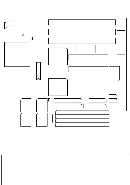
3.2. MAINBOARD LAYOUT (REV.3 and above)
J12 |
J10 |
J8 |
|
+ |
|
+ |
ISA SLOT3 |
1 |
|
|
|
J11 |
J9 |
|
|
J6 |
|
|
|
J7 |
S1 |
|
|
ISA SLOT2 |
|||
|
|
|
|
|
|||
|
|
|
|
J5 |
|
USB |
J3 |
|
123456 |
|
|
||||
|
|
|
|
|
|
||
|
|
|
|
|
|
|
|
1+
ISA SLOT1
BIOS RTC
CPU
PCI4
U10
PCI3
GA-586ATV
|
|
|
|
|
|
|
PCI2 |
|
|
|
|
|
|
|
|
|
|
|
|
|
|
|
|
|
|
|
|
|
|
|
|
|
|
|
|
|
|
|
|
|
|
|
|
|
|
|
|
|
|
|
|
|
|
|
|
|
|
PCI1 |
|
|
COMA |
|
|
|
|
||
|
|
|
|
|
|
|
|
|
|
|
CN2 |
|||||
|
|
|
J4 |
CN6 |
1 |
CN1 LPT PORT |
1 |
|||||||||
|
|
|
|
|
|
|
|
|
|
|||||||
|
|
|
IDE1 |
COMB |
|
CN3 |
||||||||||
|
1+ |
|
2 |
14 |
|
|||||||||||
|
|
|
|
CN4 |
|
|
|
|
|
|
|
|||||
SYNC |
82438VX |
|
|
1 |
1 |
|
|
PS/2 MOUSE |
||||||||
IDE2 |
FLOPPY |
|
|
|||||||||||||
SRAM |
2 |
2 |
|
|
|
|
|
|
J2 |
|||||||
|
|
|
CN7 |
|
|
|
|
|
1 |
|||||||
|
|
SIMM4 |
|
|
|
|
|
|
|
|
|
|||||
|
|
|
|
|
|
|
|
|
|
|
|
|
|
|
|
|
|
|
|
|
|
|
|
|
|
|
|
|
|
|
|
|
|
|
|
|
|
|
|
|
|
|
|
|
|
|
|
|
J1 |
|
SYNC |
82438VX |
|
|
|
|
|
|
|
|
|
|
|
|
|
||
|
|
|
|
|
|
|
|
|
|
|
Keyboard |
|||||
SRAM |
|
|
SIMM1 |
|
|
|
|
|
|
|
|
|
|
|
|
|
|
|
|
|
|
|
|
|
|
|
|
|
|
|
|
|
|
|
|
|
|
|
|
|
|
|
|
|
Power1 |
|
|
|
|
|
×Figure 3.1Ø
3.3. QUICK REFERENCE FOR JUMPERS & CONNECTORS
t J1: Keyboard Connector
|
Pin No. |
Function |
|
1 |
Key Clock. |
|
2 |
Key Data. |
|
3 |
NC. |
|
4 |
VCC (+5V). |
5 |
GND. |
|
|
|
|
|
|
3-2 |

Hardware Installation
t J2: PS/2 Mouse Connector
Pin No. |
Function |
1 |
VCC. |
2 |
GND. |
3 |
MS-DATA. |
4 |
MS-CLOCK. |
|
|
t J4: IDE Hard Disk Active LED |
|
Pin No. |
Function |
1 |
LED anode (+). |
2 |
LED cathode (-). |
|
|
t J5: CPU Cooling Fan Power Connector |
|
Pin No. |
Function |
1 |
+12V |
2 |
GND |
|
|
t J6: Speaker Connector |
|
Pin No. |
Function |
1 |
VCC. |
2 |
NC. |
3 |
NC. |
4 |
Data. |
tJ7: Power LED and Key-Lock Connector
Pin No. |
Function |
1LED anode (+).
2NC.
3LED cathode (-).
4Key lock.
5GND.
tJ8: Green Function Switch
Pin No. |
Function |
Close |
For system entering Green mode ( Suspend mode). |
Open |
Normal operation. |
tJ9: Green Function LED
Pin No. |
Function |
1LED anode (+).
2LED cathode (-).
tJ10: Reset Switch
3-3
GA-586ATV
Open |
For normal operation. |
Close |
For hardware reset system. |
tJ11: Turbo Switch
Pin No. |
Function |
Close |
For low speed (Non-cache). |
Open |
For high speed. |
tJ12: Turbo LED Connector
Pin No. |
Function |
1LED anode (+).
2LED cathode (-).
t S1-1,2: CPU BUS CLOCK
MHz |
1 |
|
|
|
2 |
|
75 |
|
OFF |
|
|
OFF |
|
66 |
|
OFF |
|
|
ON |
|
60 |
|
ON |
|
|
OFF |
|
50 |
|
ON |
|
|
ON |
|
|
|
|
|
|
|
|
t S1-3,4: CPU INT. / EXT. CLOCK RATIO¡ For] REV.3x¡ ^ |
|
|||||
|
|
|
|
|
|
|
RATIO |
3 |
|
|
|
4 |
|
x 1.5 or x 3.5 |
OFF |
|
|
OFF |
||
x 2 |
OFF |
|
|
ON |
||
x 2.5 |
ON |
|
|
ON |
||
x 3 |
ON |
|
|
OFF |
||
|
|
|
|
|
||
t S1-3, 4, 6: CPU INT. / EXT. CLOCK RATIO¡ |
For] REV.4x¡ |
^ |
||||
RATIO |
|
3 |
|
4 |
|
6 |
x 1.5 or x 3.5 |
|
OFF |
|
OFF |
OFF |
|
x 2 |
|
OFF |
|
ON |
OFF |
|
x 2.5 |
|
ON |
|
ON |
OFF |
|
x 3 |
|
ON |
|
OFF |
OFF |
|
x 5.5 |
|
OFF |
|
OFF |
ON |
|
x 4 |
|
OFF |
|
ON |
ON |
|
x 4.5 |
|
ON |
|
ON |
ON |
|
x 5 |
|
ON |
|
OFF |
ON |
|
t S1-5: AMD K6 3.2V CPU support
|
CPU |
|
5 |
|
AMD K6 3.2V CPU |
|
OFF |
|
Intel & Cyrix & AMD K5, K6 (2.9V) |
|
ON |
|
|
|
|
|
t CN1-4,6,7,J3 I/O Ports Connector |
|
|
|
|
|
|
3-4 |
|
||

Hardware Installation
CN2 |
|
For COM A (Serial port1) |
|
CN3 |
|
For COM B (Serial port2) |
|
CN4 |
|
For Floppy port |
|
CN1 |
|
For LPT port |
|
CN6 |
|
For Primary IDE port |
|
CN7 |
|
For Secondary IDE port |
|
J3 |
|
For Extended USB cable. |
|
|
|
||
t Power Connector |
|||
Pin No. |
|
Function |
|
1 |
|
|
Power Good signal |
2,10,11,12 |
|
VCC (+5V) |
|
3 |
|
|
+12V |
4 |
|
|
-12V |
5,6,7,8 |
|
|
GND |
9 |
|
|
-5V |
3.4. DRAM INSTALLATION
The mainboard can be installed with 4 / 8 / 16 / 32 MB 72 pins SIMM module DRAM, and the DRAM speed must be 60 or 70 ns. The DRAM memory system on mainboard consists of bank 0 & bank 1.
Each bank consist of 2 PCs 72 pins SIMM module DRAM. Because the 72 pins SIMM module is 32 bits width, using 2 PCs which can match a 64 bits system. The total memory size is 8 - 128 MB, and various configuration of DRAM types in the following TABLE are for reference:
BANK0 |
BANK1 |
TOTAL SIZE |
4MB * 2pcs. |
|
8MB |
4MB * 2pcs. |
4MB * 2pcs. |
16MB |
8MB * 2pcs. |
|
16MB |
8MB * 2pcs. |
4MB * 2pcs. |
24MB |
8MB * 2pcs. |
8MB * 2pcs. |
32MB |
16MB * 2pcs. |
|
32MB |
16MB * 2pcs. |
4MB * 2pcs. |
40MB |
16MB * 2pcs. |
8MB * 2pcs. |
48MB |
16MB * 2pcs. |
16MB * 2pcs. |
64MB |
32MB * 2pcs. |
|
64MB |
32MB * 2pcs. |
4MB * 2pcs. |
72MB |
32MB * 2pcs. |
8MB * 2pcs. |
80MB |
32MB * 2pcs. |
16MB * 2pcs. |
96MB |
32MB * 2pcs. |
32MB * 2pcs. |
128MB |
The DRAM installation position refer to Figure 3.1, and notice the Pin 1 of
3-5

GA-586ATV
SIMM module must match with the Pin 1 of SIMM socket when the DRAM SIMM module is installed.
Insert the DRAM SIMM module into the SIMM socket at 45 degree angle. If there is a wrong direction of Pin 1, the DRAM SIMM module couldn't be inserted into socket completely.
After completely insert SIMM module into socket, then press the SIMM module in vertical direction until the left and right metal holders can keep the SIMM module standing up con-firmly.
3.5. SRAM INSTALLATION
3.5.1 Onboard Sync. SRAM (Pipe Line Burst SRAM)
Sync SRAM consists of 2 PCs Pipeline Burst 64 K x 32- 6/7 for 512KB Sync. SRAM. The TAG SRAM (U10) is 16KBx8-12.
3.6. CPU INSTALLATION AND JUMPERS SETUP
The system's speed depends on the frequency of CLOCK GENERATOR. The user can change the selection to set up the system speed to 50 MHz, 60 MHz, 66 MHz or 75 MHz for Intel 75 - 233 MHz 3.3V ~ 3.5V and 2.8V ~ 2.9V dual power plane Pentiumâ Processor.
The mainboard can use Intel Pentiumâ Processor (MMX or PODP), Cyrix 6x86 and AMD K5 / K6 processor and the CPU speed must match with the frequency of CLOCK GEN. It will cause system hanging up if the CLOCK GEN.'S frequency is higher than CPU's.
MThe CPU is a sensitive electric component and it can be easily damaged by static electricity, so users must keep it away from metal surface when the CPU is installed onto mainboard.
MWhen the user installs the CPU on socket, please notice the PIN 1 of CPU is in the same corner as the PIN 1 of socket!
MBefore the CPU is installed, the mainboard must be placed on a flat plane in order to avoid being broken by the pressure of CPU installation.
3.7. CMOS RTC & ISA CFG CMOS SRAM
3-6
Hardware Installation
There're RTC & CMOS SRAM on board, they have a power supply from internal battery to keep the DATA inviolate & effective. The RTC is a REALTIME CLOCK device which provides the DATE & TIME to system. The CMOS SRAM is used for keeping the information of ISA device system configuration, so the system can automatically boot OS. every time.
Due to the life-time of 3V Li-battery is 5 years, the user can change a new one to replace old one after it can not work.
3.8. SPEAKER CONNECTOR INSTALLATION
There is always a speaker in AT system for sound purpose. The 4-Pins connector J6 is used to connect speaker.
The speaker can work well in both direction of connector when it is installed to the connector J6 on mainboard.
3.9. POWER LED & KEY LOCK CONNECTOR INSTALLATION
There are a system power LED lamp and a key on the panel of case. The power LED will light on when system is powered-on, and the key can lock the keyboard input or unlock it, both of them are connected to a 5 PIN connector. The connector should be installed to J7 of mainboard in correct direction.
3.10. TURBO SWITCH CONNECTOR INSTALLATION
The TURBO switch on the panel is used for controlling the system speed. Some program developed on XT should be executed with a low speed system, so a high speed system needs the speed switching function to change its running speed.
The mainboard uses 50 MHz speed method to implement DE-TURBO switching function. The J11 on mainboard should be connected to the TURBO switch on panel, and user can push in or pop out the TURBO switch to enable or disable the turbo function of system.
NOTE: If the system already use 50MHz clock, then the TURBO function will inactive.
3.11. TURBO LED CONNECTOR INSTALLATION
The TURBO LED on panel can indicate the current speed status of system. The TURBO LED connector should be installed to J12 in correct direction.
3.12. HARDWARE RESET SWITCH CONNECTOR INSTALLATION
3-7
 Loading...