

Ver. 1
SERVICE MANUAL
MODEL JP E3 E2 EK E2A E2C E1K EUT
DN-V500BD
3
BLU-RAY DISC/DVD VIDEO PLAYER
●
For purposes of improvement, specifications and design are subject to change without notice.
●
Please use this service manual with referring to the operating instructions without fail.
●
Some illustrations using in this service manual are slightly different from the actual set.
PROFESSIONAL BUSINESS COMPANY
X0460 V.01 DE/CDM 0909

SAFETY PRECAUTIONS
The following check should be performed for the continued protection of the customer and service technician.
LEAKAGE CURRENT CHECK
Before returning the unit to the customer, make sure you make either (1) a leakage current check or (2) a line to chassis
resistance check. if the leakage current exceeds 0.5 milliamps, or if the resistance from chassis to either side of the power
cord is less than 460 kohms, the unit is defective.
LASER RADIATON
Caition - Class 1M visible and invisible laser radiation when open.
Do not view directly optical instruments.
CAUTION
Heed the cautions!
◎
Spots requiring particular attention when servicing, such
as the cabinet, parts, chassis,etc., have cautions indicated
on labels. be sure to heed these causions and the cautions
indicated in the handling instructions.
Caution concerning electric shock!
◎
(1) An AC voltage is impressed on this set, so touching
internal metal parts when the set is energized could
cause electric shock. Take care to avoid electric
shock, by for example using an isolating transformer
and gloves when servicing while the set is energized,
unplugging the power cord when replacing parts, etc.
(2) Tere are high voltage parts inside. Handle with extra
care when the set is energized.
Caution concerning disassembly and
◎
Please heed he points listed below during servicing and inspection.
assembly!
Through great care is taken when manufacturing parts
from sheet metal, there may in some rare cases be burrs
RQWKHHGJHVRISDUWVZKLFKFRXOGFDXVHLQMXU\LI¿QJHUV
are moved across them. Use gloves to protect your hands.
Only use designated parts!
◎
The set's parts have specific safety properties (fire
resistance, voltage resistance, etc.). For replacement parts,
be sure to use parts which have the same poroperties. In
particular, for the important safety parts that are marked
on wiring diagrams and parts lists, be sure to use the
z
designated parts.
Be sure to mount parts and arrange the wires
◎
as they were originally!
For safety seasons, some parts use tape, tubes or other
insulating materials, and some parts are mounted away
from the surface of printed circuit boards. Care is also
taken with the positions of the wores omsode amd clamps
are used to keep wires away from heating and high voltage
parts, so be sure to set everything back as it was originally.
Inspect for safety after servicing!
◎
Check that all screws, parts and wires removed or
disconnected for servicing have been put back in their
original positions, inspect that no parts around the area that
has been serviced have been negatively affected, conduct
an inslation check on the external metal connectors and
between the blades of the power plug, and otherwise
check that safety is ensured.
(Insulation check procedure)
Unplug the power cord from the power outlet, disconnect
the antenna, plugs, etc., and turn the power switch on.
Using a 500V insulation resistance tester, check that the
inplug and the externally exposed metal parts (antenna
terminal, headphones terminal, input terminal, etc.) is
0ȍRUJUHDWHU,ILWLVOHVVWKHVHWPXVW EHLQVSHFWHGDQG
repaired.
CAUTION
Concerning important safety
parts
Many of the electric and structural parts used in the set
have special safety properties. In most cases these
properties are difficult to distinguish by sight, and using
replacement parts with higher ratings (rated power and
withstand voltage) does not necessarily guarantee that
safety performance will be poreserved. Parts with safety
properties are indicated as shown below on the wiring
diagrams and parts lists is this service manual. Be sure to
replace them with parts with the designated part number.
(1) Schematic diagrams ......Indicated by the zmark.
(2) Parts lists ......Indicated by the z mark.
Using parts other than the designated
SDUWVFRXOGUHVXOWLQ HOHFWULF VKRFN ¿UHV
or other dangerous situations.
2
DN-V500BD
%JNFOTJPO
3
DN-V500BD
WIRE ARRANGEMENT
If wire bundles are untied or moved to perform adjustment or parts replacement etc., be sure to rearrange them neatly
as they were originally bundled or placed afterward.
Otherwise, incorrect arrangement can be a cause of noise generation.
Wire arrangement viewed from the top
4
DN-V500BD
SPECIFICATIONS
5
DN-V500BD
(Standby:0.8W,Powersaving:0.75W)
4.8kg(10.6lbs)
6
DN-V500BD
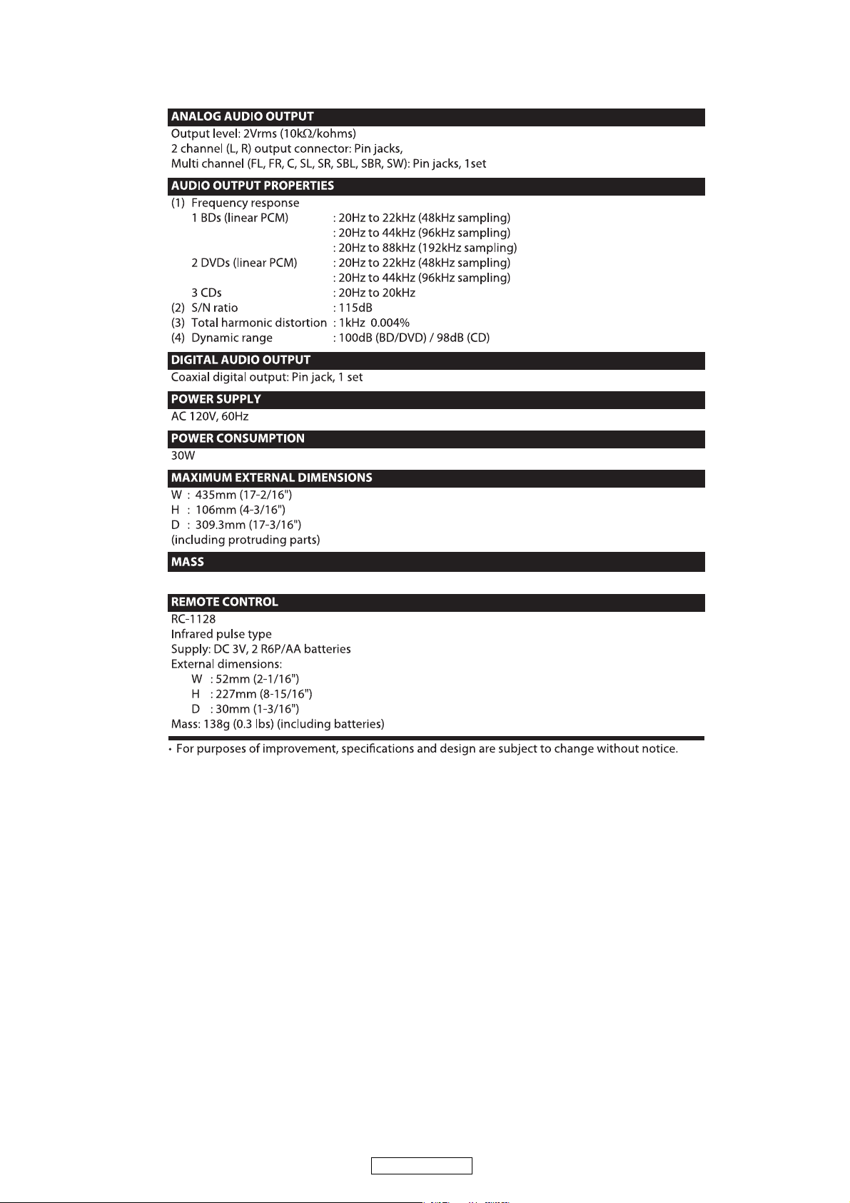
LASER BEAM SAFETY PRECAUTIONS
This BD player uses a pickup that emits a laser beam.
Do not look directly at the laser beam coming
from the pickup or allow it to strike against your
skin.
The laser beam is emitted from the location shown in the figure. When checking the laser diode, be sure to keep
your eyes at least 30 cm away from the pickup lens when the diode is turned on. Do not look directly at the laser
beam.
CAUTION: Use of controls and adjustments, or doing procedures other than those specified herein, may result in
hazardous radiation exposure.
Drive Mechanism Assembly
Laser Beam Radiation
Laser Pickup
Turntable
Location: Inside Top of BD mechanism.
7
DN-V500BD
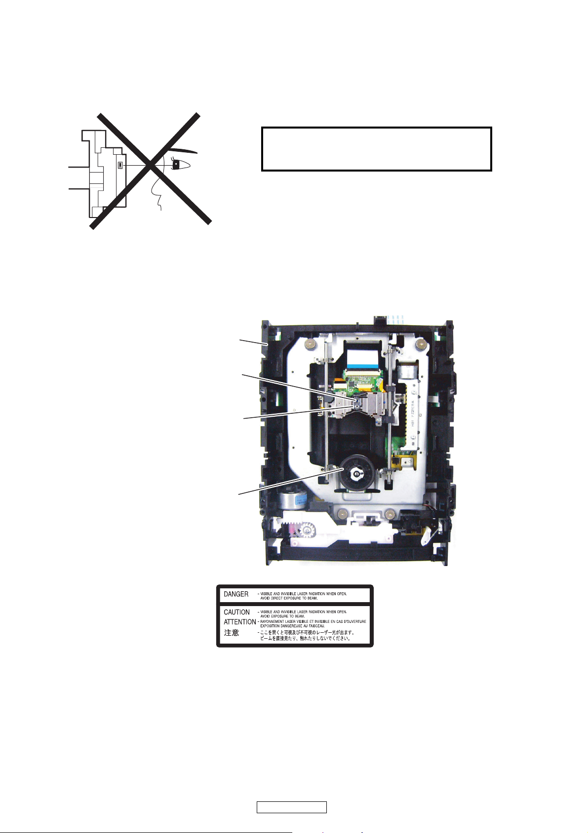
Safety Check after Servicing
Examine the area surrounding the repaired location for damage or deterioration. Observe that screws, parts, and
wires have been returned to their original positions. Afterwards, do the following tests and confirm the specified
values to verify compliance with safety standards.
1. Clearance Distance
When replacing primary circuit components, confirm
specified clearance distance (d) and (d’) between
soldered terminals, and between terminals and
surrounding metallic parts. (See Fig. 1)
Table 1: Ratings for selected area
Chassis or Secondary Conductor
Primary Circuit
AC Line Voltage Clearance Distance (d), (d’)
t
120 V
Note: This table is unofficial and for reference only. Be
sure to confirm the precise values.
3mm(d)
t
4mm(d’)
2. Leakage Current Test
Confirm the specified (or lower) leakage current
between B (earth ground, power cord plug prongs) and
externally exposed accessible parts (RF terminals,
antenna terminals, video and audio input and output
terminals, microphone jacks, earphone jacks, etc.) is
lower than or equal to the specified value in the table
below.
Measuring Method (Power ON):
Insert load Z between B (earth ground, power cord plug
prongs) and exposed accessible parts. Use an AC
voltmeter to measure across the terminals of load Z.
See Fig. 2 and the following table.
d' d
Exposed Accessible Part
Z
One side of
B
Power Cord Plug Prongs
Fig. 1
AC Voltmeter
(High Impedance)
Table 2: Leakage current ratings for selected areas
AC Line Voltage Load Z Leakage Current (i)
2k:RES.
Connected in
parallel
120 V
50k: RES.
Connected in
parallel
Note:This table is unofficial and for reference only. Be sure to confirm the precise values.
id0.7mA AC Peak
id2mA DC
id0.7mA AC Peak
id2mA DC
One side of power cord plug
prongs (B) to:
RF or
Antenna terminals
A/V Input, Output
8
DN-V500BD
Fig. 2
STANDARD NOTES FOR SERVICING
Circuit Board Indications
1. The output pin of the 3 pin Regulator ICs is
indicated as shown.
Top View
Out
2. For other ICs, pin 1 and every fifth pin are
indicated as shown.
Pin 1
3. The 1st pin of every male connector is indicated as
shown.
Pin 1
Input
In
Bottom View
5
10
Pb (Lead) Free Solder
When soldering, be sure to use the Pb free solder.
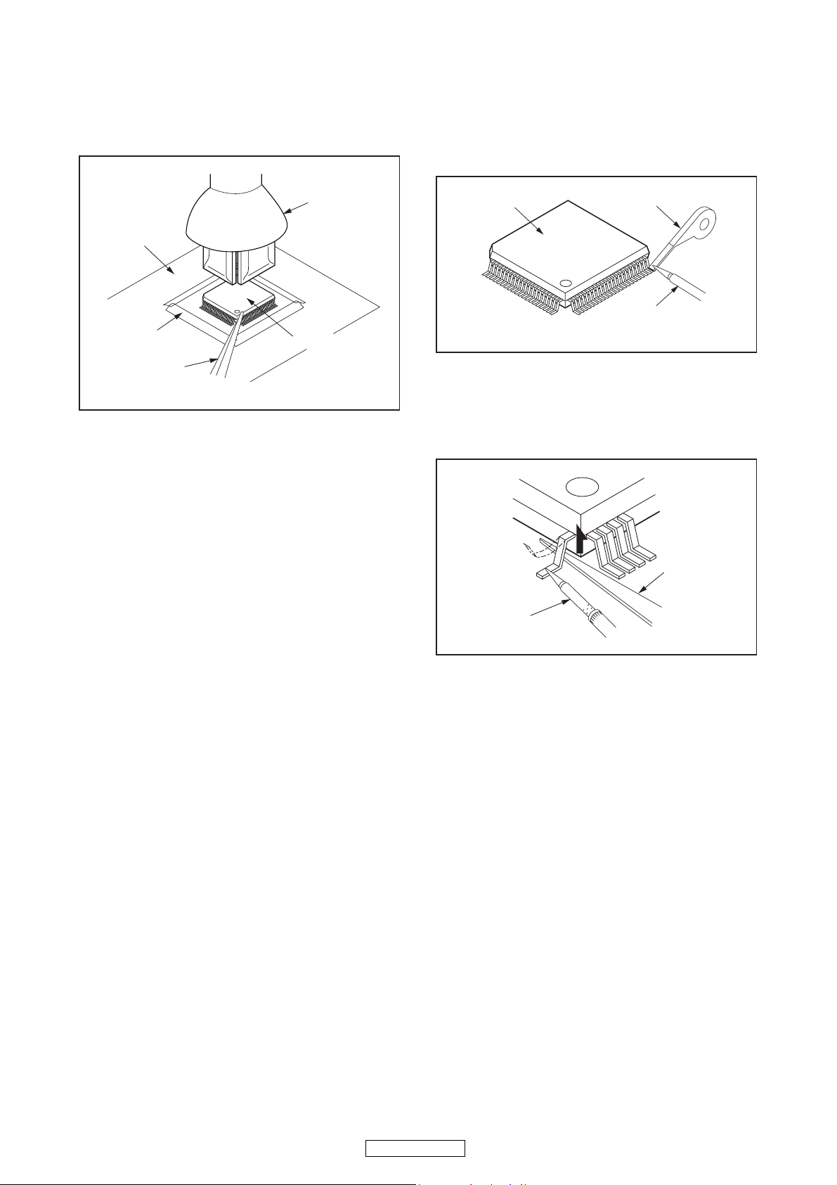
How to Remove / Install Flat Pack-IC
1. Removal
With Hot-Air Flat Pack-IC Desoldering Machine:
1. Prepare the hot-air flat pack-IC desoldering
machine, then apply hot air to the Flat Pack-IC
(about 5 to 6 seconds). (Fig. S-1-1)
Fig. S-1-1
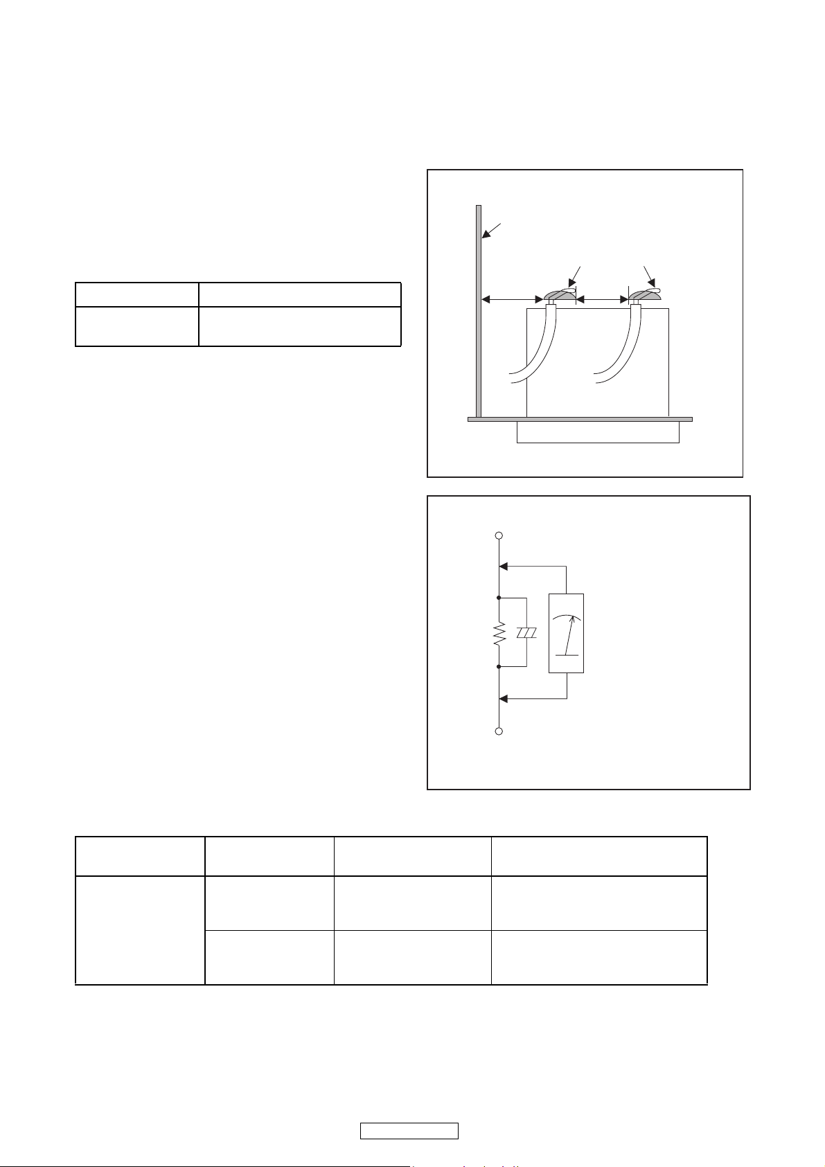
Instructions for Connectors
1. When you connect or disconnect the FFC (Flexible
Foil Connector) cable, be sure to first disconnect
the AC cord.
2. FFC (Flexible Foil Connector) cable should be
inserted parallel into the connector, not at an
angle.
FFC Cable
Connector
CBA
* Be careful to avoid a short circuit.
2. Remove the flat pack-IC with tweezers while
applying the hot air.
3. Bottom of the flat pack-IC is fixed with glue to the
CBA; when removing entire flat pack-IC, first apply
soldering iron to center of the flat pack-IC and heat
up. Then remove (glue will be melted). (Fig. S-1-6)
4. Release the flat pack-IC from the CBA using
tweezers. (Fig. S-1-6)
CAUTION:
1. The Flat Pack-IC shape may differ by models. Use
an appropriate hot-air flat pack-IC desoldering
machine, whose shape matches that of the Flat
Pack-IC.
2. Do not supply hot air to the chip parts around the
flat pack-IC for over 6 seconds because damage
to the chip parts may occur. Put masking tape
around the flat pack-IC to protect other parts from
damage. (Fig. S-1-2)
9
DN-V500BD
3. The flat pack-IC on the CBA is affixed with glue, so
be careful not to break or damage the foil of each
pin or the solder lands under the IC when
removing it.
With Soldering Iron:
1. Using desoldering braid, remove the solder from
all pins of the flat pack-IC. When you use solder
flux which is applied to all pins of the flat pack-IC,
you can remove it easily. (Fig. S-1-3)
CBA
Masking
Tape
Tweezers
Hot-air
Flat Pack-IC
Desoldering
Machine
Flat Pack-IC
Fig. S-1-2
Flat Pack-IC
2. Lift each lead of the flat pack-IC upward one by
one, using a sharp pin or wire to which solder will
not adhere (iron wire). When heating the pins, use
a fine tip soldering iron or a hot air desoldering
machine. (Fig. S-1-4)
Desoldering Braid
Soldering Iron
Fig. S-1-3
Sharp
Pin
Fine Tip
Soldering Iron
3. Bottom of the flat pack-IC is fixed with glue to the
CBA; when removing entire flat pack-IC, first apply
soldering iron to center of the flat pack-IC and heat
up. Then remove (glue will be melted). (Fig. S-1-6)
4. Release the flat pack-IC from the CBA using
tweezers. (Fig. S-1-6)
Fig. S-1-4
10
DN-V500BD
With Iron Wire:
1. Using desoldering braid, remove the solder from
all pins of the flat pack-IC. When you use solder
flux which is applied to all pins of the flat pack-IC,
you can remove it easily. (Fig. S-1-3)
2. Affix the wire to a workbench or solid mounting
point, as shown in Fig. S-1-5.
3. While heating the pins using a fine tip soldering
iron or hot air blower, pull up the wire as the solder
melts so as to lift the IC leads from the CBA
contact pads as shown in Fig. S-1-5.
4. Bottom of the flat pack-IC is fixed with glue to the
CBA; when removing entire flat pack-IC, first apply
soldering iron to center of the flat pack-IC and heat
up. Then remove (glue will be melted). (Fig. S-1-6)
5. Release the flat pack-IC from the CBA using
tweezers. (Fig. S-1-6)
Note: When using a soldering iron, care must be
taken to ensure that the flat pack-IC is not
being held by glue. When the flat pack-IC is
removed from the CBA, handle it gently
because it may be damaged if force is applied.
Hot Air Blower
2. Installation
1. Using desoldering braid, remove the solder from
the foil of each pin of the flat pack-IC on the CBA
so you can install a replacement flat pack-IC more
easily.
2. The “●” mark on the flat pack-IC indicates pin 1.
(See Fig. S-1-7.) Be sure this mark matches the
pin 1 on the PCB when positioning for installation.
Then presolder the four corners of the flat pack-IC.
(See Fig. S-1-8.)
3. Solder all pins of the flat pack-IC. Be sure that
none of the pins have solder bridges.
Example :
Pin 1 of the Flat Pack-IC
is indicated by a " " mark.
Fig. S-1-7
To Solid
Mounting Point
CBA
Tweezers
Iron Wire
Soldering Iron
Fig. S-1-5
Fine Tip
Soldering Iron
Flat Pack-IC
or
Presolder
Flat Pack-IC
CBA
Fig. S-1-8
Fig. S-1-6
DN-V500BD
11
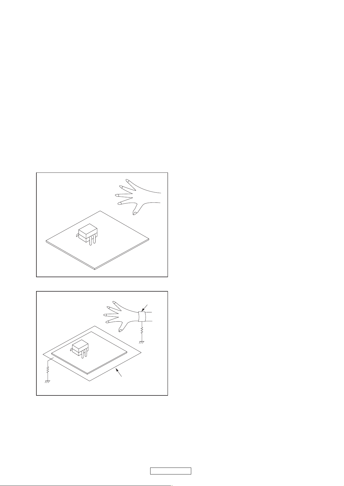
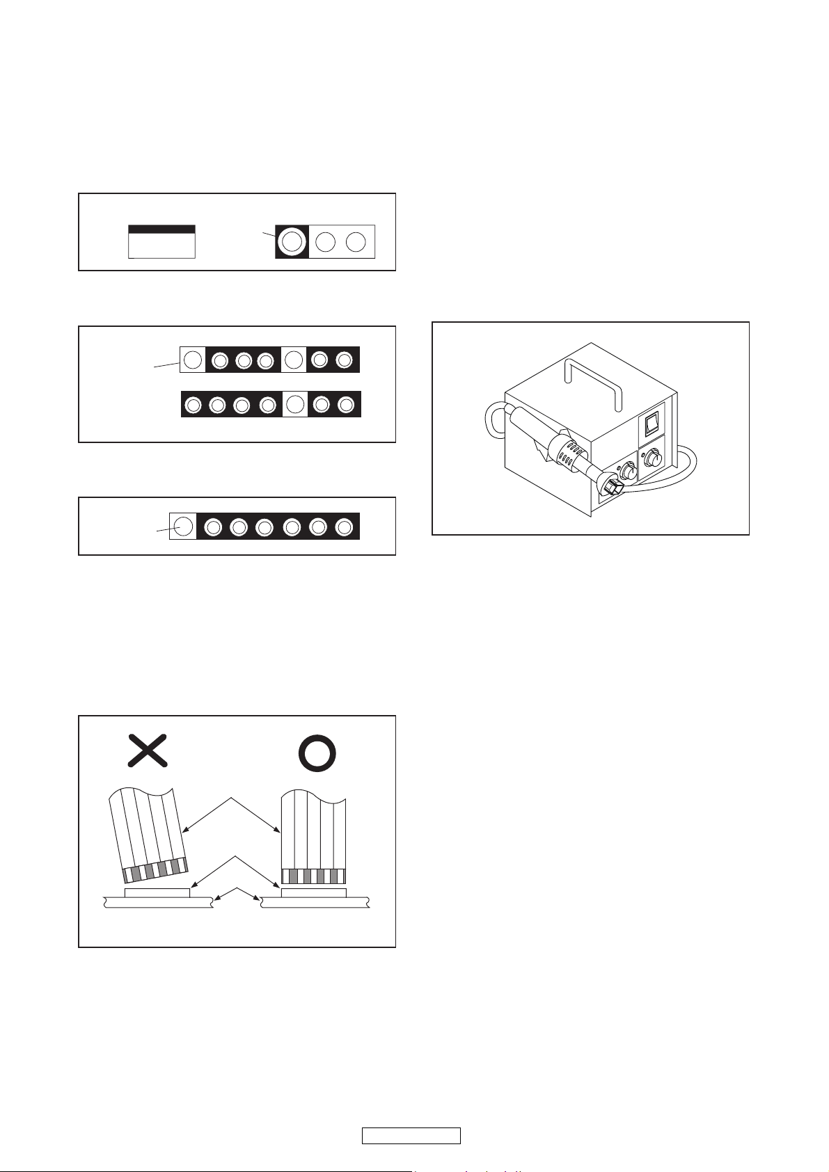
Instructions for Handling Semiconductors
Electrostatic breakdown of the semi-conductors may
occur due to a potential difference caused by
electrostatic charge during unpacking or repair work.
1. Ground for Human Body
Be sure to wear a grounding band (1 M:) that is
properly grounded to remove any static electricity that
may be charged on the body.
2. Ground for Workbench
Be sure to place a conductive sheet or copper plate
with proper grounding (1 M:) on the workbench or
other surface, where the semi-conductors are to be
placed. Because the static electricity charge on
clothing will not escape through the body grounding
band, be careful to avoid contacting semi-conductors
with your clothing.
<Incorrect>
<Correct>
1MΩ
CBA
Grounding Band
1MΩ
CBA
Conductive Sheet or
Copper Plate
12
DN-V500BD
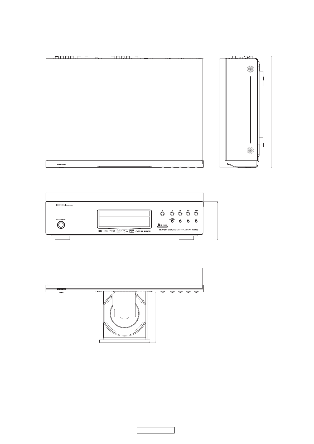
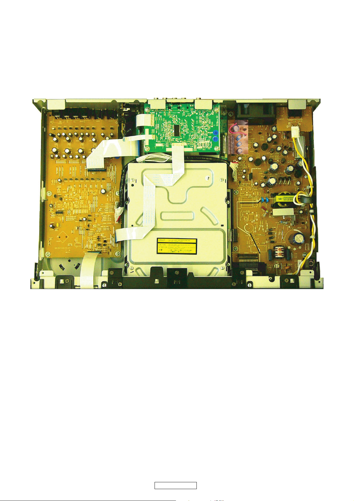
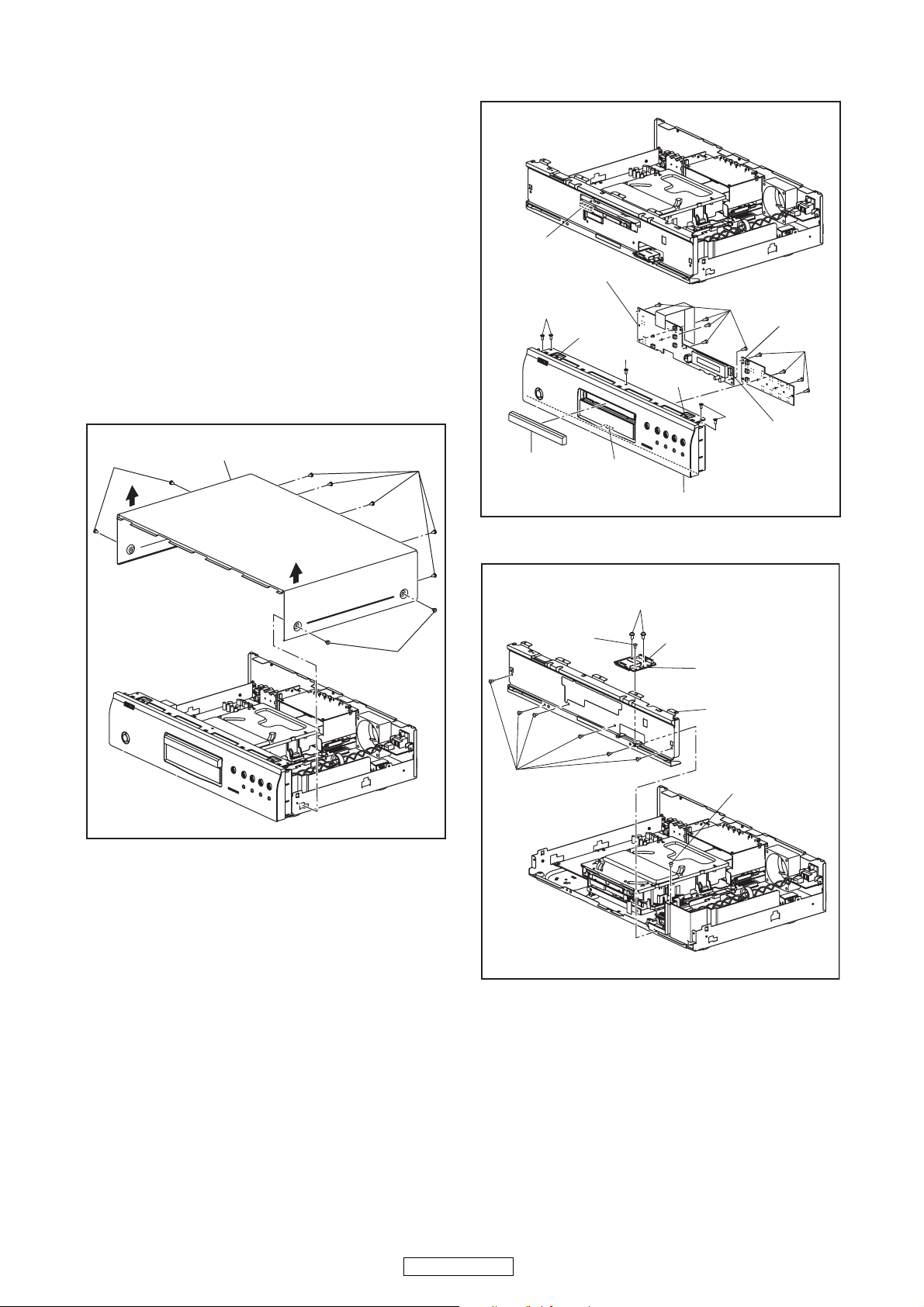
CABINET DISASSEMBLY INSTRUCTIONS
1. Disassembly Flowchart
This flowchart indicates the disassembly steps to gain
access to item(s) to be serviced. When reassembling,
follow the steps in reverse order. Bend, route, and
dress the cables as they were originally.
[1] Top Cover
[2] Tray Panel
[5] Front B CBA
[11] RS232C
CBA
[12] Audio CBA
[3] Front
Assembly
[6] Front Bracket
[8] Rear Panel
[13] Video CBA
[14] AV PCB
Bracket
[15] BD Main CBA
& BD Mechanism
Assembly
[16] Loader
Bracket
[4] Front A CBA
[9] Motor
DC Fan
[10] Inlet CBA
[7] SD CBA
[17] Power
Supply CBA
[18] Power
Holder
2. Disassembly Method
ID/
Loc.
No.
Part
Fig.
No.
[1] Top Cover D1 9(S-1) ---
[2] Tray Panel D2 --------------- 1
[3]
[4]
[5]
[6]
[7]
Front
Assembly
Front A
CBA
Front B
CBA
Front
Bracket
SD CBA
*2(L-1), *(L-2), 5(S-2),
D2
9(S-3), *CN2002
D2 *CN3001 ---
D2 --------------- ---
D3 7(S-4), (S-5) ---
D3 2(S-6), *CN5001 ---
5(S-7), (S-8), 2(S-9),
[8] Rear Panel D4
(S-10), (S-11),
11(S-12), 2(S-13),
2(S-14), *CN1006
Motor DC
[9]
Fan
D4 --------------- ---
Removal
Remove/*Unhook/
Unlock/Release/
Unplug/Desolder
Note
2
---
ID/
Loc.
No.
[10]
[11]
Part
Inlet CBA
RS232C
CBA
Fig.
No.
D4 *CN1001 ---
D4 *CN5501
[12] Audio CBA D5
5(S-15), *CN2005,
*CN2007, *CN2008
Removal
Remove/*Unhook/
Unlock/Release/
Unplug/Desolder
Note
---
[13] Video CBA D6 4(S-16), *CN7101 ---
AV PCB
[14]
Bracket
D6 4(S-17) ---
BD Main
[15]
CBA & BD
Mechanism
4(S-18), *CN6001,
D6
*CN7601
Assembly
Loader
[16]
Bracket
D6 6(S-19)---
Power
[17]
Supply
D7 3(S-20), 2(S-21) ---
CBA
Power
[18]
p
(1)
Holder
p
(2)
D7 3(S-22) ---
p
(3)
p
(4)
(5)
Note:
(1) Identification (location) No. of parts in the figures
(2) Name of the part
(3) Figure Number for reference
(4) Identification of parts to be removed, unhooked,
unlocked, released, unplugged, unclamped, or
desoldered.
P = Spring, L = Locking Tab, S = Screw,
CN = Connector
* = Unhook, Unlock, Release, Unplug, or Desolder
e.g. 2(S-2) = two Screws (S-2),
2(L-2) = two Locking Tabs (L-2)
(5) Refer to “Reference Notes.”
About tightening screws
When tightening screws, tighten them with the
following torque.
Torque
0.45 ± 0.05 N·m
3
p
13
DN-V500BD
Reference Note
1. How to remove tray panel
1) Connect the wall plug to an AC outlet and press
the [ A] button to open the tray.
2) To lift up, the tray panel is removed.
3) Press the [ A] button again to close the tray.
4) Press the [ON/STANDBY] button to turn the
power off.
5) Unplug an AC cord.
2. CAUTION 1: Locking Tabs (L-1) and (L-2) are
fragile. Be careful not to break them.
3. The BD Main CBA & BD Mechanism Assembly
is adjusted as a unit at factory. Therefore, do
not disassemble it. Replace the BD Main CBA
& BD Mechanism Assembly as a unit.
(S-1)
[1] Top Cover
(S-1)
CN2002
[4] Front A CBA
(S-2)
(L-1)
[2] Tray Panel
(S-2)
(L-2)
(L-1)
(S-3)
(S-2)
[5] Front B
CBA
(S-3)
CN3001
(S-1)
Fig. D1
(S-4)
(S-5)
[3] Front Assembly
(S-6)
CN5001
[7] SD CBA
[6] Front Bracket
(S-4)
Fig. D2
14
DN-V500BD
Fig. D3
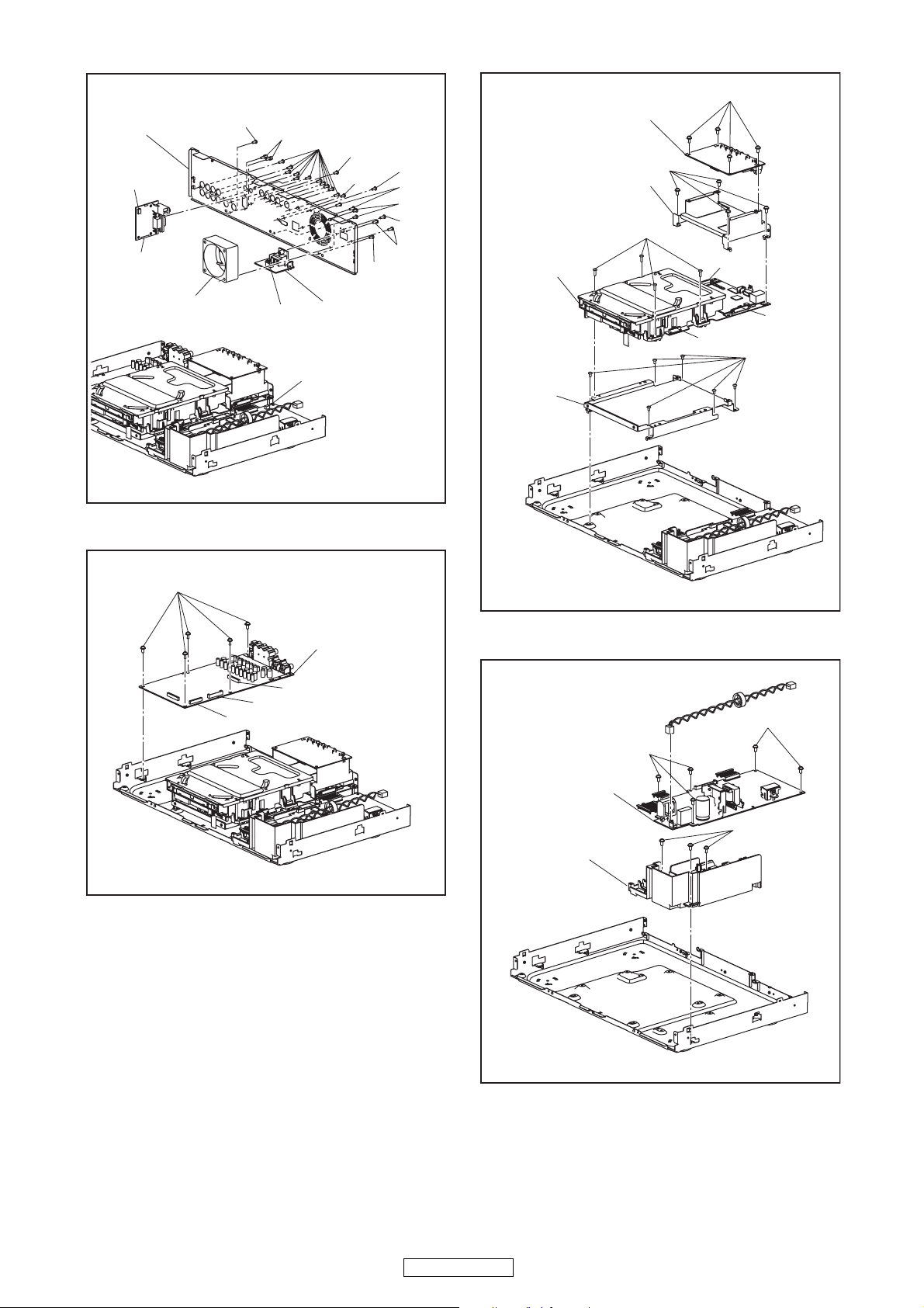
(S-16)
[8] Rear Panel
CN5501
[11] RS232C
CBA
[9] Motor DC Fan
(S-7)
(S-13)
CN1001
(S-12)
(S-7)
(S-11)
(S-7)
[10] Inlet CBA
CN1006
(S-10)
(S-14)
(S-7)
(S-8)
(S-9)
Fig. D4
[13] Video CBA
[14] AV PCB Bracket
[15] *BD Main CBA
& BD Mechanism
Assembly
[16] Loader
Bracket
(S-17)
(S-18)
CN7101
CN6001
CN7601
(S-19)
(S-15)
CN2008
CN2005
[12] Audio CBA
CN2007
Fig. D5
* See Reference Notes 3.
(S-20)
[17] Power Supply
CBA
[18] Power Holder
Fig. D6
(S-21)
(S-22)
15
DN-V500BD
Fig. D7
3. How to Eject Manually
1. Remove the Top Cover.
2. Insert a screwdriver, etc. into the straightly so that the Portion A is pushed.
3. Pull the tray out manually and remove a disc.
Portion A
Screwdriver,
hexagon wrench
16
DN-V500BD

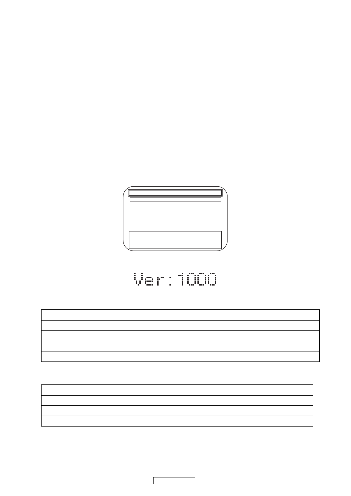
HOW TO INITIALIZE THE BLU-RAY DISC PLAYER
To put the program back at the factory-default,
initialize the BD player as the following procedure.
1. Turn the power on.
2. Remove the disc on the tray and close the tray.
3. Press [1], [2], [3], [4], and [DISPLAY] buttons on
the remote control unit in that order.
Fig. a appears on the screen.
"
" differ depending on the models.
*******
Version Info
F/W Name
Version
Region
: *******
: *.***
: *-*
EXIT <POWER>EEPROM CLEAR <STOP>
Fig. a
4. Press [ C ] button on the remote control unit.
Fig. b appears on the screen and Fig. c appears
on the VFD.
"
" differ depending on the models.
*******
Version Info
F/W Name
Version
Region
EEPROM CLEAR : OK
: *******
: *.***
: *-*
EXIT <POWER>EEPROM CLEAR <STOP>
Fig. b
Fig. c
5. To exit this mode, press [POWER OFF] button.
17
DN-V500BD
FIRMWARE RENEWAL MODE
Note: The file extension of the available firmware is
“b20”.
1. Turn the power on and remove the disc on the tray
and close the tray.
2. To put the BD player into version up mode, press
[9], [8], [7], [6], and [POP UP MENU/MENU]
buttons on the remote control unit in that order.
The tray will open automatically.
Fig. a appears on the screen and Fig. b appears
on the VFD.
"
" differs depending on the models.
*******
F/W VERSION UP MODE F/W Name: ******* Ver. *.***
Please insert a Disc
for F/W Version Up
Fig. a Version Up Mode Screen
Fig. b VFD in Version Up Mode
3. Load the disc for version up.
4. The BD player enters the F/W version up mode
automatically. Fig. c appears on the screen and
Fig. d appears on the VFD. Make sure to insert the
proper F/W for the state of this model.
"
" differs depending on the models.
*******
F/W VERSION UP MODE F/W Name: ******* Ver. *.***
1. ALL
(*1)
Ver. *.*** ************A*.b20
Now Loading...
The appearance shown in (*1) of Fig. c is
described as follows:
No. Appearance State
1 Now Loading... Loading the disc
Sending files into the
2 Reading...
memory.
After reading, automatically
the tray opens.
Writing new version data,
3 See FL Display
the progress will be displayed
as shown in Fig. e.
Fig. e VFD in Vresion Up Mode
5. After programming is finished, the checksum on
the VFD (Fig. f).
Fig. f
VFD upon Finishing the Programming Mode (Example)
Checksum appears on the VFD then the tray will
open automatically. Remove the disc on the tray.
At this time, no button is available.
6. Unplug the AC cord from the AC outlet. Then plug
it again.
7. Turn the power on.
8. Press [1], [2], [3], [4], and [DISPLAY] buttons on
the remote control unit in that order.
Fig. g appears on the screen.
"
" differ depending on the models.
*******
Version Info
F/W Name
Version
Region
: *******
: *.***
: *-*
EXIT : POWER
Fig. c Programming Mode Screen (Example)
Fig. d VFD in Programming Mode (Example)
EXIT <POWER>EEPROM CLEAR <STOP>
Fig. g
18
DN-V500BD

9. Press [ C ] button on the remote control unit.
Fig. h appears on the screen and Fig. i appears on
the VFD.
"
" differ depending on the models.
*******
Version Info
F/W Name
Version
Region
EEPROM CLEAR : OK
: *******
: *.***
: *-*
EXIT <POWER>EEPROM CLEAR <STOP>
Fig. h
Fig. i
To exit this mode, press [POWER OFF] button.
19
DN-V500BD

FIRMWARE RENEWAL MODE (Network Update)
1. Press [SETUP] button on the remote control unit in
stop mode.
2. Use [
} / O] button to select “CUSTOM”, then
press [ENTER] button.
3. Use [
} / O] button to select “Other”, then press
[ENTER] button.
4. Use [
X / Y] button to select “Network Update”,
then press [ENTER] button.
Confirmation message will appear.
5. Use [
X / Y] button to select “Yes”, then press
[ENTER] button.
NOTE:
If any error message concerning the network
environment appears, please confirm the
setting of your unit according to the error
message. If you need to change any of your
network environmental setting in order to
execute the update, please contact to the
internet service provider.
6. Confirmation message will appear.
Use [
X / Y] button to select “Yes”, then press
[ENTER] button.
The unit will start downloading the latest firmware
version.
7. When the download completes, confirmation
message will appear.
Press [ENTER] button.
The unit will start updating the firmware version.
It may take a while to complete the updating.
(Please wait until “100%” appears on the front
panel display.)
8. After updating finishes, this unit will restart and
open the disc tray automatically.
How to Verify the Firmware Version
1. Turn the power on.
2. Remove the disc on the tray and close the tray.
3. Press [1], [2], [3], [4], and [DISPLAY] buttons on
the remote control unit in that order.
Fig. j appears on the screen.
"
" differ depending on the models.
*******
Version Info
F/W Name
Version
Region
4. To exit this mode, press [POWER OFF] button.
: *******
: *.***
: *-*
EXIT <POWER>EEPROM CLEAR <STOP>
Fig. j
20
DN-V500BD
SERVICE MODE
Service Mode
1st level 2nd level 3rd level Description
1 MECHA TEST
2 VFD/LED TEST
3 ERROR RATE
4 LD TEST
CHANNEL
5
TEST
6 SD CARD TEST
DEFAULT
7
SETTING
1 Tray Aging Aging of tray open/close
2 TOC Read TOC reading
3 Heat Run
1 All On Turning on all VFD
2 All Off Turning off all VFD
1 Off Turning off LD
1LD Power
2 Operating Time
1 TEST TONE
2Front Lch
3 Center
4Front Rch
5 Surround Rch
Surround Back
6
Rch
7 Surround Back Lch
8 Surround Lch
9 Sub woofer
2 BD Turning on BD LD
3 DVD Turning on DVD LD
4 CD Turning on CD LD
Center/Subwoofer/
1
Front LR
Surround LR/
2
Surround Back LR
Tray close -> TT1 playback -> TT10
playback -> Tray open -> Tray close
Displaying Error rate, Jitter
during playback
Displaying LD Operation Time (with
clear function)
Default setting
Note: If some test are performed continuously, any error will occur
21
DN-V500BD
Entering Service Mode
In power on condition, no discs and tray close, it will be entered into service mode by the following operation using
the remote controller. However, it will not be entered when Media Select Item is SD Memory.
Service Mode by using remote controller
Press the following buttons on the remote controller in power on condition, no discs and tray close;
[2]->[5]->[8]->[0]->[CLEAR]
Release from Service Mode
Press the [POWER OFF] button to turn off power.
Screen saver/Auto Power Off in Service Mode
These functions are not performed in Service Mode.
After entering, Fig. k appears on the screen and Fig. l appears on the VFD.
* Firmware Version differs depending on the
models, and this indication is one example.
SERVICE MODE
1: MECHA TEST
2: VFD/LED TEST
3: ERROR RATE MEASURE
4: LD TEST
5: CHANNEL TEST
6: SD CARD TEST
7: DEFAULT SETTING
F/W Name :******* Region
Release Ver. :*.***
ADSP1/2 Ver. :---/--- PLD Ver. :--FPGA Ver. :--- I/P Scaler Ver.:---
:*-*
Fig. k Service Mode (Main Menu)
Fig. I Service Mode
Available button in service mode
Button condition
ENTER Enter the next level
POWER Turn the power off (when the service mode is completed)
1~7 Enter the selected item (next level)
OTHER Not available
Note: Press the number key to select items. Or, press the cursor button (up/down) to select items and press
[ENTER] button.
INDICATION DESCRIPTION REMARK
F/W Name Model Name E5K***D, etc.
Region BD region - DVD region A-1, etc.
Release Ver. Release version D.jpp, etc.
22
DN-V500BD

TRAY LOCK MODE
Tray Lock Mode prevents the tray opening or closing to
prevent disc theft in demo mode.
Enter this mode using the following procedure.
1. Confirm that the TV Monitor is connected.
2. With playback stopped, press [SETUP], [TOP
MENU], [3], [AUDIO], [0] and [SETUP] buttons on
the remote control unit in that order. "Trade-On"
appears in the upper right corner on the screen,
and Fig. a appears on the VFD for 2 seconds.
Fig. a
3. To exit this mode, press [SETUP], [TOP MENU],
[3], [AUDIO], [0] and [SETUP] buttons on the
remote control unit in that order. "Trade-Off"
appears in the upper right corner on the screen,
and Fig. b appears on the VFD for 2 seconds.
Fig. b
23
DN-V500BD

REMOTE LOCK MODE
SETTING MENU:
Remote Lock Off Mode:
This mode receives an input signal from the remote
control unit or from the Remote In-Jack on the rear
panel.
Remote Lock On Mode:
This mode dose not receive an input signal from
the remote control unit or from the Remote In-Jack
on the rear panel.
Perform the setting using the following procedure.
1. Press [POWER ON] and [STOP] buttons on the
front panel simultaneously for over 3 seconds to set
"Remote Lock Mode" and display mode.
2. Press [STILL/PAUSE] button on the front panel to
set to "On" or "Off". When "Remote Lock On",
"Remote Lock On" will appear in the upper right
corner on the screen and appears on the VFD.
Fig.a VFD
When "Remote Lock Off", "Remote Lock Off" will
appear in the upper right corner on the screen and
appears on the VFD.
Fig.b VFD
a. If [STILL/PAUSE] button is not pressed for 5
seconds or any other button is pressed within 5
seconds, the unit will be released from
"Remote Lock Mode".
b. When initializing, set the Remote Lock Mode
"off".
24
DN-V500BD

FLOW CHART NO.1
The power cannot be turned on.
TROUBLESHOOTING
Is the fuse normal?
Ye s
Is normal state restored when once unplugged
power cord is plugged again after several seconds?
Ye s
Is the EV+5V line voltage normal?
Ye s
Check each rectifying circuit of the secondary circuit
and service it if defective.
FLOW CHART NO.2
The fuse blows out.
Check the presence that the primary component
is leaking or shorted and service it if defective.
After servicing, replace the fuse.
FLOW CHART NO.3
When the output voltage fluctuates.
No
No
No
See FLOW CHART No.2 <The fuse blows out.>
Check if there is any leak or short-circuiting on the
primary circuit component, and service it if defective.
(D1007, D1008, D1011, D1012, D1023, D1024,
IC1002, Q1002, T1002, C1022, R1022)
Check the presence that the rectifying diode or
circuit is shorted in each rectifying circuit of
secondary side, and service it if defective.
Does the photo coupler circuit on the secondary
side operate normally?
Ye s
Check D1021, IC1002, IC1004 and their periphery,
and service it if defective.
FLOW CHART NO.4
When buzz sound can be heard in the vicinity of power circuit.
Check if there is any short-circuit on the rectifying diode and the circuit in each rectifying circuit of the secondary
side, and service it if defective. (D1025, D1028, D1030, D1031, D1032, D1033, IC1008, IC1009, IC1010, Q1009,
Q1010, Q1011, Q1013, Q2636)
FLOW CHART NO.5
FL is not outputted.
Is 35V voltage supplied to the emitter of Q2602?
Ye s
Is the "L" signal outputted to the collector of
Q2603?
Ye s
Check Q2601, Q2602, D2603 and their periphery,
and service it if defective.
No
No
No
Check D1029, IC1004 and their periphery,
and service it if defective.
Check D1032, C1033 and periphery circuit,
and service it if defective.
Is the "H" signal inputted to the base of Q2603?
Ye s
Replace Q2603.
Check FL-SW line and service
it if defective.
No
25
DN-V500BD

FLOW CHART NO.6
P-ON+5V (1) is not outputted.
Is 5V voltage inputted to the emitter of Q1011?
Ye s
Is 4.5V voltage inputted to the base of Q1011?
Ye s
Replace Q1011.
FLOW CHART NO.7
P-ON+5V (2) is not outputted.
Is 5V voltage inputted to the emitter of Q1009?
Ye s
Is 4.5V voltage inputted to the base of Q1009?
Ye s
Replace Q1009.
FLOW CHART NO.8
P-ON+10.5V is not outputted.
Is 14V voltage inputted to the collector of Q1013?
Ye s
Is 11V voltage inputted to the base of Q1013? Is 14V voltage inputted to the base of Q1006?
Ye s Ye s No
Replace Q1013.
FLOW CHART NO.9
P-ON+1.2V is not outputted.
No
No
No
No
No
No
Check D1025, D1030, D1031, C1029, C1034 and
their periphery, and service it if defective.
Check Q1007 and PWSW4 line and service it if
defective.
Check D1025, D1030, D1031, C1029, C1034 and
their periphery, and service it if defective.
Check Q1007 and PWSW4 line and service it if
defective.
Check D1029, D1041, C1026, L1004
their periphery, and service it if defective.
Check Q1006, D1046,
and their periphery, and
service it if defective.
Check Q1008,
PWSW4 line, and
service it if defective.
and
and
Is 5V voltage supplied to Pin(3) of IC1009?
Ye s
Is the "L" signal inputted to the base of Q1015?
Ye s
Check IC1009, Q1015
service it if defective.
FLOW CHART NO.10
P-ON+3.3V is not outputted.
Is 5V voltage supplied to Pin(1) of IC1008?
ls "L" signal outputted to the collector of Q1005?
Check IC1008, D1040 and their periphery circuit,
and service it if defective.
and their periphery, and
Ye s
Ye s
No
No
No
No
Check D1025, D1030, D1031, C1029, C1034 and
their periphery, and service it if defective.
Check PWSW2 line and service it if defective.
Check D1025, D1030, D1031, C1029, C1034 and
their periphery, and service it if defective.
Check Q1005 and PWSW1 line and service it if
defective.
26
DN-V500BD

FLOW CHART NO.11
P-ON+1.8V is not outputted.
Is 5V voltage inputted to Pin(3) of IC1010?
Ye s
ls "L" signal outputted to the base of Q1016?
Ye s
Check IC1010, Q1016
service it if defective.
FLOW CHART NO.12
P-ON+14.5V is not outputted.
Is 15V voltage inputted to the emitter of Q1010?
Is 14V voltage inputted to the base of Q1010?
Replace Q1010.
FLOW CHART NO.13
The fluorescent display tube does not light up.
Is 3.3V voltage supplied to Pin(24) of FL3001?
and their periphery, and
Ye s
Ye s
No
No
No
No
No
Check D1025, D1030, D1031, C1029, C1034
and their periphery, and service it if defective.
Check PWSW2 line and their periphery, and service it
if defective.
Check D1028, C1026, L1003 and their periphery, and
service it if defective.
Check Q1008 and PWSW4 line and service it if
defective.
Check the EV+3.3V line and service it if defective.
Ye s
Is 9V voltage supplied to Pin(1,2) of FL3001?
Ye s
Is 5V voltage supplied to Pin(29,30) of FL3001?
Ye s
Replace FL3001.
FLOW CHART NO.14
The key operation is not functioning.
Are the contact point and the installation state of the key
switches (SW3001, SW3101, SW3102, SW3104, SW3106,
SW3108, SW3110-3113) normal?
Ye s
When pressing each switches (
SW3102, SW3104, SW3106, SW3108, SW3110-3113
do the voltage of Pin(1, 62) of IC2000 increase?
Replace IC2000.
SW3001, SW3101,
Ye s
No
No
No
No
),
Is 10V voltage supplied to the emitter of Q2604?
Ye s N o
Is 9V voltage inputted
to the base of Q2604?
Ye s N o
Replace Q2604.
Check the F2
Re-install the switches (
SW3104, SW3106, SW3108, SW3110-3113
replace the poor switch.
Check the switches (
SW3104, SW3106, SW3108, SW3110-3113
periphery, and service it if detective.
Check Q2603 and FL-SW
and service it if defective.
line and service it if defective.
Check D1033, C1028, R1032,
R1033 and their periphery,
and service it if defective.
line
SW3001, SW3101, SW3102,
) correctly or
SW3001, SW3101, SW3102,
) and their
27
DN-V500BD

FLOW CHART NO.15
No operation is possible from the remote control unit.(Operation is possible from the unit.)
Is 5V voltage supplied to Pin(2) of RS3001
(remote control receiver) ?
Ye s
Is the "L" pulse sent out Pin(1) of RS3001 (remote
control receiver) when the remote control unit is activated?
Ye s
Is the "L" pulse inputted to the Pin(27) of IC2000?
Ye s
Replace IC2000.
FLOW CHART NO.16
The disc tray cannot be opened and closed. (It can be done using the remote control unit.)
Is the normal control voltage inputted to Pin(62) of
IC2000?
operation is not functioning.>
Replace the BD Main CBA & BD Mechanism
Assembly.
Refer to "FLOW CHART NO.14" <The key
Ye s
No
No
No
No
Check EV+5V line and service it if defective.
Replace the RS3001 (remote control receiver) or
remote control unit.
Check the line between the
receiver)
defective.
Replace the "OPEN/CLOSE" switch (SW3101).
and the
Pin(27) of IC2000,
RS3001 (remote control
and service it if
FLOW CHART NO.17
The disc tray cannot be opened and closed.
[No Disc] indicated.
Both functions of picture and sound do not operate normally.
Ye s
Replace the BD Main CBA & BD Mechanism
Assembly.
28
DN-V500BD

FLOW CHART NO.18
Picture does not appear normally.
Set the disc on the disc tray, and playback.
Are the video signals outputted to each pin of
CN4000?
CN4000 3PIN VIDEO
CN4000 5PIN VIDEO-Y(I/P)
CN4000 7PIN VIDEO-Pb/Cb
CN4000 9PIN VIDEO-Pr/Cr
Ye s
Are the video signals shown above inputted into
each pin of IC4000?
IC4000 3PIN VIDEO
IC4000 8PIN VIDEO-Y(I/P)
IC4000 10PIN VIDEO-Pb/Cb
IC4000 12PIN VIDEO-Pr/Cr
Ye s
Are the video signals outputted to each pin of
IC4000?
IC4000 20PIN VIDEO-Y(I/P)
IC4000 17PIN VIDEO-Pb/Cb
IC4000 15PIN VIDEO-Pr/Cr
IC4000 25PIN VIDEO
Ye s
Are the video signals outputted to the specific
output terminal?
Are the component video signals outputted to the
VIDEO OUT terminal (JK4002, JK4003, JK4005)?
Are the composite video signals outputted to
the VIDEO OUT terminal (JK4004)?
No
No
No
No
No
Replace the BD
Assembly.
Check the line between each pin of CN4000 and
each pin of IC4000, and service it if defective.
CN4000 3PIN → IC4000 3PIN VIDEO
CN4000 5PIN → IC4000 8PIN VIDEO-Y(I/P)
CN4000 7PIN → IC4000 10PIN VIDEO-Pb/Cb
CN4000 9PIN → IC4000 12PIN VIDEO-Pr/Cr
Is 5V voltage supplied to the Pin(7,21) of IC4000?
Ye s
Replace IC4000.
Check the periphery of the VIDEO OUT terminal
(JK4002, JK4003, JK4005) from Pin(15,17,20) of
IC4000 and service it if defective.
Check
the periphery of the VIDEO OUT terminal
(JK4004)
defective.
Main CBA & BD Mechanism
Check VIDEO+5V line and
service it if defective.
from Pin(25) of IC4000
No
and service it if
29
DN-V500BD

FLOW CHART NO.19
Audio is not outputted normally. (JK2200, JK2201)
Set the disc on the disc tray, and playback.
Are the analog audio signals outputted to each pin
of CN2007?
CN2007 22PIN AUDIO(L)
CN2007 24PIN AUDIO(R)
Ye s
Are the analog audio signals inputted to each pin
of IC2200?
IC2200 6PIN AUDIO(L)
IC2200 2PIN AUDIO(R)
Ye s
Is the "H" level mute signal outputted to CN2007?
CN2007 19PIN AUDIO(R)-MUTE
CN2007 20PIN AUDIO(L)-MUTE
Ye s
Is the signal at Pin(24) of IC2000 "H" ?
Ye s
Are the analog audio signals outputted to each pin
of IC2200?
IC2200 7PIN AUDIO(L)
IC2200 1PIN AUDIO(R)
Ye s
Are the audio signals outputted to the audio
terminal (JK2200, JK2201)?
No
No
No
No
No
No
Replace the BD
Assembly.
Check each line between each pin of CN2007
and each pin of IC2200, and service it if detective.
CN2007 22PIN → IC2200 6PIN AUDIO(L)
CN2007 24PIN → IC2200 2PIN AUDIO(R)
Replace the BD
Assembly.
AUDIO-MUTE line, and
Check
detective.
Replace IC2200.
Check the periphery between Pin(1,7) of IC2200
and the audio terminal (JK2200, JK2201), and
service it if detective.
Main CBA & BD Mechanism
Main CBA & BD Mechanism
service it if
30
DN-V500BD

FLOW CHART NO.20
Audio is not outputted. (JK2202, JK2203)
Set the disc (with 7.1ch Audio) on the disc tray, and playback.
Are the analog audio signals outputted to each pin
of CN2007?
CN2007 15PIN FRONT-AUDIO(L)
CN2007 17PIN FRONT-AUDIO(R)
CN2007 5PIN SURROUND(L)
CN2007 7PIN SURROUND(R)
CN2007 3PIN SURROUND BACK(L)
CN2007 1PIN SURROUND BACK(R)
CN2007 12PIN CENTER
CN2007 10PIN SUB WOOFER
Ye s
Are the analog audio signals inputted to each pin
of IC2601, IC2602, IC2603 and IC2604?
IC2601 2, 6PIN FRONT-AUDIO(L/R)
IC2603 2, 6PIN SURROUND(L/R)
IC2604 2, 6PIN SURROUND BACK(L/R)
IC2602 2, 6PIN CENTER/SUB WOOFER
Ye s
Are the analog audio signals outputted to each pin
of IC2601, IC2602, IC2603 and IC2604?
IC2601 1,7PIN FRONT-AUDIO(L/R)
IC2603 1,7PIN SURROUND(L/R)
IC2604 1,7PIN SURROUND BACK(L/R)
IC2602 1,7PIN CENTER/SUB WOOFER
Ye s
Do the mute signals of CN2007 become to "H"
level?
FRONT-AUDIO(L) → CN2007 14PIN
FRONT-AUDIO(R) → CN2007 18PIN
SURROUND(L/R) → CN2007 8PIN
SURROUND BACK(L/R) → CN2007 4PIN
CENTER → CN2007 13PIN
SUB WOOFER → CN2007 9PIN
No
No
No
No
Replace the BD Main CBA & BD Mechanism
Assembly.
Check each line between each pin of CN2007
and each pin of IC2601, IC2602,IC2603 and IC2604
and service it if defective.
CN2007 15,17PIN → IC2601 2,6PIN FRONT-AUDIO(L/R)
CN2007 5,7PIN → IC2603 2,6PIN SURROUND(L/R)
CN2007 1,3PIN → IC2604 2,6PIN SURROUND BACK(L/R)
CN2007 10,12PIN → IC2602 2,6PIN CENTER/SUB WOOFER
Replace
Replace the BD Main CBA & BD Mechanism
Assembly.
ICs (IC2601, IC2602
, IC2603 or IC2604).
Ye s
Is the analog audio signal of each line outputted to
each terminal of JK2202 and JK2203 (as shown
below) ?
IC2601 7PIN → JK2202 FRONT-AUDIO(L)
IC2601 1PIN → JK2202 FRONT-AUDIO(R)
IC2603 7PIN → JK2202 SURROUND(L)
IC2603 1PIN → JK2202 SURROUND(R)
IC2604 7PIN → JK2203 SURROUND BACK(L)
IC2604 1PIN → JK2203 SURROUND BACK(R)
IC2602 7PIN → JK2202 SUB WOOFER
IC2602 1PIN → JK2202 CENTER
No
Check each line and service it if defective.
31
DN-V500BD

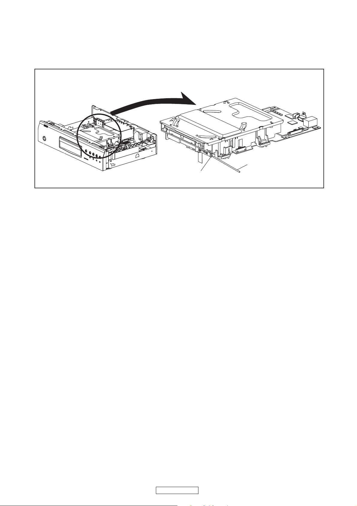
BD Mechanism Replacement Guidelines
The guidelines describe how to determine whether a BD Mechanism Assembly is defective or not.
Confirm that the malfunction is eliminated after replacing the defective BD Mechanism Assembly with a new one.
*The BD Mechanism Assembly shall be acceptable when the following test disc can be played successfully;
BD-ROM BLX-201S3(SONY) chp12
*Select [4: LD Test] and select [2: Operating Time] in Service Mode.
If the Operating Time shows 3,000 hours or more, the BD Mechanism Assembly shall be determined that it has
reached the end of its life.
Replacement of BD Main CBA & BD Mechanism Assembly
1. Remove the Top Cover, Tray Panel, Front Assembly, Front Bracket, Video CBA and AV PCB Holder.
2. Disconnect Connectors and replace the BD Main CBA & BD Mechanism Assembly.
Refer to CABINET DISASSEMBLY INSTRUCTIONS.
BD Main CBA
& BD Mechanism Assembly
32
DN-V500BD

BLOCK DIAGRAMS
System Control Block Diagram
RS232C-
CONNECTOR
3 RXD
2TXD
RS232C CBA
IC5500
CN5500
RS232C
INTERFACE
13
14
RS232C
I/F
11
12
IC5550
REMOTE
-IN
REMOTE
-OUT
JK5550
1
2
(PHOTO COUPLER)
4
3
BUFFER
Q5551, Q5552
EV+3.3V
VFD
19 20 21 22
FL3001
D3003
POWER
FRONT A CBA
SENSOR
REMOTE
RS3001
-LED
STANDBY/POWER
66FL-RESET
55FL-STB
44FL-SCL
12 12REMOTE
CN2002 CN3002
BUFFER
Q2002
274934
REMOTE
33FL-SDA
33
FL-SDA
FL-SCL
FL-STB
15 15KEY-2
18 18
1
60
50
KEY-2
FL-RESET
D3002
STANDBY
POWER
SW3001
CN3001
KEY-2
1
KEY-1
2
16 16KEY-1
EV+3.3V
X2000
RESET
IC2001
62
KEY-1
14
RESET
8MHz
8
OSC1
X'TAL
9
OSC2
1
2
KEY
CN3101
SWITCH
KEY
SWITCH
FRONT B CBA
AUDIO CBA
CN5501
REMOTE
RS232C-RXD
RS232C-TXD
11
55
44
CN4002
VIDEO CBA
BD MAIN CBA
SUB-TXD
(SUB MICRO CONTROLLER)
RS232C-TXD
IC2000
45
CN2005
RS232C-TXD
REMOTE
22
66
CN4001
SUB-RXD
RS232C-RXD
46
RS232C-RXD
11
MUTE2
TO VIDEO
21 MUTE1
22 MUTE2
15 15MUTE1
14 14MUTE2
MUTE1
BLOCK
DIAGRAM
CN4000
CN7101
15
16
10 10SUB-TXD
11 11SUB-RXD
14 14SUB-TXD
13 13SUB-RXD
JK7501
SYS-RESET
3
Q2620, Q2621
Q2618
99SYS-RESET
17 17CEC
15 15SYS-RESET
17 17CEC
CEC
SWITCHING
BUFFER
13
CEC-OUT
28 CEC-IN
30
BUFFER
Q2619
STANDBY/POWER-LED
MAIN MICRO
IC6001
CONTROLLER
IC6903 (EEPROM)
U34
RXD1
SCL0
V31
6
SCL
V32
TXD1
SDA0
W30
5
SDA
AUDIO-MUTE
TO AUDIO
IC6401
(ETHERNET INTERFACE)
AUDIO-MUTE
24
BLOCK
DIAGRAM
MII-RXD0
MII-RXCLK
J4
2823222120
JK6401
ETHERNET
JACK
MII-RXD2
MII-RXD1
J2J1J3
121110
123
TX(-)
TX(+)
32 FL-SW
FL-SW
AE32
XTRST
MII-RXD3
MII-TXD0
MII-TXCLK
K2
H4
G4
33
ETHERNET
INTERFACE
9
6
RX(-)
RX(+)
PWSW237PWSW463FAN-LOCK
PWSW1
4
44
FAN-CONT1
PWSW2
PWSW4
PWSW1
TO POWER
SUPPLY
BLOCK
DIAGRAM
Q6702
T34
XRST
MII-TXD3
MII-TXD2
MII-TXD1
F4
H5
G5
39
383635
FAN-CONT1
25
FAN-LOCK
Q6701
RESET
IC6701
2 1
P-ON+1.8V
33
DN-V500BD

Digital Signal Process 1 Block Diagram
VIDEO SIGNAL AUDIO SIGNAL
TO DIGITAL SIGNAL
PROCESS 2 BLOCK
DIAGRAM
(IC6001)
BD+
CSS
AACS
(MAIN MICRO CONTROLLER/DIGITAL SIGNAL PROCESS)
IC6001
A28
B28
ASENV
H34
G34
C33
STREAM
FE
DIGITAL
B34
CONTROL
SIGNAL
PROCESS
SD ATA 1
SCLK1
J34
J33
SD ATA 2
M31
SCLK2
M32
TRACKING-CONTROL
E23
COPY
FOCUS1-CONTROL
A24
PROTECT
CPRM
FOCUS2-CONTROL
D23
EXPA-CONTROL
B22
EXPB-CONTROL
D22
SLED1-CONTROL
C24
SLED2-CONTROL
D24
LOAD-CONTROL
C22
TRAY-OUT
D21
TRAY-IN
E21
INLIMIT
B3
SPINDLE-CONTROL
E24
SPINDLE-FG
B25
20 SE02
18 SE01
MPX
IC201 (FRONT-END PROCESSOR)
97-100
CN101
61 WBL
59
/LPP
WOB
MATRIX
102-105
107-110
A-D 21-24
E-H 26-29
RF
RF
GENERATOR
868588
RF(-) 18
RF(+) 17
666554
53
SCLK1
EQUALIZER
87
SD ATA 2 40
BDRF(-) 15
BDRF(+) 14
SD ATA 1
83 78 79
SCLK2 38
IC604 (OP AMP)
1 2
22
TRACKING
ACTUATOR
IC603 (MOTOR DRIVE)
212019
CN101
TD 3
DRIVE
TR 4
FOCUS 1
FD1 1
FR1 2
7 6
ACTUATOR
DRIVE
18
FD2 6
FOCUS 2
17
FR2 5
EXPA(+) 9
8 9
12
ACTUATOR
DRIVE
16
EXPA(-) 7
EXPB(-) 8
EXPB(+) 10
132310
COLLIMATE
IC602 (MOTOR DRIVE)
236
LENS
MOTOR DRIVE
5
4
SLED
IC603 (MOTOR DRIVE)
32
33
CN601
SLD2(-) 3
SLD2(+) 4
30
MOTOR DRIVE
2
1
SLD1(-) 1
SLD1(+) 2
LOADING
14
CN602
LOAD(+) 5
13
MOTOR DRIVE
15
LOAD(-) 6
TRAY-OUT 2
BD MAIN CBA
SPINDLE
U3
HU(+) 5
MOTOR
HU(-) 6
4
DRIVE
HV(+) 7
12
HV(-) 8
HB(-) 11
HW(-) 10
HW(+) 9
10
IC601 (MOTOR DRIVE)
242119131415161718
CN603
V2
W1
INLIMIT 4
TRAY-IN 1
INNER
SW
BD MECHANISM
OEIC
(CD/DVD)
OEIC
(BD)
LASER
DIODE
DRIVE
34
DN-V500BD
SLED
MOTOR
LOADING
MOTOR
TRAY-OUT
TRAY-IN
SPINDLE
MOTOR

Digital Signal Process 2 Block Diagram
TO
VIDEO
BLOCK
DIAGRAM
VIDEO
VIDEO SIGNAL AUDIO SIGNAL
BP1-4-Y(0-1)
BP1-4-CR(0-1)
BP1-Y(0-1)
BP1-CO(0-1)
ABT-CB(0-11)
94-102,
108-110
SIGNAL
IC7201 (SCALER)
1-7,13-16,
176
BP1-CO(0-11)
ABT-Y(0-11)
111-114,
117-124
PROCESS
/SCALER
17-28
BP1-Y(0-11)
DQ (0-15)
IC7202 (SDRAM)
MEMORY
CONTROLLER
A (0-11)
SDRAM
BP1-P-CLK
BP1-VSYNC
BP1-HSYNC
12
173
174
ABT-P-CLK
ABT-HSYNC
107
ABT-P-CLK
IC6703 (CLOCK GENE.)
ABT-VSYNC
90
89
ABT-VSYNC
ABT-HSYNC
27MHz
X6701
1
789
IC7206
OSC
16
CLOCK
+3.3V
RESET
170
RESETN
SCL
163
2
SCL
GENE.
TO
VIDEO
BLOCK
DIAGRAM
MC
HDMI-LRCK
HDMI-SPDIF
MD
DAC-SCK
SCL3
SDA3
HDMI-BCK
HDMI-MCK
HDMI-DATA0
HDMI-DATA1
HDMI-DATA2
HDMI-DATA3
REC656-CLK
ANA-SW-CONT
SDA
164
3
SDA
10
DAC-BCK
DAC-LRCK
SPDIF
TO
AUDIO
BLOCK
DIAGRAM
MS2
MS3
MS4
MS5
DATA
MS1
DATA 3
DATA0
DATA1
DATA2
IC6001 (MAIN MICRO CONTROLLER/DIGITAL SIGNAL PROCESS)
C15
VIDEO
DAC
A5,E7
B8,E9
CN7601
55SDDAT0
DIGITAL
SD I/F
AF32,AG34,
SD DATA(0-3)
33SDDAT1
VIDEO
OUT
SDCLK
AH34
AH33,AJ34
77SDCLK
15 15SDDAT2
13 13SDDAT3
A4,A8,A9,B4,B9,C5,C9,
A3,A6,A7,B7,C4,C6,C7,
C8,D6,D9,E8,E12
C11,D8,D10,E10,E11
MEDIA
PROCESSOR
A2
B6
B5
E20
A19
AL5
D20
AL34
CLK
VSYNC
HSYNC
33M CLOCK
33M CLOCK
74M CLOCK
27M CLOCK
768K CLOCK
I/P CONVERTER
/SCALING
Java (BD-J)
MPEG-2
DiVX
VC-1
H.264
DECODER
TO
DIGITAL
SIGNAL
PROCESS 1
BLOCK
DIAGRAM
(IC6001)
ED (0-7)
R33
SCL3
HD (TS)
B18
U31
SDA3
ANA-SW-CONT
SD (PS)
D7
E13
B10
B11
REC656-CLK
A10
A11
D11
C12
C10
MEMORY
C0DQ (0-31)
C0A (0-12)
B14
A12
B13
A13
B12
E14
C14
D12
DIGITAL
AUDIO
OUT
I/F
D14
D13
C13
AC31
C1DQ (0-31)
C1A (0-12)
AC34
AD34
AC32
AC33
POWER
SD CBA
SUPPLY CBA
CN5003 CN5004
99SDDAT2
19 19SDDAT0
21 21SDDAT1
11 11SDDAT3
17 17SDCLK
CN5001
CN5000
SD
CARD
SLOT
BD MAIN CBA
DDR2 SDRAM
(NAND FLASH MEMORY)
IC6902
NAND FLASH
MEMORY (64M x 8bit)
(DDR2 SDRAM)
IC6501,IC6502
(1Gbit )
IC6601,IC6602
(DDR2 SDRAM)
DDR2 SDRAM
(512Mbit)
35
DN-V500BD

Video Block Diagram
VIDEO OUT
(COMPOSITE)
JK4004
JK4005
VIDEO-Y
OUT
VIDEO-Pb/Cb
OUT
JK4002
VIDEO-Pr/Cr
JK4003
OUT
TO SYSTEM
CONTROL
BLOCK
DIAGRAM
MUTE1
MUTE2
DDC DATA
DDC CLOCK
HOT PLUG
DETECT
191516
HDMI-CONNECTOR
JK7501
T.M.D.S DATA2-
T.M.D.S DATA2+
T.M.D.S DATA1-
T.M.D.S DATA1+
31649
T.M.D.S DATA0-
T.M.D.S DATA0+
7
T.M.D.S CLOCK+
T.M.D.S CLOCK-
10
12
VIDEO SIGNAL AUDIO SIGNAL
VIDEO CBABD MAIN CBA
C4018
WF3
75Ω
DRIVER
2dB
AMP
LPF 25
4dB
AMP
IC4000 (VIDEO DRIVER)
3
786
6.75MHz
75Ω
DRIVER
2dB
AMP
LPF
4dB
AMP
8 20
17
75Ω
2dB
LPF
13.5/37MHz
4dB
10
CN4000CN7101
33VIDEO
15
DRIVER
75Ω
DRIVER
AMP
2dB
AMP
LPF
13.5/37MHz
AMP
4dB
AMP
12
55VIDEO-Y(I/P)
77VIDEO-Pb/Cb
99VIDEO-Pr/Cr
Q7102
13.5/37MHz
WF1 WF2
2
13
MUTE1
MUTE2
118
DDC
AUTHENT
/CATION
KEY
EXCHANGE
REGISTER
IIC
I/F
113
116
CLK
121
IC7501 (HDMI INTERFACE)
23251921151713
120
119
TMDS
VIDEO
50,51,53-57,59,
87,88,90,91
SERIALIZER
TMDS
ENCODER
HDCP
CIPHER/
ENCRYPTOR
AV
CONTROLLER
I/F
70-73,75-78,
92,94,102,103
I/F
VS
HS
83
84
11
AUDIO
I/F
46454442413936
35
PLL
IC7205 (BUFFER)
1
IC7203
(VIDEO DAC)
IC7207
(SW)
VIDEO
2
136
ABT-P-CLK
3
63
30 CLKIN-A CLKIN-B
13
ANA-SW-CONT
REC656-CLK
555861
BP1-CO(0-1)
TO DIGITAL
SIGNAL
PROCESS 2
BLOCK
BUFFER
Q7103
BUFFER
434244
62
BP1-Y(0-1)
DIAGRAM
Q7101
BUFFER
VIDEO
DAC
535459
60
BP1-4-CR(0-1)
BP1-4-Y(0-1)
14-18,
25-29
ABT-CB(2-11)
2-9,
12,13
ABT-Y(2-11)
SCL
P-VSYNC
SDA
232221
20
S-VSYNC
P-HSYNC
S-HSYNC
49
50
SCL3
SDA3
ABT-HSYNC
ABT-VSYNC
ABT-CB(0-11)
ABT-Y(0-11)
TO DIGITAL
SIGNAL
PROCESS 2
BLOCK
DIAGRAM
HDMI-DATA0
HDMI-DATA1
HDMI-DATA2
HDMI-DATA3
HDMI-MCK
HDMI-BCK
HDMI-LRCK
HDMI-SPDIF
36
DN-V500BD

Audio Block Diagram
SURROUND(L)
-OUT
SURROUND(R)
-OUT
SUB
WOOFER
AUDIO SIGNAL
JK2202
(REAR)
AUDIO CBA
MUTE-ON
Q2631
DRIVE
Q2630
MUTE-ON
Q2632
-OUT
MUTE-ON
Q2627
DRIVE
Q2629
CENTER
-OUT
MUTE-ON
Q2628
DRIVE
Q2626
FRONT-
AUDIO(L)-
Q2624
Q2622
OUT
FRONT-
MUTE-ON
DRIVE
AUDIO(R)-
OUT
MUTE-ON
Q2625
DRIVE
Q2623
JK2203
(REAR)
SURROUND
BACK(L)-
Q2634
Q2633
OUT
MUTE-ON
DRIVE
SURROUND
BACK(R)-
Q2635
OUT
MUTE-ON
JK2200
(REAR)
AUDIO(L)-
OUT
JK2201
MUTE-ON
Q2203
DRIVE
Q2200
AUDIO(R)-
(REAR)
Q2202
Q2201
OUT
MUTE-ON
DRIVE
TO SYSTEM CONTROL
BLOCK DIAGRAM
AUDIO-MUTE
JK4000
(REAR)
Q4006
DIGITAL
AUDIO OUT
(COAXIAL)
BUFFER
IC2603
(OP AMP)
7
1
6
2
CN2007
SURROUND-MUTE
55SURROUND(L)
77SURROUND(R)
88
10 10SUB WOOFER
12 12CENTER
CN7001
14
15
7
IC2602
(OP AMP)
6
SUB WOOFER-MUTE
F-AUDIO(L)-MUTE
CENTER-MUTE
99
13 13
15 15FRONT-AUDIO(L)
17 17FRONT-AUDIO(R)
14 14
16
1
2
SURROUND BACK(R)
SURROUND BACK-MUTE
SURROUND BACK(L)
F-AUDIO(R)-MUTE
11
44
33
18 18
1
14
15
IC2601
(OP AMP)
16
7
1
6
2
14
15
1
IC2604
(OP AMP)
16
7
1
7
1
6
2
IC2200
(OP AMP)
6
2
WF4
CN2007
22 22AUDIO(L)
24 24AUDIO(R)
19 19AUDIO(L)-MUTE
20 20AUDIO(R)-MUTE
CN7001
1
14
14
15
16
15
CN7101 CN4000
16
VIDEO CBA
WF5
11 11SPDIF
(L-CH)
IC7003
(AUDIO D/A CONVERTER)
3458276
MCMDDAC-SCK
(R-CH)
AUDIO
DAC
DAC-BCK
DAC-LRCK
MS3
MUTE
DATA1
(L-CH)
(R-CH)
IC7004
(AUDIO D/A CONVERTER)
3458276
MUTE
AUDIO
DAC
MS4
MUTE
DATA2
(L-CH)
(R-CH)
IC7002
(AUDIO D/A CONVERTER)
3458276
MUTE
MUTE
AUDIO
DAC
IC7005
(AUDIO D/A CONVERTER)
MS2
DATA0
TO DIGITAL
SIGNAL
PROCESS 2
BLOCK DIAGRAM
37
DN-V500BD
(L-CH)
(R-CH)
AUDIO
DAC
3458276
MS5
MUTE
DATA3
(L-CH)
(R-CH)
IC7001
(AUDIO D/A CONVERTER)
3458276
MUTE
AUDIO
DAC
MS1
MUTE
DATA
BD MAIN CBA
SPDIF

Power Supply Block Diagram
TO BD MAIN
CBA
(CN6001)
P-ON+1.2V
P-ON+1.8V
2 P-ON+5V(1)
5,6 P-ON+3.3V
9-11
Q1019
CN1006
FAN-VCC 1
23 P-ON+5V(2)
17-20
FAN
CONTROL
2FAN-LOCK
3,4 P-ON+10.5V
CN1003
NOTE:
The voltage for parts in hot circuit is measured using
hot GND as a common terminal.
Q1017
FAN
CONTROL
Q1010
TO SYSTEM
CONTROL
BLOCK
DIAGRAM
F1
FL
FL-SW
FAN-LOCK
F2
Q2603
AUDIO+3.3V
P-ON+14.5V
EV+3.3V
PWSW1
PWSW2
PWSW4
FAN-CONT1
AUDIO CBA
Q2604
REG.
+3.3V
Q2636, D2625
CN2008
PWSW1
EV+5V
PWSW2
PWSW4
11
10 10
11 11
SW+14.5V
Q1013
SW+10.5V
Q1006
Q1008
LIMIT
CURRENT
Q1012, Q1014
13 13
CN1004
Q2601
Q2602
F1-IN
+FL
F2-IN
FAN-CONT1
FAN-LOCK
44
66
55
15 15
16 16
FAN
"Ce symbole reprèsente un fusible à fusion rapide."
"This symbol means fast operating fuse."
CAUTION !
For continued protection against fire hazard,
replace only with the same type fuse.
ATTENTION : Pour une protection continue les risqes
d'Incele n'utiliser que des fusible de même type.
Risk of fire-replace fuse as marked.
F
A V
POWER SUPPLY CBA
T1002
D1007, D1008,
F
A V
HOT CIRCUIT. BE CAREFUL.
11
2
BRIDGE
RECTIFIER
D1011, D1012
LINE
FILTER
L1001
F1001
2A/250V
IC1009
12
IC1002
SWITCHING
REG.
+1.2V
CONTROL
Q1015
15
4
2
13
Q1002
5
SWITCHING
CONTROL
1
3
IC1008
VDD
SW+5V
Q1011
Q1005
REG.
+3.3V
REG.
+1.8V
IC1010
Q1016
10
6
Q1001
Q1009
9
16
7
SW+5V
Q1007
REG.
14
6
IC1004
ERROR
VOLTAGE DET
1
4
2
3
HOT
SHUNT
D1029
ERROR
VOLTAGE DET
COLD
CN1002
AC120V
AC120V
11
22
AC CORD
CAUTION !
Fixed voltage (or Auto voltage selectable) power supply circuit is used in this unit.
If Main Fuse (F1001) is blown , check to see that all components in the power supply
circuit are not defective before you connect the AC plug to the AC power supply.
Otherwise it may cause some components in the power supply circuit to fail.
AC1001
CN1001
INLET CBA
DN-V500BD
38

SCHEMATIC DIAGRAMS AND TEST POINTS
Standard Notes
WARNING
Many electrical and mechanical parts in this chassis
have special characteristics. These characteristics
often pass unnoticed and the protection afforded by
them cannot necessarily be obtained by using
replacement components rated for higher voltage,
wattage, etc. Replacement parts that have these
special safety characteristics are identified in this
manual and its supplements; electrical components
having such features are identified by the mark “#” in
the schematic diagram and the parts list. Before
replacing any of these components, read the parts list
in this manual carefully. The use of substitute
replacement parts that do not have the same safety
characteristics as specified in the parts list may create
shock, fire, or other hazards.
Notes:
1. Do not use the part number shown on these
drawings for ordering. The correct part number is
shown in the parts list, and may be slightly
different or amended since these drawings were
prepared.
2. All resistance values are indicated in ohms
(K = 10
3. Resistor wattages are 1/4W or 1/6W unless
otherwise specified.
4. All capacitance values are indicated in PF
(P = 10
5. All voltages are DC voltages unless otherwise
specified.
3
, M = 106).
-6
PF).
39
DN-V500BD

LIST OF CAUTION, NOTES, AND SYMBOLS USED IN THE SCHEMATIC DIAGRAMS ON
THE FOLLOWING PAGES:
1. CAUTION:
FOR CONTINUED PROTECTION AGAINST FIRE HAZARD, REPLACE ONLY WITH THE
F
A V
SAME TYPE FUSE.
ATTENTION: POUR UNE PROTECTION CONTINUE LES RISQES D'INCELE N'UTILISER
QUE DES FUSIBLE DE MÊME TYPE.
RISK OF FIRE-REPLACE FUSE AS MARKED.
This symbol means fast operating fuse.
Ce symbole represente un fusible a fusion rapide.
2. CAUTION:
Fixed Voltage (or Auto voltage selectable) power supply circuit is used in this unit.
If Main Fuse (F1001) is blown, first check to see that all components in the power supply circuit are not
defective before you connect the AC plug to the AC power supply. Otherwise it may cause some components
in the power supply circuit to fail.
3. Note:
1. Do not use the part number shown on the drawings for ordering. The correct part number is shown in the
parts list, and may be slightly different or amended since the drawings were prepared.
2. To maintain original function and reliability of repaired units, use only original replacement parts which are
listed with their part numbers in the parts list section of the service manual.
4. Voltage indications for PLAY and STOP mode on the schematics are as shown below:
2
1
(Unit: Volt)
The same voltage for
both PLAY & STOP modes
5.0
3
5.0
(2.5)
Indicates that the voltage
is not consistent here.
PLAY mode
STOP mode
5. How to read converged lines
1-D3
Distinction Area
Line Number
(1 to 3 digits)
Examples:
1. "1-D3" means that line number "1" goes to the line number
"1" of the area "D3".
2. "1-B1" means that line number "1" goes to the line number
"1" of the area "B1".
3
AREA D3
2
1
ABCD
AREA B1
1-D3
1-B1
6. Test Point Information
: Indicates a test point with a jumper wire across a hole in the PCB.
: Used to indicate a test point with a component lead on foil side.
: Used to indicate a test point with no test pin.
: Used to indicate a test point with a test pin.
40
DN-V500BD

Audio 1/3 Schematic Diagram
41
DN-V500BD

Audio 2/3 Schematic Diagram
42
DN-V500BD

Audio 3/3 Schematic Diagram
43
DN-V500BD

Video Schematic Diagram
44
DN-V500BD

Power Supply & Inlet Schematic Diagram
CAUTION !
Fixed voltage (or Auto voltage selectable) power supply circuit is used in this unit.
If Main Fuse (F1001) is blown , check to see that all components in the power supply
circuit are not defective before you connect the AC plug to the AC power supply.
Otherwise it may cause some components in the power supply circuit to fail.
F
A V
CAUTION !
For continued protection against fire hazard,
replace only with the same type fuse.
ATTENTION : Pour une protection continue les risqes
d'Incele n'utiliser que des fusible de même type.
Risk of fire-replace fuse as marked.
"This symbol means fast operating fuse."
"Ce symbole reprèsente un fusible à fusion rapide."
NOTE:
The voltage for parts in hot circuit is measured using
hot GND as a common terminal.
45
DN-V500BD

Front A & Front B Schematic Diagram
46
DN-V500BD

RS232C Schematic Diagram
47
DN-V500BD

SD Schematic Diagram
48
DN-V500BD

BD Main 1/13 Schematic Diagram
1 NOTE:
The order of pins shown in this diagram is different from that of actual IC6001.
IC6001 is divided into nine and shown as IC6001 (1/9) ~ IC6001 (9/9) in this BD Main Schematic Diagram Section.
49
DN-V500BD

BD Main 2/13 Schematic Diagram
1 NOTE:
The order of pins shown in this diagram is different from that of actual IC6001.
IC6001 is divided into nine and shown as IC6001 (1/9) ~ IC6001 (9/9) in this BD Main Schematic Diagram Section.
50
DN-V500BD

BD Main 3/13 Schematic Diagram
1 NOTE:
The order of pins shown in this diagram is different from that of actual IC6001.
IC6001 is divided into nine and shown as IC6001 (1/9) ~ IC6001 (9/9) in this BD Main Schematic Diagram Section.
51
DN-V500BD

BD Main 4/13 Schematic Diagram
1 NOTE:
The order of pins shown in this diagram is different from that of actual IC6001.
IC6001 is divided into nine and shown as IC6001 (1/9) ~ IC6001 (9/9) in this BD Main Schematic Diagram Section.
52
DN-V500BD

BD Main 5/13 Schematic Diagram
1 NOTE:
The order of pins shown in this diagram is different from that of actual IC6001.
IC6001 is divided into nine and shown as IC6001 (1/9) ~ IC6001 (9/9) in this BD Main Schematic Diagram Section.
53
DN-V500BD

BD Main 6/13 Schematic Diagram
1 NOTE:
The order of pins shown in this diagram is different from that of actual IC6001.
IC6001 is divided into nine and shown as IC6001 (1/9) ~ IC6001 (9/9) in this BD Main Schematic Diagram Section.
54
DN-V500BD

BD Main 7/13 Schematic Diagram
1 NOTE:
The order of pins shown in this diagram is different from that of actual IC6001.
IC6001 is divided into nine and shown as IC6001 (1/9) ~ IC6001 (9/9) in this BD Main Schematic Diagram Section.
55
DN-V500BD

BD Main 8/13 Schematic Diagram
56
DN-V500BD

BD Main 9/13 Schematic Diagram
1 NOTE:
The order of pins shown in this diagram is different from that of actual IC6001.
IC6001 is divided into nine and shown as IC6001 (1/9) ~ IC6001 (9/9) in this BD Main Schematic Diagram Section.
57
DN-V500BD

BD Main 10/13 Schematic Diagram
58
DN-V500BD

BD Main 11/13 Schematic Diagram
1 NOTE:
The order of pins shown in this diagram is different from that of actual IC6001.
IC6001 is divided into nine and shown as IC6001 (1/9) ~ IC6001 (9/9) in this BD Main Schematic Diagram Section.
59
DN-V500BD

BD Main 12/13 Schematic Diagram
60
DN-V500BD

BD Main 13/13 Schematic Diagram
61
DN-V500BD

--MEMO--
62
DN-V500BD

WF1
20μs0.5VVIDEO-CVBS
VIDEO-Cr 0.2V 10
μ
s
VIDEO-Cb 0.2V 10
μ
s
AUDIO(L) 1V 0.5ms
SPDIF 1V 0.1
μ
s
Pin 9 of CN4000
WF2
Pin 7 of CN4000
WAVEFORMS
WF4
WF5
Pin 22 of CN2007
Pin 11 of CN4000
WF3
C4018 PLUS LEAD
NOTE:
Input Signal (DVD)
VIDEO: 75% COLOR BAR
AUDIO: 1KHz, 0dB
63
DN-V500BD

WIRING DIAGRAM
REMOTE
-OUT
RS232C-CONNECTOR
RS232C CBA
FRONT A CBA
CN3001CN3101
1
2
3
KEY-2
GND
KEY-1
123
FRONT B
CBA
FAN
AC CORD
SD CBA
SD CARD SLOT
REMOTE
-OUT
REMOTE
1
EV+5V
2
RS232C-PW-CONT
3
RS232C-TXD
4
CN5501
RS232C-RXD
5
GND
6
F1
1
FL
2
FL-SDA
3
FL-SCL
4
FL-STB
5
FL-RESET
6
GND
7
GND
8
F2
9
GND
10
CN3002
EV+3.3V
11
REMOTE
12
GND
13
EV+5V
14
KEY-2
15
KEY-1
16
NU
17
STANDBY/POWER-LED
18
AC120V
1
AC120V
2
CN1001
INLET CBA
WP
23
CD
22
SDDAT1
21
GND
20
SDDAT0
19
GND
18
SDCLK
17
D+3.3V
16
D+3.3V
15
GND
14
CMD
13
GND
12
SDDAT3
11
CN5001
GND
10
SDDAT2
9
GND
8
GND
7
GND
6
GND
5
GND
4
GND
3
GND
2
GND
1
FAN-VCC
FAN-LOCK
W007
10
11
12
13
14
15
16
17
18
23
22
21
20
19
18
17
16
15
14
13
12
11
10
1
2
3
4
5
6
1
2
3
4
5
6
7
8
9
1
2
1
2
9
8
7
6
5
4
3
2
1
CN4002
1
RS232C-RXD
1
CN2005 CN4001
CN2002
1
W009
EV+5V
1
CN1004 CN2008
CN1006
CN1002
CN5003
DIGITAL
AUDIO OUT
(COAXIAL)
VIDEO
-Pr/Cr
OUT
VIDEO
-Pb/Cb
OUT
VIDEO-Y
OUT
VIDEO
-OUT
4
3
2
GND
RS232C-TXD
RS232C-PW-CONT
4
2
3
AUDIO(R)
-OUT
AUDIO(L)
-OUT
FRONT-
AUDIO(R)
-OUT
FRONT-
AUDIO(L)
-OUT
SUB
WOOFER
-OUT
4
3
2
F1-IN
NU
P-ON+14.5V
4
3
2
7
6
5
8
REMOTE
EV+5V
GND
RDY
6
5
7
8
CENTER
-OUT
SURROUND
(R)-OUT
SURROUND
(L)-OUT
SURROUND
BACK
(R)-OUT
SURROUND
BACK
(L)-OUT
7
6
5
8
+FL
F2-IN
GND
GND
6
5
7
8
POWER SUPPLY CBA
VIDEO CBA
9
11
10
12
GND
SUB-RXD
SUB-TXD
SYS-RESET
9
12
11
10
9
11
10
12
FAN-CONT2(NU)
PWSW2
NU
PWSW1
9
12
11
10
14
15
16
13
MUTE1
VIDEO+5V
MUTE2
NU
15
16
14
13
AUDIO CBA
14
15
16
13
FAN-CONT1
FAN-LOCK
SAFETY
PWSW4
15
16
14
13
NU
1
GND
2
VIDEO
3
GND
4
VIDEO-Y(I/P)
5
GND
6
VIDEO-Pb/Cb
7
GND
8
VIDEO-Pr/Cr
9
GND
10
CN4000
SPDIF
11
GND
12
SUB-RXD
13
SUB-TXD
14
SYS-RESET
15
RDY
16
CEC
17
17
CEC
17
SURROUND BACK(R)
1
GND
2
SURROUND BACK(L)
3
SURROUND BACK-MUTE
4
SURROUND(L)
5
GND
6
SURROUND(R)
7
SURROUND-MUTE
8
SUB WOOFER-MUTE
9
SUB WOOFER
10
GND
11
CENTER
12
CENTER-MUTE
13
F-AUDIO(L)-MUTE
14
CN2007
FRONT-AUDIO(L)
15
GND
16
FRONT-AUDIO(R)
17
F-AUDIO(R)-MUTE
18
AUDIO(L)-MUTE
19
AUDIO(R)-MUTE
20
GND
21
AUDIO(L)
22
GND
23
AUDIO(R)
24
AUDIO+5V
25
AUDIO+5V
26
WP
1
CD
2
SDDAT1
3
GND
4
SDDAT0
5
GND
6
SDCLK
7
D+3.3V
8
D+3.3V
9
CN5004
GND
10
CMD
11
GND
12
SDDAT3
13
GND
14
SDDAT2
15
P-ON+5V(2)
23
GND
22
GND
21
P-ON+1.2V
20
P-ON+1.2V
19
P-ON+1.2V
18
P-ON+1.2V
17
GND
16
GND
15
GND
14
GND
13
GND
12
CN1003
P-ON+1.8V
11
P-ON+1.8V
10
P-ON+1.8V
9
GND
8
GND
7
P-ON+3.3V
6
P-ON+3.3V
5
P-ON+10.5V
4
P-ON+10.5V
3
P-ON+5V(1)
2
NU
1
W006
1
2
3
4
5
6
7
8
9
10
CN7101
11
12
13
14
15
16
17
1
2
3
4
5
6
7
8
9
10
11
12
13
14
CN7001
15
16
17
18
19
20
21
22
23
24
25
26
BD MAIN CBA
15
14
13
12
11
10
9
8
7
CN7601
6
5
4
3
2
1
23
22
21
20
19
18
17
16
15
14
13
12
CN6001
11
10
9
8
7
6
5
4
3
2
1
CN101CN601
CN603
CN602
EXPA(+)
EXPB(+)
PI-CONT
BDRF(+)
BDRF(-)
THERMO
SEN-LDD
SLD1(+)
SLD2(+)
FD1
FR1
FR2
FD2
EXPA(-)
EXPB(-)
SA-INT
GND
GND
RF(+)
RF(-)
GND
+5V
VC-PD
GND
GND
+3.3V
GND
GND
+5V
+8V
SCLK2
SD ATA 2
XREST
LDEN
TEST-V
SLD1(-)
SLD2(-)
+5V
HU(+)
HU(-)
HV(+)
HV(-)
HW(+)
HW(-)
HB(-)
TRAY-OUT
1
2
TD
3
TR
4
5
6
7
8
9
10
11
12
13
14
15
16
17
18
19
20
21
A
22
B
23
C
24
D
25
26
E
27
F
G
28
H
29
30
31
32
33
34
35
36
37
38
39
40
41
42
NU
43
44
NU
45
1
2
3
4
W
1
V
2
U
3
4
5
6
7
8
9
10
11
TRAY-IN
GND
INLIMIT
LOAD(+)
LOAD(-)
HDMI-CONNECTORETHERNET JACK
CD/DVD
-OEIC
LASER DIODE DRIVE
M
M
11
22
33
44
55
RELAY CBA
66
LENS DRIVE
BD-OEIC
BD-LD
CD-LD
PD-LD
DVD-LD
SLED
MOTOR
SPINDLE
MOTOR
BD MAIN CBA & BD MECHANISM ASSEMBLY
PICKUP
-OUT
TRAY
-IN
TRAY
SW
INNER
M
LOADING
MOTOR
64
DN-V500BD

LEAD IDENTIFICATIONS
2SA1980M Y
2SA1980MG-AT
2SC5343MG-AT
KRA104M-AT/P
KRC102M-AT/P
KRC103M-AT/P
KRC106M-AT/P
KTC3199-GR-AT/P
KTA1267(GR, Y)-AT/P
RN1203(TE4 F T)
RN1206
SRA2204M-AT
ECB
SRC1202M-AT
SRC1206M-AT
SRC1203MAT
BD9323EFJ-E2
FA5573N-D1-TE1
8 5
1 4
EL817(B, C)
LTV-817(B, C)-F
PS2561A-1(W)
1
2
1: Anode
4
2: Cathode
3
3: Emitter
4: Collector
2SA1015-(GR, Y)(TE2 F T)
2SA1981Y-AT
2SA950-Y(TE2 F T)
2SA966-Y(TE6 F M)
2SC1815-GR(TE2 F T)
2SC2120-Y(TE2 F T)
2SC5344 Y
KTA1271-Y-AT/P
KTC3203-Y-AT/P
STB1277LY-AT
ECB
PST8430NR
S-80930CNMC-G80T2(G, J)
54
123
KTA1273-Y-AT/P
RA K
KHB4D5N60F-U/PMC
NJM4580E-TE1
85
GDS
14
MN101C77A GC
48
49
64
1
PQ070XF01SZH
PQ070XFC1SZF
1234
MM1757EHBE
33
32
17
28
1
16
KTC2026-Y/P 2SK3563(Q)
2SK3563(Q M)
ECB
GDS
15
14
ADM232AARN
SP232ACN-L/TR
16
1
STC403
BCE
2SC3928A-T112-1Z
2SC5343SFG
2SC5343SG
KTC3875S-GR-RTK/P
9
BE
8
C
Note:
A: Anode
K: Cathode
E: Emitter
C: Collector
B: Base
R: Reference
G: Gate
D: Drain
S: Source
65
DN-V500BD

--MEMO--
66
DN-V500BD

EXPLODED VIEW
Audio CBA
2L032
W006
RS232C CBA
2L032
W009
Video CBA
2L028
B70
2L056
B71
2L034
2L054
2L082
A3
A26
A14
B72
BD Main CBA &
BD Mechanism
Assembly
A26
A26
FM1001
2L081
2L061
2L070
2L081
2L070
2L079
2L073
2L081
2L082
2L082
2L083
2L072
2L089
2L081
A8
2L064
Front A CBA
A1X
2L036
2L018
B2
2L018
2L064
2L018
Front B CBA
SD CBA
2L018
2L051
2L036
2L057
A2
A6
B73
2L040
A6
A22
A6
2L036
W007
2L015
A4
A21
Inlet CBA
2L027
Power Supply CBA
2L026
B4
67
DN-V500BD

--MEMO--
68
DN-V500BD

PARTS LIST OF EXPLODED VIEW
* Parts for which "nsp" is indicated on this table cannot be supplied.
P.W.B. ASS'Y for which "nsp" is indicated on this table cannot be supplied. When repairing the P.W.B. ASS'Y, check the board parts table and order replacement parts
*
* The parts listed below are for maintenance only, might differ from the parts used in the unit in appearances or dimensions.
Ref. No. Part No. Part Name Remarks Q'ty New
9H2189002080D AV ASSEMBLY
- VIDEO CBA
-AUDIO CBA
- FRONT A CBA
- FRONT B CBA
1VSA21865
-
-
-
-
1
.
9H2189002090D POWER ASSEMBLY
- POWER SUPPLY CBA
- RS232C CBA
-SD CBA
-INLET CBA
1B1 9H2309002070D BD MAIN CBA & BD MECHANISM ASSEMBLY
A1X 9H2402002820P FRONT ASSEMBLY E5KA4UD
A2 nsp CHASSIS E5KA0UD
A3 9H2403001970D TOP COVER E5KA0UD
A4 9H2406003000P REAR PANEL E5KA4UD
A6 9H2407001020S FOOT ASSEMBLY E5H50UD
A8 9H2418001990D TRAY PANEL ASSEMBLY E5KA0UD
A14 nsp TOP PLATE E5KA0UD
A21 nsp LABEL SERIAL NO. E57E0UD
A22 nsp LICENSE LABEL E5KA0UD
A26 nsp DOUBLE SIDE TAPE E5KA0UD
B2 nsp FRONT BRACKET E5KA0UD
B4 nsp POWER HOLDER E5KA0UD
B70 nsp HIMELON TAPE(5X40) E5KA0UD
B71 nsp HIMELON TAPE
B72 nsp AV PCB BRACKET E5KA0UD
B73 nsp LOADER BRACKET E5KA0UD
FM1001 9H2685001110S MOTOR DC FAN 2D65BL100190
W006 9H2606002000S WIRE ASSEMBLY FFC 26/169/1.0
W007 nsp WIRE ASSEMBLY VH 2/265/AWG20
W009 nsp WIRE ASSEMBLY PH 16/290/AWG24
1VSA21844
-
-
-
-
N77D0BUN
1VM123899
1VM021192
1VM021193
1VM228277
1VM430199
1VM227177
1VM226936
-
-
1VM329678
1VM122941
1VM122880
1VM431686
-
1VM226905
1VM122901
MMEZR12XNR08
WX1E5KA0-006
WX1E5KA0-007
WX1E5KA0-009
1
1
1*
1
1
1*
4
1
1
1
1
3
1
1
1
1
1
1
1
1
1
1
SCREWS
2L015 nsp SCREW TAP TIGHT WASHER+ P-TIGHT
2L018 nsp SCREW P-TIGHT M3X8 BIND HEAD+
2L026 nsp SCREW S-TIGHT M3X6 E5E10UD
2L027 nsp SCREW S-TIGHT M3X6 E5E10UD
2L028 nsp SCREW S-TIGHT M3X10 E5610UD
2L032 nsp SCREW S-TIGHT M3X6 E5E10UD
2L034 nsp SCREW S-TIGHT M3X6 E5E10UD
2L036 nsp SCREW S-TIGHT M3X6 BIND HEAD+
2L040 nsp SCREW TAP TIGHT WSHAER +P-TIGHT
2L051 nsp SCREW TAP TIGHT WASHER+ P-TIGHT
2L054 nsp SCREW C-TIGHT M3X6 E5610UD
2L056 nsp SCREW S-TIGHT M3X6 E5E10UD
2L057 nsp SCREW S-TIGHT M3X6 E5E10UD
2L061 nsp HEXAGON SPACER E6AE0UD
69
DN-V500BD
GCJP3080
GBJP3080
1VM429667
1VM429667
0VM412936A
1VM429667
1VM429667
GBJS3060
GCJP3080
GCJP3080
0VM412937A
1VM429667
1VM429667
1VM424730
3
9
3
2
4
5
4
7
4
2
6
4
1
2

Ref. No. Part No. Part Name Remarks Q'ty New
2L064 nsp SCREW S-TIGHT M3X8 DISH HEAD+
2L070 nsp B-TIGHT SCREW M3X8 E5E00UD
2L072 nsp B-TIGHT SCREW M3X8 E5E00UD
2L073 nsp B-TIGHT SCREW M3X8 E5E00UD
2L079 nsp S-TIGHT SCREW M3X6 E5E00UD
2L081 nsp S-TIGHT SCREW M3X6 E5E00UD
2L082 nsp SCREW TAP TIGHT M3X5 BIND HEAD+BLK NI
2L083 nsp S-TIGHT SCREW M3X6 E5E00UD
2L089 nsp S-TIGHT SCREW M3X6 E5E00UD
GDHS3080
1VM428563
1VM428563
1VM428563
1VM428564
1VM428564
GBHC3050
1VM428564
1VM428564
5
11
1
2
1
5
9
1
2
70
DN-V500BD

PACKING VIEW
Lower SideUpper Side
S1
S3
X1
X12
X3
X19
z
X15 X14 X6
X10
A30
S1
A20
A30
S2
71
DN-V500BD

PARTS LIST OF PACKING & ACCESSORIES
* Parts for which "nsp" is indicated on this table cannot be supplied.
* The parts listed below are for maintenance only, might differ from the parts used in the unit in appearances or dimensions.
Ref. No. Part No. Part Name Remarks Q'ty New
A20 nsp BAR CODE LABEL E5KA4UD
A30 nsp CONTROL LABEL E5KA4UD
S1 9H2533002010D SIDE PAD E5KA0UD
S2 9H2531002810P GIFT BOX CARTON E5KA4UD
S3 nsp SET BAG E7708UA
X1 9H2541003010P OWNERS MANUAL E5KA4UD
X3 00D5150966206 WARRANTY(COM.1Y)
X6 nsp MANGANESE DRY BATTERY R6UWC/2STA
X6 nsp MANGANESE DRY BATTERY R6UWC/2SK
X6 nsp DRY BATTERY ES-GR6M-C
X10 nsp ACCESSORY BAG E5795ED
X12 nsp S.S.LIST COM.(EX)
X14 nsp AV CORD 1000/BLACK
X14 nsp AV CORD RCA(M*2)TO RCA(M*2)
z X15 00D9H26000887
z X15 nsp
X19 9H2307002060D REMOTE CONTROL UNIT NB420UD
X38 nsp WARRANTY SHEET E6E80UD
AC CORD WITH A GND WIRE UL/CSA/ 162/NO/BLACK
CORD W/O A GND WIRE UL/CSA(VW-1)/152/NO/
1VM123019
1VM331399
0DM400731D
1VMN28114
XB0M311MS003
XB0M311MS002
XB0M571GLP01
0VM416059
1VM323388
WPZ0102TM018
WPZ0102LTE01
WAV0162LW001
WAV0152LTE01
NB420UD
1VM323952A
-
-
-
1
2
2
1*
1
1*
1*
2
2
2
1
1
1
1
1
1
1
1
72
DN-V500BD
 Loading...