

Page 1
For U.S.A., Canada, Europe,
Korea & Japan model
SERVICE MANUAL
3
Ver. 3
Please refer to the
MODIFICATION NOTICE.
MODEL
STEREO CD/MP3 PLAYER
DN-C635
注 意
サービスをおこなう前に、このサービスマニュアルを
必ずお読みください。本機は、火災、感電、けがなど
に対する安全性を確保するために、さまざまな配慮を
おこなっており、また法的には「電気用品安全法」に
もとづき、所定の許可を得て製造されております。
従ってサービスをおこなう際は、これらの安全性が維
持されるよう、このサービスマニュアルに記載されて
いる注意事項を必ずお守りください。
●
For purposes of improvement, specifications and
design are subject to change without notice.
●
Please use this service manual with referring to the
operating instructions without fail.
●
Some illustrations using in this service manual are
slightly different from the actual set.
●
●
●
●
TOKYO, JAPAN
本機の仕様は性能改良のため、予告なく変更すること
があります。
補修用性能部品の保有期間は、製造打切後8年です。
修理の際は、必ず取扱説明書を参照の上、作業を行っ
てください。
本文中に使用しているイラストは、説明の都合上現物
と多少異なる場合があります。
X0169V.03 DE/CDM 0603
Page 2
SAFETY PRECAUTIONS
The following check should be performed for the continued protection of the customer and service technician.
LEAKAGE CURRENT CHECK
Before returning the unit to the customer, make sure you make either (1) a leakage current check or (2) a line to chassis
resistance check. If the leakage current exceeds 0.5 milliamps, or if the resistance from chassis to either side of the power
cord is less than 460 kohms, the unit is defective.
LASER RADIATION
Do not stare into beam or view directly with optical instruments, class 3A laser product.
DN-C635
2
CAUTION
Please heed the points listed below during servicing and inspection.
◎ Heed the cautions!
Spots requiring particular attention when servicing, such as
the cabinet, parts, chassis, etc., have cautions indicated on
labels or seals. Be sure to heed these cautions and the cautions indicated in the handling instructions.
◎ Caution concerning electric shock!
(1) An AC voltage is impressed on this set, so touching inter-
nal metal parts when the set is energized could cause
electric shock. Take care to avoid electric shock, by for example using an isolating transformer and gloves when
servicing while the set is energized, unplugging the power
cord when replacing parts, etc.
(2)There are high voltage parts inside. Handle with extra care
when the set is energized.
◎
Caution concerning disassembly and assembly!
Though great care is taken when manufacturing parts from
sheet metal, there may in some rare cases be burrs on the
edges of parts which could cause injury if fingers are moved
across them. Use gloves to protect your hands.
◎ Only use designated parts!
The set's parts have specific safety properties (fire resistance, voltage resistance, etc.). For replacement parts, be
sure to use parts which have the same properties. In particular, for the important safety parts that are marked ! on wiring
diagrams and parts lists, be sure to use the designated parts.
◎ Be sure to mount parts and arrange the
wires as they were originally!
For safety reasons, some parts use tape, tubes or other insulating materials, and some parts are mounted away from the
surface of printed circuit boards. Care is also taken with the
positions of the wires inside and clamps are used to keep
wires away from heating and high voltage parts, so be sure to
set everything back as it was originally.
◎ Inspect for safety after servicing!
Check that all screws, parts and wires removed or disconnected for servicing have been put back in their original positions, inspect that no parts around the area that has been
serviced have been negatively affected, conduct an insulation
check on the external metal connectors and between the
blades of the power plug, and otherwise check that safety is
ensured.
(Insulation check procedure)
Unplug the power cord from the power outlet, disconnect the
antenna, plugs, etc., and turn the power switch on. Using a
500V insulation resistance tester, check that the insulation resistance between the terminals of the power plug and the externally exposed metal parts (antenna terminal, headphones
terminal, microphone terminal, input terminal, etc.) is 1MΩ or
greater. If it is less, the set must be inspected and repaired.
CAUTION
Many of the electric and structural parts used in the set have
special safety properties. In most cases these properties are
difficult to distinguish by sight, and using replacement parts
with higher ratings (rated power and withstand voltage) does
not necessarily guarantee that safety performance will be preserved. Parts with safety properties are indicated as shown
below on the wiring diagrams and parts lists is this service
manual. Be sure to replace them with parts with the designated part number.
(1) Schematic diagrams ... Indicated by the ! mark.
(2) Parts lists ... Indicated by the ! mark.
Concerning important safety parts
Using parts other than the designated parts
could result in electric shock, fires or other
dangerous situations.
注 意
サービス、点検時にはつぎのことにご注意願います。
◎注意事項をお守りください!
サービスのとき特に注意を必要とする個所についてはキャ
ビネット、部品、シャーシなどにラベルや捺印で注意事項を
表示しています。これらの注意書きおよび取扱説明書などの
注意事項を必ずお守りください。
◎感電に注意!
(1) このセットは、交流電圧が印加されていますので通電時
に内部金属部に触れると感電することがあります。従っ
て通電サービス時には、絶縁トランスの使用や手袋の着
用、部品交換には、電源プラグを抜くなどして感電にご
注意ください。
(2) 内部には高電圧の部分がありますので、通電時の取扱に
は十分ご注意ください。
◎分解、組み立て作業時のご注意!
板金部品の端面の『バリ』は、部品製造時に充分管理をして
おりますが、板金端面は鋭利となっている箇所が有りますの
で、部品端面に触れたまま指を動かすとまれに怪我をする場
合がありますので十分注意して作業して下さい。手の保護の
ために手袋を着用してください。
◎指定部品の使用!
セットの部品は難燃性や耐電圧など安全上の特性を持った
ものとなっています。従って交換部品は、使用されていたも
のと同じ特性の部品を使用してください。特に配線図、部品
!印で指定されている安全上重要な部品は必ず指定の
表に
ものをご使用ください。
◎部品の取付けや配線の引きまわしは、
元どおりに!
安全上、テープやチューブなどの絶縁材料を使用したり、プ
リント基板から浮かして取付けた部品があります。また内部
配線は引きまわしやクランパーによって発熱部品や高圧部
品に接近しないように配慮されていますので、これらは必ず
元どおりにしてください。
◎サービス後は安全点検を!
サービスのために取り外したねじ、部品、配線などが元どお
りになっているか、またサービスした個所の周辺を劣化させ
てしまったところがないかなどを点検し、外部金属端子部
と、電源プラグの刃の間の絶縁チェックをおこなうなど、安
全性が確保されていることを確認してください。
(絶縁チェックの方法)
電源コンセントから電源プラグを抜き、アンテナやプラグな
どを外し、電源スイッチを入れます。500V 絶縁抵抗計を用
いて、電源プラグのそれぞれの端子と外部露出金属部[アン
テナ端子、ヘッドホン端子マイク端子、入力端子など]との
間で、絶縁抵抗値が1 MΩ 以上であること、この値以下の
ときはセットの点検修理が必要です。
注 意
本機に使用している多くの電気部品、および機構部品は安全
上、特別な特性を持っています。この特性はほとんどの場合、
外観では判別つきにくく、またもとの部品より高い定格(定
格電力、耐圧)を持ったものを使用しても安全性が維持され
るとは、限りません。安全上の特性を持った部品は、この
サービスマニュアルの配線図、部品表につぎのように表示し
ていますので必ず指定されている部品番号のものを使用願
います。
(1) 配線図…!マークで表示しています。
(2) 部品表…!マークで表示しています。
安全上重要な部品について
指定された部品と異なるものを使用した場合に
は、感電、火災などの危険を生じる恐れがあり
ます。
2
Page 3
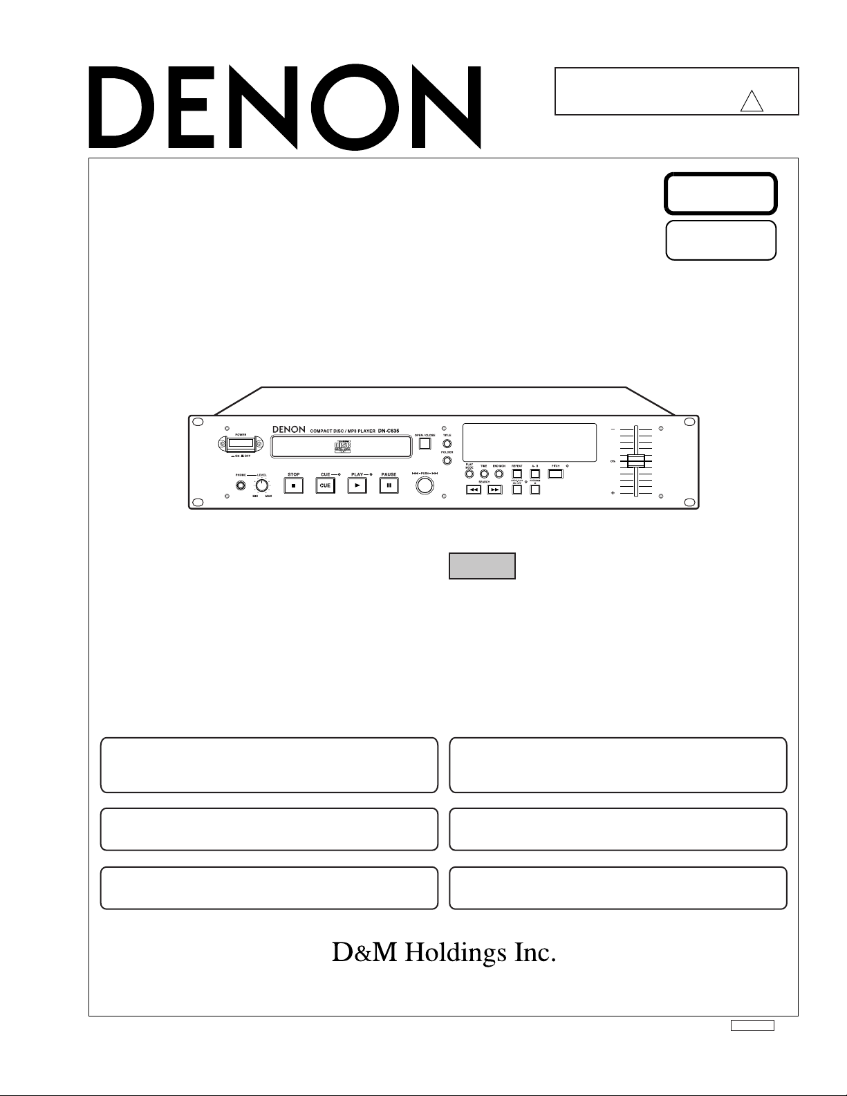
DN-C635
Top cover
3
DISASSEMBLY
(To reassemble, reverse disassembly)
1. TOP COVER
(1) Remove 4 screws on both sides, 1 screw on the rear side,
and 1 screw on the top side.
(2) Detach the Top Cover as shown in the arrow direction.
各部のはずしかた
(組み立てるときは、逆の順序で行ってください。)
1. TOPCOVER
(1) 両側面のねじ 4 本、後部のねじ 1 本と上面のねじ 1 本を
はずします。
(2) 上カバーを矢印の方向に取りはずします。
2. FRONT PANEL
(1) Remove 2 upper screws, 3 lower screws and 2 screws on
the both side.
(2) Detach the Front Panel in the arrow direction.
Front Panel
2. FRONTPANEL
(1) 上部のねじ 2 本、下部のねじ 3 本と両側面のねじ 2 本を
はずします。
(2) フロントパネルを矢印の方向に取りはずします。
3
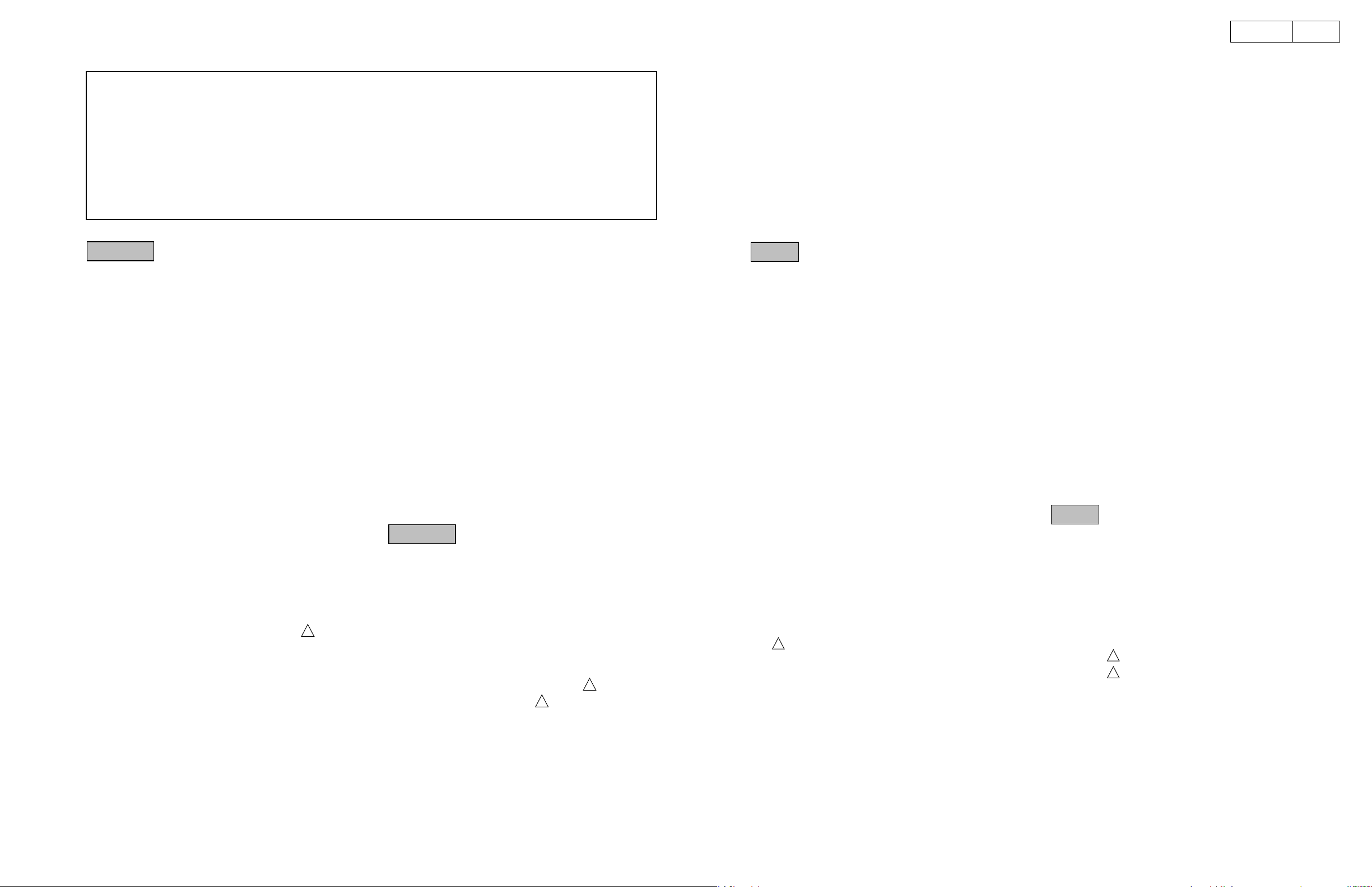
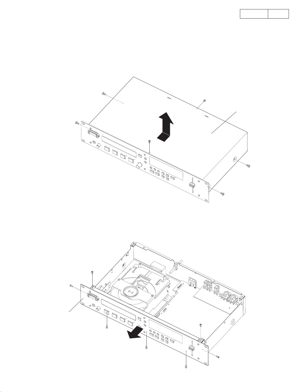
Page 4
DN-C635
Loader Panel
Mechanism Unit
4
3. MECHANISM UNIT
(1) Remove the Loder Panel.
(2) Remove 4 screws fixing the Mechanism Unit and detach
the Mechanism Unit.
3. MECHANISMUNIT
(1) ローダーパネルをはずします。
(2) メカ取付けねじ 4 本をはずし、メカユニットを矢印の方
向に取りはずします。
4
Page 5
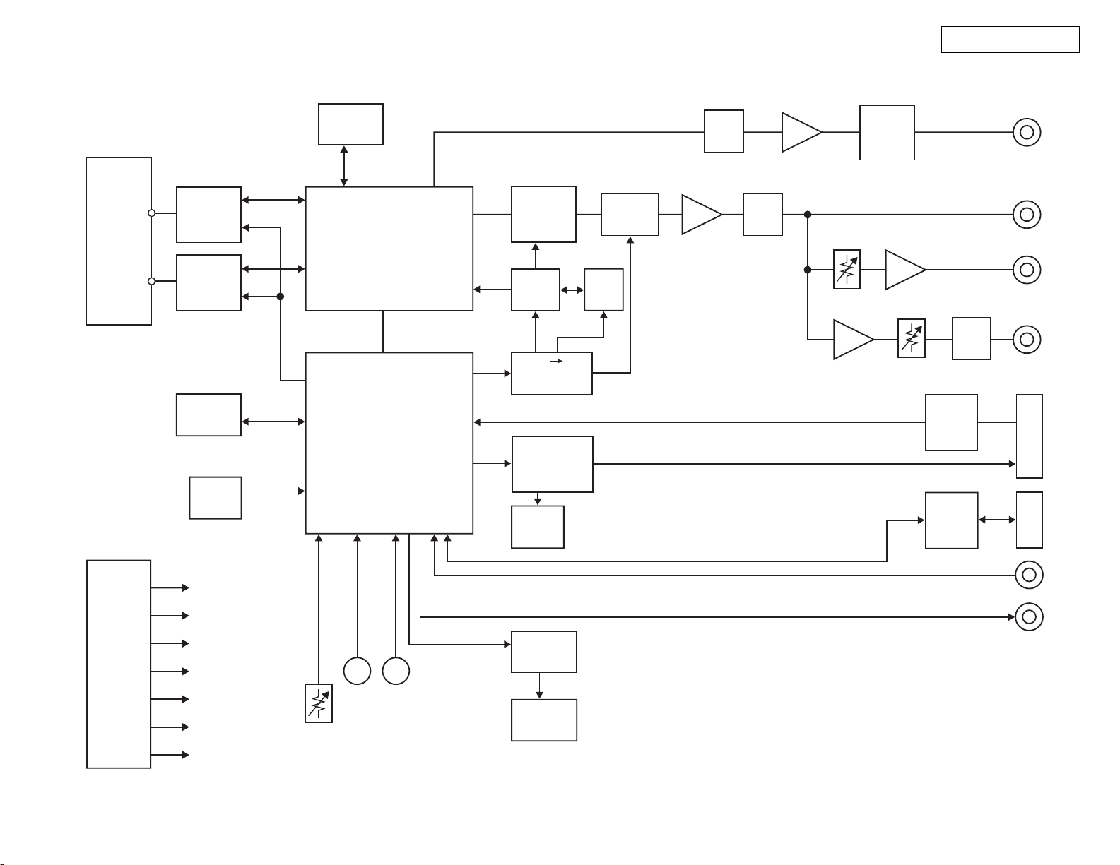
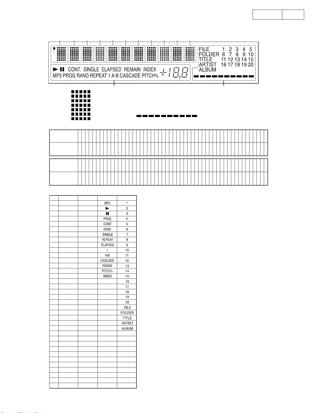
BLOCK DIAGRAM
5DN-C635
CD MECH.
MOTOR
ACTUATOR
P. U
DRIVER
AN8785SB
HEAD AMP
AN22002A
4M FLASH
ROM
KEY
16M DRAM
MN662791
SYSTEM µCOM
MN102H60KDA
DSP
DAC
PCM1716E
CLOCK
FIX/VARI
SELECT
3.3V 5V
I/F
TC74HCT7007
SERIAL/
PARALLEL
CONVERSION
LED
ST/MONO
SELECT
CLOCK
GEN.
±5V
MUTE
P. TRANS
DIGITAL
OUT
MUTE
CD OUT
±12V
XLR OUT
±5V
MUTE
H/P OUT
BUFFER
TALLY OUT
PARALLEL
RS232C
/422
POWER
SUPLY
±12V
±5V
+9V
+5V
+3.3V
-
HB
F1,F2
PITCH
ROTALY
ENCORDER
REMOTE
FLT
DRIVER
M66005FP
FLT
SERIAL
EXT IN
EXT OUT
5
Page 6
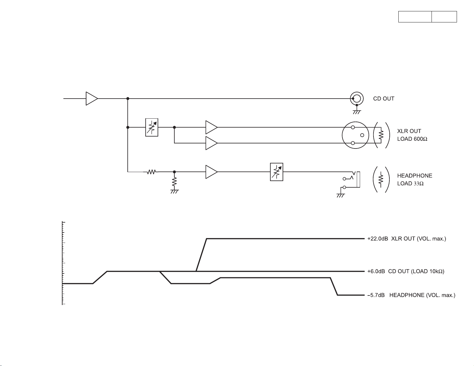
LEVEL DIAGRAM
6DN-C635
+30dB
+20dB
IC215
RCA
1 (7)
IC601 (602)
7
1
IC106
1 (7)
+10dB
0dB
-
10dB
0dB=1Vrms
0dB
+2.9dB
6
Page 7
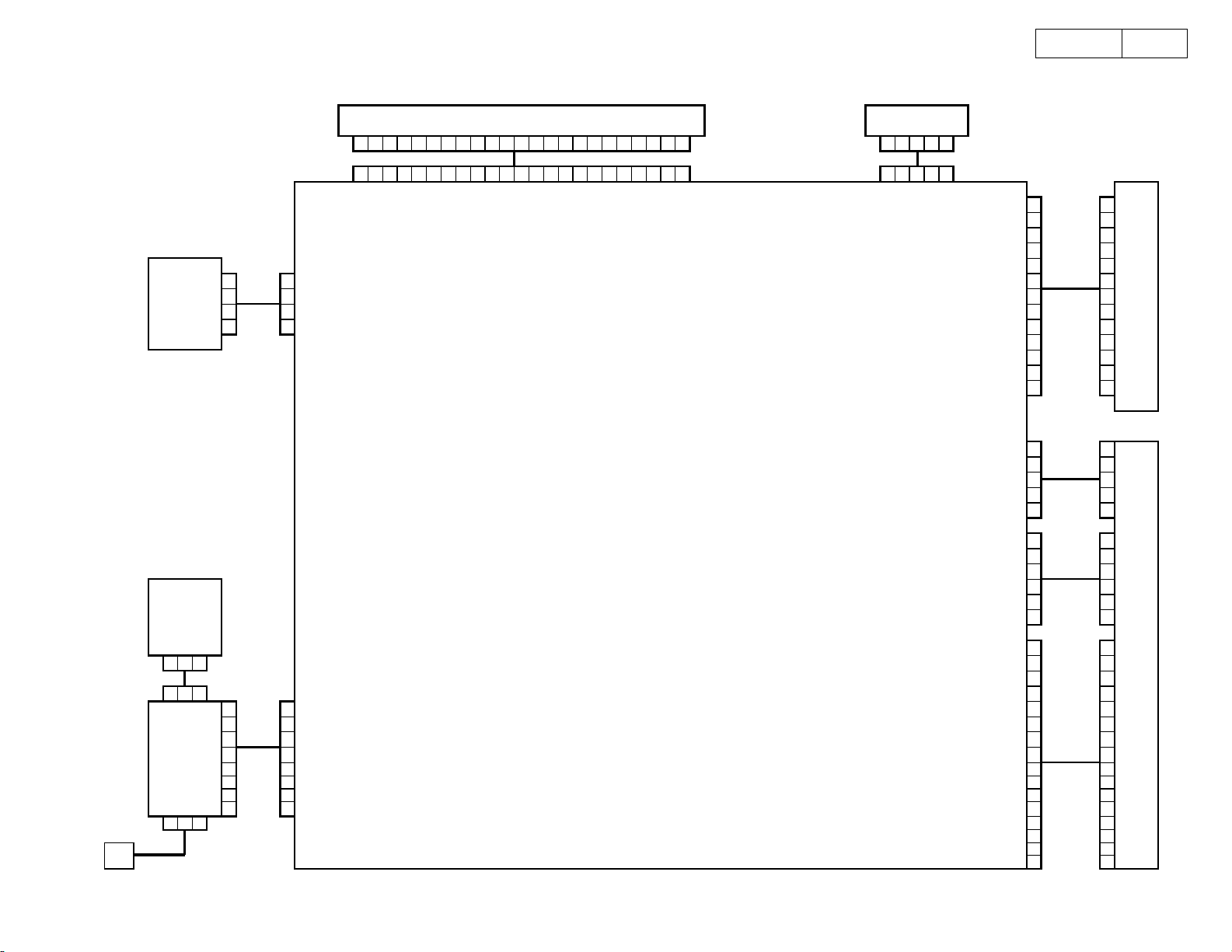
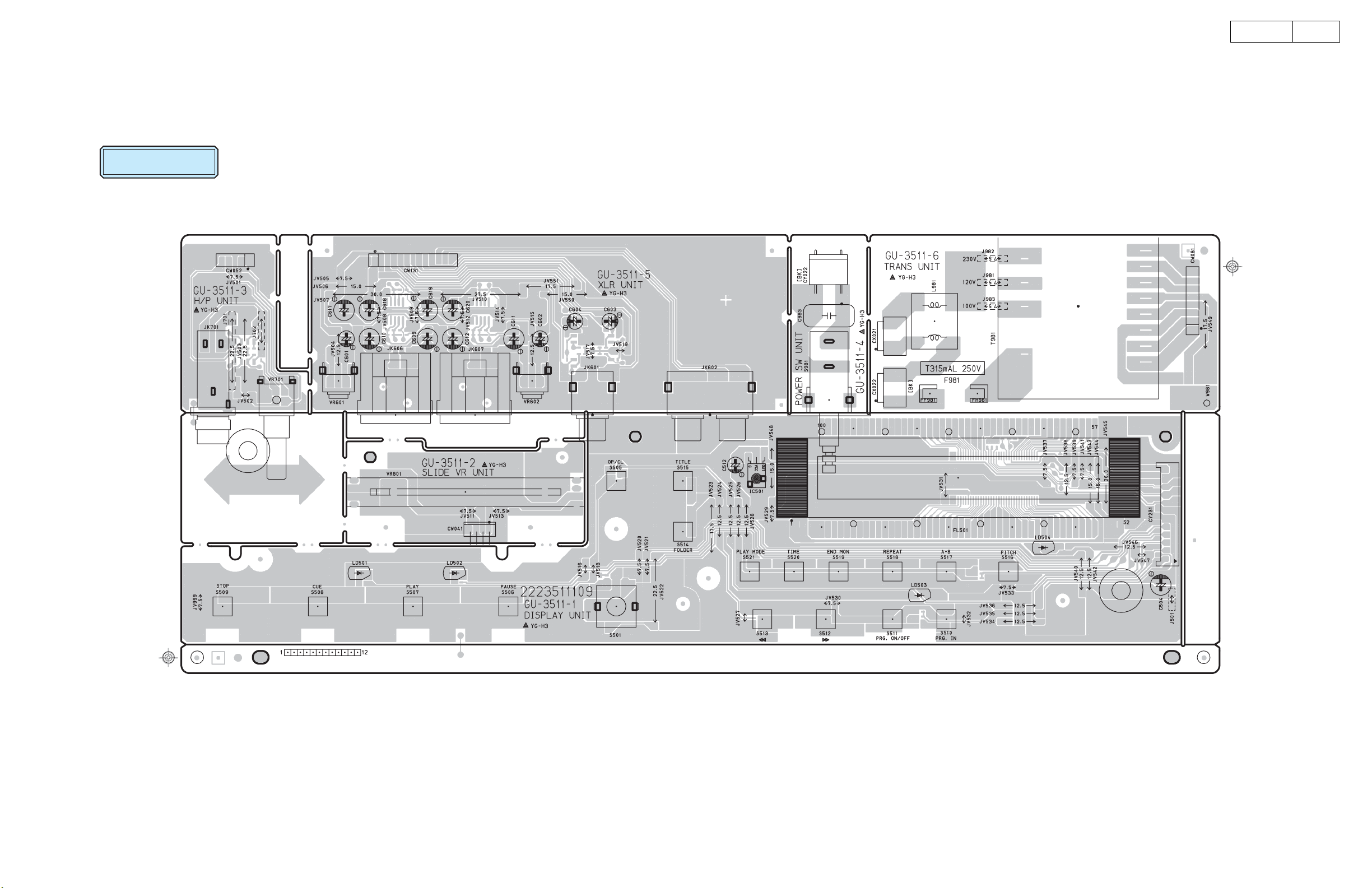
WIRING DIAGRAM
T
7DN-C635
AC
GU-3511-2
SLIDE VR.
UNIT
CW041
GU-3511-4
POWER SW
UNIT
CY022
12
12
CX022
GU-3511-6
TRANS UNI
CX021
12
GU-3511-1
PTHL
PRGL
CX231
CY231
KEYIN1
KEYIN2
KEYIN0
CY052
CX052
(RD) 1 1
23 22 21 20 19 18 17 16 15 14 13 12 11 10
123456789
F2
F1
-HB
GND
FLCK
FLRST-
11 66
22 77
33 88
44 99
PITCH
PITCHC
GND
+3.3V
10 11 12 13 14 15 16 17 18 19 20 21 22 23
FLDA
+3.3V
FLCS-
+3.3V
REMOTE
CX041
987654321 123
GND
GND
TRSLA-
PUSH-
TRSLB-
CUEL
PLYL
DISPLAY UNIT
GU-3511-3
H/P UNIT
45
45
123
GND
GND
H/P L
H/P R
MUTE
-12V
+12V
CDOUT R
GND
CDOUT L
MUTE
H/P R
GND
H/P L
GND
CAS IN
CAS OUT
EXT I/O
22
33
44
55
10 10
11 11
12 12
13 13
GU-3511-5 XLR UNIT
CX131
CW131
LOAD-
11
LOAD+
22
GU-3510
MAIN UNIT
(BK)
(BK)
11 55
22 66
33 77
44 88
55 99
66
77
88
CW081
CX081
CX051
CX062
CX161
OPEN
GND
CLOSE
LIMITSW-
LIMITSW+
SLED-
SLED+
SP-
SP+
VREF1
VCC
GND
NC
LPD
33
44
55
11
22
33
44
55
66
11
22
E
33
D
44
A
B
C
F
LD
10 10
11 11
12 12
F+
13 13
T-
14 14
T+
15 15
F-
16 16
CD MECH
7
Page 8
DN-C635
8
SERVICE PROGRAM
Required Measuring Implement
z Reference disc (TCD784 or CO-74176)
1. What is Service Program
Service program is a special program intended for confirming servo functions etc.
2. µcom Version Check
z Refer to "Preset Functions and Operations" of the instruction manual.
z You can check the µcom version.
3. Error Data Check
z Switch on the power while pushing the button and REPEAT button at the same time.
z After actuating the error data check program, press the CD's or button to display the logging error codes
in the occurred order.
XX Err** XX: occurred order
Err**: error code (Refer to the "Error Code Table" Page 9.)
z 10 error logs are memorized at maximum. Item 1 is newest data. Item 10 is oldest data. Item 2 is the 9th old data.
z Pressing the PAUSE button enters to data erase mode. ("Err Clear?" is displayed.)
If the PAUSE button is pressed again, the memorized error data are cleared.
To cancel the data erase mode, press the STOP button.
z To stop the Error Data check mode, please turn off the POWER switch.
NOTE: When the service is finished, delete the error logs.
4. Total Running Time
z Switch on the power while pushing the PROG. PLAY ON/OFF button and A-B button at the same time.
Total time span of CD that counted by the hour is displayed.
CD XXXXh
NOTE: Time is counted if the disc tray is opened first 30 minutes.
z Pressing the PAUSE button enters to data erase mode. ("Time Clear?" is displayed.)
If the PAUSE button is pressed again, the memorized time data are cleared.
To cancel the data erase mode, press the STOP button.
z To stop the Total Running Time check mode, please turn off the POWER switch.
NOTE: When the replacing the associated parts, delete the ranning time.
5. B.E.R. Checks and Automatic Servo Adjustment Call
z Switch on the power while pushing the button and END MON button at the same time.
And Loading a disc by OPEN/CLOSE button.
(1)Block Error Rate
Press the PLAY button. B.E.R. is displayed.
01Tr **m XXXX XXXX: Block Error Rate
You can select the track by the select knob.
(2)Tracking balance and Focus balance data
Press the TIME button. Tracking balance and Focus balance data is displayed.
2 ±XXX±@@@ XXX: Tracking balance
@@@: Focus balance
(3)Focus gain data
Press the END MON button. Focus gain data is displayed.
3 XXXX XXXX: Focus gain
(4)Tracking gain data
Press the REPEAT button. Tracking gain data is displayed.
4 XXXX XXXX: Tracking gain
(5)Tracking offset and Focus offset data
Press the A-B button. Tracking offset and Focus offset data is displayed.
5 ±XXX±@@@ XXX: Tracking offset
@@@: Focus offset
(6)Press the PLAY MODE button to select the Block Error Rate data.
(7)To stop the B.E.R. Check and Automatic Servo Adjustment Call mode,
please turn off the POWER switch.
No. botton Adjustment Item Adjustment Value indicator
-
2
3 Focus Gain 0576 ~ 2304
4 Tracking Gain 0392 ~ 1569
5
Tracking Balance
Focus Balance
Tracking Offset
Focus Offset
025 ~ +025
-
050 ~ +050
-
005 ~ +005
-
005 ~ +005
サービスプログラム
確認に必要な測定器具
●調整用ディスク:TCD784 又は CO-74176
1. サービスプログラムについて
サービスプログラムとは、サーボ機能等を確認するための特別なプログラムです。
2. マイコンバージョン確認
●取扱説明書の「プリセット機能と操作」を参照してください。
●マイコンバージョン確認ができます。
3. エラーデータ確認
● とREPEATボタンを同時に押しながら、電源スイッチを「ON」にします。
●エラーデータ確認プログラムが動作してから CD の または ボタンを押すと、エラーの発生した順にロギングされたエ
ラーコードが表示されます。
XXErr** XX:エラー発生順番(ログ番号)
Err**:エラーコード(9 ページの " エラーコード表 "を参照)
●最大10個のエラーが記録されます。(ログ番号1 が最も新しいデータで、ログ番号 10 が最も古いデータです。)
●PAUSE ボタンを押し続けると、エラーデータ消去モードになり、"ErrClear?" が表示されます。
この状態で再度 PAUSE ボタンを押すと、記録されたエラーデータが消去されます。
エラーデータ消去モードをキャンセルするには STOP ボタンを押します。
●エラーデータ確認モードを終わるには、電源スイッチを OFF にします。
注意:サービスプログラムを終了するときは、このエラーデータを消去して下さい。
4. トータルランニングタイム
●PROG.PLAYON/OFFと A-Bボタンを同時に押しながら、電源スイッチを「ON」にします。
CD のトータル再生時間が1時間単位で表示されます。
CDXXXXh
注意:ディスクトレイが最初の30分間でオープンになると(トータル再生)時間がカウントされます。
●PAUSE ボタンを押し続けると、トータルランニングタイム消去モードになり、"TimeClear?" が表示されます。
この状態で再度 PAUSE ボタンを押すと、記録されたトータルランニングタイムデータが消去されます。
トータルランニングタイム消去モードをキャンセルするには STOP ボタンを押します。
●トータルランニングタイム確認モードを終わるには、電源イッチを OFF にします。
注意:関連部品を交換したときは、このランニングタイムデータを消去して下さい。
5. B.E.R.確認と自動サーボ調整コール
● と ENDMONボタンを同時に押しながら、電源スイッチを「ON」にします。
OPEN/CLOSEボタンでディスクをローディングします。
(1) ブロックエラーレート
PLAYボタンを押すと、B.E.R. が表示されます。
01Tr**mXXXX XXXX:BlockErrorRate
SELECT ノブで測定するトラックを選択します。
(2) トラッキングバランスとフォーカスバランスデータ
TIMEボタンを押すと、トラッキングバランスとフォーカスバランスデータが表示されます。
2± XXX ± @@@ XXX:Trackingbalance
@@@:Focusbalance
(3) フォーカスゲインデータ
ENDMONボタンを押すと、フォーカスゲインデータが表示されます。
3XXXX XXXX:Focusgain
(4) トラッキングゲインデータ
REPEATボタンを押すと、トラッキングゲインデータが表示されます。
4XXXX XXXX:Trackinggain
(5) トラッキングオフセットとフォーカスオフセットデータ
A-Bボタンを押すと、トラッキンオフセットとフォーカスオフセットデータが表示されます。
5± XXX ± @@@ XXX:Trackingoffset
@@@:Focusoffset
(6)PLAYMODEボタンを押し、B.E.R.を表示させます。
(7) 電源スイッチを「OFF」にして、B.E.R.調整モードと自動サーボ調整コールモードを終了させます。
No.ボタン 調整項目 調整値
-
2
3 FocusGain 0576 〜 2304
4 TrackingGain 0392 〜 1569
5
TrackingBalance
FocusBalance
TrackingOffset
FocusOffset
025 〜 +025
-
050 〜 +050
-
005 〜 +005
-
005 〜 +005
8
Page 9
DN-C635
9
6. Test Mode (Heat Run mode)
z Switch on the power while pushing the FOLDER button and TIME button at the same time.
"000TroHR0000" is displayed. And the tray is opened.
(1)Hold the disc by the edges and place it on the disc tray.
(2)Starting with the OPEN/CLOSE button, it repeats open/close of the tray and playback.
***TrxHRXXXX ***: Track No.
x : o, c, s, t, r, and p
XXXX: Cycle quantity
All tracks are played back if the track count is less than 20.
Only the first and last tracks are played back if the tracks are more than 21.
When any errors, it stops and indicates error code (Refer to the Error Code Table).
(3)To stop the Test mode, please turn off the POWER switch.
7. Error Code Table
Error Code CONTENTS
Error 01 Unable to close the loader tray in the regulation time.
Error 02 Unable to open the loader tray in the regulation time.
Error 03 Inner circle switch ON error even if the time is over.
Error 04 Inner circle switch OFF error even if the time is over.
Error 05 The focus offset adjustment result is outside the regulation range.
Error 06 Unable to adjust the focus offset in the regulation time.
Error 07 The tracking offset adjustment result is outside the regulation range.
Error 08 Unable to adjust the tracking offset in the regulation time.
Error 09 The FE peak is outside the regulation range.
Error 0A The FE peak is outside the regulation range.
Error 0B Unable to adjust the focus rough gain in the regulation time.
Error 0C The focus rough gain is outside the regulation range.
Error 0D Unable to actuate focus in the regulation time.
Error 0E Unable to actuate tracking in the regulation time.
Error 0F Unable to adjust the tracking rough gain in the regulation time.
Error 10 The tracking rough gain is outside the regulation range.
Error 11 Unable to adjust the tracking balance in the regulation time.
Error 12 The tracking balance adjustment result is outside the regulation range.
Error 13 Focus servo down during automatic adjustment.
Error 14 Focus servo down during automatic adjustment.
Error 15 Unable to adjust the focus balance in the regulation time.
Error 16 The focus balance adjustment result is outside the regulation range.
Error 17 Track servo down during automatic adjustment.
Error 18 Unable to adjust the focus fine gain in the regulation time.
Error 19 The focus fine gain is outside the regulation range.
Error 1A Unable to adjust the tracking fine gain in the regulation time.
Error 1B The tracking fine gain is outside the regulation range.
Error 1C Unable to adjust automatically in the regulation time.
Error 1D Unable to read the subcode Q in the regulation time.
Error 1E Unable to read the TOC in the regulation time.
Error 1F Focus servo down during search (over the regulation time).
Error 20 Track servo down during search (over the regulation time).
Error 2116 Servo error during search.
Error 2103 Search error (over the regulation time).
Error 22 Discontinuity occurred, during write to the DRAM.
Error 23 The MP3 data could be read but not decoded.
Error 24 Unable to do the level detect.
6. テストモード(ヒートランモード)
●FOLDER と TIME ボタンを同時に押しながら、電源スイッチを「ON」にします。
"000TroHR0000"が表示され、トレイが開きます。
(1)ディスクをトレイに載せます。
(2)OPEN/CLOSE ボタンで(ヒートラン)を開始します。トレイの開閉と再生を繰り返します。
***TrxHRXXXX ***:TrackNo.
x:o,c,s,t,r,p
XXXX:ヒートランサイクル回数
20 トラック以下のディスクの場合、全トラックを再生します。
21 トラック以上のディスクの場合、最初のトラックと最終トラックのみを再生します。
(ヒートラン中に)エラーが発生すると、エラーコードを表示して停止します。(エラーコード表参照)
(3)テストモードを終了するには、電源スイッチを「OFF」にします。
7. エラーコード表
ErrorCode 内容
Error01 規定時間内にローダートレイがクローズできない
Error02 規定時間内にローダートレイがオープンできない
Error03 規定時間内に内周スイッチが ON されない
Error04 規定時間内に内周スイッチが OFF されない
Error05 フォーカスオフセット調整値が規定範囲外
Error06 規定時間内にフォーカスオフセット調整できない
Error07 トラッキングオフセット調整値が規定範囲外
Error08 規定時間内にトラッキングオフセット調整できない
Error09 FE ピークが規定の範囲外
Error0A FE ピークが規定の範囲外
Error0B 規定時間内にフォーカスラフゲインが調整できない
Error0C フォーカスラフゲインが規定範囲外
Error0D 規定時間内にフォーカスを駆動できない
Error0E 規定時間内にトラッキングを駆動できない
Error0F 規定時間内にトラッキングラフゲインを調整できない
Error10 トラッキングラフゲインが規定範囲外
Error11 規定時間内にトラッキングバランスが調整できない
Error12 トラッキングバランス調整値が規定範囲外
Error13 自動調整中にフォーカスサーボが落ちた
Error14 自動調整中にフォーカスサーボが落ちた
Error15 規定時間内にフォーカスバランスが調整できない
Error16 フォーカスバランス調整値が規定範囲外
Error17 自動調整中にトラックサーボが落ちた
Error18 規定時間内にフォーカスファインゲインが調整できない
Error19 フォーカスファインゲインが規定範囲外
Error1A 規定時間内にトラッキングファインゲインが調整できない
Error1B トラッキングファインゲインが規定範囲外
Error1C 規定時間内に自動調整ができない
Error1D 規定時間内にサブコード Q が読めない
Error1E 規定時間内に TOC が読めない
Error1F サーチ中にフォーカスサーボが規定時間以上落ちた
Error20 サーチ中にトラックサーボが規定時間以上落ちた
Error2116 サーチ中のサーボエラー
Error2103 (規定時間外での)サーチエラー
Error22 DRAM に書き込み中、不連続が発生
Error23 MP3 データはリードできたが、デコードすることができない
Error24 レベル検出できない
9
Page 10
DN-C635
10
Error Code CONTENTS
Error 25
Error 26 The error rate when recording on the memory is over the regulation value.
Error 27 The subcode jump more than regulation.
Error 28
Error 29 There was a subcode Q interruption, but the content of the subcode Q is abnormal.
Retried searching repeatedly, but the sound could not be connected, resulting in an
interruption of the sound.
The servo was turned on when the power was turned on, but did not start up in the regulation time.
µCOM VERSION UPGRADE
System µcom can be upgraded in the following manner.
Version Upgrade Method
1.Record the version upgrade software on a CD-R or CD-RW disc,
only as one file with the format ISO9660 Mode-1.
The file name of the supplied version upgrade software should be used as is and this disc needs
to finalize.
2.Hold the disc by the edges and place it on the disc tray.
3.Press the OPEN/CLOSE button to start the version upgrade.
"Versi on Up"→"Push Play!" "xxxx->XXXX" are displayed.
xxxx : current version
XXXX : upgrade version
4.Press the PLAY button.
"Now Writing" → "Writing-XXX" are displayed.
XXX : count up from 000 to129
5.When the version upgrade is finished, "Complete!" is indicated.
6.Turn off the power once and turn on again.
Press the OPEN/CLOSE button and remove the disc.
NOTE: When the power is turned off before "Complete!" is displayed,
µcom version is not written correctly.
ErrorCode 内容
Error25 サーチのリトライを繰り返したが、音をつなぐことができず音切れ発生
Error26 メモリに書き込み中にエラーレートが規定値を超えた
Error27 サブコードが規定以上飛んだ
Error28 電源投入時にサーボを起動したが、規定時間内にサーボがかからない
Error29 SUBQ の割り込みは入るが、Q データの内容が NG
マイコンアップグレード
本機は、次の方法でシステムマイコンのアップグレードを行うことができます。
アップグレードの方法
1.アップグレード用のソフトを、CD-R 又は CD-RW ディスクに ISO9660MODE1 のフォーマットでこのファイルだけを書き込みして
ください。
ファイル名は、配布された時のファイル名をそのまま使用し、ファイナライズしてください。
2.1 で作成したディスクをトレイに載せます。
3.OPEN/CLOSE ボタンを押すと、ディスクに書かれているアップグレードの情報を読み出します。
"VersionUp" → "PushPlay!""xxxx->XXXX"と表示されます。
xxxx:現在のバージョン
XXXX:新バージョン
4.PLAY ボタンを押すとアップグレードを開始します。
"NowWriting" → "Writing-XXX"と表示されます。
XXX:000から 129 までカウント Up します
5.アップグレードが終了すると"Complete!"が表示されます。
6.電源スイッチを切り、再び「ON」にします。
OPEN/CLOSE ボタンを押して、ディスクを取り出してください。
注意:"Complete!" が表示される前に電源スイッチを切ると、システムマイコンの新バージョンは正確に書き込みできません。
10
Page 11
DN-C635
DN-C635
BALANCED
OUT
Audio Transformer
1:1
600ohm
測定用LPF
(20kHz)
ひずみ率計/AFオシレータ
出力レベル調整用接続図
11
CONFIRMING THE AUDIO
1. Necessary Equipment for Adjustment
Distortion--Factor Meter
VTVM
Low-Pass Filter (20kHz)
AF Oscillator (20Hz ~ 20kHz, +18dBu)
Reference Disc; DENON Audio Technical CD (38C39-7174)
2. Output Level Adjustment
(1) Connect VTVM to the output connector of DN-C635.
Use 1:1 600 ohm Audio Transformer between the unit and VTVMs in order for matching the unbalanced input of
VTVM and the active balanced output of DN-C635 as shown in figure.
DN-C635
BALANCED
OUT
(2) Play track number "49".
(3) While reading VTVM indication, adjust VR602 (L-ch) and VR601 (R-ch) so that the output level attains +18dBu
(or desired level).
Audio Transformer
1:1
600ohm
LPF
(20kHz)
Connection for Output Level Adjustment
Distortion Meter
オーディオの確認方法
1. 必要な測定器具
ひずみ率計
VTVM
測定用フィルタ(20kHz)
AF オシレータ(20Hz 〜 20kHz,+18dBu)
調整用ディスク;DENONAudioTechnicalCD(38C39-7174)
2. 出力レベル調整
(1) VTVM を DN-C635 の BALANCEDOUT に接続します。
下図のとおり、DN-C635 のバランス出力と VTVM のバランス入力の間に入力インピーダンス 600Ω で 1:1 のレベル変換を行な
うオーディオトランスを接続して整合をとります。
(2) DN-C635 で調整用ディスクの 49 トラックを再生します。
(3) VTVM 表示は、出力レベルが +18dBu( 又は要求レベル ) になるように、レベル調整ボリューム VR602(L-ch)とVR601(R-ch)を
調整します。
R
VR601
Location of Level Adjustment VRs
L
VR602
R
VR601
L
VR602
レベル調整VRの位置
11
Page 12
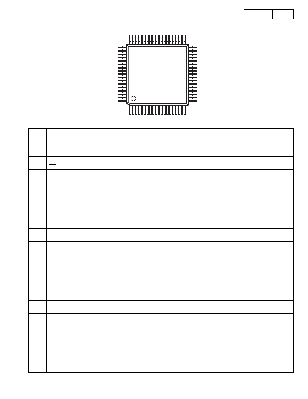
SEMICONDUCTORS
IC’s
MN102H60KDA
(IC103)
DN-C635
12
75
76
100
1
51
50
26
25
MN102H60KDA Terminal Function
Pin
No.
1 P60, WAIT, SBT2 PCDMUTE O - Pd L L Mute for CD
2 P61, _RE RD- O - Pu Hi-Z - Read signal
3 P62, _WEL WR- O - Pu Hi-Z - Write signal
4 P63, _WE, _WEH EXTIN- I - - Hi-Z - EXT.IN signal
5 _CS0,TM13OA FLASHROMCS- O - - Hi-Z - Chip select signal (MASK ROM operation : Input port)
6 _CS1, TM13OB PARALLELIN- O - - Hi-Z - Chip select signal (IN/OUT)
7 _CS2, TM14OA FLASHROMCS- I - - Hi-Z - Chip select signal (Normal operation : Input port, MASK ROM
8 _CS3, TM14OB -- O - - Hi-Z - Not used.
9 P54, _BREQ EXTOUT- O - - Hi-Z H EXT.OUT signal
10 P55, _BRACK RMTOUT- O - - Hi-Z H Remote output signal
11 P56, ALE, _ALE,
12 P57,_WORD WORD- I - H H H Data bit bus width select 'H': 8bit
13 P20,A00,SBT2 A00 A/O - - Unfix - Address bus
14 P21,A01,SBI2 A01 A/O - - Unfix - Address bus
15 P22,A02,SBO2 A02 A/O - - Unfix - Address bus
16 P23,A03 A03 A/O - - Unfix - Address bus
17 Vdd Vdd - - - - - Power supply (+3.3V)
18 BOSC,BIBT1,
19 Vss Vss - - - - - GND(0V)
20 XI,PB1 MCE O - Pd Hi-Z L Chip select 'L': MN662791 / 'H': BU2618
21 XO -- - - - - - Not used. OPEN
22 Vdd Vdd - - - - - Power supply (+3.3V)
23 OSCI OSCI I - - - -
24 OSCO OSCO O - - - - OSCI output
25 MODE MODE I - L L L Mode select 'L': Processor mode
26 P24,A04,TM15IA A04 A/O - - Unfix - Address bus
27 P25,A05 A05 A/O - - Unfix - Address bus
28 P26,A06 A06 A/O - - Unfix - Address bus
Pin Name Symbol I/O Det Ext Res Ini Function
operation : F. ROM Chip select)
MON2 I - - Hi-Z - Monitor signal 2
_BSTRE, TM15IA
IRINH O - - Hi-Z L Infrared remote 'L': Enable / 'H': Inhibit
BIBT2,PB0
12
Page 13
DN-C635
13
Pin
No.
29 P27,A07 A07 A/O - - Unfix - Address bus
30 P30,A08,_KI0 A08 A/O - - Unfix - Address bus
31 P31,A09,_KI1 A09 A/O - - Unfix - Address bus
32 P32,A10,_KI2 A10 A/O - - Unfix - Address bus
33 P33,A11,_KI3 A11 A/O - - Unfix - Address bus
34 AVDD AVDD - - - - - Analog power supply terminal
35 P34,A12,_KI4 A12 A/O - - Unfix - Address bus
36 P35,A13,_KI5 A13 A/O - - Unfix - Address bus
37 P36,A14,_KI6 A14 A/O - - Unfix - Address bus
38 P37,A15,_KI7 A15 A/O - - Unfix - Address bus
39 P40,A16 A16 A/O - - Unfix - Address bus
40 P41,A17 A17 A/O - - Unfix - Address bus
41 P42,A18 A18 A/O - - Unfix - Address bus
42 P43,A19 -- A/O - - Unfix - Address bus
43 Vref- Vref- - - - - - Standard analog power supply
44 P44,AN4,A20 KEYIN1 I Lv Pu Unfix - Panel key 1 (Use A/D converter)
45 P45,AN5,A21 KEYIN2 I Lv Pu Unfix - Panel key 2 (Use A/D converter)
46 P46,AN6,STOP,
47 P47,AN7,WDOUT,
48 P80,TM14OA TRSLA- I - Pu Hi-Z - Rotary switch A signal
49 P81,TM14OB TRSLB- I - Pu Hi-Z - Rotary switch B signal
50 P82,TM0IO,SBI2,
51 P83,TM4IO,SBI3 RxD I - - Hi-Z - Serial port (9600bps)
52 P84,TM7IO,SBO3,
53 P85,TM9IOA,
54 Vref+ Vref+ - - - - - Standard analog power supply
55 P86,TM9IOB,SBI4 FLCS- O - - Hi-Z H To FL driver CS
56 P87,TM9IC,SBO4,
57 P90,TM8IOA,
58 P91,TM10IOA,
59 P92,TM10IOB,
60 P93,TM10IC,
61 Vss Vss - - - - - GND (0V)
62 P94,AN0 -- I Lv Pd L - Not used.
63 P95,AN1 -- I Lv Pd L - Not used.
64 P96,AN2 PITCHC I Lv - Hi-Z - Use A/D converter
65 P97,AN3 PITCH I Lv - Hi-Z - Use A/D converter
66 Vdd Vdd - - - - - Power supply(+3.3V)
67 P70,SBT0,_RAS MCLK O - - Hi-Z H DSP interface Clock (clock synchronous formula)
68 P71,SBI0,_CAS,
69 P72,SBO0,_UCAS MDAT O - - Hi-Z H DSP interface Transmission (clock synchronous formula)
70 P73,SBT1,DUMX TXTCLK O - - Hi-Z H Use during CD-TEXT data read (clock synchronous formula)
71 P74,SBI1 PTXTD I - - Hi-Z - Use during CD-TEXT data read (clock synchronous formula)
Pin Name Symbol I/O Det Ext Res Ini Function
KEYIN3 I Lv Pu Unfix - Panel key 3 (Use A/D converter)
A22
SDA O - - Hi-Z L Serial data for BU2090
A23
MON1 I - - Hi-Z - Monitor signal 1
SBT3,SCL3
TxD O - - Hi-Z H Serial port (9600bps)
SDA3
FLCLK O - - Hi-Z H To FL driver SCK
SBO2,SBT4,SCL4
FLSD O - - Hi-Z H To FL driver SDATA
SDA4
LEDCK O - - Hi-Z L Clock for BU2090
BIBT1,_DMAREQ1
PUSH- I - Pu H - Not used.
BIBT2,_DMAACK1
LRCK I Ed - Hi-Z - LRCK : Use for time code creation during MP3 playback.
_DMAREQ0
NRST O - Pd L L Round IC reset signal
_DMAACK0
STAT I - - Hi-Z - DSP interface Reception (clock synchronous formula)
_LCAS
13
Page 14
DN-C635
14
Pin
No.
72 P75,SBO1 MLD O - - Hi-Z H DSP interface latch
73 TEST1 TEST1 I - Pu - - Pull up 33 - 50K
74 TEST2 TEST2 I - Pu - - Pull up 33 - 50K
75 _NMI -- I Lv Pu Hi-Z - Not used.
76 PA0,_IRQ0 BLKCK I Ed - Hi-Z - Sub code clock interruption
77 PA1,_IRQ1 DQSY I Ed - Hi-Z - CD-TEXT DQSY Interruption
78 PA2,_IRQ2 FADER ST I Ed - Hi-Z - Fader signal
79 PA3,_IRQ3 REMOTE- I Ed - Hi-Z - RC-5/Infrared remote signal input
80 PA4,_IRQ4,TM15IB CHGOFT O - Pu H L Off track signal
81 PA5,ADSEP ADSEP I - H H H H': Address data separation mode / 'L': Address data common mode
82 _RST RST- I Lv Pu L - Reset signal 'L': RESET
83 Vdd Vdd - - - - - Power supply (+3.3V)
84 P00,D00,AD00 D00 D/O - - Hi-Z - Data bus
85 P01,D01,AD01 D01 D/O - - Hi-Z - Data bus
86 P02,D02,AD02 D02 D/O - - Hi-Z - Data bus
87 P03,D03,AD03 D03 D/O - - Hi-Z - Data bus
88 P04,D04,AD04 D04 D/O - - Hi-Z - Data bus
89 P05,D05,AD05 D05 D/O - - Hi-Z - Data bus
90 P06,D06,AD06 D06 D/O - - Hi-Z - Data bus
91 P07,D07,AD07 D07 D/O - - Hi-Z - Data bus
92 Vss Vss - - - - - GND (0V)
93 P010,D08,AD08,
94 P011,D09,AD09,
95 P012,D10,AD10,
96 P013,D11,AD11,
97 P014,D12,AD12,
98 P015,D13,AD13,
99 P016,D14,AD14,
100 P017,D15,AD15,
Pin Name Symbol I/O Det Ext Res Ini Function
ST_MONO O - Pu H H Output mode STEREO/MONO=1/0
TM8IOB
FIX_VAR1 O - Pu H H VCO MORMAL/PITCH=0/1
TM8IC
TM11IOA
TM11IOB
TM11IC
TM12IOA
TM12IOB
TM12IC
DEBAG1 O - - - - Terminal 1 for debag
OPEN I - - Hi-Z - OPEN switch
CLOSE I - - Hi-Z - CLOSE switch
LOAD O - - Hi-Z H OPEN/CLOSE signal (PWM out put) (During Pnrst='L', out put
PWM(50%))
DEBAG1 O - - - H Terminal 2 for debag
LIMITSW- I O - Hi-Z - Inner circle SW
14
Page 15
MN6627911AC
(IC210)
61
60
41
40
DN-C635
15
80
1
20
MN6627911AC Terminal Function
Pin No. Pin Name I/O Function
1 DRVDD I Power supply for DRAM interface (Pin No.2 - 18, 80)
2 D0 I/O Data I/O signal 0 for DRAM
3 D1 I/O Data I/O signal 1 for DRAM
4 WE O Write enable signal for DRAM
5 RAS O RAS control signal for DRAM
6 D2 I/O Data I/O signal 2 for DRAM
7 D3 I/O Data I/O signal 3 for DRAM
8 CAS O CAS control signal 0 for DRAM
9 A10 O Address signal 10 for DRAM
10 A8 O Address signal 8 for DRAM
11 A7 O Address signal 7 for DRAM
12 A6 O Address signal 6 for DRAM
13 A5 O Address signal 5 for DRAM
14 A4 O Address signal 4 for DRAM
15 A9 O Address signal 9 for DRAM
16 A0 O Address signal 0 for DRAM
17 A1 O Address signal 1 for DRAM
18 A2 O Address signal 2 for DRAM
19 A3 O Address signal 3 for DRAM
20 DVSS2 I GND for digital
21 DVDD2 I Power supply for digital
22 SPOUT O Spindle motor drive signal
23 TRVP O Traverse drive signal
24 TRVM O Not used
25 TRP O Tracking drive
26 GCNTL O Gain control signal for CD-RW
27 FOP O Focus drive
28 CHGICO O EQ select signal
29 IOVDD1 I Power supply for IO
30 TBAL O Tracking balance adjust
31 FBAL O Focus balance adjust
32 FE I Focus error signal (Analog input)
33 TE I Tracking error signal (Analog input)
34 RFENV I RF envelope signal (Analog input)
35 OFT I Off track signal H : OFF TRACK
36 NRFDET I RF detect signal H : DETECT
21
15
Page 16
Pin No. Pin Name I/O Function
37 BDO I Drop out signal H : DROP OUT
38 LDON O Laser ON signal H : ON
39 ARF I RF signal
40 IREF I Standard current input terminal
41 ADPVCC I Voltage for power supply monitor
42 DSLF O Loop filter for DSL
43 RFSW I Loop filter for DSL
44 PLLF O Loop filter for PLL
45 PLLFO O Loop filter for PLL
46 AVDD2 I Power supply for analog (DSL, PLL, AD)
47 AVSS2 I GND for analog (DSL, PLL, AD)
48 OUTL O Not used
49 AVSS1 I GND for analog (Audio output)
50 OUTR O Not used
51 AVDD1 I Power supply for analog (Audio output)
52 DVSS3 I GND for digital
53 DVDD3 I Power supply for digital
54 TMOD2 I Test terminal L : Normal
55 MON2 O Serial monitor signal 2
56 BCLK O Bit clock for serial data
57 SRDATA O Serial data signal
58 LRCK O L, R discernment signal
59 IOVDD2 I Power supply for IO
60 TX O Digital audio interface signal
61 MCLK I ucon command clock signal
62 MDATA I ucon command data signal
63 MLD I ucon command load signal L : LOAD
64 BLKCK O Sub code block clock signal (f=75Hz : Normal speed playback)
65 PWMSEL I PWM output mode select L : Direct H : 3 values
66 SMCK O Not used
67 SBCK I Not used
68 STAT O Status signal
69 NRST I Reset L : RESET
70 SPPOL O Not used
71 PMCK O Not used
72 DQSY O Pack signal for CD TEXT data
73 TXTD O CD TEXT data signal
74 TXTCK O Ext. clock signal input for CD TEXT resister
75 NTEST I Test terminal H : Normal
76 X2 O Not used
77 X1 I 16.9344MHz input terminal
78 DVSS1 I GND for digital
79 DVDD1 I Power supply for digital
80 MON1 O Serial monitor signal
DN-C635
16
16
Page 17
AN8785SB
(IC202)
DN-C635
17
1
7
8
14 15
AN22002A
(IC201)
L: All mute
Hiz: ch2,4 ON
H: Active
28
22
21
Standby
16
Standby
Band-gap
Vcc/Vref
Reser Circuit
1.25V
+
-
7
IN2+
0.1µ
(2.5V)
PVcc2
10
[ Loading ]
D2+
D2-
M
12 11
-
-
+
-
+
9
ch.4 SW
H:2.5V
L or
IN2-
HIZ
+
8
:Vref
[ Traverse ]
D4-
18
-+-
21
IN4
-
D4+
+
17
+
switch
15
PGnd2
[ Others ]
[ Spindle ]
D3-
MM
14
-+-
-
20
IN3
CAGC
-
D1+
28
+
PGnd1
C0FTR
[ Tracking ]
D5-
D5+
26
+
-
+
2
IN5
0FTR
25
-
+
PVcc1
24
Protection
Circuit
22
SVcc
+
-
SGnd-Fin
4
IN-
5
IN+
3
OUT
6
Vref
[ Focus ]
D3+
PVcc3
D1-
13
+
19
1
-+-+-
+
23 27
IN1
CBD0
ARF
BD0
RFN
1
16
32
A
+
C
-
+
A
B
+
17
D
-
+
F
-
+
E
-
+
32
C
31
B
30
D
29
27
E
F
28
VREF
17
5
4
RFOUT
RF_EQ
AMP GCA BCA
AMP GCA BCA
AMP
AMP
+
-
6
NRFDET
GCA
GCA
8
7
RFIN
AGC BD0 0FTR
BCA
BCA
12
SUB
SUB
13
3TENV
-
+
-
+
14
9
CEA
10
3TOUT
15
NRFDET
FEN
22
23
FEOUT
TEN
21
20
TEOUT
TEBPF
11
19
VDET
-
+
LD
VDET
18
2
17
PD
1
TBAL
GCTL
24
26
FBAL
25
3
16
VCCGND
Page 18
PCM 1716E (IC211)
1
LRCIN
2
DIN
3
BCKIN
4
CLKO
5
XTI
6
XTO
7
DGND
8
V
DD
9
VCC2R
EXTR
NC
V
OUT
AGND1
10
11
12
13
R
14
AGND2R
28
27
26
25
24
23
22
21
20
19
18
17
16
15
ML/IIS
MC/DM1
MD/DM0
MUTE
MODE
CS/IWO
RST
ZERO
V
2L
CC
AGND2L
EXTL
NC
V
L
OUT
V
1
CC
DN-C635
PIN NAME I/O DESCRIPTION
1 LRCIN IN Left and Right Clock Input. This clock is equal to
the sampling rate - f
2 DIN IN Serial Audio Data Input
3 BCKIN IN Bit Clock Input for Serial Audio Data.
4 CLKO OUT Buffered Output of Oscillator. Equivalent to
System Clock.
5 XTI IN Oscillator Input (External Clock Input)
6 XTO OUT Oscillator Output
7 DGND
8V
9V
CC
10 AGND2R
-
Digital Ground
-
DD
2R
Digital Power +5V
-
Analog Power +5V
-
Analog Ground
11 EXTR OUT Rch, Common Pin of Analog Output Amp
-
12 NC
13 V
OUT
14 AGND1
15 V
CC
16 V
OUT
17 NC
R OUT Rch, Analog Voltage Output of Audio Signal
1
L OUT Lch, Analog Voltage Output of Audio Signal
No Connection
-
Analog Ground
-
Analog Power +5V
-
No Connection
18 EXTL OUT Lch, Common Pin of Analog Output Amp
-
19 AGND2L
20 V
2L
CC
Analog Ground
-
Analog Power +5V
21 ZERO OUT Zero Data Flag
22 RST IN Reset. When this pin is low, the DF and
modulators are held in reset.
23 CS/IWO IN Chip Select/Input Format Selection. When this
pin is low, the Mode Control is effective.
24 MODE IN
Mode Control Select. (H: Software, L: Hardware)
25 MUTE IN Mute Control
26 MD/DM0 IN Mode Control, DATA/De-emphasis Selection 1
27 MC/DM1 IN Mode Control, BCK/De-emphasis Selection 2
28 ML/I2S IN Mode Control, WDCK/Input Format Selection
NOTES: (1) Pins 1, 2, 3; Schmitt Trigger input. (2) Pins 22, 24, 25, 26, 27,
28; Schmitt Trigger input with pull-up resister. (3) Pin 23; Schmitt Trigger
input with pull-down resister.
(1)
.
S
(1)
(1)
(2)
(3)
18
(2)
(2)
(2)
(2)
BU2618FV (IC214)
18
Page 19
M66005FP (IC504)
D I G
1 1
1
2
D I G
1 0
3
D I G
0 9
D I G
0 8
4
D I G
0 7
5
D I G
0 6
6
D I G
0 5
7
D I G
0 4
8
9
D I G
0 3
D I G
0 2
1 0
D I G
0 1
1 1
D I G
0 0
1 2
1 3
R E S E T
C S
1 4
1 5
S C K
S D A T A
1 6
P I
1 7
P O
1 8
1 9
V c c 1
X
2 0
o u t
2 1
X
i n
2 2
V s s
S E G
2 3
3 5
2 4
S E G
3 4
S E G
3 3
2 5
S E G
3 2
2 6
S E G
3 1
2 7
2 8
S E G
3 0
S E G
2 9
2 9
S E G
2 8
3 0
S E G
2 7
3 1
V p S E G
3 2
D I G
6 4
6 3
D I G
6 2
D I G
D I G
6 1
6 0
V c c 2
5 9
S E G
S E G
5 8
S E G
5 7
5 6
S E G
5 5
S E G
5 4
S E G
5 3
S E G
5 2
S E G
5 1
S E G
5 0
S E G
4 9
S E G
4 8
S E G
4 7
S E G
4 6
S E G
S E G
4 5
S E G
4 4
4 3
S E G
4 2
S E G
4 1
S E G
S E G
4 0
3 9
S E G
3 8
S E G
S E G
3 7
S E G
3 6
3 5
S E G
3 4
S E G
3 3
1 2
1 3
1 4
1 5
0 0
0 1
0 2
0 3
0 4
0 5
0 6
0 7
0 8
0 9
1 0
1 1
1 2
1 3
1 4
1 5
1 6
1 7
1 8
1 9
2 0
2 1
2 2
2 3
2 4
2 5
2 6
C h i p S e l e c t I n p u t
S h i f t C l o c k I n p u t
S e r i a l D a t a I n p u t
R e s e t I n p u t
C l o c k I n p u t
C l o c k O u t p u t
S C K
S D A T A
R E S E T
X O U T
DN-C635
D i s p l a y C o d e R e g i s t e r
( 8 - b i t x 1 6 )
c o d e
1 4
C S
S e r i a l
1 5
R e c e p t i o n
C i r c u i t
1 6
1 3
C l o c k
2 1
X I N
2 0
G e n e r a t i o n
C i r c u i t
w r i t e
C o d e /
C o m m a n d
C o n t r o l C i r c u i t
D i s p l a y C o n t r o l
R e g i s t e r
R A M
w r i t e
c o d e s e l e c t
D i s p l a y C o n t r o l l e r
C G R O M
( 3 5 - b i t x 1 6 0 )
D e c o d e rD e c o d e r
C G R O M
( 3 5 - b i t x 1 6 )
S e g m e n t
O u t p u t
C i r c u i t
O u t p u t P o r t
( 2 - b i t )
D i g i t O u t p u t
C i r c u i t
S E G
0 0
5 9
2 6
S E G
3 3
3 1
2 3
1 8
1 7
1 2
1
6 4
6 1
S E G
S E G
P 0
P 1
D I G
D I G
D I G
D I G
2 7
3 5
O u t p u t P o r t
0 0
1 1
D i g i t O u t p u t
1 2
1 5
S e g m e n t
O u t p u t
19
M66005FP Terminal Function
Symbol Name Function
RESET Reset Input
CS Chip Select Input
SCK Shift Clock Input
SDATA Serial Data Input
X
IN
OUT
X
DIG 00~
DIG 15
SEG 00~
SEG 35
Clock Input
Clock Output
Digit Output
Segment Output
P0, P1
V
CC1
V
CC2
Vss
Vp
(Forwarding connection of segment output terminal.)
in the right figure indicates 1 dot of segment, the figure in shows the segment output
terminal number (00~35) to be connected.
(セグメント出力端子接続先)
右図における□はセグメントの 1 ドットを示し、□内の数字が接続すべきセグメント出力
端子番号(00 〜 35)を表します。
Initialzes internal state of M66005.
Able to communicate with MCU in "L" mode.
Command from MCU will be disregareded in "H" mode.
Shifts input data at rise from "L" to "H".
Inputs character code or command data needed to display from MSB.
Sets oscillation frquency by connecting external resistor and capacitor (maximum
oscillation frequency fosc (max)=1MHz). Also feasible to apply external clock. In this case,
inject external clock to Xin terminal and open Xout terminal.
Connect to digit terminal of VFD. DIG00~DIG15 correspond to the 1st figure to 16th figure
respectively.
Connect to segment terminal of VFD. For corresponding SEG00~SEG35 to segment
terminal of VFD, refer to the figure right.
Output port (static operation).
Positive power supply terminal for internal logic.
Positive power supply terminal for high tension output port.
GND terminal.
Negative power supply terminal for VFD drive.
00 01 02 03 04
05 06 07 08 09
10 11 12 13 14
15 16 17 18 19
20 21 22 23 24
25 26 27 28 29
30 31 32 33 34
19
35
Page 20
DN-C635
20
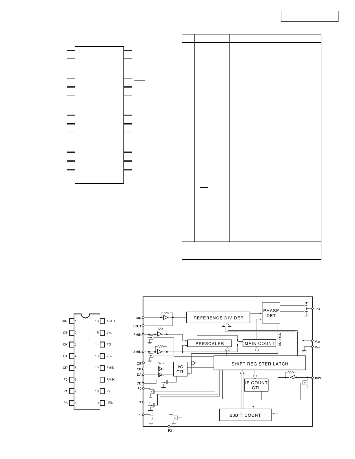
TC9246F (IC217)
VDD
LOCKS2S1
1611521431341251161079
Lock Ditection
Circuit
REF
REF
Microcomputer Interface
Programmable Counter
VAR
Phase
Comparator
PD
DDA
V
AMPI
M2
VCO
AMPO
1 TRANSISTORS
DTA114EK
DTA144EK
DTC114EK
DTC114YK
PNP
NPN
M1
VSSA
BU2090F (IC104)
CKO
Vss
Selector
8
XI
XO
B
TOP
C
VIEW
E
7Q3
8Q4
DTA Series
Control Circuit
12-Bit Shift Register
Latch
Output Buffer
(Open Drain)
C
16 VDD1Vss
15 Q112DATA
14 Q103CLOCK
13 Q94Q0
12 Q85Q1
11 Q76Q2
10 Q6
Q5
9
DTC Series
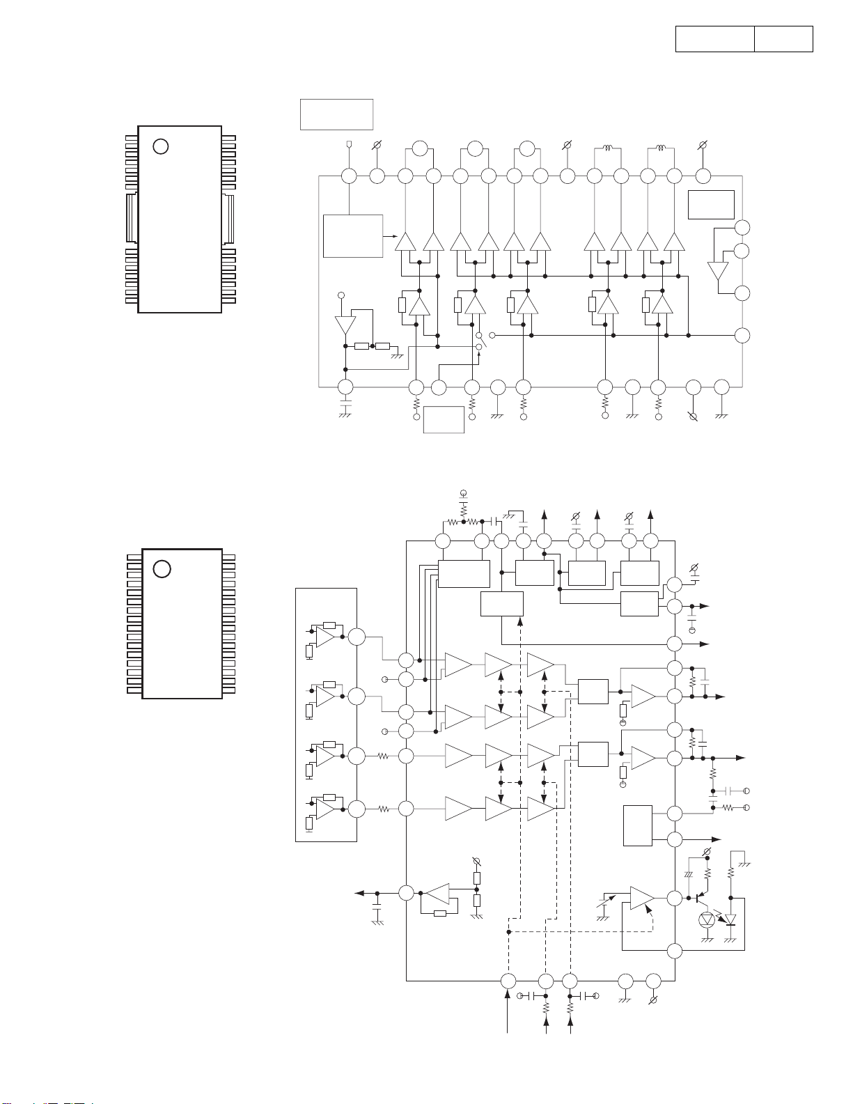
AN80L18RMS (IC208)
SW
GND
NC
5
4
3
C
1
IN
2
OUT
DTA144ES
PNP
FRONT
VIEW
C
E
B
1 OTHERS
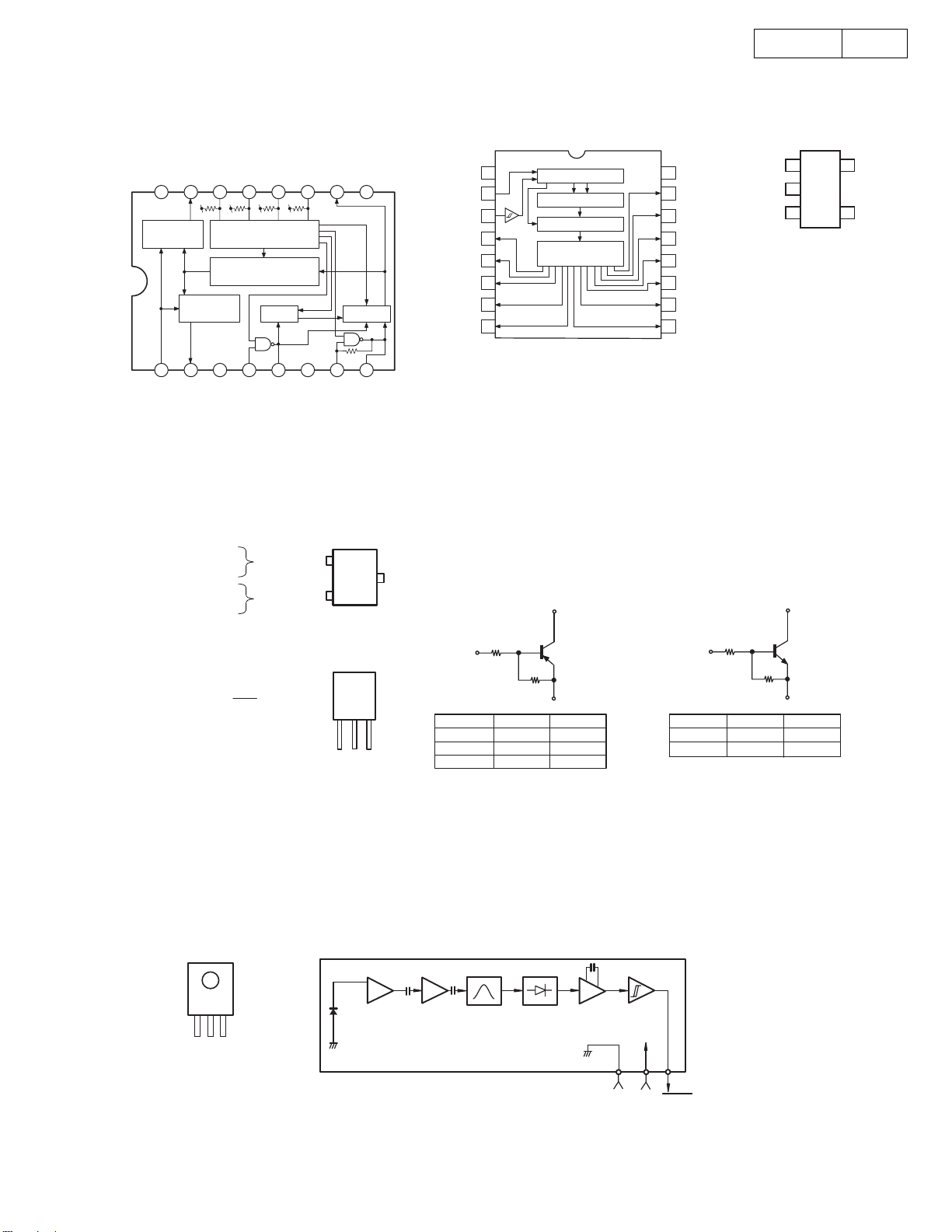
GP1UE261XK (Remote Control Sensor)
(IC501)
TOP VIEW
Head
Amp
Vcc
VOUT
GND
Limiter
Amp
R1
B
R2
R1
DTA114EK
DTA144EK
DTA144ES
10kohm
47kohm
47kohm 47kohm
Detector &
BPF Integrator
Comparator
E
R2
10kohm
47kohm
Hysteresis
Comparator
B
DTC114EK
DTC114YK
R1
R2
R1
10kohm
10kohm 47kohm
E
R2
10kohm
20
GND Vcc
VOUT
Page 21
FL DISPLAY
BJ899GN (FL501)
S1
DN-C635
21
2G 1G3G4G5G6G7G8G9G10G11G
1-1
2-1 3-1 4-1 5-1
1-2
1-3
1-4
1-5
1-6
1-7
Pin connection
Pin No.
Connection
Pin No.
Connection
1
2
3
4
F
F
N
N
1
1
P
P
5
5
5
5
3
5
6
4
N
N
N
N
P
P
P
P
Anode connection
P1
P2
P3
P4
P5
P6
P7
P8
P9
P10
P11
P12
P13
P14
P15
P16
P17
P18
P19
P20
P21
P22
P23
P24
P25
P26
P27
P28
P29
P30
P31
P32
P33
P34
P35
P36
1G~10G
1-1
2-1
3-1
4-1
5-1
1-2
2-2
3-2
4-2
5-2
1-3
2-3
3-3
4-3
5-3
1-4
2-4
3-4
4-4
5-4
1-5
2-5
3-5
4-5
5-5
1-6
2-6
3-6
4-6
5-6
1-7
2-7
3-7
4-7
5-7
-
11G
1-1
2-1
3-1
4-1
5-1
1-2
2-2
3-2
4-2
5-2
1-3
2-3
3-3
4-3
5-3
1-4
2-4
3-4
4-4
5-4
1-5
2-5
3-5
4-5
5-5
1-6
2-6
3-6
4-6
5-6
1-7
2-7
3-7
4-7
5-7
S1
S3
S2
S2
S3
1a2a
1
3
b
3
c
1
1g
f
b
1
1
e
c
1d
Dp
12G
[1G~11G] [13G]
1
1
1
1
1
1
5
6
7
8
9
0
1
I
N
C
C
5
5
7
8
P
P
2
2
8
9
N
N
N
N
N
C
C
C
C
C
5
6
6
6
6
9
0
1
2
3
P
P
P
P
P
3
3
3
3
3
0
1
2
3
4
1
2
3
4
5
6
N
N
N
N
N
C
C
C
C
C
6
6
6
6
6
6
7
8
4
5
P
P
N
N
N
3
3
C
C
C
5
6
B8
B10
B9
B7
1
1
1
2
2
2
7
8
9
2
0
1
1
N
C
N
C
N
N
P
P
3
N
G
C
C
1
C
6
7
7
7
7
7
3
9
4
0
1
2
1
2
N
N
N
G
G
C
G
C
C
B4B6
B5
2
2
2
2
3
4
5
6
P
P
P
2
3
4
5
7
7
7
7
5
6
7
8
3
4
5
6
G
G
G
B2
B1
B3
2
2
2
3
3
3
3
7
8
9
P
P
P
6
7
8
7
8
8
9
0
1
7
8
9
G
G
G
3
0
1
2
3
4
P
P
P
P
P
1
1
1
1
9
0
1
2
3
8
8
8
8
8
3
4
5
6
2
1
1
1
1
2
N
N
0
G
G
G
C
C
NOTE 1) F1,F2 : Filament
12G
13G
2) NP : No pin
3) NC : No connection
4) DL : Datum Line
5) 1G~13G : Grid
6) IC : Internal connection
S2
S3
3b,3c
2d
2e
2c
2g
2f
2b
2a
Dp
1d
1e
1c
1g
1f
1b
1a
-
-
-
B1
B2
B3
B4
B5
B6
B7
B8
B9
B10
-
13G
4
5
5
3
3
3
3
3
4
4
4
4
4
4
4
5
6
7
8
9
0
1
2
P
P
P
P
P
P
P
1
1
1
4
5
6
8
8
8
7
8
9
N
N
N
C
C
C
P
1
1
1
2
2
7
8
9
0
1
9
9
9
9
9
0
1
2
3
4
N
N
N
N
N
C
C
C
C
C
4
3
4
5
6
7
P
P
P
P
P
2
2
2
2
2
2
3
4
5
6
9
9
9
9
9
5
6
7
8
9
N
N
N
N
N
C
C
C
C
C
5
4
9
0
1
2
8
P
N
N
F
F
2
P
P
2
2
7
1
1
1
1
1
0
0
0
0
0
0
1
2
3
4
I
N
N
N
N
C
P
P
P
P
21
Page 22
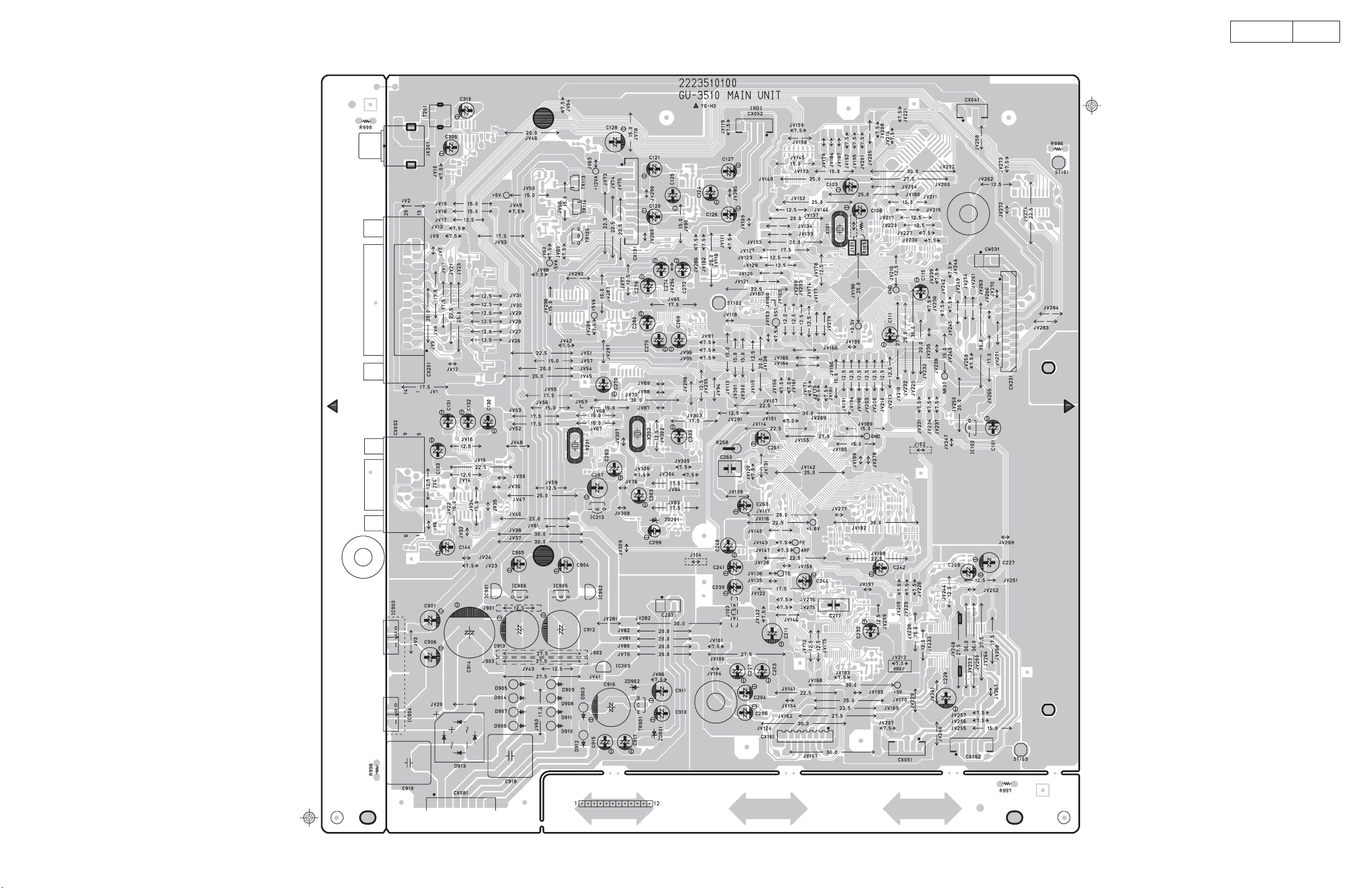
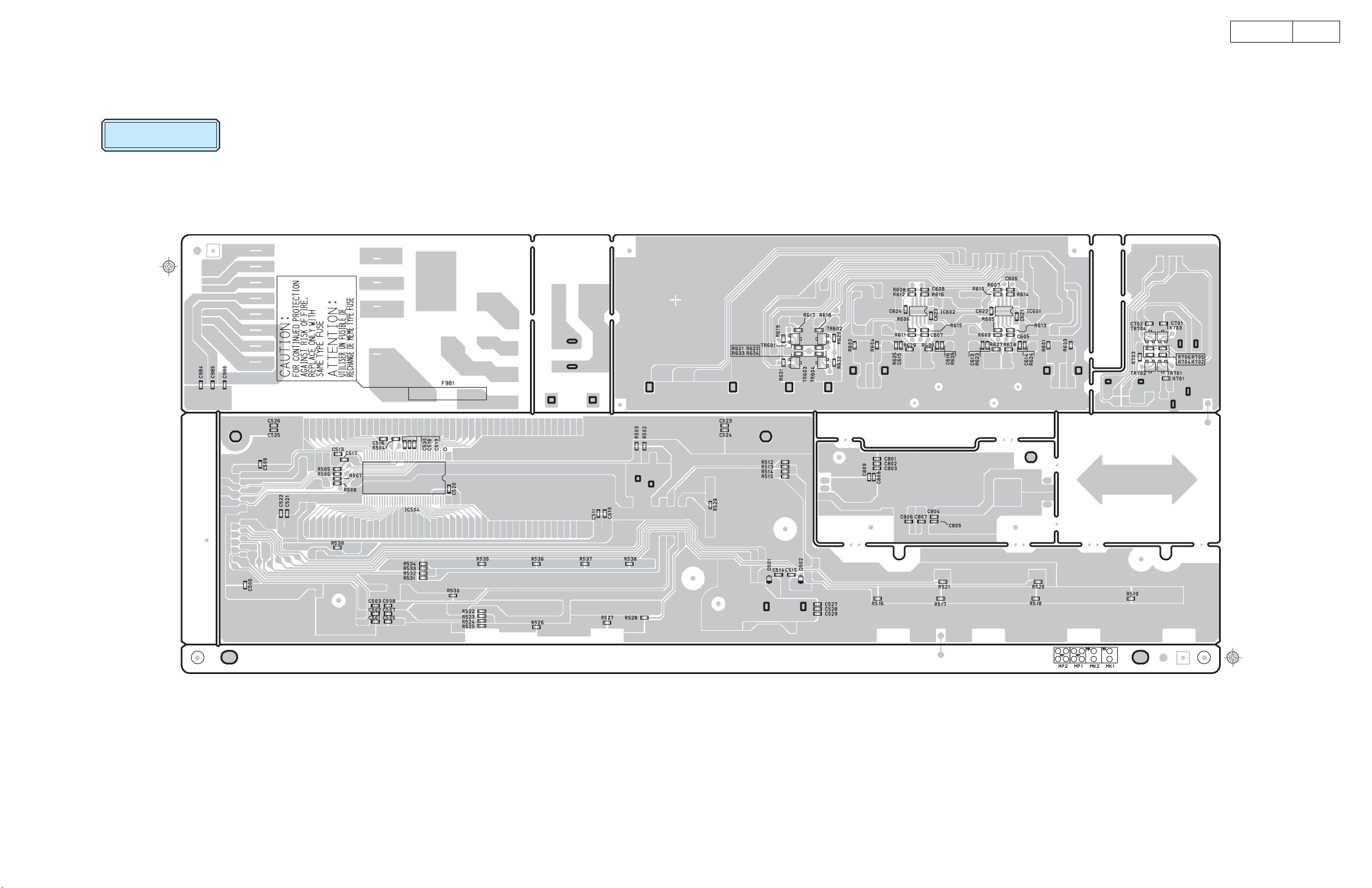
PRINTED WIRING BOARD
GU-3510 MAIN P.W.B. UNIT
DN-C635
22
22
COMPONENT SIDE
Page 23
Parts List
DN-C635
23
23
FOIL SIDE
Page 24
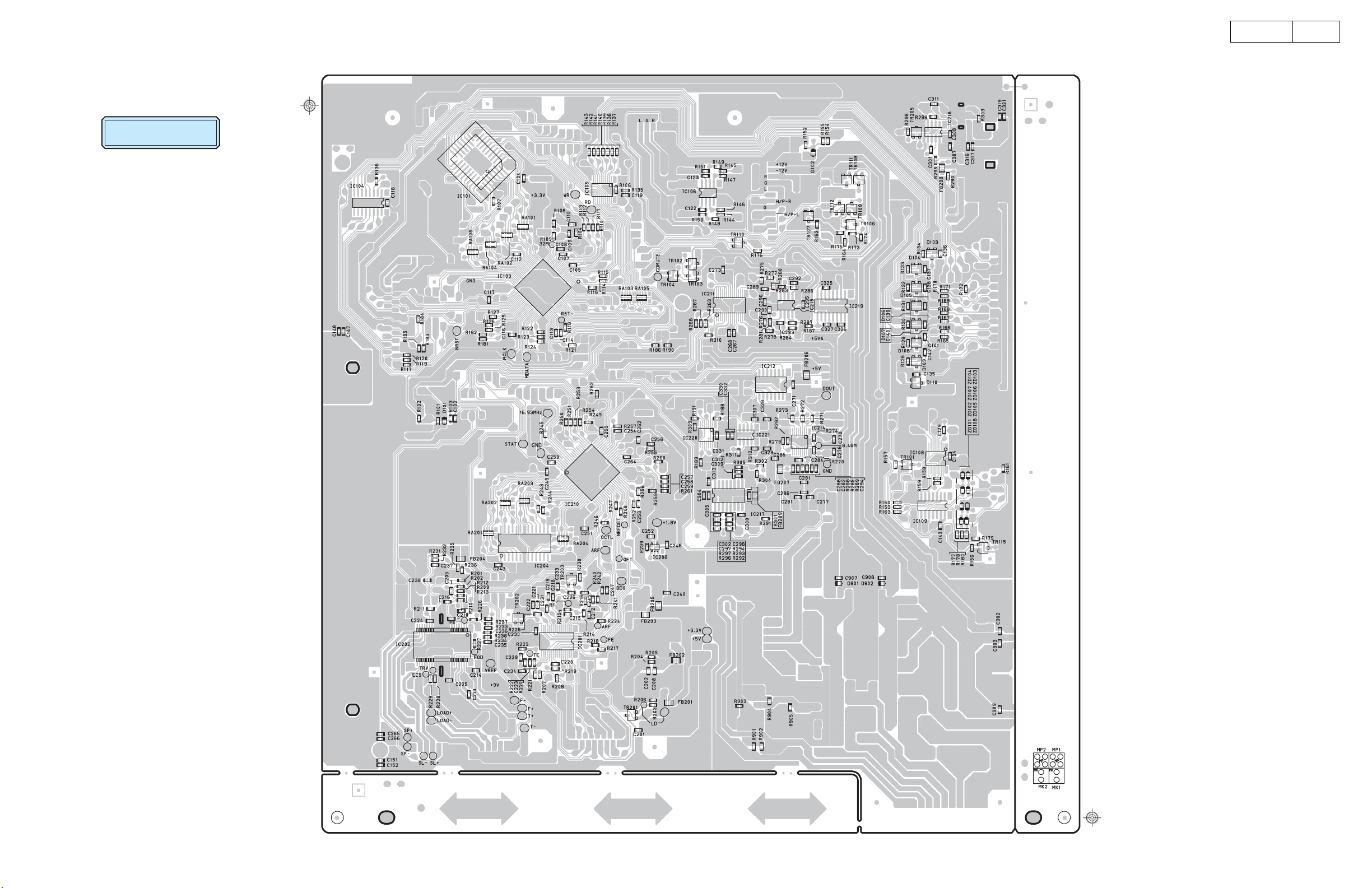
GU-3511 DISPLAY P.W.B. UNIT
Parts List
DN-C635
24
24
COMPONENT SIDE
Page 25
Parts List
DN-C635
25
25
FOIL SIDE
Page 26
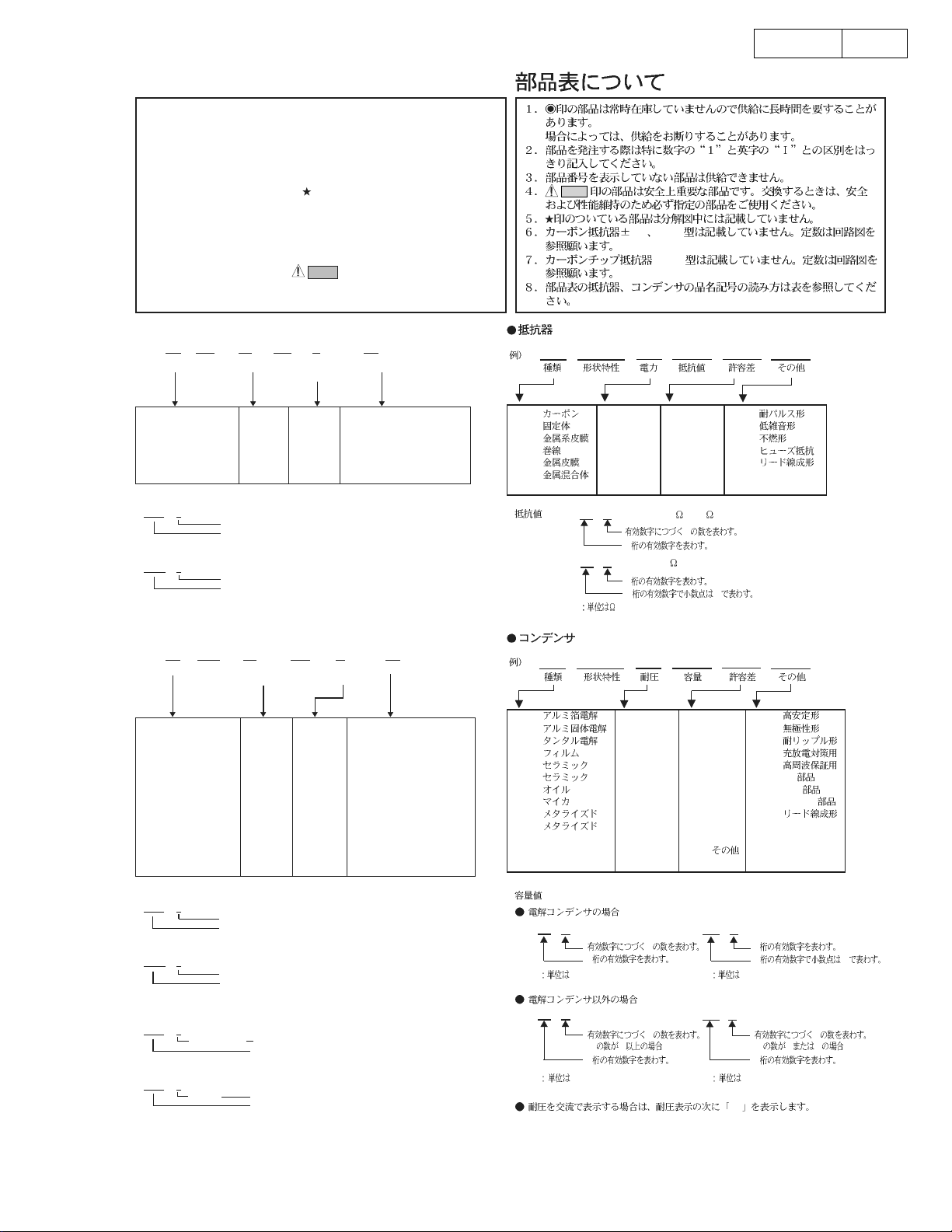
NOTE FOR PARTS LIST
l Part indicated with the mark "" are not always in stock and possibly to
take a long period of time for supplying, or in some case supplying of
part may be refused.
l When ordering of part, clearly indicate "1" and "I" (i) to avoid mis-
supplying.
l Ordering part without stating its part number can not be supplied.
l Part indicated with the mark "
l Not including Carbon Film Resister ±5%, 1/4W Type in the P.W.Board
parts list. (Refer to the Schematic Diagram for those parts.)
l Not including Carbon Chip Resister 1/16W Type in the P.W.Board parts
list. (Refer to the Schematic Diagram for those parts.)
WARNING:
Parts marked with this symbol
Use ONLY replacement parts recommended by the manufacturer.
ll
Resistors
l
ll
Ex.: RN 14K 2E 182 G FR
Type Shape Power Resist- Allowable Others
and per- ance error
formance
" is not illustrated in the exploded view.
have critical characteristics.
DN-C635
5% 1/4W
1/16W
RN 14K 2E 182 G FR
26
RD : Carbon 2B : 1/8W F : ±1% P : Pulse-resistant type
RC : Composition 2E : 1/4W G : ±2% NL : Low noise type
RS : Metal oxide film 2H : 1/2W J : ±5% NB : Non-burning type
RW : Winding 3A : 1W K : ±10% FR : Fuse-resistor
RN : Metal film 3D : 2W M : ±20% F : Lead wire forming
RK : Metal mixture 3F : 3W
] Resistance
1 8 2 ⇒ 1800 ohm = 1.8 kohm
s
s
• Units: ohm
1 R 2 ⇒ 1.2 ohm
s
s
• Units: ohm
ll
l
Capacitors
ll
Ex.: CE 04W 1H 2R2 M BP
Type Shape Dielectric Capacity Allowable Others
CE : Aluminum foil 0J : 6.3V F : ±1% HS : High stability type
electrolytic
CA : Aluminum solid 1A : 10V G : ±2% BP : Non-polar type
electrolytic
CS : Tantalum electrolytic 1C : 16V J : ±5% HR : Ripple-resistant type
CQ : Film 1E : 25V K : ±10% DL : For change and discharge
CK : Ceramic 1V : 35V M : ±20% HF : For assuring high
CC : Ceramic 1H : 50V Z : +80% U : UL part
CP : Oil 2A : 100V –20% C : CSA part
CM : Mica 2B : 125V P : +100% W : UL-CSA type
CF : Metallized 2C : 160V –0% F : Lead wire forming
CH : Metallized 2D : 200V C : ±0.25pF
3H : 5W
Indicates number of zeros after effective number.
2-digit effective number.
1-digit effective number.
2-digit effective number, decimal point indicated by R.
and per- strength error
formance
requency
2E : 250V D : ±0.5pF
2H : 500V = : Others
2J : 630V
RD : 2B : 1/8 W F : ±1% P :
RC : 2E : 1/4 W G : ±2% NL :
RS : 2H : 1/2 W J : ±5% NB :
RW : 3A : 1 W K : ±10% FR :
RN : 3D : 2 W M : ±20% F :
RK : 3F : 3 W
∗
CE 04W 1H 2R2 M BP
CE : 0J : 6.3 V F : ±1% HS :
CA : 1A : 10 V G : ±2% BP :
CS : 1C : 16 V J : ±5% HR :
CQ : 1E : 25 V K : ±10% DL :
CK : 1V : 35 V M : ±20% HF :
CC : 1H : 50 V Z : +80% U : UL
CP : 2A : 100 V −20% C : CSA
CM : 2B : 125 V P : +100% W : UL-CSA
CF : 2C : 160 V − 0% F :
CH : 2D : 200 V C : ±0.25pF
3H : 5 W
18 2
1R 2
Ö
2
Ö
1
2 R
2E : 250 V D : ±0.5pF
2H : 500 V = :
2J : 630 V
1800
1.2
=1.8k
0
] Capacity (electrolyte only)
2 2 2 ⇒ 2200µF
s
s
• Units: µF.
2 R 2 ⇒ 2.2µF
s
s
• Units: µF.
] Capacity (except electrolyte)
2 2 2 ⇒ 2200pF=0.0022µF
s
s
• Units: pF.
2 2 1 ⇒ 220pF
s
s
• Units: pF.
• When the dielectric strength is indicated in AC, "AC" is included after the dieelectric
strength value.
Indicates number of zeros after effective number.
2-digit effective number.
1-digit effective number.
2-digit effective number, decimal point indicated by R.
(More than 2) Indicates number of zeros after effective number.
(0 or 1) Indicates number of zeros after effective number.
2-digit effective number.
2-digit effective number.
26
∗
22 2
µ
22 2
p
2200µF
Ö
2
F
2200pF=0.0022µF
Ö
(0 2 )
2
F
0
0
2R 2
µ
22 1
p
Ö
1
2 R
F
Ö
(0 0 1 )
2
F
AC
2.2µF
220pF
0
Page 27

PARTS LIST OF P.W.B. UNIT
Note: The symbols in the column "Remarks" indicate the following destinations.
E3: U.S.A./Canada model E2K: Korea model
E2: Europe model JP: Japan model
00DGU-3510 MAIN P.W.B. UNIT ASS'Y
Ref. No. Part No. Part Name Remarks Q'ty New
SEMICONDUCTORS GROUP
IC101 00D GEN 6322 DNC635 SYSTEM ROM 4M FLASH MEM.(PLCC)
IC102 00D 263 0913 905 PST600C TP
IC103 00D 262 3171 000 MN102H60KDA +C
IC104 00D 262 2745 903 BU2090F(E2) +C
IC105 00D 262 2641 900 SN74LV541APW-EL2 +C
IC106 00D 263 0615 902 BA15218F-DXE2 +C
IC108 00D 262 3172 902 MAX3221CAE-T +C
IC109 00D 262 3173 901 SN75LBC180DR +C
IC201 00D 262 3160 901 AN22002A
IC202 00D 262 3159 909 AN8785SB
IC204 00D 262 2881 003 16M DRAM(3.3V)
IC208 00D 263 1178 901 AN80L20RMSTX
IC210 00D 262 3158 007 MN6627911AC
IC211 00D 262 2490 902 PCM1716E(TAPE) +C
IC212 00D 262 2376 903 TC74HCT7007AF(TP1) +C
IC213 00D 263 0432 907 NJM78L05AT
IC214 00D 262 2651 903 BU2618FV(E2) +C
IC215 00D 263 0615 902 BA15218F-DXE2 +C
IC217 00D 262 1883 905 TC9246F-TP1 +C
IC218 00D 262 1953 903 TC7WU04F +C
IC219 00D 262 0707 901 TC4053BF (TAPE) +C
IC220 00D 262 2519 906 SN74LV00APW-EL2 +C
IC221 00D 262 1953 903 TC7WU04F +C
IC903 00D 263 1048 002 BA033T
IC904 00D 263 0800 005 NJM78M05FA(S)
IC905 00D 263 0432 907 NJM78L05AT
IC906 00D 263 0722 905 NJM79L05AT
27DN-C635
TR101,102 00D 269 0082 902 DTC114EKT96 +C
TR103 00D 269 0083 901 DTA114EKT96 +C
TR104 00D 269 0082 902 DTC114EKT96 +C
TR105 00D 275 0042 905 2SK373(Y)TPE2
TR106 00D 269 0055 900 DTA144EKT96 +C
TR107 00D 269 0082 902 DTC114EKT96 +C
TR108,109 00D 269 0083 901 DTA114EKT96 +C
TR110-112 00D 269 0082 902 DTC114EKT96 +C
TR113,114 00D 269 0093 904 DTA144ES (47K-47K) T
TR115 00D 269 0055 900 DTA144EKT96 +C
TR201 00D 272 0125 904 2SB709A +C
TR202,203 00D 269 0144 905 DTC114YK-T146 +C
TR205 00D 273 0460 905 KTC2875B-RTK +C
TR901 00D 272 0025 907 2SB562(C)TF
D101,102 00D 276 0717 903 1SS355 TE-17 +C
D103-110 00D 276 0529 900 MA157A-TX +C
27
Page 28

Ref. No. Part No. Part Name Remarks Q'ty New
D901,902 00D 276 0717 903 1SS355 TE-17 +C
D903,904 00D 276 0550 908 1SR139-200T-62
D906 00D 276 0550 908 1SR139-200T-62
D908 00D 276 0550 908 1SR139-200T-62
D910 00D 276 0550 908 1SR139-200T-62
D912 00D 276 0550 908 1SR139-200T-62
D913 00D 276 0338 007 S4VB20F
ZD101-108 00D 276 0692 905 RD24SB-T1 +C
ZD201 00D 276 0450 901 HZS2B-1TD
ZD901 00D 276 0643 983 MTZJ5.1A T77
ZD902 00D 276 0762 929 MTZJ30B T77
RESISTORS GROUP
R101,102 00D 247 2007 943 RM73B--102JT +1608
R103 00D 247 2018 903 RM73B--0R0KT +1608
R104 00D 247 2011 942 RM73B--473JT +1608
R106,107 00D 247 2011 942 RM73B--473JT +1608
R108 00D 247 2018 903 RM73B--0R0KT +1608
R110-115 00D 247 2003 989 RM73B--330JT +1608
R116,117 00D 247 2011 942 RM73B--473JT +1608
R118 00D 247 2009 983 RM73B--103JT +1608
R119,120 00D 247 2011 942 RM73B--473JT +1608
R121 00D 247 2003 989 RM73B--330JT +1608
R122-126 00D 247 2011 942 RM73B--473JT +1608
R127 00D 247 2009 983 RM73B--103JT +1608
R128-135 00D 247 2011 942 RM73B--473JT +1608
R136-143 00D 247 2003 989 RM73B--330JT +1608
R144-147 00D 247 2011 942 RM73B--473JT +1608
R148,149 00D 247 2009 967 RM73B--822JT +1608
R150,151 00D 247 2008 968 RM73B--332JT +1608
R152 00D 247 2005 903 RM73B--101JT +1608
R153 00D 247 2009 983 RM73B--103JT +1608
R154,155 00D 247 2009 912 RM73B--512JT +1608
R156,157 00D 247 2009 983 RM73B--103JT +1608
R158 00D 247 2018 903 RM73B--0R0KT +1608
R160 00D 247 2008 955 RM73B--302JT +1608
R161 00D 247 2007 927 RM73B--821JT +1608
R163 00D 247 2007 998 RM73B--162JT +1608
R164 00D 247 2017 904 RM73B--106KT +1608
R165-172 00D 247 2009 909 RM73B--472JT (1608) +1608
R173,174 00D 247 2015 948 RM73B--225KT +1608
R175 00D 247 2012 925 RM73B--104JT +1608
R176 00D 247 2011 942 RM73B--473JT +1608
R179 00D 247 2007 927 RM73B--821JT +1608
R180 00D 247 2005 903 RM73B--101JT +1608
R181,182 00D 247 2018 903 RM73B--0R0KT +1608
R183-186 00D 247 2009 983 RM73B--103JT +1608
R187 00D 247 2007 943 RM73B--102JT +1608
28DN-C635
28
Page 29

Ref. No. Part No. Part Name Remarks Q'ty New
R188,189 00D 247 2003 989 RM73B--330JT +1608
R190 00D 247 2009 983 RM73B--103JT +1608
R191 00D 247 2005 961 RM73B--181JT +1608
R201 00D 247 2009 925 RM73B--562JT +1608
R202 00D 247 2009 983 RM73B--103JT +1608
R203 00D 247 2001 981 RM73B--4R7KT +1608
R204,205 00D 247 2004 991 RM73B--910JT +1608
R206 00D 247 2011 926 RM73B--393JT +1608
R207,208 00D 247 2009 967 RM73B--822JT +1608
R209,210 00D 247 2012 925 RM73B--104JT +1608
R211 00D 247 2009 983 RM73B--103JT +1608
R212,213 00D 247 2012 925 RM73B--104JT +1608
R214 00D 247 2008 955 RM73B--302JT +1608
R215 00D 247 2007 969 RM73B--122JT +1608
R216 00D 247 2006 986 RM73B--561JT +1608
R217 00D 247 2018 903 RM73B--0R0KT +1608
R218 00D 247 2009 941 RM73B--682JT +1608
R219 00D 247 2010 956 RM73B--203JT +1608
R220 00D 247 2011 997 RM73B--753JT +1608
R221 00D 247 2018 903 RM73B--0R0KT +1608
R223,224 00D 247 2018 903 RM73B--0R0KT +1608
R225 00D 247 2014 949 RM73B--824JT +1608
R226,227 00D 247 2008 984 RM73B--392JT +1608
R228,229 00D 247 2009 983 RM73B--103JT +1608
R230 00D 247 2013 940 RM73B--334JT +1608
R231 00D 247 2010 927 RM73B--153JT +1608
R232 00D 247 2010 969 RM73B--223JT +1608
R233 00D 247 2011 926 RM73B--393JT +1608
R234 00D 247 2010 927 RM73B--153JT +1608
R235,236 00D 247 2009 925 RM73B--562JT +1608
R237 00D 247 2007 943 RM73B--102JT +1608
R238 00D 247 2009 925 RM73B--562JT +1608
R239 00D 247 2010 985 RM73B--273JT +1608
R240 00D 247 2018 903 RM73B--0R0KT +1608
R241,242 00D 247 2012 925 RM73B--104JT +1608
R243,244 00D 247 2003 989 RM73B--330JT +1608
R245 00D 247 2010 985 RM73B--273JT +1608
R246 00D 247 2010 901 RM73B--123JT +1608
R247,248 00D 247 2008 968 RM73B--332JT +1608
R249 00D 247 2011 900 RM73B--333JT +1608
R250,251 00D 247 2005 903 RM73B--101JT +1608
R252 00D 247 2009 925 RM73B--562JT +1608
R253,254 00D 247 2005 903 RM73B--101JT +1608
R255,256 00D 247 2010 972 RM73B--243JT +1608
R257 00D 247 2010 985 RM73B--273JT +1608
R258 00D 244 2043 937 RS14B3A100JNBST(S)
R259 00D 247 2010 927 RM73B--153JT +1608
R260 00D 247 2006 986 RM73B--561JT +1608
R261 00D 247 2010 927 RM73B--153JT +1608
R262 00D 247 2005 903 RM73B--101JT +1608
R263 00D 247 2003 989 RM73B--330JT +1608
R267,268 00D 247 2003 989 RM73B--330JT +1608
29DN-C635
29
Page 30

Ref. No. Part No. Part Name Remarks Q'ty New
R270 00D 247 2018 903 RM73B--0R0KT +1608
R271-273 00D 247 2005 903 RM73B--101JT +1608
R274 00D 247 2014 965 RM73B--105JT +1608
R275,276 00D 247 2011 942 RM73B--473JT +1608
R277-281 00D 247 2009 983 RM73B--103JT +1608
R283,284 00D 247 2009 983 RM73B--103JT +1608
R285 00D 247 2009 925 RM73B--562JT +1608
R286,287 00D 247 2009 983 RM73B--103JT +1608
R288,289 00D 247 2012 925 RM73B--104JT +1608
R290 00D 247 2005 987 RM73B--221JT +1608
R291 00D 247 2012 912 RM73B--913JT +1608
R292 00D 247 2012 983 RM73B--184JT +1608
R293 00D 247 2005 903 RM73B--101JT +1608
R294 00D 247 2013 937 RM73B--304JT +1608
R295 00D 247 2006 960 RM73B--471JT +1608
R296 00D 247 2008 939 RM73B--242JT +1608
R297 00D 247 2009 912 RM73B--512JT +1608
R298 00D 247 2010 956 RM73B--203JT +1608
R299 00D 247 2014 965 RM73B--105JT +1608
R302 00D 247 2004 920 RM73B--470JT +1608
R303 00D 247 2004 975 RM73B--750JT +1608
R304 00D 247 2007 943 RM73B--102JT +1608
R307 00D 247 2014 965 RM73B--105JT +1608
R309 00D 247 2006 944 RM73B--391JT +1608
R310 00D 247 2004 920 RM73B--470JT +1608
R311 00D 247 2018 903 RM73B--0R0KT +1608
R312 00D 247 2007 901 RM73B--681JT +1608
R901,902 00D 247 2005 903 RM73B--101JT +1608
R903 00D 247 2011 942 RM73B--473JT +1608
R904 00D 247 2008 968 RM73B--332JT +1608
R905 00D 247 2012 925 RM73B--104JT +1608
30DN-C635
RA101-106 00D 247 9002 909 MNR14=330JE0AB +C
RA201-204 00D 247 9002 909 MNR14=330JE0AB +C
CAPACITORS GROUP
C101 00D 254 4538 900 CE04W1C100MT SMG/RE3
C102 00D 257 0509 929 CK73B1H102KT +1608
C103 00D 254 4536 915 CE04W1A470MT SMG/RE3
C104,105 00D 257 0512 903 CK73F1E104ZT +1608
C106 00D 254 4533 921 CE04W0J101MT SMG/RE3
C107 00D 257 0511 904 CK73F1H103ZT +1608
C108 00D 257 0512 903 CK73F1E104ZT +1608
C109 00D 257 0503 912 CC73CH1H9R0DT +1608
C110 00D 257 0503 925 CC73CH1H100DT +1608
C111 00D 254 4533 921 CE04W0J101MT SMG/RE3
C112 00D 257 0512 903 CK73F1E104ZT +1608
C113 00D 257 0511 904 CK73F1H103ZT +1608
C114 00D 257 0512 903 CK73F1E104ZT +1608
30
Page 31

Ref. No. Part No. Part Name Remarks Q'ty New
C115 00D 254 4533 921 CE04W0J101MT SMG/RE3
C116-119 00D 257 0512 903 CK73F1E104ZT +1608
C120,121 00D 254 4536 915 CE04W1A470MT SMG/RE3
C122,123 00D 257 0506 951 CC73CH1H101JT +1608
C124,125 00D 254 4533 921 CE04W0J101MT SMG/RE3
C126,127 00D 254 4538 900 CE04W1C100MT SMG/RE3
C128 00D 254 4538 955 CE04W1C221MT SMG/RE3
C129 00D 257 0517 908 CK73B1C473KT +1608
C130 00D 254 4524 930 CE04W1HR47MT SMG/RE3
C131,132 00D 254 4524 927 CE04W1HR33MT SMG/RE3
C133 00D 254 4538 900 CE04W1C100MT SMG/RE3
C134 00D 257 0512 903 CK73F1E104ZT +1608
C135-142 00D 257 0511 904 CK73F1H103ZT +1608
C143 00D 257 0512 903 CK73F1E104ZT +1608
C144 00D 254 4538 900 CE04W1C100MT SMG/RE3
C147 00D 257 0512 903 CK73F1E104ZT +1608
C148 00D 257 0511 904 CK73F1H103ZT +1608
C202 00D 257 0512 903 CK73F1E104ZT +1608
C203 00D 254 4524 969 CE04W1H3R3MT SMG/RE3
C204 00D 254 4536 915 CE04W1A470MT SMG/RE3
C205 00D 257 0512 903 CK73F1E104ZT +1608
C206 00D 254 4536 915 CE04W1A470MT SMG/RE3
C207 00D 254 4533 921 CE04W0J101MT SMG/RE3
C208 00D 257 0512 903 CK73F1E104ZT +1608
C209 00D 254 4538 939 CE04W1C470MT SMG/RE3
C210 00D 257 0512 903 CK73F1E104ZT +1608
C211 00D 254 4536 957 CE04W1A471MT SMG/RE3
C212 00D 257 0512 903 CK73F1E104ZT +1608
C216 00D 257 0512 903 CK73F1E104ZT +1608
C217 00D 256 1059 912 CF93A1H224JT (JL)
C218 00D 257 0512 903 CK73F1E104ZT +1608
C219 00D 257 0501 914 CK73B1H123KT +1608
C220 00D 257 0507 950 CC73CH1H271JT +1608
C221 00D 257 0510 947 CK73B1H562KT +1608
C222 00D 257 0516 909 CK73B1E223KT +1608
C223 00D 257 0506 993 CC73CH1H151JT +1608
C224,225 00D 257 0512 903 CK73F1E104ZT +1608
C226 00D 257 0506 935 CC73CH1H820JT +1608
C227,228 00D 254 4538 955 CE04W1C221MT SMG/RE3
C230 00D 257 0512 903 CK73F1E104ZT +1608
C231 00D 257 0501 927 CK73B1H153KT +1608
C232 00D 254 4533 921 CE04W0J101MT SMG/RE3
C233 00D 257 0506 948 CC73CH1H910JT +1608
C235-238 00D 257 0509 990 CK73B1H222KT +1608
C239 00D 254 4533 921 CE04W0J101MT SMG/RE3
C240 00D 257 0512 903 CK73F1E104ZT +1608
C241 00D 254 4538 900 CE04W1C100MT SMG/RE3
C242 00D 254 4533 921 CE04W0J101MT SMG/RE3
C243 00D 257 0513 902 CK73F1A105ZT +1608
C244 00D 254 4538 900 CE04W1C100MT SMG/RE3
C245 00D 257 0516 909 CK73B1E223KT +1608
C246 00D 257 0512 903 CK73F1E104ZT +1608
31DN-C635
31
Page 32

Ref. No. Part No. Part Name Remarks Q'ty New
C247 00D 257 0516 909 CK73B1E223KT +1608
C248 00D 254 4538 900 CE04W1C100MT SMG/RE3
C249-252 00D 257 0512 903 CK73F1E104ZT +1608
C253 00D 257 0509 929 CK73B1H102KT +1608
C254-256 00D 257 0512 903 CK73F1E104ZT +1608
C257 00D 257 0509 929 CK73B1H102KT +1608
C258 00D 257 0516 909 CK73B1E223KT +1608
C259 00D 257 0512 903 CK73F1E104ZT +1608
C260 00D 256 1058 984 CF93A1H124JT (JL)
C261 00D 254 4536 915 CE04W1A470MT SMG/RE3
C262 00D 257 0512 903 CK73F1E104ZT +1608
C263 00D 254 4533 934 CE04W0J221MT SMG/RE3
C264 00D 257 0512 903 CK73F1E104ZT +1608
C267 00D 257 0511 904 CK73F1H103ZT +1608
C268 00D 257 0512 903 CK73F1E104ZT +1608
C269 00D 254 4538 900 CE04W1C100MT SMG/RE3
C270 00D 254 4536 915 CE04W1A470MT SMG/RE3
C271 00D 257 0512 903 CK73F1E104ZT +1608
C272 00D 254 4538 900 CE04W1C100MT SMG/RE3
C273 00D 257 0512 903 CK73F1E104ZT +1608
C274,275 00D 254 4538 900 CE04W1C100MT SMG/RE3
C276 00D 257 0503 967 CC73CH1H150JT +1608
C277 00D 257 0512 903 CK73F1E104ZT +1608
C278 00D 257 0503 967 CC73CH1H150JT +1608
C279,280 00D 254 4538 900 CE04W1C100MT SMG/RE3
C281 00D 257 0512 903 CK73F1E104ZT +1608
C282 00D 257 0511 904 CK73F1H103ZT +1608
C283 00D 254 4533 921 CE04W0J101MT SMG/RE3
C284 00D 257 0511 904 CK73F1H103ZT +1608
C285,286 00D 257 0512 903 CK73F1E104ZT +1608
C287 00D 254 4536 944 CE04W1A331MT SMG/RE3
C288 00D 257 0512 903 CK73F1E104ZT +1608
C289,290 00D 257 0507 976 CC73CH1H331JT +1608
C291 00D 257 0511 904 CK73F1H103ZT +1608
C292,293 00D 257 0507 976 CC73CH1H331JT +1608
C294 00D 257 0507 992 CC73CH1H391JT +1608
C295,296 00D 257 0512 903 CK73F1E104ZT +1608
C297 00D 257 0506 951 CC73CH1H101JT +1608
C299 00D 254 4305 955 CE04W1HR68MT(SRE)
C301 00D 257 0509 929 CK73B1H102KT +1608
C302 00D 257 0512 903 CK73F1E104ZT +1608
C303 00D 254 4533 934 CE04W0J221MT SMG/RE3
C304 00D 257 0512 903 CK73F1E104ZT +1608
C305 00D 257 0511 904 CK73F1H103ZT +1608
C306 00D 254 4533 921 CE04W0J101MT SMG/RE3
C307 00D 257 0501 901 CK73B1H103KT (1608) +1608
C308,309 00D 257 0512 903 CK73F1E104ZT +1608
C310 00D 254 4538 926 CE04W1C330MT SMG/RE3
C311 00D 257 0501 901 CK73B1H103KT (1608) +1608
C313 00D 257 0512 903 CK73F1E104ZT +1608
C316 00D 257 0501 901 CK73B1H103KT (1608) +1608
C317 00D 257 0512 903 CK73F1E104ZT +1608
32DN-C635
32
Page 33

Ref. No. Part No. Part Name Remarks Q'ty New
C321 00D 257 0512 903 CK73F1E104ZT +1608
C325-327 00D 257 0512 903 CK73F1E104ZT +1608
C328,329 00D 257 0503 983 CC73CH1H180JT +1608
C330 00D 257 0509 929 CK73B1H102KT +1608
C331,332 00D 257 0512 903 CK73F1E104ZT +1608
C333 00D 254 4533 921 CE04W0J101MT SMG/RE3
C901 00D 254 4536 957 CE04W1A471MT SMG/RE3
C902,903 00D 257 0512 903 CK73F1E104ZT +1608
C904,905 00D 254 4536 928 CE04W1A101MT SMG/RE3
C906 00D 254 4536 957 CE04W1A471MT SMG/RE3
C907-909 00D 257 0512 903 CK73F1E104ZT +1608
C910 00D 254 4524 985 CE04W1H100MT SMG/RE3
C911 00D 254 4525 913 CE04W1H470MT SMG/RE3
C912,913 00D 254 4569 717 CE04W1E222MC (RA3)
C914 00D 254 4472 707 CE04W1C472MC (SMG)
C916 00D 254 4525 751 CE04W1H471MC SMG/RE3
OTHERS PARTS GROUP
33DN-C635
CW031 00D 203 5308 018 3P DA-DA CON CORD *
CX041 00D 205 0343 045 4P CONN.BASE(KR-PH)
CX051 00D 205 0343 058 5P CONN.BASE(KR-PH)
CX052 00D 205 0321 054 5P CONNE.BASE (RED)
CX062 00D 205 0343 061 6P CONN.BASE(KR-PH)
CX081 00D 205 0233 087 8P EH CON BASE
CX092 00D 205 1243 005 9P DSUB KIT
CX131 00D 205 0375 039 13P CONN.BASE(KR-PH)
CX161 00D 205 0892 033 16P FFC BASE (P=1)
CX231 00D 205 0880 003 23P FFC CON.BASE
CX251 00D 205 1244 004 25P DSUB KIT
FB201-203 00D 235 0106 908 CHIP EMIFIL (21A05) +C
FB205-209 00D 235 0106 908 CHIP EMIFIL (21A05) +C
JK201 00D 204 8593 001 1P PIN JACK(OR,NI)
ST101-103 00D 205 0452 017 STYLE PIN
T201 00D 231 8063 009 PULSE TRANS
X101 00D 399 0794 009 X'TAL (32.00M)
X201 00D 399 0595 004 XTAL(8.4672MHZ)
X202 00D 399 0165 007 XTAL (16.9344)
00D 417 0401 001 RADIATOR
0RD 477 0153 018 3X16 CPTS(B) SW W
33
Page 34

00DGU-3511/3511A/3511B DISPLAY P.W.B. UNIT ASS'Y
Ref. No. Part No. Part Name Remarks Q'ty New
SEMICONDUCTORS GROUP
IC501 00D 499 0305 002 GP1UE261XK *
IC504 00D 262 3228 908 M66005AFP +C
IC601,602 00D 263 0615 902 BA15218F-DXE2 +C
TR601-604 00D 273 0460 905 KTC2875B-RTK +C
TR701,702 00D 273 0460 905 KTC2875B-RTK +C
D501,502 00D 276 0717 903 1SS355 TE-17 +C
LD501 00D 393 9543 923 SLR-325DC (ORG) TAPE
LD502-504 00D 393 9543 910 SLR-325MC (GRN) TAPE
RESISTORS GROUP
34DN-C635
R502 00D 247 2004 920 RM73B--470JT +1608
R503 00D 247 2009 983 RM73B--103JT +1608
R504 00D 247 2010 985 RM73B--273JT +1608
R505 00D 247 2009 983 RM73B--103JT +1608
R506,507 00D 247 2006 902 RM73B--331JT (1608) +1608
R508 00D 247 2009 983 RM73B--103JT +1608
R512 00D 247 2007 943 RM73B--102JT +1608
R513 00D 247 2005 945 RM73B--151JT +1608
R514 00D 247 2005 961 RM73B--181JT +1608
R515 00D 247 2006 915 RM73B--271JT +1608
R516 00D 247 2006 944 RM73B--391JT +1608
R517 00D 247 2007 901 RM73B--681JT +1608
R518 00D 247 2007 972 RM73B--132JT +1608
R519 00D 247 2008 984 RM73B--392JT +1608
R520 00D 247 2006 915 RM73B--271JT +1608
R521 00D 247 2005 932 RM73B--131JT +1608
R522 00D 247 2007 943 RM73B--102JT +1608
R523 00D 247 2005 945 RM73B--151JT +1608
R524 00D 247 2005 961 RM73B--181JT +1608
R525 00D 247 2006 915 RM73B--271JT +1608
R526 00D 247 2006 944 RM73B--391JT +1608
R527 00D 247 2007 901 RM73B--681JT +1608
R528 00D 247 2007 972 RM73B--132JT +1608
R529 00D 247 2008 984 RM73B--392JT +1608
R530 00D 247 2005 932 RM73B--131JT +1608
R531 00D 247 2007 943 RM73B--102JT +1608
R532 00D 247 2005 945 RM73B--151JT +1608
R533 00D 247 2005 961 RM73B--181JT +1608
R534 00D 247 2006 915 RM73B--271JT +1608
R535 00D 247 2006 944 RM73B--391JT +1608
R536 00D 247 2007 901 RM73B--681JT +1608
R537 00D 247 2007 972 RM73B--132JT +1608
R538 00D 247 2008 984 RM73B--392JT +1608
34
Page 35

Ref. No. Part No. Part Name Remarks Q'ty New
R539 00D 247 2005 932 RM73B--131JT +1608
R601,602 00D 247 2012 925 RM73B--104JT +1608
R603,604 00D 247 2004 946 RM73B--560JT +1608
R605,606 00D 247 2011 997 RM73B--753JT +1608
R607-609 00D 247 2009 983 RM73B--103JT +1608
R610 00D 247 2012 925 RM73B--104JT +1608
R611 00D 247 2009 983 RM73B--103JT +1608
R612 00D 247 2012 925 RM73B--104JT +1608
R613 00D 247 2010 956 RM73B--203JT +1608
R614 00D 247 2010 998 RM73B--303JT +1608
R615 00D 247 2010 956 RM73B--203JT +1608
R616 00D 247 2010 998 RM73B--303JT +1608
R617,618 00D 247 2012 925 RM73B--104JT +1608
R619,620 00D 247 2005 945 RM73B--151JT +1608
R621,622 00D 247 2009 983 RM73B--103JT +1608
R623-626 00D 247 2010 956 RM73B--203JT +1608
R627-630 00D 247 2004 920 RM73B--470JT +1608
R631,632 00D 247 2005 945 RM73B--151JT +1608
R633,634 00D 247 2009 983 RM73B--103JT +1608
R701 00D 247 2004 946 RM73B--560JT +1608
R702 00D 247 2009 983 RM73B--103JT +1608
R703 00D 247 2004 946 RM73B--560JT +1608
R704 00D 247 2009 983 RM73B--103JT +1608
35DN-C635
VR601,602 00D 211 0552 019 V09QB103 *
VR701 00D 211 0906 005 V0920V17FA202K
VR801 00D 211 0908 003 SLIDE VOLUME
CAPACITORS GROUP
C501 00D 257 0511 920 CK73F1H473ZT +1608
C504 00D 254 4300 963 CE04W0J101MT(SRE)
C506 00D 257 0512 903 CK73F1E104ZT +1608
C510,511 00D 257 0511 920 CK73F1H473ZT +1608
C512 00D 254 4300 947 CE04W0J470MT(SRE)
C513 00D 257 0511 920 CK73F1H473ZT +1608
C516 00D 257 0506 951 CC73CH1H101JT +1608
C517 00D 257 0512 903 CK73F1E104ZT +1608
C518 00D 257 0509 929 CK73B1H102KT +1608
C519,520 00D 257 0512 903 CK73F1E104ZT +1608
C521,522 00D 257 0511 920 CK73F1H473ZT +1608
C601-604 00D 254 4538 900 CE04W1C100MT SMG/RE3
C605 00D 257 0503 970 CC73CH1H160JT +1608
C606 00D 257 0503 909 CC73CH1H8R0DT +1608
C607 00D 257 0503 970 CC73CH1H160JT +1608
C608 00D 257 0503 909 CC73CH1H8R0DT +1608
C609-612 00D 254 4522 958 CE04W1V101MT SMG/RE3
C613-616 00D 257 0509 929 CK73B1H102KT +1608
C621-624 00D 257 0512 903 CK73F1E104ZT +1608
C701,702 00D 257 0511 904 CK73F1H103ZT +1608
35
Page 36

Ref. No. Part No. Part Name Remarks Q'ty New
C804 00D 257 0512 903 CK73F1E104ZT +1608
C805-807 00D 257 0511 904 CK73F1H103ZT +1608
! C983 00D 253 8022 707 CK45F2EAC103MC
OTHERS PARTS GROUP
CW041 00D 203 6181 098 4P KR-DS CON CORD
CW052 00D 203 8224 047 5P PH-SAN CON.CORD *
CW081 00D 204 2451 042 8P EH-SCN CON.CORD *
CW131 00D 204 6253 026 13P KR-DA CON CORD
CX021 00D 205 0581 001 2P VH CONNECTOR BASE
CX022 00D 205 0768 002 2P VH CON.BASE (BLK)
CY022 00D 205 0453 016 2P VH CONN BASE(L)
CY231 00D 205 1052 005 23P FFC BASE (9604F)
36DN-C635
! F981 00D 206 1087 086 FUSE (ET0.315A) for E3, JP *
! F981 00D 206 1087 060 FUSE (ET0.2A) for E2, E2K *
FF981 00D 202 0040 909 FUSE CLIP(TAPE)
FH981 00D 202 0040 909 FUSE CLIP(TAPE)
FL501 00D 393 8088 007 FL TUBE(BN019GNS) *
JK601 00D 204 8553 009 2P PIN JACK (FG-ANA)
JK602 00D 204 8663 009 4P PIN JACK(SLD BK)
JK606,607 00D 205 1255 006 XLR OUT (JY-5032A)
JK701 00D 204 8264 097 H/P JACK (AU) *
L981 00D 235 0159 007 PLH10AN3711ROP2B
S501 00D 212 0410 002 ROTARY ENCODER-JOG SWITCH
S505-521 00D 212 5604 907 TACT SWITCH-TA(ALPS)
! S981 00D 212 1031 008 POWER SWITCH (TV-5)
00D 415 0299 000 CONDENSER COVER for C983
00D 461 1142 010 FL SPACER
00D GEN 6256 FUSE LABEL SUB ASS'Y for E2, E2K
3
3
36
Page 37

EXPLODED VIEW
Parts List
DN-C635
108
15
WARNING:
Parts marked with this symbol have critical
characteristics.
Use ONLY replacement parts recommended by the
manufacturer.
37
111
111
105
107
6
104
105
16
18
17
111
2-3
32
31
103
28
24
2-1
103
106
42
27
111
48
104
105
20
101
2-4
34
103
28
2-6
105
9
5
105
7
14
13
105
110
11
105
2-5
16
17
18
103
4
105
10
印の部分は安全を維持するために重要な
部品です。従って交換時は必ず指定の部品を使用
してください。
105
110
110
12
103
29
1
102
102
35
102
25
109
21
102
109
39
38
102
37
33
23
105
109
102
109
22
40
109
102
36
26
105
23
19
33
103
3
29
2-2
30
105
37
Page 38

PARTS LIST OF EXPLODED VIEW
Note: The symbols in the column "Remarks" indicate the following destinations.
E3: U.S.A./Canada model E2K: Korea model
E2: Europe model JP: Japan model
Ref.No. Part No. Part Name Remarks Q'ty New
1 00DGU-3510 MAIN P.W.B. UNIT ASS'Y 1
2 00DGU-3511 DISPLAY P.W.B. UNIT ASS'Y for E3 1
2 00DGU-3511A DISPLAY P.W.B. UNIT ASS'Y for E2, E2K 1
2 00DGU-3511B DISPLAY P.W.B. UNIT ASS'Y for JP 1
2-1 FLT UNIT
2-2 SLIDE VR. UNIT
2-3 H/P UNIT
2-4 PSW UNIT
2-5 XLR UNIT
2-6 TRANS UNIT
3 00D 411 1389 108 CHASSIS 1 *
4 00D 461 0706 127 FOOT SHEET 2
5 00D 412 5001 003 TRANS BRACKET 1
6 00D 411 1983 106 MECHA BASE 1
7 00D 412 4069 101 P.W.B BRACKET 2
8 00D 105 1429 037 BACK PANEL for E3 1 *
8 00D 105 1429 011 BACK PANEL for E2, E2K 1 *
8 00D 105 1429 040 BACK PANEL for JP 1 *
! 9 00D 233 6552 000 POWER TRANS 1 *
10 00D 412 2814 015 CARD SPACER (L=14) 3
11 00D 412 4812 015 SPRING PLATE 1
12 00D 441 1980 003 EARTH PLATE 1
! 13 00D 206 2155 001 AC CORD W/CON.E3 for E3 1
! 13 00D 206 2089 106 AC CORD W/CON.E2 for E2 1
! 13 00D 206 2178 004 KOREA AC CORD VH for E2K 1
! 13 00D 206 2085 003 AC CORD W/CON.DOM for JP 1
14 00D 445 0084 009 CORD BUSH for E3 1
14 00D 445 0056 008 CORD BUSH for E2, E2K, JP 1
15 00D 337 0100 006 CD MECHA(CD11FT3NF) 1
16 00D 009 0241 002 16P FFC CABLE 1
17 00D 203 8305 034 5P KR-KR CON.CORD 1
18 00D 204 0307 091 6P KR-KR CON.CORD 1
19 00D 441 1981 002 FRONT SUB PANEL 1 *
20 00D 144 2829 000 FRONT PANEL 1 *
21 00D 146 1661 016 POWER SW PROTECTOR 1
22 00D 143 1166 004 WINDOW 1 *
23 00D 146 1371 005 LED WINDOW 4
24 00D 119 0099 111 RUBBER KEY (A) 1 *
25 00D 119 0100 110 RUBBER KEY (B) 1 *
26 00D 461 1140 025 PAD 1
27 00D 412 4425 004 H/P BRACKET 1
28 00D 445 8028 009 CORD HOLDER 2
29 00D 009 0162 039 23P FFC CABLE 1 *
30 00D 477 0224 031 SP WASHER 4
31 00D 415 0816 001 PCB COVER 1
32 00D 479 0003 025 PUSH RIVET 2
33 00D 461 0740 002 SHEET 2
34 00D 203 5307 022 3P VH-VH CON.CORD 1
35 00D 113 1357 207 P.SW KNOB 1
38DN-C635
3
3
3
3
38
Page 39

39DN-C635
Ref.No. Part No. Part Name Remarks Q'ty New
36 00D 122 0243 002 BLIND SHEET 1 *
37 00D 112 0864 002 KNOB(MARU) 1
38 00D 146 2210 291 LOADER PANEL 1
39 00D 112 0727 000 VOL KNOB (C) 1
40 00D 113 1523 002 SLIDE KNOB 1
★ 41
★ 43
★ 43
★ 43
★ 43
★ 44
★ 45
★ 46
★ 47
★ 49
00D 445 8004 007 WIRE CLAMPER 4
42 00D 102 0425 295 TOP COVER 1
00D GEN 8203 -1 RATING SHEET E3 for E3 1 *
00D GEN 6131 -7 RATING SHEET E2 for E2 1
00D GEN 8188 -2 RATING SHEET K for E2K 1
00D GEN 8177 -1 RATING SHEET J for JP 1
00D 513 2303 007 VERSION LABEL for E3, E2, E2K 1
00D 513 1519 009 MANUFAC.DATE LABEL for E3 1
00D 513 3826 004 E2 LASER CAUTION for E2, E2K 1
00D 513 3745 004 EMI LABEL (KOREA) for E2K 1
48 00D 461 1160 005 PROTECT COVER for E3, JP 1
48 00D 461 1160 005 PROTECT COVER for E2, E2K 2
00D 415 0767 053 UL TUBE for AC cord 1
3
SCREWS
101 0RD 471 3303 029 3X6 CBS-B 2
102 0RD 471 9050 020 3X6 FHHS MFZNII-B 8
103 0RD 473 7002 005 3X6 CBTS(S)-Z 17
104 0RD 473 7004 003 4X8 CBTS (S)-Z 3
105 0RD 473 7015 005 3X6 CBTS(S)-B 22
106 0RD 473 7508 017 3X10 CBTS (P)-B 4
107 0RD 473 8079 008 SPECIAL SCREW 2
108 0RD 473 8079 011 SPECIAL SCREW 2
109 0RD 475 1178 009 3W-B 6
110 0RD 477 0064 107 FIXING SCREW 7
111 0RD 477 0263 005 3P. SWELLING SCREW 4
39
Page 40

EXPLODED VIEW OF CD MECHANISM UNIT (CD11FT3NF)
DN-C635
40
1
3
8
7
6
32
4
20
3
16
2
17
16
11
4
A
B
12
9
13
PARTS LIST OF CD MECHANISM UNIT
Ref. No. Part No. Part Name Remarks Q'ty
1 00D 964 0009 006 Frame chassis 1
2 00D 964 0009 103 Magnet plate 1
3 00D 964 0009 200 Rubber cushion 2
4 00D 964 0009 307 Rubber cushion 2
5 00D 964 0009 404 Magnet holder 1
6 00D 964 0009 501 Drive gear 1
7 00D 964 0009 608 Slide gear 1
8 00D 964 0009 705 Pulley gear 1
9 00D 964 0009 802 Square belt 1
10 00D 964 0009 909 Magnet 1
1
10
15
18
14
19
Ref. No. Part No. Part Name Remarks Q'ty
11 00D 964 0010 008 Mecha filter 1
12 00D 964 0010 105 Loading table 1
13 00D 964 0010 901 Loading moter 1
14 00D 964 0010 202 5P Pulg 1
15 00D 964 0010 309 Push switch 2-1 2
16 00D 964 0010 406 Cushion 9
17 00D 964 0010 503 Cushion 2
18 00D 964 0010 600 Motor P.W.B. 2
19 00D 964 0010 707
20 00D 964 0011 007 Mecha DA11T3CNF 1
5
Screw 3x8 SCR S-TPG BIN
C
1
40
Page 41

PACKING VIEW
203~207
202
211
210
210
208
209
202
201
41DN-C635
PARTS LIST OF PACKING & ACCESSORIES
Note: The symbols in the column "Remarks" indicate the following destinations.
E3: U.S.A./Canada model E2K: Korea model
E2: Europe model JP: Japan model
Ref.No. Part No. Part Name Remarks Q'ty New
201 00D 505 8092 007 LAMINATE ENVELOPE 1
202 00D 503 1001 507 CUSHION 2
203 00D 505 0038 030 POLY COVER 1
204 00D 515 0923 304 S.S.LIST COM.(EX) for E3, E2, E2K 1
204 00D 515 0918 403 SERVICE STATION LIST for JP 1
205 00D 515 0945 007 WARRANTY (COM.) for E3 1
206 00D 511 4022 005 INST. MANUAL for E3, E2, E2K 1 *
206 00D 511 3969 020 INST. MANUAL for JP 1 *
207 00D 203 2360 004 2P PIN CORD 1
208 00D 501 2226 071 CARTON CASE for E3, E2, E2K 1 *
208 00D 501 2226 055 CARTON CASE for JP 1 *
209 00D 502 0881 000 PAD ASS'Y 1
210 - CONT.CARD(L)SUB ASSY for E3, E2, E2K 2
211 - BAR CODE LABEL ASS'Y for E3, E2, E2K 1
211 00D 998 0010 507 POS LABEL for JP 1 *
★ 212
00D 515 0919 208 GUARANTEE CARD(S) for JP 1
41
3
3
3
3
3
Page 42

NOTE FOR SCHEMATIC DIAGRAM
WARNING:
Parts marked with this symbol have critical
characteristics.
Use ONLY replacement parts recommended by the
manufacturer.
CAUTION:
Before returning the unit to the customer, make sure you
make either (1) a leakage current check or (2) a line to
chassis resistance check. If the leakage current exceeds
0.5 milliamps, or if the resistance from chassis to either
side of the power cord is less than 460 kohms, the unit is
defective.
WARNING:
DO NOT return the unit to the customer until the problem
is located and corrected.
NOTICE
ALL RESISTANCE VALUES IN OHM. k=1,000 OHM
M=1,000,000 OHM
ALL CAPACITANCE VALUES IN MICRO FARAD.
P=MICRO-MICRO FARAD
EACH VOLTAGE AND CURRENT ARE MEASURED AT
NO SIGNAL INPUT CONDITION.
CIRCUIT AND PARTS ARE SUBJECT TO CHANGE
WITHOUT PRIOR NOTICE.
DN-C635
1. Ω k kΩ M MΩ
2. µF p pF
3.
4.
42
42
Page 43

SCHEMATIC DIAGRAMS (1/3)
1 2 3 4 5 6 7 8 9 10 11
DN-C635
43
A
B
C
D
E
( )
SIGNAL LINE
SCHEMATIC DIAGRAMS (1/3)
GU-3510 MAIN UNIT(1/2)
F
G
H
43
Page 44

SCHEMATIC DIAGRAMS (2/3)
1 2 3 4 5 6 7 8 9 10 11
DN-C635
44
A
B
C
D
E
( )
SCHEMATIC DIAGRAMS (2/3)
GU-3510 MAIN UNIT(2/2)
F
G
H
44
Page 45

SCHEMATIC DIAGRAMS (3/3)
1 2 3 4 5 6 7 8 9 10 11
DN-C635
45
A
B
C
D
E
SIGNAL LINE
SCHEMATIC DIAGRAMS (3/3)
GU-3511-1 DISPLAY UNIT
GU-3511-2 SLIDE VR. UNIT
GU-3511-3 H/P UNIT
GU-3511-4 P. SW UNIT
GU-3511-5 XLR UNIT
GU-3511-6 TRANS UNIT
F
G
H
45
Page 46

DOCUMENTS FOR WEEE
Details of Recycle parts (DN-C635)
* You have to remove the parts that marked “WEEE Mark ◆ “ when the recycling processing. (Europe model only)
46DN-C635
Ref. No.
WEEE
Mark
1
2-1
2-2
2-3
2-4
2-5
2-6
3 CHASSIS SECC 1
4 FOOT SHEET POLON 2
5 TRANS BRACKET SECC 1
6 MECHA BASE SECC 1
7 P.W.B BRACKET SECC 2
8 BACK PANEL SECC 1
9
10 CARD SPACER (L=14) NYLON 3
11 SPRING PLATE STEEL 1
12 EARTH PLATE COPPER 1
13
14 CORD BUSH NYLON 1
15 CD MECHA(CD11FTA3N) COMPLEX 1
16
17
18
19 FRONT SUB PANEL SECC 1
20 FRONT PANEL SECC 1
21 POWER SW PROTECTOR ABS 1
22 WINDOW PMMA 1
23 LED WINDOW PMMA 4
24 RUBBER KEY (A) SILICON RUBBER 1
25 RUBBER KEY (B) SILICON RUBBER 1
26 PAD RUBBER 1
27 H/P BRACKET SECC 1
28
29
30 SP WASHER NYLON 4
31 PCB COVER PVC 1
32 PUSH RIVET NYLON 2
33 SHEET POLON 2
34
35 P.SW KNOB ABS 1
36 BLIND SHEET NON WOVEN FABRICE 1
37 KNOB(MARU) ABS 1
38 LOADER PANEL ABS 1
39 VOL KNOB (C) ABS 1
40 SLIDE KNOB ABS 1
42 TOP COVER PVC,STEEL 1
48 PROTECT COVER PVC 1
◆
◆
◆
◆
◆
◆
◆
◆
◆
◆
◆
◆
◆
◆
◆
MAIN P.W.B. UNIT ASS'Y COMPLEX 1
FLT UNIT COMPLEX 1
SLIDE VR. UNIT COMPLEX 1
H/P UNIT COMPLEX 1
PSW UNIT COMPLEX 1
XLR UNIT COMPLEX 1
TRANS UNIT COMPLEX 1
POWER TRANS COMPLEX 1
AC CORD COMPLEX 1
16P FFC CABLE COMPLEX 1
5P KR-KR CON.CORD COMPLEX 1
6P KR-KR CON.CORD COMPLEX 1
CORD HOLDER COMPLEX 2
23P FFC CABLE COMPLEX 1
3P VH-VH CON.CORD COMPLEX 1
Part Name Material Q'ty
46
Page 47

47DN-C635
Ref. No.
SCREWS
WEEE
Mark
101 3X6 CBS-B STEEL 2
102 3X6 FHHS MFZNII-B STEEL 8
103 3X6 CBTS(S)-Z STEEL 17
104 4X8 CBTS (S)-Z STEEL 3
105 3X6 CBTS(S)-B STEEL 22
106 3X10 CBTS (P)-B STEEL 4
107 SPECIAL SCREW STEEL 2
108 SPECIAL SCREW STEEL 2
109 3W-B STEEL 6
110 FIXING SCREW STEEL 7
111 3P. SWELLING SCREW STEEL 4
Part Name Material Q'ty
47
Page 48

Exploded view of DN-C635 unit (Europe model)
108
DN-C635
48
111
111
105
15
You have to remove the parts that marked
“WEEE Mark ◆ “ when the recycling processing.
107
6
104
105
16
18
17
111
42
32
31
2-6
9
5
105
14
13
105
11
105
2-5
(Europe model only)
110
16
17
18
105
110
110
12
102
102
35
102
111
48
34
102
37
2-4
33
109
36
104
105
20
109
21
109
102
101
39
38
2-3
27
105
103
29
4
10
106
102
103
109
103
28
105
25
26
30
105
23
19
33
105
7
103
3
29
2-2
103
28
24
2-1
23
105
109
102
22
40
103
1
48
Page 49

Exploded view of CD Mechanism unit (CD11FT3NF)
DN-C635
49
1
3
8
7
6
32
4
20
3
16
2
17
16
11
◆
4
A
B
12
9
13
15
19
14
18
◆
Details of Recycle parts for CD Mechanism unit
* You have to remove the parts that marked “WEEE Mark ◆ “ when the recycling processing. (Europe model only)
Ref. No. WEEE Mark Part Name Material Q'ty
1 Frame chassis ABS 1
2 Magnet plate Steel 1
3 Rubber cushion Rubber 2
4 Rubber cushion Rubber 2
5 Magnet holder ABS 1
6Drive gearPOM1
7 Slide gear ABS 1
8 Pulley gear POM 1
9 Square belt Rubber 1
10 Magnet Steel 1
Ref. No. WEEE Mark Part Name Material Q'ty
11 Mecha filter ABS 1
12 Loading table ABS 1
13 Loading moter Complex 1
14 5P Pulg Complex 1
15 Push switch 2-1 Complex 2
16 Cushion Rubber 9
17 Cushion Rubber 2
18
19 Screw 3x8 SCR S-TPG BIN Steel 1
20
◆
◆
1
10
5
Motor P.W.B. Complex 2
Mecha DA11T3CNF Complex 1
C
49
Page 50

Details of Recycle parts for Power transformer (Ref. No. 9)
50DN-C635
25
5
7
24
11
14
16
19
20
21
1
3
23
22
26
5
9
17
18
15
2
4
3
No. Material
1 Steel
2 Steel
3 Polyester Tape
4 Silicon Steel
5 Polyester Tape
6 Polyester Film/Polyester Non-woven Insulating Tape
7 Polyurethane Enameled Copper Wire
8 Polyester Tape
9 Polyester Film/Polyester Non-woven Insulating Tape
10 Polyurethane Enameled Copper Wire
11 Polyester Tape
12 Polyurethane Enameled Copper Wire
13 Polyester Tape
13
12
10
8
No. Material
14 Polyurethane Enameled Copper Wire
15 Polybuthylene Terephthalate
16 Polyester Tape
17 Polyester Tape (Spiral Form)
18 Thermal Fuse
19 Polyester Combination Tape
20 Polyester Film/Polyester Non-woven Insulating Tape
21 Polyester Film/Polyester Non-woven Insulating Tape
22 Polyurethane Enameled Copper Wire
23 Polyurethane Enameled Copper Wire
24 Polybuthylene Terephthalate
25 Copper Wire
26 Copper Wire
50
Page 51

Revision1.0 DN-C635 Serial Interface Specification
Date 2003-01-28 1 page of 39
Specification
for
Serial Interface DN-C635
Denon, Ltd.
Page 52

Revision1.0 DN-C635 Serial Interface Specification
Date 2003-01-28 2 page of 39
Histories
Rev. Date Name Description
1.0 Jan.,28,’03 J.Watanabe
Page 53

Revision1.0 DN-C635 Serial Interface Specification
Date 2003-01-28 3 page of 39
Contents
1 Serial communication interface ---------------------------------------------------------------------------- 4
1.1 Physical interface ------------------------------------------------------------------------------------------- 4
1.2 Transfer format of serial data --------------------------------------------------------------------------- 5
2 Command format and answer format -------------------------------------------------------------------- 6
2.1 Protocol for data transmission and reception ---------------------------------------------------- 7
Basic procedure ------------------------------------------------------------------------------------------------------------------------------------ 7
Communication errors ---------------------------------------------------------------------------------------------------------------------------- 7
2.2 Command / Answer sequence ------------------------------------------------------------------------- 8
2.3 List of command codes ----------------------------------------------------------------------------------- 9
2.4 List of answer codes ------------------------------------------------------------------------------------- 10
2.5 Status List ---------------------------------------------------------------------------------------------------- 10
2.6 Command specification --------------------------------------------------------------------------------- 11
2.6.1 RESET command ------------------------------------------------------------------------------------------------------------------------ 11
2.6.2 SLEEP command ------------------------------------------------------------------------------------------------------------------------ 12
2.6.3 REQUEST CD PLAY STATUS command --------------------------------------------------------------------------------------- 13
2.6.4 REQUEST FIRMWARE REVISION command --------------------------------------------------------------------------------- 15
2.6.5 REQUEST ERROR CODE command --------------------------------------------------------------------------------------------- 16
2.6.6 REQUEST MACHINE ID command ------------------------------------------------------------------------------------------------ 17
2.6.7 REQUEST CD TOC command ------------------------------------------------------------------------------------------------------ 18
2.6.8 REQUEST TEXT DATA command ------------------------------------------------------------------------------------------------- 19
2.6.9 Request Display Status command --------------------------------------------------------------------------------------------------- 21
2.6.10 Request Program Table command ------------------------------------------------------------------------------------------------ 22
2.6.11 PLAY command ------------------------------------------------------------------------------------------------------------------------- 24
2.6.12 STOP command ------------------------------------------------------------------------------------------------------------------------ 25
2.6.13 CD PAUSE command ----------------------------------------------------------------------------------------------------------------- 26
2.6.14 Skip command --------------------------------------------------------------------------------------------------------------------------- 27
2.6.15 SEARCH command -------------------------------------------------------------------------------------------------------------------- 28
2.6.16 Open / Close Command -------------------------------------------------------------------------------------------------------------- 29
2.6.17 Cue command --------------------------------------------------------------------------------------------------------------------------- 30
2.6.18 Program / Direct command ---------------------------------------------------------------------------------------------------------- 31
2.6.19 Track Num Entry command --------------------------------------------------------------------------------------------------------- 32
2.6.20 A-B command --------------------------------------------------------------------------------------------------------------------------- 33
2.6.21 Pitch command ------------------------------------------------------------------------------------------------------------------------- 34
2.6.22 Pitch Set command -------------------------------------------------------------------------------------------------------------------- 35
2.6.23 Time command ------------------------------------------------------------------------------------------------------------------------- 36
2.6.24 Title command -------------------------------------------------------------------------------------------------------------------------- 37
2.6.25 Repeat command ---------------------------------------------------------------------------------------------------------------------- 38
2.6.26 Play Mode command ----------------------------------------------------------------------------------------------------------------- 39
Page 54

Revision1.0 DN-C635 Serial Interface Specification
Date 2003-01-28 4 page of 39
1 Serial communication interface
1.1 Physical interface
a) DN-C635 has pin Dsub female connector for serial interface.
b) Table 1 indicates pin assignment of connector signals. RS-232C and RS-422A can be selected with
software switch on DN-C635.
RS-232C RS-422A
Terminal # Signal I/O Signal I/O
1 NC - NC 2 TxD O TxD- O
3 RxD I RxD I
4 NC - NC 5 S.GROUND - S.GROUND 6 NC - NC 7 NC - TXD O
8 NC - RXD- I
9 NC - NC -
Table 1. Pin Assignment
c) Figure 1 indicates diagram of RS232C and RS422A.
RS-232C RS-422A
CPU
TXD
RXD
CPU
Figure 1. Serial Driver/Receiver
TXD+
TXD-
RXD+
RXD-
Page 55

Revision1.0 DN-C635 Serial Interface Specification
Date 2003-01-28 5 page of 39
1.2 Transfer format of serial data
Interface RS-232C RS-422A selectable
-
- Communication system Half-duplex communication
- Data transfer mode Start stop synchronization
- Transfer rate 9,600bps
- Start bit ( ST ) 1 bit
- Data bit ( b0-b7 ) 8 bits
- Parity ( P ) Even number
- Stop bit ( SP ) 1 bit
- Transfer data ASCII code
- Control characters STX (0x02)
ETX (0x03)
NAK (15h)
ACK (06h)
ST b0 b1 b2 b3 b4 b5 b6 b7 P ST
11/9600 sec
Figure 2. Command Data Array
Page 56

Revision1.0 DN-C635 Serial Interface Specification
Date 2003-01-28 6 page of 39
2 Command format and answer format
The DN-C635 uses commands each of which consists of a data row (some commands no need PC)
composed of command codes (CC) and parameter codes (PC). The host shall be designed to send block
check characters (BCC) following ETX, with the data row enclosed in STX (text start: 0x02) and ETX (text
termination: 0x03). The DN-C635 shall complete command receive with correct BCC codes.
Here are the formats.
Commands <STX> <CC> <PC0> <PC1> <PC2> <………..> <PCn> <ETX> <BCCH><BCCL>
STX (Start of TeXt) 0x02
CC (Command Code) Command code
PC (Parameter Code) Numbers of parameters are defined for each command.
ETX (End of TeXt) 0x03
BCC (Block Check Character) CC + PC0 + PC1 + PC2 + + PCn + ETX = XY (hex)
Each of X and Y is 4 bit long, X, Y=0,1,2,3,4,5,6,7,8,9,A, B, C, D, E, F
BCCH is an ASCII code converted from X (higher 4 bits of sum) and BCCL is converted from Y (lower 4 bit of
sum).
BCCH and BCCL are ASCII coded data.
Answers<STX> <RC> <AC> <PC0> <PC1> <PC2> <> <PCn> <ETX><BCCH><BCCL>
STX (Start of TeXt) 0x02
RC (Reply Code) Reply code (=Command code)
AC (Answer Code) Answer code
PC (Parameter Code) Numbers of parameters are defined for each command.
ETX (End of TeXt) 0x03
BCC (Block Check Character) RC+AC + PC0 + PC1 + PC2 + + PCn + ETX = XY (hex)
Each of X and Y is 4 bit long, X, Y=0,1,2,3,4,5,6,7,8,9,A, B, C, D, E, F
BCCH is an ASCII code converted from X (higher 4 bits of sum) and BCCL is converted from Y (lower 4 bit of
sum).
BCCH and BCCL are ASCII coded data.
For BCC;
1) Add from command through STX.
2) Take two lowest digits in BCC sum. (“tens” & “ones” place)
3) Convert tens & ones place numbers in to hex.
Examples: BCC=337 Æ BCCH=33, BCCL=37 (discard hundredths place 3)
BCC=107 Æ BCCH=30, BCCL=37 (discard hundredths place 1)
BCC= 45 Æ BCCH=34, BCCL=35 (convert directly)
BCC= AC Æ BCCH=41, BCCL=43 (convert directly)
Page 57

Revision1.0 DN-C635 Serial Interface Specification
Date 2003-01-28 7 page of 39
2.1 Protocol for data transmission and reception
This device’s serial protocol is based on half-duplex communication. Therefore the host shall
transmit commands and receive answers according to the following procedure.
Basic procedure
1) The host selects a prefer command and transmit codes to device. The host shall not send each
byte within 40µsec because the device cannot receive within 40µsec after previous byte.
2) The host shall wait device’s answer before transmit next command. Reading RC, AC and PC
bytes, the host can get acknowledge whether the device received previous command correctly or
not.
3) When transmit the command which causes some functions, the host shall get device’s status that
the device becomes ready. The Read Status command is used for this purpose.
4) The host shall complete the transmission of one command within 40 msec.
5) The device shall return answer within 5 seconds.
6) The device cannot receive any command within 2 second after power turned on.
Communication errors
1) In case of communication error such as overrun, framing, or parity error occurred, the device returns
NAK (15h) code within 80msec from the start of command transmission. When received NAK (0x15)
code, the host shall transmit previous command again immediately.
2) If the host detects communication error while receiving the answer, the host shall send NAK (0x15)
code within 80msec from beginning of receipt. The device sends same answer again after
received NAK code within 80msec.
3) The host shall send previous command when there is no answer from device.
Page 58

Revision1.0 DN-C635 Serial Interface Specification
Date 2003-01-28 8 page of 39
2.2 Command / Answer sequence
Figure 3 is examples of command and answer sequence for DN-T645/625.
Command Transmission
Max
40msec
HOST
STX
CC
PC0
PC1
PC2
PCn
ETX
BCC
DEVICE
Min 40µsec
Check BCC
Check BCC
Next Command Transmission
STX
RC
AC
PC0
PC1
PCn
ETX
BCC
STX
CC
PC0
Max 5 sec.
Answer Transmission
Figure 3. Command Sequence
Page 59

Revision1.0 DN-C635 Serial Interface Specification
Date 2003-01-28 9 page of 39
2.3 List of command codes
Destination No. Command Code
(ASCII)
System CD
1 Reset 0x20(‘SP’) X Reset the device.
2 Sleep 0x21(‘!’) X Force the device to Sleep mode.
3 Request CD PLAY
Status
0x30(‘0’) X Request CD player and Deck
status.
4 Request Firmware Rev. 0x31(‘1’) X Request the firmware revision
code.
5 Request Error Code 0x32(‘2’) X Request the error code.
6 Request Machine ID 0x36(‘6’) X Request the machine ID.
7 Request CD TOC 0x37(‘7’) X Request CD’s TOC data
8 Request Text Data 0x38(‘8’) X Request CD-text/MP3 text data
9 Request Display Status 0x39(‘9’) X Request Display Status data
10 Request Program
0x3B(‘;’) X Request Program Num Table.
Table
11 Play 0x40(‘@’) X Start playback or recording.
12 Stop 0x41(‘A’) X Stop playback or recording.
13 Pause 0x42(‘B’) X Playback Pause.
14 Skip 0x43(‘C’) X Skip to the other track or music.
15 Search 0x44(‘D’) X Search with audio output.
16 Open/Close 0x45(‘E’) X
17 Cue 0x46(‘F’) X
18 Program / Direct 0x47(‘G’) X
19 Track Num Entry 0x48(‘H’) X
20 A-B 0x4C(‘L’) X
21 Pitch 0x4E(‘N’) X
22 Pitch Set 0x4F(‘O’) X
23 Time 0x50(‘P’) X
24 Title 0x51(‘Q’) X
25 Repeat 0x52(‘R’) X
26 Play Mode 0x53(‘S’) X
Table 2. Command list
Operation
Page 60

Revision1.0 DN-C635 Serial Interface Specification
Date 2003-01-28 10 page of 39
2.4 List of answer codes
No. Status Code (ASCII) Description
1 Command OK 0x20(SP) Received the command correctly.
2 Invalid 0x30(‘0’) Received invalid command or parameter.
3 Format Error 0x31(‘1’) Received inappropriate format command.
4 None track requested 0x32(‘2’) Requested track does not exit.
5 None time requested 0x33 (‘3’) Requested time does not exit.
6 Condition Error 0x35 (‘5’) Condition error occurs.
Table 3. Answer code list
2.5 Status List
Description No. Status Code
(ASCII)
System CD
1 Ready 0x30 (‘0’) X X Device is ready to receive a command.
2 Not Ready 0x31 (‘1’) X X Device is not ready to be operated.
3 Sleep 0x33 (‘3’) X Sleeping Device.
4 Play 0x41 (‘A’) X Playing.
5 Stop 0x42 (‘B’) X Under stop.
6 Pause 0x43 (‘C’) X Pausing CD.
7 No Media 0x44 (‘D’) X There is no CD or no tape in the device.
8 Search * 0x45 (‘E’) X Slow search playing.
9 CD Error 0x46 (‘F’) X CD Error.
10 Disc Loading 0x47 (‘G’) X Under disc loading, now reading TOC or
pass table.
11 Disc Loading
complete
12 Tray Opening 0x49 (‘I’) X Disc tray now opening.
13 Tray Closing 0x4A (‘J’) X Disc tray now closing.
14 Scan Play 0x4B (‘K’) X Fast play, forward or reverse direction.
15 Pause Cue 0x4C (‘L’) X Pause with Cueing.
16 Servo on 0x4D (‘M’) X Servo on.
17 Disc Read Error 0x4E (‘N’) X Disc Read Error.
0x48 (‘H’) X Disc loading complete. Device TOC
reads finish or pass table read finish.
Table 4. Status list
Page 61

Revision1.0 DN-C635 Serial Interface Specification
Date 2003-01-28 11 page of 39
2.6 Command specification
2.6.1 RESET command
This command resets the device. After
RESET
for reset and return Answer code. At last the device resets itself.
command the device will do some operations
1) Command format
byte/bit 7 6 5 4 3 2 1 0
0 STX( 0x02 )
1 Command code(‘SP’)
2 Reserve( 0x00 )
3 Reserve( 0x00 )
4 Reserve( 0x00 )
5 Reserve( 0x00 )
6 ETX( 0x03 )
7 BCCH( high-level )
8 BCCL( low-level )
Table 5. Reset command
2) Answer format
byte/bit 7 6 5 4 3 2 1 0
0 STX( 0x02 )
1 Reply code (‘SP’)
2 Answer code (Table 3)
3 ETX( 0x03 )
4 BCCH(high-level )
5 BCCL(low-level )
Table 6. Reset answer
3) Special condition
This device cannot receive any commands within 2 seconds after this command is sent.
After Reset command, the host shall wait the device becomes ready status. The device returns
Not Ready
status for Request Status command before get ready.
Page 62

Revision1.0 DN-C635 Serial Interface Specification
Date 2003-01-28 12 page of 39
2.6.2 SLEEP command
The
SLEEP
command forces the device to enter sleep mode. The device will stop all of operations,
turns off displays and returns Answer code. To wake up, send Operation command (ex. Play,
Pause, Stop…).
1) Command format
byte/bit 7 6 5 4 3 2 1 0
0 STX( 0x02 )
1 Command code (‘!’)
2 Reserve( 0x00 )
3 Reserve( 0x00 )
4 Reserve( 0x00 )
5 Reserve( 0x00 )
6 ETX( 0x03 )
7 BCCH( high-level )
8 BCCL( low-level )
Table 7. Sleep command
2) Answer format
byte/bit 7 6 5 4 3 2 1 0
0 STX( 0x02 )
1 Reply code (‘!’)
2 Answer code (Table 3)
3 ETX( 0x03 )
4 BCCH(high-level )
5 BCCL(low-level )
Table 8. Sleep answer
3) Special condition
None
Page 63

Revision1.0 DN-C635 Serial Interface Specification
Date 2003-01-28 13 page of 39
2.6.3 REQUEST CD PLAY STATUS command
Using this command, the host can get CD player information. The host shall send this command
repeatedly to sense the CD player’s status.
1) Command format
byte/bit 7 6 5 4 3 2 1 0
0 STX( 0x02 )
1 Command code (‘0’)
2 CD Time Code(Elapsed : ‘0’, Remain : ‘1’, Total Remain : ‘2’)
3 Reserve( 0x00 )
4 Reserve( 0x00 )
5 Reserve( 0x00 )
6 ETX( 0x03 )
7 BCCH( high-level )
8 BCCL( low-level )
Table 9. Request CD Status command
2) Answer format
byte/bit 7 6 5 4 3 2 1 0
0 STX (0x02)
1 Reply code (‘0’)
2 Answer code (Table 3)
3 [System] System Status (Table 4)
4 [CD] Disc type code (Table 11)
5 [CD] Audio format code (Table 12)
6 [CD] Status code (Table 4)
7 [CD] Play mode code (Table 14)
8 [CD] Folder number (100 digits)
9 [CD] Folder number ( 10 digits)
10 [CD] Folder number ( 1 digits)
11 [CD] Track number (100 digits)
12 [CD] Track number ( 10 digits)
13 [CD] Track number ( 1 digits)
14 Reserve( 0x00 )
15 Reserve( 0x00 )
16 [CD] Elapsed / Remain time (minutes, 100 digits)
17 [CD] Elapsed / Remain time (minutes, 10 digits)
18 [CD] Elapsed / Remain time (minutes, 1 digits)
19 [CD] Elapsed / Remain time (second, 10 digits)
20 [CD] Elapsed / Remain time (second, 1 digits)
21 Reserve( 0x00 )
22 Reserve( 0x00 )
23 Reserve( 0x00 )
24 Reserve( 0x00 )
25 Reserve( 0x00 )
26 Reserve( 0x00 )
27 Reserve( 0x00 )
28 Reserve( 0x00 )
29 ETX (0x03)
30 BCCH ( high-level )
31 BCCL ( low-level )
Table 10. Request CD Status answer
Page 64

Revision1.0 DN-C635 Serial Interface Specification
Date 2003-01-28 14 page of 39
Code Disc Type Code Audio Format
0x31(‘1’) Reserved 0x31(‘1’) Reserved
0x32(‘2’) Reserved 0x32(‘2’) Reserved
0x33(‘3’) Reserved 0x33(‘3’) MPEG
0x34(‘4’) CD-DA 0x34(‘4’) LPCM
0x35(‘5’) MP3 0x35(‘5’) Reserved
0x36(‘6’) UNKNOWN 0x36(‘6’) UNKNOWN
0x37(‘7’) CD-Text
Table 11. Disc type code Table 12. Audio format code
Code Play mode
0x31(‘1’) Normal
0x32(‘2’) Program
0x33(‘3’) Random
Table 14. Play mode
3) Special conditions
Until read the TOC, CD-text, MP3 file name, the device will return ‘0’ with track and time data.
Page 65

Revision1.0 DN-C635 Serial Interface Specification
Date 2003-01-28 15 page of 39
2.6.4 REQUEST FIRMWARE REVISION command
This command requests the microprocessor firmware revision code.
1) Command format
byte/bit 7 6 5 4 3 2 1 0
0 STX( 0x02 )
1 Command code (‘1’)
2 Reserve( 0x00 )
3 Reserve( 0x00 )
4 Reserve( 0x00 )
5 Reserve( 0x00 )
6 ETX( 0x03 )
7 BCCH( high-level )
8 BCCL( low-level )
Table 17. Request Firmware Revision command
2) Answer format
byte/bit 7 6 5 4 3 2 1 0
0 STX( 0x02 )
1 Reply code (‘1’)
2 Answer code (Table 3)
3 Firmware revision 1000 digit (ASCII)
4 Firmware revision 100 digit (ASCII)
5 Firmware revision 10 digit (ASCII)
6 Firmware revision 1 digit (ASCII)
7 ETX( 0x03 )
8 BCCH( high-level )
9 BCCL( low-level )
Table 18. Request Firmware Revision answer
3) Special condition
None.
Page 66

Revision1.0 DN-C635 Serial Interface Specification
Date 2003-01-28 16 page of 39
2.6.5 REQUEST ERROR CODE command
With this command the host can get ERROR CODE from the device in case of something wrong.
1) Command format
byte/bit 7 6 5 4 3 2 1 0
0 STX( 0x02 )
1 Command code (‘2’)
2 Reserve( 0x00 )
3 Reserve( 0x00 )
4 Reserve( 0x00 )
5 Reserve( 0x00 )
6 ETX( 0x03 )
7 BCCH( high-level )
8 BCCL( low-level )
2) Answer format
byte/bit 7 6 5 4 3 2 1 0
0 STX( 0x02 )
1 Reply code (‘2’)
2 Answer code (Table 3)
3 Error code (Newest a)
4 Error code (Newest b)
5 Error code ( 9th-a)
6 Error code ( 9th-b)
7 Error code ( 8th-a)
8 Error code ( 8th-b)
9 Error code ( 7th-a)
10 Error code ( 7th-b)
11 Error code ( 6th-a)
12 Error code ( 6th-b)
13 Error code ( 5th-a)
14 Error code ( 5th-b)
15 Error code ( 4th-a)
16 Error code ( 4th-b)
17 Error code ( 3rd-a)
18 Error code ( 3rd-b)
19 Error code ( 2nd-a)
20 Error code ( 2nd-b)
21 Error code ( 1st-a)
22 Error code ( 1st-b)
23 ETX ( 03h )
24 BCCH (high-level )
25 BCCH (low-level )
Table 19. Request Error Code command
Table 20. Request Error Code answer
3) Special condition
If error code empty then using ‘00’.
Page 67

Revision1.0 DN-C635 Serial Interface Specification
Date 2003-01-28 17 page of 39
2.6.6 REQUEST MACHINE ID command
This command requests the machine ID.
1) Command format
byte/bit 7 6 5 4 3 2 1 0
0 STX( 0x02 )
1 Command code (‘6’)
2 Reserve ( 0x00 )
3 Reserve ( 0x00 )
4 Reserve ( 0x00 )
5 Reserve ( 0x00 )
6 ETX( 0x03 )
7 BCCH( high-level )
8 BCCL( low-level )
2) Answer format
byte/bit 7 6 5 4 3 2 1 0
0 STX( 0x02 )
1 Reply code (‘6’)
2 Answer code (Table 3)
3-15 Machine ID
16 ETX( 0x03 )
17 BCCH( high-level )
18 BCCL( low-level )
Table 33. Request Machine ID command
‘ DENON DN-C635 ‘
Table 34. Request Machine ID answer
3) Special conditions
None.
Page 68

Revision1.0 DN-C635 Serial Interface Specification
Date 2003-01-28 18 page of 39
2.6.7 REQUEST CD TOC command
This command requests the device to send CD TOC data.
1) Command format
byte/bit 7 6 5 4 3 2 1 0
0 STX( 0x02 )
1 Command code (‘7’)
2 Reserve ( 0x00 )
3 Track number 100 digits (Table 36)
4 Track number 10 digits (Table 36)
5 Track number 1 digits (Table 36)
6 ETX( 0x03 )
7 BCCH( high-level )
8 BCCL( low-level )
Track
numbe
r
‘000’ Reserved ’000000’
‘001’ Track 1 ‘mmssff’
| | |
‘099’ Track 99 Track 99
‘0A0’ First track number ‘xx0000’ ‘xx’: first track number
‘0A1’ Last track number ‘xx0000’ ‘xx’: last track number
‘0A2’ total time ‘mmssff’
Table 35. Request CD Data command
Content TOC data format Remark
‘mm’: minute
’ss’: second,
‘ff’: frame
2) Answer format
byte/bit 7 6 5 4 3 2 1 0
0 STX( 0x02 )
1 Reply code (‘7’)
2 Answer code (Table 3)
3 Reserve ( 0x00 )
4 Track number 100 digits (Table 36)
5 Track number 10 digits (Table 36)
6 Track number 1 digits (Table 36)
7 TOC data 1 (Minute 10 digits)
8 TOC data 2 (Minute 1 digits)
9 TOC data 3 (Second 10 digits)
10 TOC data 4 (Second 1 digits)
11 TOC data 5 (Frame 10 digits)
12 TOC data 6 (Frame 1 digits)
13 ETX( 0x03 )
14 BCCH( high-level )
15 BCCL( low-level )
3) Special conditions
Table 36. Track number, TOC data
Table 37. Request CD Data answer
Track number ‘0A0’,’0A1’ and ‘0A2’ have special meaning. Refer the Table 36.
Page 69

Revision1.0 DN-C635 Serial Interface Specification
Date 2003-01-28 19 page of 39
2.6.8
REQUEST TEXT DATA command
This command requests the device to send text data.
1) Command format
byte/bit 7 6 5 4 3 2 1 0
0 STX( 0x02 )
1 Command code (‘8’)
2 Data Type (Table 39)
3 Track number 100 digits (Table 40)
4 Track number 10 digits (Table 40)
5 Track number 1 digits (Table 40)
6 ETX( 0x03 )
7 BCCH( high-level )
8 BCCL( low-level )
Table 38. Request Text Data command
CODE
0x30 (‘0’)
0x31 (‘1’)
0x32 (‘2’)
0x33 (‘3’)
0x34 (‘4’)
0x35 (‘5’)
0x36 (‘6’)
0x37 (‘7’)
0x38 (‘8’)
0x39 (‘9’)
0x3A (‘:’)
Data Type Note
CD Text (Title)
CD Text (Artist)
Reserved
Reserved
MP3 Folder Name
MP3 File Name
Reserved
ID3 Title Name Only Play/Pause/Cue.
ID3 Artist Name Only Play/Pause/Cue.
ID3 Album Name Only Play/Pause/Cue.
Reserved
Table 39. Data Type
Track
numbe
r
‘000’
‘001’
:
‘099’
:
‘999’
Content Note
whole Disc’s If CD Text Disc Then whole Disc’s.
Track 1
:
Track 99 Maximum value in the case of the
CD.
:
Track 999
Table 40. Track number
Page 70

Revision1.0 DN-C635 Serial Interface Specification
Date 2003-01-28 20 page of 39
2) Answer format
byte/bit 7 6 5 4 3 2 1 0
0 STX( 0x02 )
1 Reply code (‘8’)
2 Answer code (Table 3)
3 Data Type (Table 39)
4 Track number 100 digits (Table 40)
5 Track number 10 digits (Table 40)
6 Track number 1 digits (Table 40)
7-36 Text Data ( 30charactors )
37 ETX( 0x03 )
38 BCCH( high-level )
39 BCCL( low-level )
3) Special conditions
None.
Table 41. Request Text Data answer
Page 71

Revision1.0 DN-C635 Serial Interface Specification
Date 2003-01-28 21 page of 39
2.6.9 Request Display Status command
This command acquires the display condition of the display.
1) Command format
Byte/bit 7 6 5 4 3 2 1 0
0 STX( 0x02 )
1 Command code (‘9’)
2 Reserve ( 0x00 )
3 Reserve ( 0x00 )
4 Reserve ( 0x00 )
5 Reserve ( 0x00 )
6 ETX( 0x03 )
7 BCCH( high-level )
8 BCCL( low-level )
2) Answer format
Byte/bit 7 6 5 4 3 2 1 0
0 STX( 0x02 )
1 Reply code (‘9’)
2 Answer code (Table 3)
3 Reserve (0x00)
4 [CD] Play / Pause Status (OFF : ‘0’, Play : ‘1’, Pause : ‘2’)
5 [CD] Elapsed Status (OFF : ‘0’, ON : ‘1’)
6 [CD] Remain Status (OFF : ‘0’, ON : ‘1’, T-Remain : ‘2’)
7 [CD] File Status (OFF : ‘0’, ON : ‘1’)
8 [CD] Folder Status (OFF : ‘0’, ON : ‘1’)
9 [CD] Title Status (OFF : ‘0’, ON : ‘1’)
10 [CD] MP3 Status (OFF : ‘0’, ON : ‘1’)
11 [CD] Program Status (OFF : ‘0’, ON : ‘1’)
12 Reserve (0x00)
13 [CD] A-B Status (OFF : ‘0’, A-B ON : ‘1’, A-B Brink : ‘2’)
14 [CD] Album Status (OFF : ‘0’, ON : ‘1’)
15 [CD] Artists Status (OFF : ‘0’, ON : ‘1’)
16 [CD] Pitch % Status (OFF : ‘0’, ON : ‘1’, Brink : ‘2’)
17 [CD] Pitch Symbol Status (‘sp’, ‘-‘)
18 [CD] Pitch 10 digits Status
19 [CD] Pitch 1 digits Status
20 [CD] Pitch 0.1 digits Status
21 Reserve ( 0x00 )
22 Reserve ( 0x00 )
23 Reserve ( 0x00 )
24 Reserve ( 0x00 )
25 Reserve ( 0x00 )
26 Reserve ( 0x00 )
27 Reserve ( 0x00 )
28 Reserve ( 0x00 )
29 Reserve ( 0x00 )
30 ETX( 0x03 )
31 BCCH( high-level )
32 BCCL( low-level )
Table 42. Request Display Status command
Table 43. Request Display Status answer
3) Special conditions
Page 72

Revision1.0 DN-C635 Serial Interface Specification
Date 2003-01-28 22 page of 39
2.6.10 Request Program Table command
This command acquires 10 occurrences of information that is registered to program with unit.
1) Command format
byte/bit 7 6 5 4 3 2 1 0
0 STX( 0x02 )
1 Command code (‘;’)
2 Program Table Num (‘0’ – ‘9’) (Table 47)
3 Reserve ( 0x00 )
4 Reserve ( 0x00 )
5 Reserve ( 0x00 )
6 ETX( 0x03 )
7 BCCH( high-level )
8 BCCL( low-level )
Table 46. Request Program Table command
CODE Program / Direct Status
0x30 (‘0’) Program Num 01 – 10
0x31 (‘1’) Program Num 11 – 20
0x32 (‘2’) Program Num 21 – 30
0x33 (‘3’) Program Num 31 – 40
0x34 (‘4’) Program Num 41 – 50
0x35 (‘5’) Program Num 51 – 60
0x36 (‘6’) Program Num 61 – 70
0x37 (‘7’) Program Num 71 – 80
0x38 (‘8’) Program Num 81 – 90
0x39 (‘9’) Program Num 91 – 99
Table 47. Program / Direct answer
2) Answer format
byte/bit 7 6 5 4 3 2 1 0
0 STX( 0x02 )
1 Reply code (‘;’)
2 Answer code (Table 3)
3 Program Table Num (‘0’ – ‘9’) (Table 47)
4 Program Num 1 Track number 100 digits
5 Program Num 1 Track number 10 digits
6 Program Num 1 Track number 1 digits
7 Program Num 2 Track number 100 digits
8 Program Num 2 Track number 10 digits
9 Program Num 2 Track number 1 digits
10 Program Num 3 Track number 100 digits
11 Program Num 3 Track number 10 digits
12 Program Num 3 Track number 1 digits
13 Program Num 4 Track number 100 digits
14 Program Num 4 Track number 10 digits
15 Program Num 4 Track number 1 digits
16 Program Num 5 Track number 100 digits
17 Program Num 5 Track number 10 digits
18 Program Num 5 Track number 1 digits
19 Program Num 6 Track number 100 digits
Page 73

Revision1.0 DN-C635 Serial Interface Specification
Date 2003-01-28 23 page of 39
20 Program Num 6 Track number 10 digits
21 Program Num 6 Track number 1 digits
22 Program Num 7 Track number 100 digits
23 Program Num 7 Track number 10 digits
24 Program Num 7 Track number 1 digits
25 Program Num 8 Track number 100 digits
26 Program Num 8 Track number 10 digits
27 Program Num 8 Track number 1 digits
28 Program Num 9 Track number 100 digits
29 Program Num 9 Track number 10 digits
30 Program Num 9 Track number 1 digits
31 Program Num 10 Track number 100 digits
32 Program Num 10 Track number 10 digits
33 Program Num 10 Track number 1 digits
34 ETX( 0x03 )
35 BCCH( high-level )
36 BCCL( low-level )
Table 48. Request Program Table answer
3) Special condition
If Program Num empty then ‘000’.
Page 74

Revision1.0 DN-C635 Serial Interface Specification
Date 2003-01-28 24 page of 39
2.6.11 PLAY command
1) Command format
byte/bit 7 6 5 4 3 2 1 0
0 STX( 0x02 )
1 Command code (‘@’)
2 Mechanism select ( CD : ‘0’)
3 Reserve ( 0x00 )
4 Reserve ( 0x00 )
5 Reserve ( 0x00 )
6 ETX( 0x03 )
7 BCCH( high-level )
8 BCCL( low-level )
2) Answer format
byte/bit 7 6 5 4 3 2 1 0
0 STX( 0x02 )
1 Reply code (‘@’)
2 Answer code (Table 3)
3 ETX( 0x03 )
4 BCCH( high-level )
5 BCCL( low-level )
Table 49. PLAY command
Table 50. PLAY answer
3) Special conditions
Page 75

Revision1.0 DN-C635 Serial Interface Specification
Date 2003-01-28 25 page of 39
2.6.12 STOP command
This command stops playback.
1) Command format
byte/bit 7 6 5 4 3 2 1 0
0 STX( 0x02 )
1 Command code (‘A’)
2 Mechanism select ( CD : ‘0’)
3 Reserve ( 0x00 )
4 Reserve ( 0x00 )
5 Reserve ( 0x00 )
6 ETX( 0x03 )
7 BCCH( high-level )
8 BCCL( low-level )
2) Answer format
byte/bit 7 6 5 4 3 2 1 0
0 STX( 0x02 )
1 Reply code (‘A’)
2 Answer code (Table 3)
3 ETX( 0x03 )
4 BCCH( high-level )
5 BCCL( low-level )
Table 51. STOP command
Table 52.STOP answer
3) Special conditions
Page 76

Revision1.0 DN-C635 Serial Interface Specification
Date 2003-01-28 26 page of 39
2.6.13 CD PAUSE command
This command pause the CD.
1) Command format
byte/bit 7 6 5 4 3 2 1 0
0 STX( 0x02 )
1 Command code (‘B’)
2 Reserve ( 0x00 )
3 Reserve ( 0x00 )
4 Reserve ( 0x00 )
5 Reserve ( 0x00 )
6 ETX( 0x03 )
7 BCCH( high-level )
8 BCCL( low-level )
2) Answer format
byte/bit 7 6 5 4 3 2 1 0
0 STX( 0x02 )
1 Reply code (‘B’)
2 Answer code (Table 3)
3 ETX( 0x03 )
4 BCCH( high-level )
5 BCCL( low-level )
Table 53. CD PAUSE command
Table 54. CD PAUSE answer
3) Special conditions
Page 77

Revision1.0 DN-C635 Serial Interface Specification
Date 2003-01-28 27 page of 39
2.6.14 Skip command
This command does the music search of the CD.
1) Command format
byte/bit 7 6 5 4 3 2 1 0
0 STX( 0x02 )
1 Command code (‘C’)
2 Skip code (Forward : ’+’, Reverse : ’-‘)
3 Reserve ( 0x00 )
4 Reserve ( 0x00 )
5 Reserve ( 0x00 )
6 ETX( 0x03 )
7 BCCH( high-level )
8 BCCL( low-level )
2) Answer format
byte/bit 7 6 5 4 3 2 1 0
0 STX( 0x02 )
1 Reply code (‘C’)
2 Answer code (Table 3)
3 ETX( 0x03 )
4 BCCH( high-level )
5 BCCL( low-level )
Table 55. SKIP command
Table 56. SKIP answer
3) Special condition
Page 78

Revision1.0 DN-C635 Serial Interface Specification
Date 2003-01-28 28 page of 39
2.6.15 SEARCH command
This command does the music search at designated speed in the CD playback.
1) Command format
byte/bit 7 6 5 4 3 2 1 0
0 STX( 0x02 )
1 Command code (‘D’)
2 Search Speed (Table 58)
3 Reserve ( 0x00 )
4 Reserve ( 0x00 )
5 Reserve ( 0x00 )
6 ETX( 0x03 )
7 BCCH( high-level )
8 BCCL( low-level )
Table 57. SEARCH command
Code Search Speed
0x40 (‘@’) Normal (x1 FWD)
0x41 (‘A’ ) x20 FWD
0x42 (‘B’ ) x16 FWD
0x43 (‘C’) x8 FWD
0x44 (‘D’) x4 FWD
0x61 (‘a’) x20 RVS
0x62 (‘b’) x16 RVS
0x63 (‘c’) x8 RVS
0x64 (‘d’) x4 RVS
Table 58. Search speed
2) Answer format
byte/bit 7 6 5 4 3 2 1 0
0 STX( 0x02 )
1 Reply code (‘D‘)
2 Answer code (Table 3)
3 ETX( 0x03 )
4 BCCH( high-level )
5 BCCL( low-level )
3) Special condition
After performing this function, it returns to normal playback by performing Search Speed “Normal”.
Table 59. SEARCH answer
Page 79

Revision1.0 DN-C635 Serial Interface Specification
Date 2003-01-28 29 page of 39
2.6.16 Open / Close Command
This command opens and closes the loader of the CD.
1) Command format
byte/bit 7 6 5 4 3 2 1 0
0 STX( 0x02 )
1 Command code (‘E’)
2 Open / Close Code(Close : ‘0’, Open : ‘1’)
3 Reserve ( 0x00 )
4 Reserve ( 0x00 )
5 Reserve ( 0x00 )
6 ETX( 0x03 )
7 BCCH( high-level )
8 BCCL( low-level )
2) Answer format
byte/bit 7 6 5 4 3 2 1 0
0 STX( 0x02 )
1 Reply code (‘E’)
2 Answer code (Table 3)
3 ETX( 0x03 )
4 BCCH( high-level )
5 BCCL( low-level )
Table 60. Open / Close command
Table 61. Open / Close answer
3) Special condition
Page 80

Revision1.0 DN-C635 Serial Interface Specification
Date 2003-01-28 30 page of 39
2.6.17 Cue command
This command transfers playback position in the queue point and Pause.
1) Command format
byte/bit 7 6 5 4 3 2 1 0
0 STX( 0x02 )
1 Command code (‘F’)
2 Reserve ( 0x00 )
3 Reserve ( 0x00 )
4 Reserve ( 0x00 )
5 Reserve ( 0x00 )
6 ETX( 0x03 )
7 BCCH( high-level )
8 BCCL( low-level )
2) Answer format
byte/bit 7 6 5 4 3 2 1 0
0 STX( 0x02 )
1 Reply code (‘F’)
2 Answer code (Table 3)
3 ETX( 0x03 )
4 BCCH( high-level )
5 BCCL( low-level )
Table 62. Cue command
Table 63. Cue answer
3) Special condition
Page 81

Revision1.0 DN-C635 Serial Interface Specification
Date 2003-01-28 31 page of 39
2.6.18 Program / Direct command
This command Selects a program mode or a direct mode.
1) Command format
byte/bit 7 6 5 4 3 2 1 0
0 STX( 0x02 )
1 Command code (‘G’)
2 Program / Direct Code
3 Reserve ( 0x00 )
4 Reserve ( 0x00 )
5 Reserve ( 0x00 )
6 ETX( 0x03 )
7 BCCH( high-level )
8 BCCL( low-level )
2) Answer format
byte/bit 7 6 5 4 3 2 1 0
0 STX( 0x02 )
1 Reply code (‘G’)
2 Answer code (Table 3)
3 ETX( 0x03 )
4 BCCH( high-level )
5 BCCL( low-level )
(Direct : ‘0’, Program : ‘1’, Program input : ‘2’, Program input end: ‘3’)
Table 64. Program / Direct command
Table 65. Program / Direct answer
3) Special condition
This command receives it only when it stops.
Page 82

Revision1.0 DN-C635 Serial Interface Specification
Date 2003-01-28 32 page of 39
2.6.19 Track Num Entry command
This command designates the truck that should program playback truck, in the case of program
mode in the case of a direct mode.
1) Command format
Byte/bit 7 6 5 4 3 2 1 0
0 STX( 0x02 )
1 Command code (‘H’)
2 Reserve ( 0x00 )
3 Track number 100 digits
4 Track number 10 digits
5 Track number 1 digits
6 ETX( 0x03 )
7 BCCH( high-level )
8 BCCL( low-level )
2) Answer format
byte/bit 7 6 5 4 3 2 1 0
0 STX( 0x02 )
1 Reply code (‘H’)
2 Answer code (Table 3)
3 ETX( 0x03 )
4 BCCH( high-level )
5 BCCL( low-level )
Table 66. Play Num Set command
Table 67. Play Num Set answer
3) Special condition
Page 83

Revision1.0 DN-C635 Serial Interface Specification
Date 2003-01-28 33 page of 39
2.6.20 A-B command
This command designates A point, B point in an A-B point designated repeating function
1) Command format
byte/bit 7 6 5 4 3 2 1 0
0 STX( 0x02 )
1 Command code (‘L’)
2 A-B Code(A-B OFF : ‘0’, A-set : ‘1’, B-Set : ‘2’)
3 Reserve ( 0x00 )
4 Reserve ( 0x00 )
5 Reserve ( 0x00 )
6 ETX( 0x03 )
7 BCCH( high-level )
8 BCCL( low-level )
2) Answer format
byte/bit 7 6 5 4 3 2 1 0
0 STX( 0x02 )
1 Reply code (‘L’)
2 Answer code
3 ETX( 0x03 )
4 BCCH( high-level )
5 BCCL( low-level )
Table 75. A-B command
Table 76. A-B answer
3) Special condition
As for this command, information condition changes by the condition of a/the main body.
1. A device ‘receives only A-Set' condition at the time of ' A-B off'.
2. A device ‘receives only B-Set' and' A-B off' condition at the time of ' A-Set'.
3. A device 'receives only A-B off' condition at the time of ' A-B Set'.
Page 84

Revision1.0 DN-C635 Serial Interface Specification
Date 2003-01-28 34 page of 39
2.6.21 Pitch command
This command does pitch function On/off.
1) Command format
byte/bit 7 6 5 4 3 2 1 0
0 STX( 0x02 )
1 Command code (‘N’)
2 Pitch code (OFF : ‘0’, ON : ‘1’)
3 Reserve ( 0x00 )
4 Reserve ( 0x00 )
5 Reserve ( 0x00 )
6 ETX( 0x03 )
7 BCCH( high-level )
8 BCCL( low-level )
2) Answer format
Byte/bit 7 6 5 4 3 2 1 0
0 STX( 0x02 )
1 Reply code (‘N’)
2 Answer code (table 3)
3 ETX( 0x03 )
4 BCCH( high-level )
5 BCCL( low-level )
Table 79. Pitch command
Table 80. Pitch answer
3) Special condition
Page 85

Revision1.0 DN-C635 Serial Interface Specification
Date 2003-01-28 35 page of 39
2.6.22 Pitch Set command
This command sets up the numerical value of pitch function.
1) Command format
byte/bit 7 6 5 4 3 2 1 0
0 STX( 0x02 )
1 Command code (‘O’)
2 Pitch symbol (‘+’,’-‘)
3 Pitch 10 digits
4 Pitch 1 digits
5 Pitch 0.1 digits
6 ETX( 0x03 )
7 BCCH( high-level )
8 BCCL( low-level )
2) Answer format
Byte/bit 7 6 5 4 3 2 1 0
0 STX( 0x02 )
1 Reply code (‘O’)
2 Answer code (table 3)
3 ETX( 0x03 )
4 BCCH( high-level )
5 BCCL( low-level )
Table 81. Pitch command
Table 82. Pitch answer
3) Special condition
Page 86

Revision1.0 DN-C635 Serial Interface Specification
Date 2003-01-28 36 page of 39
2.6.23 Time command
This command changes Elapse/Remain/Total Remain time display.
1) Command format
byte/bit 7 6 5 4 3 2 1 0
0 STX( 0x02 )
1 Command code (‘P’)
2 Time Mode Code(Elapsed : ‘0’, Remain : ‘1’, Total Remain : ‘2’)
3 Reserve ( 0x00 )
4 Reserve ( 0x00 )
5 Reserve ( 0x00 )
6 ETX( 0x03 )
7 BCCH( high-level )
8 BCCL( low-level )
2) Answer format
byte/bit 7 6 5 4 3 2 1 0
0 STX( 0x02 )
1 Reply code (‘P’)
2 Answer code (Table 3)
3 ETX( 0x03 )
4 BCCH( high-level )
5 BCCL( low-level )
Table 83. Time command
Table 84. Time answer
3) Special condition
Page 87

Revision1.0 DN-C635 Serial Interface Specification
Date 2003-01-28 37 page of 39
2.6.24 Title command
This command changes display.
1) Command format
byte/bit 7 6 5 4 3 2 1 0
0 STX( 0x02 )
1 Command code (‘Q’)
2 Title code(Table 86)
3 Reserve ( 0x00 )
4 Reserve ( 0x00 )
5 Reserve ( 0x00 )
6 ETX( 0x03 )
7 BCCH( high-level )
8 BCCL( low-level )
Table 85. Title command
CODE Title Code
0x30 (‘0’) Elapsed Time
0x31 (‘1’) File
0x32 (‘2’) Title
0x33 (‘3’) Artist
0x34 (‘4’) Album
Table 86. Title code
2) Answer format
byte/bit 7 6 5 4 3 2 1 0
0 STX( 0x02 )
1 Reply code (‘Q’)
2 Answer code (Table 3)
3 ETX( 0x03 )
4 BCCH( high-level )
5 BCCL( low-level )
3) Special condition
Table 87. Title answer
Page 88

Revision1.0 DN-C635 Serial Interface Specification
Date 2003-01-28 38 page of 39
2.6.25 Repeat command
This command changes repeating function.
1) Command format
byte/bit 7 6 5 4 3 2 1 0
0 STX( 0x02 )
1 Command code (‘R’)
2 Repeat Code(OFF : ‘0’, ON : ‘1’)
3 Reserve ( 0x00 )
4 Reserve ( 0x00 )
5 Reserve ( 0x00 )
6 ETX( 0x03 )
7 BCCH( high-level )
8 BCCL( low-level )
2) Answer format
byte/bit 7 6 5 4 3 2 1 0
0 STX( 0x02 )
1 Reply code (‘R’)
2 Answer code (Table 3)
3 ETX( 0x03 )
4 BCCH( high-level )
5 BCCL( low-level )
Table 88. Repeat command
Table 89. Repeat answer
3) Special condition
Page 89

Revision1.0 DN-C635 Serial Interface Specification
Date 2003-01-28 39 page of 39
2.6.26 Play Mode command
This command changes playback function.
1) Command format
byte/bit 7 6 5 4 3 2 1 0
0 STX( 0x02 )
1 Command code (‘S’)
2 Play Mode Code (Table 91)
3 Reserve ( 0x00 )
4 Reserve ( 0x00 )
5 Reserve ( 0x00 )
6 ETX( 0x03 )
7 BCCH( high-level )
8 BCCL( low-level )
Table 90. Play Mode command
CODE Play Mode Code
0x30 (‘0’) Single
0x31 (‘1’) Continue
Table 91. Play Mode Code
2) Answer format
byte/bit 7 6 5 4 3 2 1 0
0 STX( 0x02 )
1 Reply code (‘S’)
2 Answer code (Table 3)
3 ETX( 0x03 )
4 BCCH( high-level )
5 BCCL( low-level )
Table 92. Play Mode answer
3) Special condition
 Loading...