

Page 1
Datex-Ohmeda
S/5TM BIS Module
Technical Reference Manual Slot
Datex-Ohmeda, Inc.
P.O. Box 7550, Madison
WI 53707-7550, USA
Tel. 1-608-221-1551 Fax 1-608-222-9147
www.us.datex-ohmeda.com
mailto:product.support.ussub@us.datex-ohmeda.com
All specifications are subject to change without notice.
Document No. 800 3476
April 2002
Datex-Ohmeda Division, Instrumentarium Corp.
P.O. Box 900, FIN-00031
DATEX-OHMEDA, FINLAND
Tel. +358 10 394 11 Fax +358 9 146 3310
www.datex-ohmeda.com
Instrumentarium Corp. All rights reserved.
Page 2

Page 3

Table of contents
TABLE OF CONTENTS
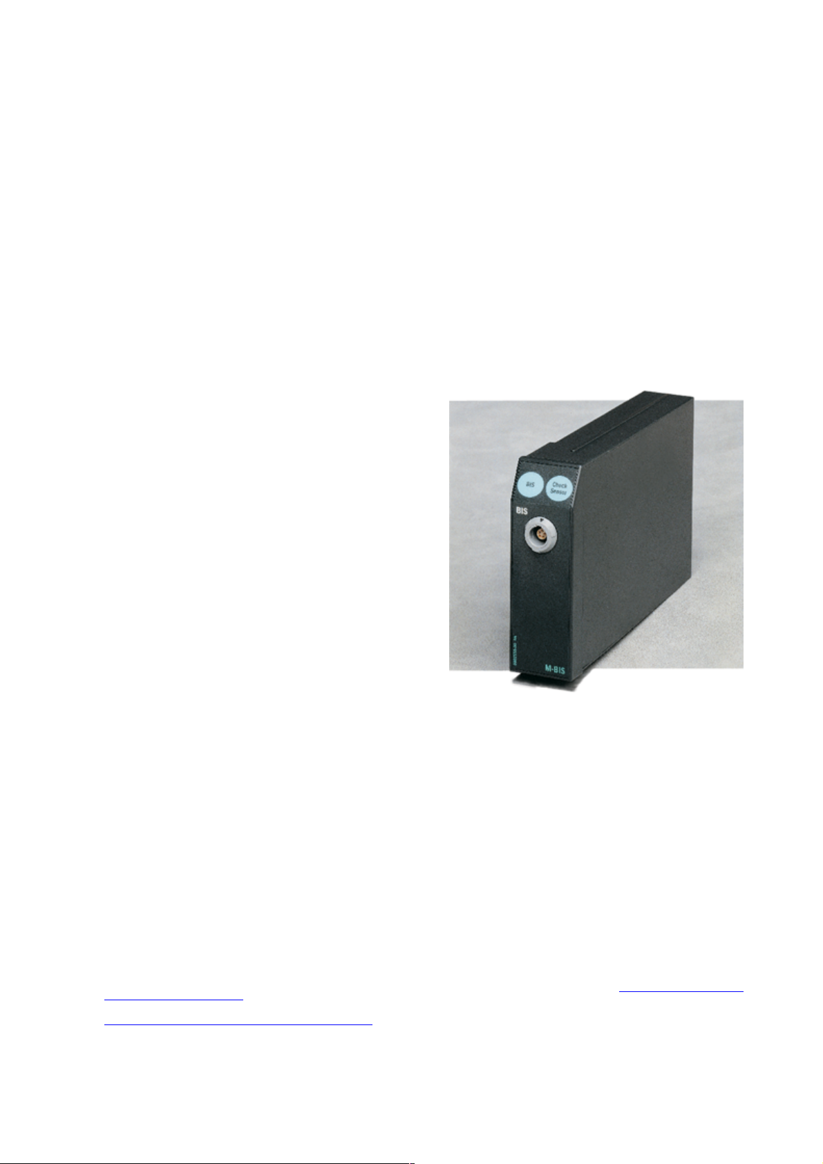
BIS Module, M-BIS
TABLE OF CONTENTS I
TABLE OF FIGURES II
TABLE OF TABLES II
INTRODUCTION 1
1 SPECIFICATIONS 3
1.1 General specifications ..............................................................................................................................3
1.1.1 BIS Module......................................................................................................................................3
1.1.2 Digital Signal Converter, DSC ............................................................................................................3
1.1.3 Environmental specifications ............................................................................................................3
1.2 Technical specifications............................................................................................................................3
2 FUNCTIONAL DESCRIPTION 5
2.1 Measurements principle ...........................................................................................................................5
2.2 Sensor Check ...........................................................................................................................................5
2.3 Main components.....................................................................................................................................7
2.3.1 Digital Signal Converter, DSC ............................................................................................................7
2.3.2 BIS Module......................................................................................................................................8
2.4 Connectors and signals.............................................................................................................................9
2.4.1 Module bus connector......................................................................................................................9
2.4.2 H8 programming connectors pin order...............................................................................................9
2.4.3 BIS Engine connectors pin order......................................................................................................10
2.4.4 Keys ..............................................................................................................................................10
3 SERVICE PROCEDURES 11
3.1 General service information.....................................................................................................................11
3.2 Service check .........................................................................................................................................11
3.2.1 Recommended tools ......................................................................................................................11
3.3 Disassembly and reassembly..................................................................................................................15
4 TROUBLESHOOTING 16
4.1 Troubleshooting chart .............................................................................................................................16
4.2 Messages...............................................................................................................................................17
4.3 Troubleshooting flowchart .......................................................................................................................18
5 SERVICE MENU 19
5.1 BIS service menu....................................................................................................................................20
5.1.1 Module service page ......................................................................................................................20
5.1.2 Sensor...........................................................................................................................................24
5.1.3 Setup.............................................................................................................................................26
6 SPARE PARTS 27
6.1 Spare part list.........................................................................................................................................27
6.1.1 M-BIS ............................................................................................................................................27
7 EARLIER REVISIONS 29
Document No. 800 3476
i
Page 4

Datex-Ohmeda S/5 monitors
APPENDICES A, B 31
SERVICE CHECK FORM A-1
APPENDIX B, HOW TO READ HEX NUMBERS B-1
TABLE OF FIGURES
Figure 1 Measurement setup .............................................................................................................................1
Figure 2 BIS sensor check..................................................................................................................................5
Figure 3 BIS measurement system block diagram............................................................................................... 7
Figure 4 Block diagram of setup.........................................................................................................................8
Figure 5 BIS module disassembly and reassembly............................................................................................15
Figure 6 BIS module troubleshooting flowchart ................................................................................................. 18
Figure 7 Exploded view of module box and BIS module .....................................................................................27
TABLE OF TABLES
Table 1 Module bus connector (X1) pin description............................................................................................ 9
Table 2 Connector pinning for H8 programming connector................................................................................. 9
Table 3 Connector pinning for DSC and BIS Engine connectors........................................................................10
Table 4 Connector pinning BIS Engine power connector ..................................................................................10
Table 5 Connector pinning for BIS Engine serial data connector.......................................................................10
Table 6 Key connector pin assignments...........................................................................................................10
Table 7 Module general status........................................................................................................................21
Table 8 BIS Engine status ..............................................................................................................................21
Table 9 BIS Engine and DSC error messages ...................................................................................................22
Table 10 DSC status....................................................................................................................................25
Table 11 Sensor status................................................................................................................................25
Table 12 BE powup stat...............................................................................................................................25
Table 13 HEX to binary conversion ...............................................................................................................B-1
ii
Document No. 800 3476
Page 5
INTRODUCTION
This Technical Reference Manual Slot provides information for the maintenance and service of the
Datex-Ohmeda S/5 BIS Module, M-BIS. The BIS module is a single width plug-in module designed
for use with the S/5 monitors. Later in this manual modules can be called w/o system name
Datex-Ohmeda S/5.
BIS, and the BIS logo are trademarks of Aspect Medical Systems Inc., and are registered in the
USA, EU and other countries. Later in this manual Aspect Medical Systems Inc. will be called
Aspect.
Please see also the Technical Reference Manual of the S/5 monitor for system specific information
e.g. related documentation, conventions used, symbols on equipment, safety precautions, system
description, system installation, interfacing, functional check and planned maintenance.
The BIS module is indicated for monitoring the state of the brain by data acquisition of EEG signals.
BIS may be used as an aid in monitoring the effects of certain anesthetic agents. The raw EEG
signals are processed to produce a single number, ranging from 100 for a patient being wide
awake to 0 in the absence of brain activity.
Calculated parameters are:
S/5 BIS Module, M-BIS
• Bispectral Index, BIS
• Suppression Ratio, SR
• Electromyograph EMG
• Signal Quality Index, SQI
The calculated parameters can be selected on the display, and trended, (excluding SQI).
Module has two user keys, BIS for BIS menu and Check Sensor for impedance check.
3
1
2
1
4
2
4
3
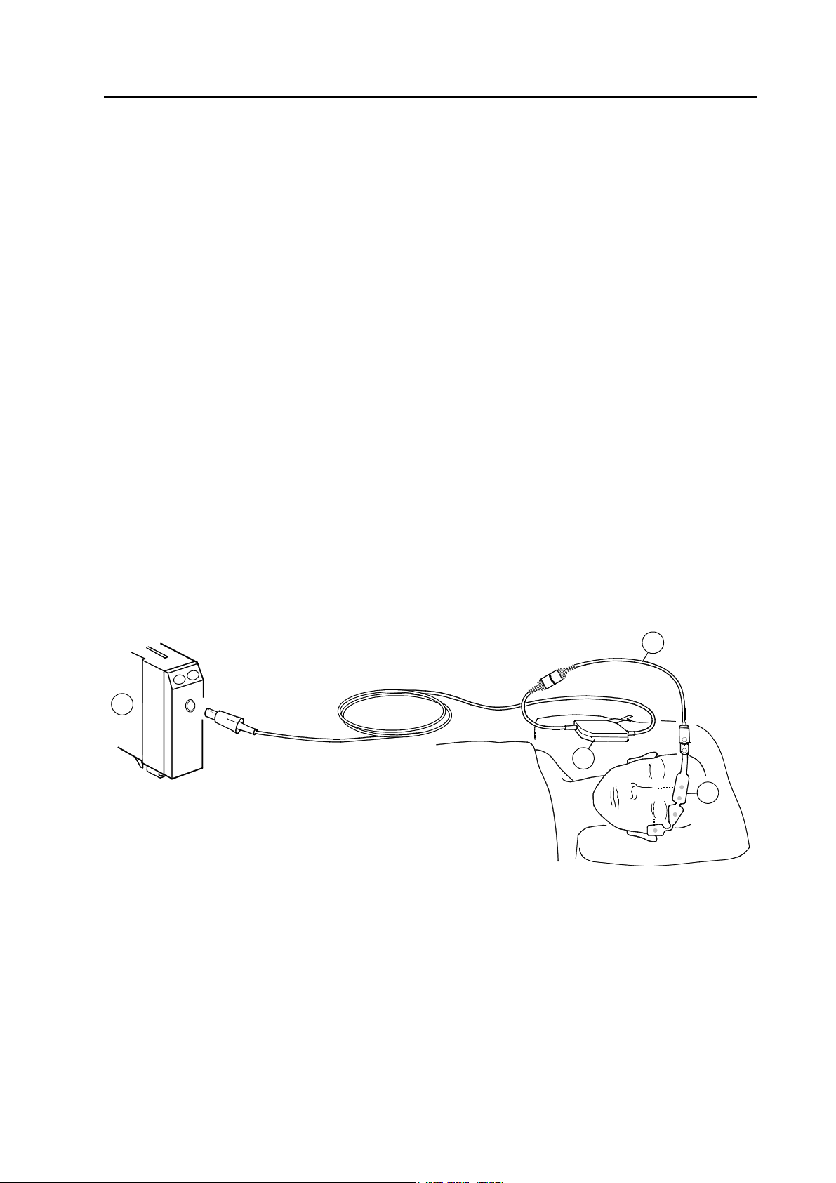
Figure 1 Measurement setup
(1) Module with BIS measurement capability, M-BIS
(2) Digital Signal Converter
(3) Patient Interface Cable
(4) BIS Sensor
NOTE: M-BIS module functions only with monitor software versions 02 or later.
1
Document No. 800 3476
Page 6

Datex-Ohmeda S/5 monitors
Accessories
The BIS measurement is based on Aspect Medical Systems Inc. technology, and all accessories
are developed and manufactured by Aspect.
NOTE: Only Aspect accessories can be used with the M-BIS module.
2
Document No. 800 3476
Page 7

1 SPECIFICATIONS
1.1 General specifications
1.1.1 BIS Module
Module size, W × D × H 37 × 180 × 112 mm/1.5 × 7.1 × 4.4 in
Module weight 0.3 kg/0.7 lbs
Power consumption 2.2 W
1.1.2 Digital Signal Converter, DSC
DSC size, W × D × H 66 × 108 × 25 mm/2.6 × 4.3 × 1.0 in
DSC weight 0.134 kg/0.3 lbs
Integral DSC Cable length 3.6m / 12.5 ft
Patient Interface Cable (PIC Plus)
length 1.2m / 4 ft
S/5 BIS Module, M-BIS
1.1.3 Environmental specifications
Operating temperature +10 … +40°C
storage temperature -25 … +70°C
relative humidity 10 … 95%, non -condensing
atmospheric pressure 700 … 1060 mbar
Protection against electrical shock Type BF
1.2 Technical specifications
Parameter specifications
BIS EEG
Epoch duration 2 seconds
Artifact rejection automatic
EEG scales 25 to 400 µV
EEG sweep speeds 12.5 / 25 / 50 mm /sec
Bispectral index (BIS) 0 to 100
Signal quality index (SQI) 0 to 100
EMG 30 to 80 db (70 to 110 Hz)
Suppression ratio (SR) 0 to 100 %
Update rate 1 second for BIS index
Filters 2 - 70 Hz bandpass (default) / 0.25Hz highpass
Smoothing rate 15 seconds, default in S/5 AM and CAM
30 seconds, default in S/5 CCM and CCCM
3
Document No. 800 3476
Page 8

Datex-Ohmeda S/5 monitors
DSC
Analog to digital converter noise-shaped sigma-delta
Sampling rate 16384 samples/second
Resolution 16 bits at 256 samples/second
Input impedance >50 Mohms
Noise < 0,3µV RMS (2.0µV peak-to-peak) 0.25 to 50 Hz
Common mode rejection 110 dB at 50/60 Hz to earth ground (Isolation mode)
Bandwith 0.16 to 450 Hz
4
Document No. 800 3476
Page 9
2 FUNCTIONAL DESCRIPTION
2.1 Measurements principle
The BIS measurement is based on EEG signals, these are processed as BIS index. The BIS sensor is
placed on the patient’s forehead to acquire the high-resolution signals required. These EEG signals
are transferred to digital signal converter DSC that amplifies and digitizes the EEG signal and sends
it to the module. The module calculates BIS index and sends it to the monitor via MBUS.
BIS measurement on the monitor screen
The waveform field shows the BIS EEG waveform. The following BIS related data appears in digit
fields and graphical trends (except SQI):
BIS number indicates the patient’s level of hypnosis, ranging from 100 for wide awake to 0 in the
absence of brain activity.
Signal Quality Index (SQI ) bar graph indicates the quality of the EEG signal in the range of 0 to
100.
S/5 BIS Module, M-BIS
Electromyograph (EMG) bar graph represents the absolute power in the 70 to 110 Hz frequency
band and ranges from 30 to 55 dB. This frequency band contains power from muscle activity
(electromyograph) as well as power from high frequency artifacts.
Suppression ratio (SR) number indicates the percentage of suppressed (flatline) EEG detected
over the last 63 seconds. It ranges from 0 to 100%.
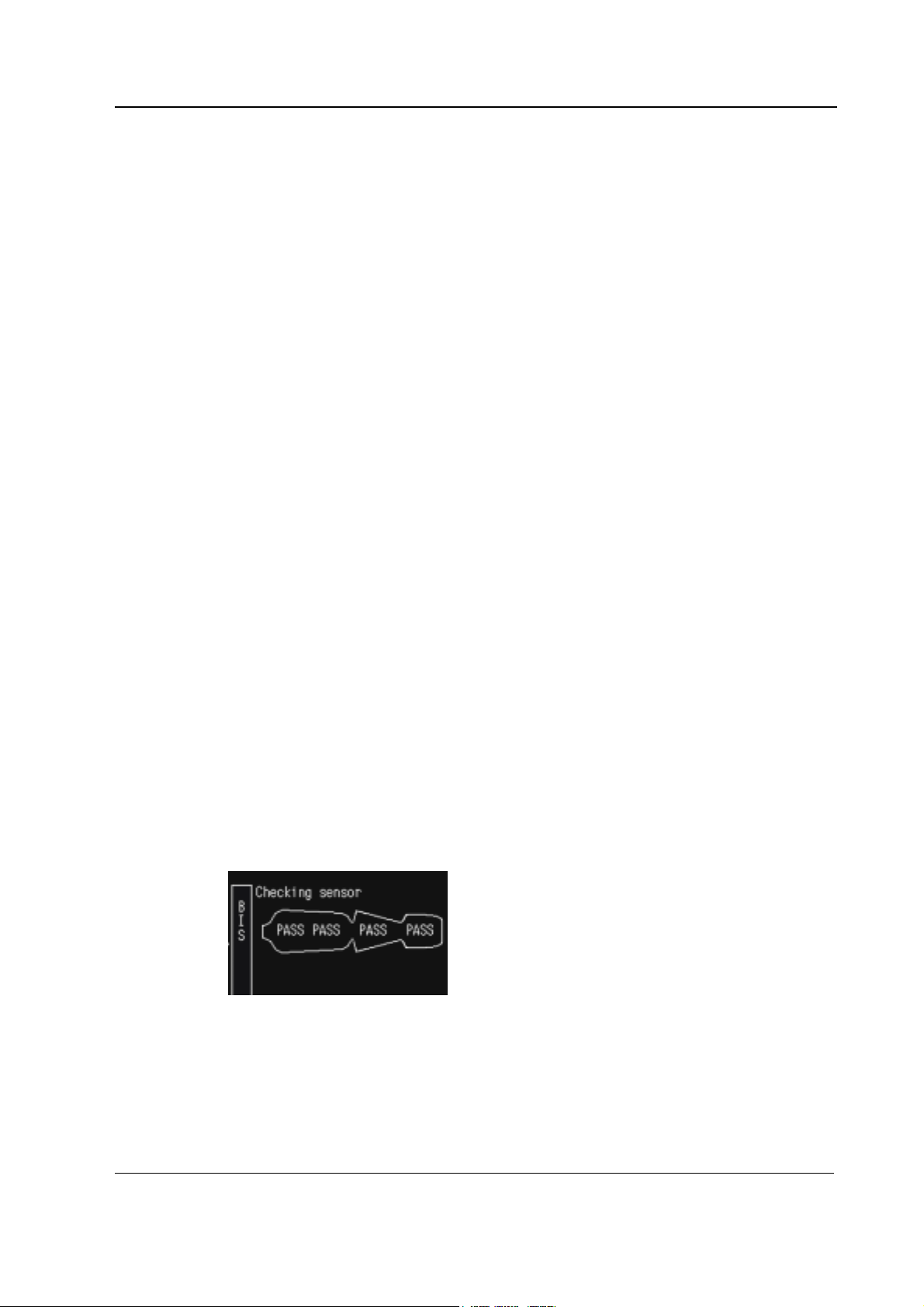
2.2 Sensor Check
Sensor check is performed automatically at the beginning of each case when the sensor is
attached to the patient interface cable (monitor). An initial check-up message is shown at digit
field together with an appropriate sensor picture. The information of the passed or failed sensor
check is printed to this picture at each electrode’s location. The BIS measurement can’t continue if
the first sensor check fails. In such case a message “Sensor check failed” is shown at the digit and
waveform field.
Figure 2 BIS sensor check
Continuous checking of the reference and signal electrodes and periodic checking of the ground
electrode is performed by default. It can be switched off by selecting appropriate comand from
menu – message “Automatic check off” will appear. Sensor check can be started manually by
pushing a module key or selecting appropriate command from menu. Manual sensor check can be
useful e.g. when AEP's are being monitored at the same time, as the continuous sensor check
Document No. 800 3476
5
Page 10

Datex-Ohmeda S/5 monitors
might disturb the AEP measurement.
During periodic ground checks, the signal disappears momentarily and the message “Checking
sensor” is printed in the digit and waveform fields. Also, all BIS calculation stops during this check,
and no measurement values are shown.
CAUTION Continuous impedance check may need to be disabled if the 1 nA 128 Hz
impedance check signal interferes with other equipment such as evoked potential.
WARNING Make sure that the electrodes, sensor and connectors do not touch any
electrically conductive material, including earth.
6
Document No. 800 3476
Page 11
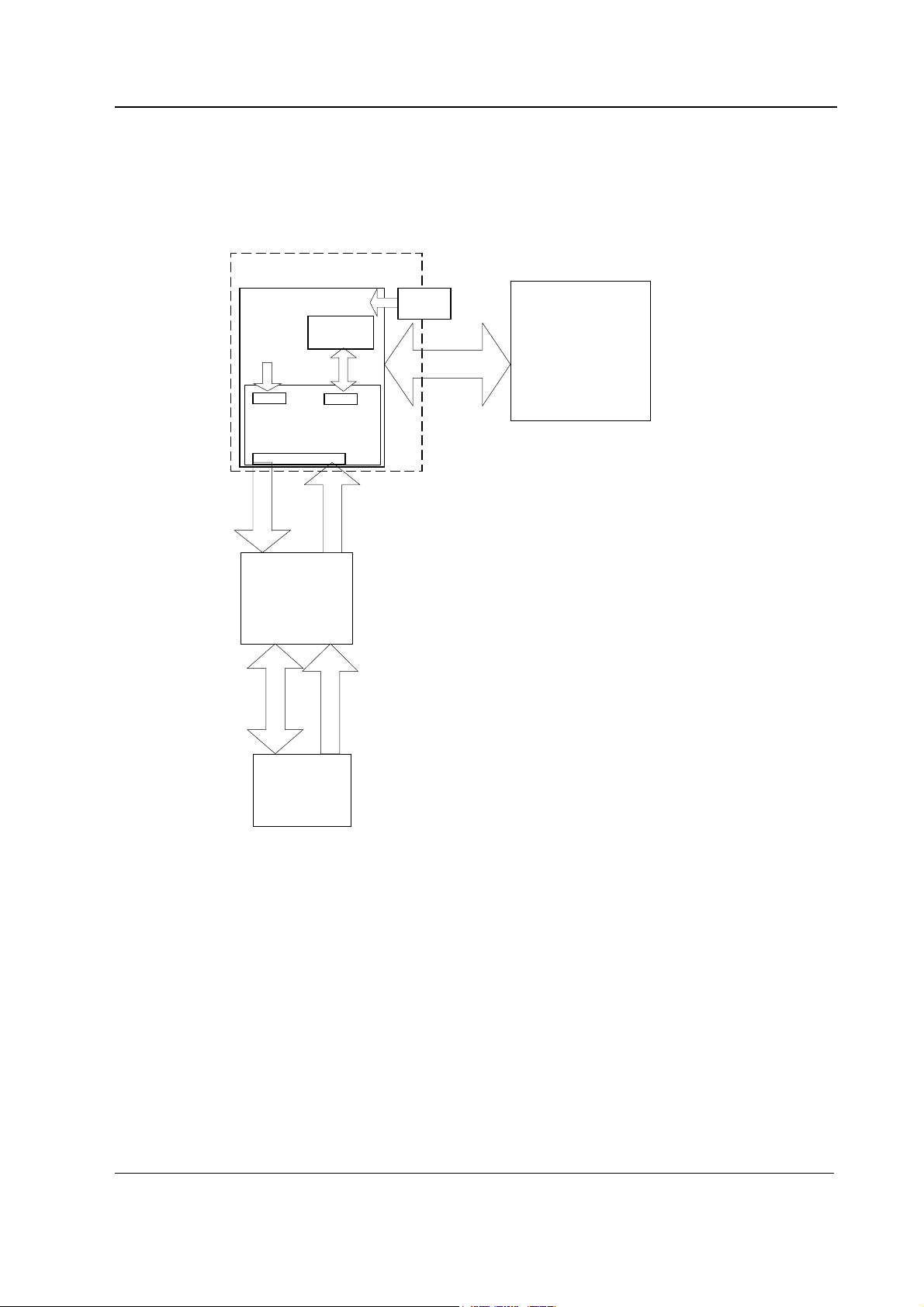
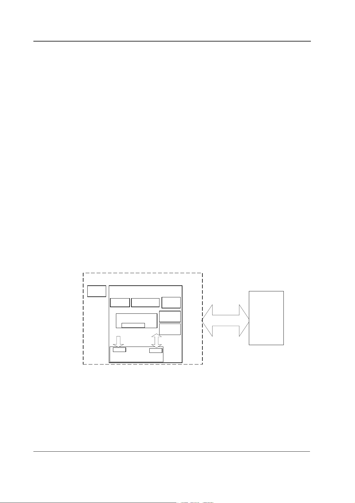
2.3 Main components
BIS measurement chain is composed of Aspect BIS Sensor, Aspect digital signal converter, M-BIS
module containing Aspect BIS Engine board and Datex-Ohmeda’s interfacing board, and host
monitor. Block diagram of the system below.
M-BIS Module
S/5 BIS Module, M-BIS
BIS Interfac ing Boar d
Controller
DSC
data
Serial
Digital signal
Measurement
Power
BIS Engine
Power
Digital Signal
Converter
Patient Isolation
Control
PIC+
Keys
MBUS
Serial
data
Power
Host Monitor
BIS Sensor
Figure 3 BIS measurement system block diagram
2.3.1 Digital Signal Converter, DSC
The digital signal converter, DSC, receives, amplifies and digitizes patient EEG signals. It is placed
close to the patient's head where the EEG signal is less subject to interference from other medical
equipment. The digital signal converter is connected to the module with a 3.6m long shielded
cable and to the BIS sensor with 1.2m long patient interface cable, see Figure 1. For BIS Sensor
related documentation refer to BIS documentation by Aspect, Inc.
CAUTION Do not autoclave the DSC. Do not open it for any reason.
MBIS_meas_blockdiag.vs d
7
Document No. 800 3476
Page 12
Datex-Ohmeda S/5 monitors
WARNING When using the electrosurgery unit, ensure proper contact of the ESU return
electrode to the patient to avoid burns at monitor measurement sites. Also
ensure that the ESU return electrode is near the operating area.
WARNING Radiated field strengths above 1V/m may cause erroneous measurements at
various frequencies. Do not use electrical radiating equipment close to the
DSC.
2.3.2 BIS Module
Aspect BIS Engine
The BIS Module provides Bispectral index values to monitor. The BIS Engine processes the digital
signal from DSC and outputs the BIS index and other supporting parameters through the
asynchronous serial connection. The BIS Engine outputs the BIS Index, raw EEG, EMG, Signal
Quality Index (SQI), Suppression Ratio (SR) and electrode impedance’s. The BIS Engine software
includes Aspects' proprietary algorithm for BIS calculation.
BIS interfacing board
The BIS interfacing board supplies the data from BIS Engine to the monitor via module bus. As well
the module accepts commands from the monitor via module bus. In addition, the module provides
supply voltages and all the required control signals to the BIS Engine and DSC.
Controller H8 has on-chip RAM and FLASH ROM, external SRAM and EEPROM.
Figure 4 Block diagram of setup
Keys
M-BIS Module
BIS Interfacing Board
SRAM EEPROM
H8 Controller
FLASH
Power
Aspect BIS Engine
data
Serial
Prog
RS485
RESET
MBUS
Serial
data,
Power
Host Monitor
BIS Interface board Block.vsd
8
Document No. 800 3476
Page 13

2.4 Connectors and signals
2.4.1 Module bus connector
S/5 BIS Module, M-BIS
13
25
1
14
Table 1 Module bus connector (X1) pin description
PIN Name Description
1 Reset_ RS485 Module Bus Reset +
8 Nreset_ RS485 Module Bus Reset -
6 Data_ RS485 Module Bus Data +
5 Ndata_ RS485 Module Bus Data -
3 +15VD +15V Supply voltage
7 GND Ground
13 GND Ground
15 GND Ground
22 RS232_TXD BIS-Engine SW update, data out,
no monitor use
23 RS232_RXD BIS-Engine SW update, data in,
no monitor use
24 +5,1V +5V Supply voltage
25 +5,1V +5V Supply voltage
Other NC Not Connected
2.4.2 H8 programming connectors pin order
10
9
Table 2 Connector pinning for H8 programming connector
PIN Name Description
1 GND Ground
2 PRG_FB Program feedback
3 TxD Data output to programmer
4 RxD Data input from programmer
5 /RESET RESET input from programmer
6 VDD Power input from programmer
7 PRG_VCC Programming voltage from programmer
8 MODE.2/BOOT Control input from programmer
9 PCFB Programmer Connector feedback / GND
10 CODE_RES Coding resistor output to programmer
2
1
Document No. 800 3476
9
Page 14

Datex-Ohmeda S/5 monitors
2.4.3 BIS Engine connectors pin order
Table 3 Connector pinning for DSC and BIS Engine connectors
PIN
Redel
1 DSC_OUTA 2 Power out A
2 DSC_OUTB 4 Power out B
3 DSC_IN 6 Data input
4 DGND 7,8,9,10 Ground
5 Chassis Ground 1,3,5, Ground
Name PIN
Samtec
Description
Table 4 Connector pinning BIS Engine power connector
PIN Name Description
1, 2 +12V +12V Power output for BE
5,6,7,8 +5V +5V Power output for BE
3,4,9,10 GND Ground
Table 5 Connector pinning for BIS Engine serial data connector
PIN Name Description
1 RS232_RXD Data input to BE
2 TTL_RXD Data input to BE
3 RS232_TXD Data output from BE
4 TTL_TXD Data output from BE
5 NC Not Connected
6 NC Not Connected
7 RS232_RESET Reset input to BE
8 /TTL_RESET /RESET input to BE
9 GND Ground
10 /USE_TTL TTL/RS232 selection input to BE
2.4.4 Keys
10
Document No. 800 3476
Table 6 Key connector pin assignments
PIN Name Description
1 GND Ground /NC
2 Key 1 Key 1, right
3 Key 2 Key 2 left
4 GND Ground
5 GND Ground / Shield
5
1
Page 15

S/5 BIS Module, M-BIS
3 SERVICE PROCEDURES
3.1 General service information
Field service of the M-BIS is limited to replacing faulty circuit boards or mechanical parts. Faulty
circuit boards should be returned to Datex-Ohmeda for repair.
Datex-Ohmeda is always available for service advice. Please provide the unit serial number, full
type designation, and a detailed description of the fault.
The Datex-Ohmeda BIS Simulator (order No. 900509) is recommended for functional checks.
CAUTION Only trained personnel with appropriate equipment should perform the tests and
repairs outlined in this section. Unauthorized service may void warranty of the unit.
3.2 Service check
These instructions include complete procedures for a service check. The service check should be
performed after any service repair. However, the service check procedures can also be used for
determining possible failures.
The procedures should be performed in ascending order.
The instructions include a check form, Service check form, which should be filled in when
performing the procedures.
The mark
the procedure.
The procedures are designed for monitors with S/5 monitor software of revision 02.
? in the instructions means that the check form should be signed after performing
3.2.1 Recommended tools
Tool Order No. Notes
BIS Simulator or
BIS Sensor simulator
Screwdriver
900509
900508
11
Document No. 800 3476
Page 16

Datex-Ohmeda S/5 monitors
• Detach the module box by removing the two screws from the back of the module. Be careful
with the loose latch and spring pin for locking.
1. Check internal parts:
− screws are tightened properly
− cables are connected properly
− there are no loose objects inside the module
?
2. Check external parts of the module:
− the front cover and the front panel sticker are intact
− connectors are intact and are attached properly
− the module box, latch and spring pin for locking are intact
Reattach the module box
?
3. Check the external parts of the Digital Signal Converter
− - the cover and the panel stickers are intact
− - cables and their connections are intact
Do not connect DSC to the module yet
?
Turn the monitor on and wait until the normal monitoring screen appears.
• Configure the monitor screen so that information regarding the BIS measurement is shown:
Monitor Setup - Screen 1 Setup – Waveform Fields – Field1 – BIS EEG
Others – BIS – Scale - 100uV
Others – BIS – Smoothing Rate 15s
4. Installation
Plug in the module. Check that it goes in smoothly and engages properly
?
12
Document No. 800 3476
5. Recognition of module
Check that the module is recognized, i.e. the BIS header with related information appears in
the chosen waveform field and ‘Cable off’ message is shown on field.
?
Page 17

S/5 BIS Module, M-BIS
6. Enter the service menu:
Monitor Setup - Install/Service (password 16-4-34) - Service (password 26-23-8)
Record the information regarding the module software of M-BIS by selecting SCROLL VERS
and turning the ComWheel.
Note! DSC related data will appear only when the DSC is connected for the first time after
start-up.
?
7. Recognition of DSC
Connect the PIC+ cable to the DSC.
Connect the DSC to the module.
- Check that the DSC is recognized (DSC related data appears to the page)
- Check that ‘No sensor’ appears to the selected waveform field.
?
8. Enter the BIS module service menu:
Parameters - More… - BIS
Check that the ‘Mod Mon Timeouts’, ‘ Mon Mod Bad checksums’ , ‘ Mod Mon Bad
Checksums’, ‘ Bad Checksums from BIS’ values in the module view are not increasing faster
than by 5 per second. Check that the memories of the module have passed the internal
memory test, i.e. ‘RAM’, ‘ROM’ and ‘EEPROM’ all state OK.
?
9. Check the BIS and Sensor Check membrane keys of the module. Stay in the module view
and press each key for at least one second and check that the key being pressed is identified,
i.e. the corresponding PRESSED text appears in the service menu.
?
10. Check that ‘ Messages from BE ’ are increasing steadily.
?
13
Document No. 800 3476
Page 18

Datex-Ohmeda S/5 monitors
11. Go to the Sensor page.
Check that
- no sensor is identified
- mains frequency is set correctly
- check that ‘ BE powerup test’, ‘DSC selftest Ch1’ and ‘DSC selftest Ch2’ all show PASs
(if not, go to BIS Setup page, perform DSC Test and check the results again)
?
12. Sensor check
Connect the BIS simulator to the PIC+ cable. See that ‘Checking sensor’ text and image
appear. Wait for a while seconds and check that all sensors show PASS. Check that the
‘Sensor type’ shows Demo Sensor.
?
13. Check that the ‘BIS’, ‘SQI’ and ‘SR’ values are between 0..1000, and the ‘EMG’ value
between 0..10000. Note! If Sensor simulator 900508 is used, the values can be out of the
given range.
?
14. Go to the Module page
Check that no BIS Engine errors appear.
?
15. Perform sensor check by pressing ‘Check Sensor’ and verify sensor passes.
?
16. Perform an electrical safety check and a leakage current test.
?
17. Check that the module functions normally after performing the electrical safety check.
?
14
Document No. 800 3476
18. Clean the module with suitable detergent.
?
• Fill in all necessary documents.
Page 19

3.3 Disassembly and reassembly
S/5 BIS Module, M-BIS
Figure 5 BIS module disassembly and reassembly
Disassemble the M-BIS in the following way.
1. Remove the two screws from the back of the module.
2. Pull the module box slowly rearward and detach it from main body. Be careful with the loose
latch and spring locking pin.
3. Detach the BIS Engine board by removing the four screws located at the corners of the board
and disconnecting the front panel connector cable.
4. Detach the interface board by removing the two screws located near the front panel frame,
disconnect the cable and pull out the front panel frame.
To reassemble the module, reverse the order of the disassembly steps.
CAUTION When reassembling the module, make sure that the cables are reconnected
properly.
15
Document No. 800 3476
Page 20

Datex-Ohmeda S/5 monitors
4 TROUBLESHOOTING
4.1 Troubleshooting chart
Trouble Cause Treatment
No BIS waveforms on screen. BIS waveforms not selected on screen. Press Monitor Setup key and select BIS
waveforms on the screen.
Sensor impedance check is not available on
menus.
Sensor impedance check fails Sensor poorly attached Attach the sensor by following the sensor
Sensor is not connected to the DSC or DSC
is not connected to the module
Connect the sensor and the DSC
instructions
16
Document No. 800 3476
Page 21

S/5 BIS Module, M-BIS
4.2 Messages
The messages below will appear in the BIS digit field (DF), BIS waveform field (WF) or at the message field (MF) at
the upper section of the Datex-Ohmeda S/5 patient monitor display.
Message Location Cause Treatment
Cable off
BIS cable off
No Sensor
No BIS Sensor
Incompatible sensor DF Sensor is not recognized.
Incompatible DSC DF Current module hw/sw is incompatible
Sensor check failed
BIS sensor
check failed
Poor signal DF Artifacts, or the amount of EMG activity
Checking sensor DF Sensor check in progress. Can be either
Checking Sensor –
message stays more
than 2 min.
Automatic check off DF Continuous sensor checking has been
Replace Sensor DF The sensor has passed its use by date
High BIS impedance DF Sensor is not attached properly to the
Artifact DF Non-EEG data such as EMG, eyeblinks or
Module error DF BIS Engine failure
DSC Error DF
Demo data MF BIS simulator is connected Disconnect the BIS simulator
DF
MF
DF
MF
DF
MF
DF Sensor check fails, the sensor is not
MF
DSC cable is not connected to the module. Connect the DSC to the module
Sensor is not connected to PIC+ cable or
PIC+ cable is not connected to the DSC
Sensor is not a BIS sensor.
with this DSC
E.g. DSC-2
Sensor check failed, one or more of the
electrode impedances exceeds the
threshold.
prevents calculating BIS, data excluded.
SQI < 50
the initial sensor check, manual check or
the periodic check.
attached to the patient while connected to
the PIC+ cable
turned off
The sensor has been used for 24h
patient
shivering present.
for more information see service page
description
The DSC is not communicating or
operating properly. This may occur during
the use of electrocautery device.
For more information see service page
description
Connect the Sensor to the PIC+ cable
Connect the PIC+ cable to the DSC
Replace sensor and then PIC+ cable.
Connect correct type of sensor
Make sure PIC connector is clean and dry
Connect correct type of DSC
Reattach the sensor to the patient by
following the sensor instructions
Replace the sensor
Check PIC+ cable and then DSC
Check the sensor then the PIC cable.
Reattach the sensor to the patient by
following the sensor instructions
Wait until the check has been performed
Attach the sensor to the patient and press
the Check Sensor button on the module
front panel
Turn the check on from the BIS menu
Replace with a new sensor
Check the cable connections
Reattach the sensor to the patient by
following the sensor instructions
Wait for good data
Replace the BIS Engine
Replace the DSC
If the message persists, the BIS Engine
may require service.
17
Document No. 800 3476
Page 22

Datex-Ohmeda S/5 monitors
4.3 Troubleshooting flowchart
Probably faulty
BIS Module
Take all modules
out of the frame.
Enter the Service
menu ID page
Is the module
ID displayed?
K
?
O
Yes
Enter the BIS
Service menu
Check are the Mod Mon Timeouts,
Mod Mon Bad checksums,
Mon Mod Bad Checksums or
Bad checksums from BE running?
?
O
K
Yes
Check RAM, ROM
and EEPROM
Insert M-BIS and turn power on
(keep DSC disconnected)
Y
s
e
Fault not in BIS
No
Y
s
e
m
a
f
a
module
a
u
d
o
h
t
s
e
D
o
l
l
i
t
t
s
l
u
?
r
a
e
p
p
No
No
s
e
D
o
r
e
h
t
o
n
n
i
k
r
w
o
e
l
e
m
a
s
e
?
t
o
l
s
Yes
O
K
?
Yes
Connect DSC into
module connector
D
C
S
s
I
t
s
e
t
f
l
e
s
d
e
s
s
a
p
Check BIS Engine
errors
O
K
?
Check front panel
key functions
O
K
?
Yes
Fault not in BIS
module
Yes
Replace
interface board
N
o
N
o
Replace the DSC
Replace the BIS Engine or DSC
(depending on the error message)
s
e
D
e
h
t
s
o
N
I
y
a
e
p
k
c
e
n
n
o
c
No
Y
s
d
e
t
e
?
d
Connect the
keypad
o
s
a
p
t
s
e
t
e
h
t
e
h
t
o
n
a
h
t
i
w
?
d
a
p
k
y
e
No
Replace BIS
interface board
e
s
Y
s
r
Replace the
keypad
BIS_trbl.vsd
18
Document No. 800 3476
Figure 6 BIS module troubleshooting flowchart
Page 23

5 SERVICE MENU
S/5 BIS Module, M-BIS
Press the Monitor Setup key - select Install/Service (password: 16-4-34) - select Service
(password: 26-23-8) - select Parameters - More... - BIS.
19
Document No. 800 3476
Page 24

Datex-Ohmeda S/5 monitors
5.1 BIS service menu
5.1.1 Module service page
Check Sensor activates the sensor impedance check.
Module
Measurement indicates if BIS Engine is on: ON/OFF
Imp.Check Key indicates that the key in the module front panel works properly.
Bis Menu Key indicates that the key in the module front panel works properly.
Impedance Meas indicates the impedance measurement mode. The modes are
CYCLIC/COMBINED/GROUND/OFF
BIS Engine errors: error messages created by DSC or BIS Engine. See "Table 9" below for
detailed description of the error message
Statuses (HEX): See appendix B; How to read HEX numbers.
General Status1 indicates the general status of the module. See "Table 7" to see the detailed
description of the message
Bis_status1 indicates the BIS Engine status. See "Table 8" to see the detailed description of the
message
Msgs to BE number of data packages sent from interface board to BIS Engine
Msgs from BE number of data packages sent from BIS Engine to interface board
Mod Mon Timeouts is a cumulative number that indicates how many times the module (interface
board) has not responded to monitor’s inquiry.
Mod Mon Bad Checksum is a cumulative number that indicates how many times there has been
an error in the message from module (interface board) to monitor.
Mon Mod Bad Checksum is a cumulative number that indicates how many times there has been
an error in the message from monitor to module (interface board).
Bad Checksums from BIS is a cumulative number that indicates how many times there has been
an error in the message from the BIS Engine to module interface board.
20
Document No. 800 3476
Page 25

RAM indicates the state of the RAM memory.
ROM indicates whether the checksum at the EPROM is accordance with the one the software has
calculated.
EEPROM indicates if the values stored in permanent memory are valid.
The states in memory checks are OK, Fail or ? (module not in place or a communication error).
Measured parameters indicated:
BIS indicates BIS index ; range 0..1000 (corresponds 0..100)
SQI indicates signal quality index; range 0..1000 (corresponds 0..100)
EMG indicates EMG activity level; range 0..10000 (corresponds 0..100dB NOTE! On the display
EMG will be shown between 30..55dB on the bar graph or 30..80dB on the trend)
SR indicates supression ratio; range 0...100 (corresponds 0..100%)
General_Status1 Module general status.
Table 7 Module general status
bit 0-5 Not used
bit 6 State error
bit 7 Communication failure
bit 8 Power failure
bit 9 Clock failure
bit 10 EEPROM checksum failure
bit 11 EEPROM writing failure
bit 12 ROM failure
bit 13 RAM failure
bit 14 Test mode
bit 15 Init mode
S/5 BIS Module, M-BIS
BIS_Status1 BIS Engine status
Table 8 BIS Engine status
bit 0 Check Sensor key pressed
bit 1 BIS key pressed
bit 2 Inpedance check mode cyclic
bit 3 Impedance check mode combined
bit 4 Impedance check mode ground
bit 5 Impedance check off
bit 6 Measurement on
bit 7 EEG measurement on
bit 8 Impedance check on DSC channel 1 passed
bit 9 Impedance check on DSC channel 2 passed
bit 10 BIS Engine powerup failure
bit 11 DSC selftest failure
bit 12 DSC quick test failure
bit 13 DSC selftest on
bit 14 No data from BIS Engine
bit 15 Not used
21
Document No. 800 3476
Page 26

Datex-Ohmeda S/5 monitors
Table 9 BIS Engine and DSC error messages
Message Errors of type 1
DSC buffer overrun
Out of dynamic memory
Execution time exceeded in main
Error in algorithm processing
Invalid state in UART receive state machine UART related errors
UART initalization error
Transmit queue full
Illegal number of data bytes for packet to be transmitted
to the Host
Illegal number of channels for EEG data Misc. errors
Illegal EEG data type
Illegal EEG data rate
Illegal EEG filter coefficients
No updates from Host Communication related errors
Bad CRC - TI_SELFTEST_CODE EEPROM CRC checks
Bad CRC - TI_RUN_CODE
Bad CRC - FPGA_CONFIG
Bad CRC - REV_INFO
Illegal serial number Serial number check
DSC failed to power up DSC related errors
Serious DSC overcurrent error
DSC receiver data overrun
DSC failed repeatedly in responding to commands
DSC update failed
Serious DSC power regulation fault
General DSC failure
Sensor Negative Ground Fault Smart sensor errors
Serious Sensor Positive Ground Fault
Serious Sensor Overcurrent Fault
22
Document No. 800 3476
Page 27

Message Errors of type 2
Illegal message ID Errors for layer 3 packets
Illegal command parameter
Illegal length for layer 2 data
Disabled interrupt received UART transmitter empty interrupt
Disabled interrupt received UART modem interrupt
No status nibble received DSC related errors
DSC not connected
DSC disconnected after test failure
Illegal DSC ID
DSC power regulation fault
DSC interface fault
DSC did not respond to command
Illegal PIC ID
DSC overcurrent
DSC overrun
EEPROM Bad packet length Software update related errors
EEPROM Bad checksum
EEPROM Bad code length
EEPROM Illegal packet subtype
EEPROM physical write error
EEPROM NOT_DATA_TIMEOUT
UART related errors
S/5 BIS Module, M-BIS
23
Document No. 800 3476
Page 28

Datex-Ohmeda S/5 monitors
5.1.2 Sensor
Sensor type: indicates the type of the sensor connected
Lot code: indicates the manufacturing lot code of the sensor. The lot code contains the
manufacturing date and shift
Serial no: indicates the serial number of the sensor.
Shelf life: indicates max storage duration
Usage count: indicates how many times the sensor has been attached/detached. Not Active!!
Mains Freq.: indicates the set mains frequency; 50Hz/60 Hz
Sensor Impedances: indicates the last measured impedances
Imped. indicates the measured impedance value in Kohms.
Qualif. indicates the quality of the measured impedance; PASS/FAIL
BE powerup test: indicates the status of BIS Engine power up test: PASS/FAIL
DSC selftest ch1: indicates the DSC selftest status for channel 1: PASS/FAIL
DSC selftest ch2: indicates the DSC selftest status for channel 2: PASS/FAIL
Measured parameters indicated:
BIS indicates BIS index ; range 0..1000 (corresponds 0..100)
SQI indicates signal quality index; range 0..1000 (corresponds 0..100)
EMG indicates EMG activity level; range 0..10000 (corresponds 0..100dB
(NOTE! On the trend display EMG will be shown between 30..80dB)
SR indicates supression ratio; range 0...100 (corresponds 0..100%)
Statuses (HEX): See "APPENDIX B"How to read HEX numbers.
DSC status: indicates the DSC status for the four channels. See "Table 10" to see the detailed
description of the message.
Sensor status: indicates the Sensor status. See "Table 11" to see the detailed description of the
message.
BE powup stat: indicates the BE power up status. See "Table 12" to see the detailed description
of the message.
24
Document No. 800 3476
Page 29

Table 10 DSC status
bit 0 Noise test
bit 1 BIS key pressed
bit 2 Blocked droop test
bit 3 Unblocked gain test
bit 4 Impedance wait time out test
bit 5 Noise timeout test
bit 6 Blocked timeout test
bit 7 Unblocked timeout test
bit 8 DSC not connected test
bit 9 Not used test
bit 10 Not used test
bits 11 - 15 Not used
Table 11 Sensor status
bit 0 Quick selftest pass
bit 1 Quick selftest gain
bit 2 Quick selftest noise
bit 3 Quick selftest fail
bit 4 Quick selftest valid
bit 5 Sensor valid
bit 6 Sensor invalid
bit 7 Sensor too many uses
bit 8 Sensor expired
bit 9 Sensor validity unknown
bits 10 -15 Not used
S/5 BIS Module, M-BIS
Table 12 BE powup stat
bit 0 XRAM test
bit 1 Dma test
bit 2 Timer test
bit 3 Fpga test
bits 4 -15 Not used
25
Document No. 800 3476
Page 30

Datex-Ohmeda S/5 monitors
5.1.3 Setup
Automatic Check: A selection to define whether automatic sensor check is used ON/OFF
Test DSC indicates the status of the DSC self test; PASS/FAIL
Filters: A selection to define if filters are used
ON; disturbances are filtered from the raw EEG signal
OFF; raw EEG signal is shown
26
Document No. 800 3476
Page 31

6 SPARE PARTS
6.1 Spare part list
6.1.1 M-BIS
S/5 BIS Module, M-BIS
Figure 7 Exploded view of module box and BIS module
Item Description Order code
1 Module box (single width) 886167
2 Latch 879181
3 Spring pin 879182
4 Cross recess screw, M3×8 black 616215
5 Front panel unit 8002476
6 Membrane keypad 880101
7 Cross cylinder head screw, M3×12 628700
8 Metal frame 879184
9 Cross cylinder head screw, M3×6 61721
10 BIS interface board 8002285
11 Aspect BIS engine board 900505
12 BIS connector unit, M-BIS 8002480
27
Document No. 800 3476
Page 32

Datex-Ohmeda S/5 monitors
Item Description Order code
13 Front panel sticker, M-BIS, DA 8002855
13 Front panel sticker, M-BIS, DE 8002848
13 Front panel sticker, M-BIS, EN 8002555
13 Front panel sticker, M-BIS, ES 8002853
13 Front panel sticker, M-BIS, FI 8002847
13 Front panel sticker, M-BIS, FR 8002852
13 Front panel sticker, M-BIS, IT 8002850
13 Front panel sticker, M-BIS, JA 8003001
13 Front panel sticker, M-BIS, NO 8002849
13 Front panel sticker, M-BIS, NL 8002856
13 Front panel sticker, M-BIS, PT 8002854
13 Front panel sticker, M-BIS, SV 8002851
28
Document No. 800 3476
Page 33

7 EARLIER REVISIONS
Revision Manual slot/main manual Note
No previous revisions
S/5 BIS Module, M-BIS
29
Document No. 800 3476
Page 34

Datex-Ohmeda S/5 monitors
30
Document No. 800 3476
Page 35

APPENDIX A, Service check form, S/5 BIS Module, M-BIS
APPENDICES A, B
31
Document No. 800 3476
Page 36

Datex-Ohmeda S/5 monitors
This page intentionally left blank.
32
Document No. 800 3476
Page 37

SERVICE CHECK FORM
BIS Module, M-BIS
Customer
APPENDIX A, Service check form, S/5 BIS Module, M-BIS
Service
Service engineer Date
OK = Test OK N.A. = Test not applicable Fail = Test Failed
Service check
OK N.A. Fail OK N.A. Fail
1. Check internal parts: 2. Check external parts of
3. Check the external
parts of DSC
5. Recognition of module
6. module software
7. Recognition of DSC 8. Communication and
9. membrane keys 10. Messages from BE
M-BIS
Module type S/N
the module:
4. Installation
memories of module
11. Sensor IDSensor 12. Sensor check
13. Checks with simulator Allowed range
BIS 0…1000
SQI 0…1000
SR 0…100
EMG 0…10000
14. BIS Engine errors 15. check
A-1(2)
Document No. 800 3476
Page 38

Datex-Ohmeda S/5 monitors
OK N.A. Fail OK N.A. Fail
16. Electrical safety check 17. Functioning after
electrical safety check
18. Final cleaning
Notes
Used Spare Parts
Signature
A-2(2)
Document No. 800 3476
Page 39

APPENDIX B, How to read hex numbers, S/5 BIS Module, M-BIS
APPENDIX B, HOW TO READ HEX NUMBERS
Some statuses on BIS Module service pages are given as HEX (hexadecimal) numbers. To
understand them, please read the following:
A HEX number has a base of 16 instead of 10. This means that every character in a number can
have a value between 0 and 15. Numbers from 0 to 9 are displayed as if they were normal 10based numbers. Numbers from 10 to 15 are displayed with letters from a to f or A to F respectively.
Every character of a HEX number expands into a binary code of four 0:s (zeroes) and 1:s (ones) as
given in table 13. Four successive characters thus expand into four times four binary numbers.
Here's an example:
We have a HEX number F3A1. We expand the number into binary code so that we first take the four
binary digits that correspond to F, which are 1111. Then we write the four binaries that correspond
to 3 (0011) after the first four. We now have 11110011. And so on.
Eventually, we have a string of 16 binary numbers, so called bits. HEX number F3A1 corresponds to
a binary code of 1111 0011 1010 0001. Spaces are added here for legibility and to visualize the
fact that every group of four bits corresponds to one HEX character.
The bits in a binary number are numbered from right to left always starting from 0 as follows:
bit 15
bit 14
bit 13
bit 12
bit 11
bit 10
bit 8
bit 7
bit 6
bit 5
bit 4
bit 3
bit 2
bit 1
bit 0
bit 9
1111 0011 1010 0001
With this information and a table of status fields from section 5 “Service Menu” we can translate a
HEX status code into actual status messages. If a bit is 1 this means that the corresponding
status/error condition is valid, whereas a 0 means that it is not.
Table 13 HEX to binary conversion
HEX binary HEX binary
0 0000 8 1000
1 0001 9 1001
2 0010 A 1010
3 0011 B 1011
4 0100 C 1100
5 0101 D 1101
6 0110 E 1110
7 0111 F 1111
B-1(2)
Document No. 800 3476
Page 40

Datex-Ohmeda S/5 monitors
B-2(2)
Document No. 800 3476
 Loading...