

80CH SEGMENT DRIVER FOR DOT MATRIX LCD
S6B2104
INTRODUCTION
The S6B2104 is a LCD driver IC, which is fabricated by low power CMOS high voltage process technology. This
device consists of 80-bit bi-directional shift register, 80-bit data latch and 80 bit driver.
FEATURES
• Power supply voltage: +5V ± 10%, +3V ± 10%
• Supply voltage for display: 6 to 28V (VDD-VEE)
• Parallel data processing (4 bit)
• Applicable LCD duty: 1/64 to 1/256
• Interface
Drivers
COM SEG (cascade)
S6B0086 Other S6B2104
• High voltage CMOS process
• 100 QFP or bare chip available
1
S6B2104 80CH SEGMENT DRIVER FOR DOT MATRIX LCD
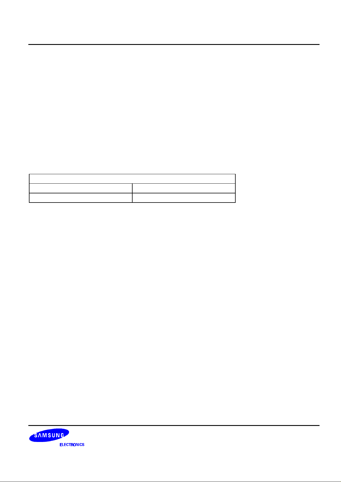
BLOCK DIAGRAM
V1
V3
V4
VEE
DISPOFFB
CL1
D0
D1
D2
D3
CL2
EIB
S1S2S3
80 bit 4- Level Driver
M
Power Down
Function
80 bit Level Shifter
80 bit Data Latch
20 x 4 bit Bidirectional Register
Shift CL
S78
S79
S80
SHL
VDD
VSS
EOB
2
80CH SEGMENT DRIVER FOR DOT MATRIX LCD
S6B2104
PIN CONFIGURATION
SC30
SC29
8079787776757473727170696867666564636261605958575655545352
SC31
SC32
SC33
SC34
SC35
SC36
SC37
SC38
SC39
SC40
SC41
SC42
SC43
SC44
SC45
SC46
SC47
SC48
SC49
SC50
81
82
83
84
85
86
87
88
89
90
91
92
93
94
95
96
97
98
99
100
1234567891011121314151617181920212223242526272829
SC28
SC27
SC26
SC25
SC24
SC23
SC22
SC21
SC20
SC19
SC18
SC17
SC16
S6B2104
SC15
SC14
SC13
SC12
SC11
SC10S9S8S7S6S5S4S3S2
S1
51
50
49
48
47
46
45
44
43
42
41
40
39
38
37
36
35
34
33
32
31
30
EIB
CL1
NC
CL2
D0
D1
D2
D3
VSS
SHL
VDD
DISPOFFB
M
NC
V1
V3
V4
VEE
NC
EOB
SC51
SC52
SC53
SC54
SC55
SC56
SC57
SC58
SC59
SC60
SC61
SC62
SC63
SC64
SC65
SC66
SC67
SC68
SC69
SC70
SC71
SC72
SC73
SC74
SC75
SC76
SC77
SC78
SC79
SC80
3
S6B2104 80CH SEGMENT DRIVER FOR DOT MATRIX LCD
MAXIMUM ABSOLUTE LIMIT
Characteristic Symbol Value Unit
Operating voltage
Driver supply voltage
Input voltage
Operating temperature
Storage temperature
Voltage greater than above may result in damage to the circuit.
VDD
V
LCD
VIN
T
OPR
T
STG
-0.3 - 6.0 V
0 - 30
-0.3 - VDD +0.3
-30 - +85
°C
-55 - +150
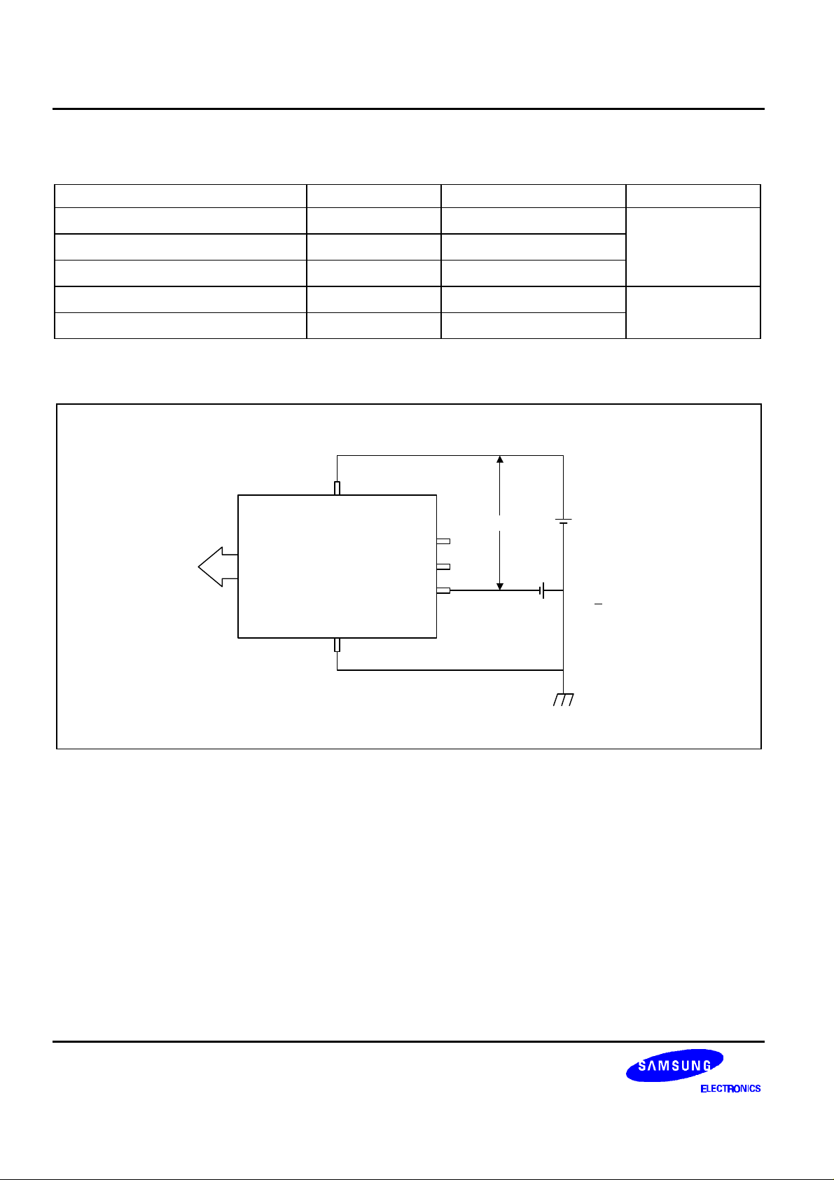
VDD (V1)
VDD-VEE
V3
S1 - S80To LCD Panel
S6B2104
VSS
V4
VEE
+V
V1 > V3 > V4 > VEE
V1 < VDD
-V
4

80CH SEGMENT DRIVER FOR DOT MATRIX LCD
ELECTRICAL CHARACTERISTICS
S6B2104
DC Characteristics
(VDD = 2.7 to 5.5V, VSS = 0V, Ta = -30 to +85°C, CL = 15pF)
Characteristics Symbol
Operating voltage
Driver supply voltage
Input voltage
Output voltage
(1)
(2)
Input leakage
current 1
(1)
Input leakage
current 2
On resistance
(3)
(4)
Supply current
VDD
V
LCD
V
LCD
VIH
VIL
VOH IOH = -0.4mA
VOL IOL = 0.4mA
I
VIN = VDD to VSS
IL1
I
VIN = VDD to VEE
IL2
RON
I
STB
IDD
ION = 100µA
fCL2 = 1MHz,
fCL2 = 19.2kHz,
fM = 40Hz,
Condition Min Typ Max Unit
- 2.7 - 5.5 V
= VDD - VEE
- 0.8VDD
- 0 - 0.2VDD
VDD = 5.5V
VDD = 5.5V
VDD = 2.7V
VLCD = 26V
IEE
No Load
VDD = 5.5V
(5)
(6)
(6)
(7)
6 - 28
- -
VDD-0.4
- - V
- - 0.4
-1 - 1
-25 - 25
- 2 4
- - 200
- - 3 mA
- - 1 mA
- 150 500
µA
kΩ
µA
µA
NOTES:
1. Applied to CL1, CL2, EIB, EOB, D0 to D3, SHL, DISPOFFB, M pin.
2. EIB, EOB pin
3. V1, V3, V4 pin
4. VDD-VEE = 26V(VDD = 3V), VEE = 28V(VDD = 5V), V1 = VDD, V3 = VDD-2/10(VDD-VEE), V4 = VEE+2/10(VDD-VEE),
S1 to S80 pin
5. Display data pattern: 0000, Current from VDD to VSS when the display data is not processing (SHL = VSS, D0 to D3 =
VSS, DISPOFFB = VDD, M = VSS)
6. Display data pattern: 1010, Current from VDD to VSS when the display data is processing
7. Display data pattern: 1010, Current on VEE pin
5

S6B2104 80CH SEGMENT DRIVER FOR DOT MATRIX LCD
AC Characteristics
(VDD = +5V ± 10%, VSS = 0V, Ta = -30 to +85
Characteristic Symbol Condition Min Typ Max Unit
t
Clock cycle time
Clock pulse width
Clock rise/fall time
Data set-up time
Data hold time
Clock set-up time1
Clock set-up time2
Clock hold time
Propagation delay time
CYC
tW
tR/tF
tDS
tDH
T
CS1
T
CS2
tCH
t
PHL
t
EIB, EOB set-up time
PSU
°
C, C
= 15pF)
L
Duty = 50% 125 - - ns
- 45 - -
- - - 30
- 30 - -
- 30 - -
- 80 - -
- 10 - -
- 80 - -
EOB output - - 80
EIB output 80
EOB input 30 - -
EIB input 30
(VDD = +3V ± 10%, VSS = 0V, Ta = -30 to +85°C, CL = 15pF)
Characteristic Symbol Condition Min Typ Max Unit
t
Clock cycle time
Clock pulse width
Clock rise/fall time
Data set-up time
Data hold time
Clock set-up time1
Clock set-up time2
Clock hold time
Propagation delay time
EIB, EOB set-up time
CYC
tW
tR/tF
tDS
tDH
T
CS1
t
CS2
tCH
t
PHL
t
PSU
Duty = 50% 250 - - ns
- 95 - -
- - - 30
- 50 - -
- 50 - -
- 80
- 15 - -
- 120 - -
EOB output - - 155
EIB output 155
EOB input 65 - -
EIB input 65
6

80CH SEGMENT DRIVER FOR DOT MATRIX LCD
Timing Characteristics
tw tw twtF
S6B2104
CL2
D0 to D3
CL1
CL2
CL1
EOB, EIB
(output)
EIB, EOB
(input)
0.8VDD
0.2VDD 0.2VDD
tDS tDH
0.8VDD
tCS2
1 2 19 20
0.2VDD
tCS1
0.8VDD
tw
tR tF
~
~
~
~
~
~
~
~
tCH
0.2VDD
0.2VDD
tPHL
0.8VDD
0.8VDD
0.2VDD
tPUS
7

S6B2104 80CH SEGMENT DRIVER FOR DOT MATRIX LCD
selected by V1 level
PIN DESCRIPTION
Table 1. Pin Description
Pin No I/O Name Function Interface
VDD (40) Power Operating voltage
For logical circuit (+5V ± 10%, +3V ± 10%)
VSS (42) 0V (GND) Power
VEE (33) Negative supply
For LCD drive circuit Supply
voltage
V1, V3, V4
(34-36)
I LCD driver output
voltage level
Bias supply voltage terminals to drive the LCD.
Bias voltage divided by the resistance is usually used
as supply voltage source. (refer to note 1)
S1-S80
(1-30,
51-100)
O LCD driver output Display data output pin which corresponds to the
respective latch contents. One of V1, V3, V4 and VEE
is selected as a display driving voltage source
according to the combination of the latched data level
and M signal (refer to note 2)
CL2 (47) I Data shift clock Clock pulse input for the 4 bit parallel shift register.
The data is shifted to 80 bit shift register at the falling
edge of the clock pulse. The clock pulse, which was
input when the enable bit (EIB/EOB) is not active
condition, is invalid.
M (38) I Alternate signal for
LCD driver output
Alternate signal input pin for LCD driving.
Normal frame inversion signal is input
CL1 (49) I Data latch clock The signal for latching the shift register contents is
input to this terminal. CL1 pulse "H" level initializes
power-down function block.
DISPOFFB
(39)
I Output level
control
(Display off)
Control input pin for display data output level (S1-
S80). V1 level is output from S1-S80 terminal during
"L" level input. LCD becomes non-
output from every output of segment drivers and every
output of common drivers.
SHL (41) I Data shift control EOB and EIB can be used as either input terminal or
output terminal according to the condition of SHL. The
shifting direction of each data, D0-D3, the I/O
condition of EOB and EIB, and the condition of SHL
are described in the table below. (refer to note 3).
Power
LCD
Controller
Controller
Controller
Controller
VDD/VSS
8

80CH SEGMENT DRIVER FOR DOT MATRIX LCD
S80
Table 1. Pin Description (Continued)
S6B2104
Pin No I/O Nam
EOB,EIB
I/O Pin I/O SHL Display data shift direction Description
(31,50)
EOB I L
EIB O
EIB
EOB O
D0-D3
(43-46)
e
I H
I EOB I L
Function Interface
D0: S1→S5…→S77
D1: S2→S6…→S78
D2: S3→S7…→S79
D3: S4→S8…→S80
D0: 80→S76…→S4
D1: 79→S75…→S3
D2: 78→S74…→S2
D3: 77→S73…→S1
S1S2S3
D0D1D2D
Enable input terminal of S6B2104.
Enable output terminal of S6B2104. EIB is
connected to next S6B2104's EOB when
the S6B2104's are connected in series
(cascade connection).
Enable input terminal of S6B2104.
Enable output terminal of S6B2104. EOB
is connected to next S6B2104's EIB when
the S6B2104's are connected in series
(cascade connection)
S4
Shift
3
S73
S74
S75
S76
S77
S78
S79
D0D1D2D3D0D1D2D
3
EIB O
EIB
EOB O
D0
D1
D2
Last Data
D3
I H
S1S2S3
D0D1D2D
First Data
S4
3
Shift Direction
S73
Shift
Shift Direction
D0D1D2D3D0D1D2D
S74
S75
S76
S77
D0
D1
D2
D3
First Data
S78
S79
S80
3
Last Data
9

S6B2104 80CH SEGMENT DRIVER FOR DOT MATRIX LCD
Display
NOTES:
1.
data input
VDD
C
C
C
C
C
Display data input pins for 4 bit parallel shift register and it is input
synchronized with the clock pulse. The combination of D0-D3 level, M
signal, display data output level and the display on the LCD panel is
described on the table below. (DISPOFFB = H)
D0-D3 M Display on the LCDDisplay Data Output Level
L L
H L
L H
H H
R
V2 (to S6B0103)
R
R
R
V5 (to S6B0103)
V1
V3
V4
V3
V1
V4
VEE
VDD
S1 - S80 To LCD Panel
S6B2104
OFF
ON
OFF
ON
Controller
2.
M Latched Data DISPOFFB Output level (S1 - S80)
L L H V3
L H H V1
H L H V4
H H H VEE
X X L V1
X: Don’t care.
C
VEE
VSS
V1, VEE
V3, V4
n = 5 (1/64 duty) to 13 (1/256 duty)
Nonselected Level
Selected Level
10

80CH SEGMENT DRIVER FOR DOT MATRIX LCD
3. - EOB and EIB pins works as input terminals.
ENABLE F/F stops display data at "H" level input. ENABLE F/F starts display data at "L" level input.
- EOB and EIB pins work as output terminals. These terminals are set to the "H" level immediately after ENABLE F/F is
initialized by the load pulse. Upon completion of 80-bit serial/parallel conversion using the shift clock input from the
CL2 terminal, these terminals are then set to the "L" level.
- The operation of ENABLE F/F is terminated and held unchanged until the next load pulse is detected. (For cascade
connection, refer to the application circuit drawing)
S6B2104
POWER DOWN FUNCTION
In order to reduce the power consumption, in case of cascade connection, S6B2104 has a "power down
function".
EIB Enable input Enable L
EOB Enable output EOB of Nth driver is connected to EIB of (N+1)th driver S6B2104
Disable H
.
CL1
CL2
1st EIB (input)
1st EOB (output)
Shift CL2
2nd EIB (input)
2nd EOB (output)
Shift CL2
~
~
1 2 19 20 1 2 19 20 20
~
~
~
~
~
~
~
~
~
~
1 2 19 20
~
~
~
~
~
~
~
~
~
~
~
~
~
~
~
~
~
~
~
~
~
~
~
~
~
~
~
~
~
~
SHL = H (EIB = Input, EOB = Output)
First S6B2104’s EOB should be connected to second S6B2104’s EIB.
11

S6B2104 80CH SEGMENT DRIVER FOR DOT MATRIX LCD
Timing Chart - 1/200 Duty, 1/15 Bias
200 1 2 200 1 2 200 1 2
CL1
Latched Data
M
M
CL1
D0 - D3
CL2
Latched Data
CL1
Latched Data
M
VDD (V1)
V2
V3
V4
V5
VEE (V6)
200
L L
H
2 200 1 2 200 1 2
L L
H
L L
H
V1 = VDD
V4 = VDD-8/10V
V2 = VDD-1/10V
V5 = VDD-9/10V
LCD
V3 = VDD-2/10V
LCD
V
LCD
LCD
= VDDVEE
LCD
12
 Loading...