

Page 1

S6C1652
written permission of LCD Driver IC Team.
6 BIT 300 / 309 CHANNEL TFT-LCD SOURCE DRIVER
August. 1999.
Ver. 0.0
Prepared by: Dae-Young, Ahn
Mail: [email protected]
Contents in this document are subject to change without notice. No part of this document may be reproduced
or transmitted in any form or by any means, electronic or mechanical, for any purpose, without the express
Page 2

S6C1652 6 BIT 300 / 309 CHANNEL TFT-LCD SOURCE DRIVER
S6C1652 Specification Revision History
Version Content Date
0.0 Original Aug.1999
2
Page 3

6 BIT 300 / 309 CHANNEL TFT-LCD SOURCE DRIVER S6C1652
CONTENTS
INTRODUCTION.................................................................................................................................................4
FEATURES......................................................................................................................................................... 4
BLOCK DIAGRAM..............................................................................................................................................5
PIN ASSIGNMENTS............................................................................................................................................6
PIN DESCRIPTIONS...........................................................................................................................................7
OPERATION DESCRIPTION.............................................................................................................................. 8
DISPLAY DATA TRANSFER............................................................................................................................ 8
EXTENSION OF OUTPUT...............................................................................................................................8
RELATIONSHIP BETWEEN INPUT DATA VALUE AND OUTPUT VOLTAGE.................................................8
ABSOLUTE MAXIMUM RATINGS....................................................................................................................15
RECOMMENDED OPERATION CONDITIONS.................................................................................................15
DC CHARACTERISTICS................................................................................................................................... 16
AC CHARACTERISTICS ................................................................................................................................... 17
WAVEFORMS...................................................................................................................................................18
RELATIONSHIPS BETWEEN CLK1, START PULSE (DIO1, DIO2) AND BLANKING PERIOD ....................... 19
3
Page 4

S6C1652 6 BIT 300 / 309 CHANNEL TFT-LCD SOURCE DRIVER
INTRODUCTION
The S6C1652 is a 300 / 309 channel output, TFT-LCD source driver for an 64 gray-scale LCD panel. Data input
is based on digital input consisting of 6 bits by 3 dots, which can realize a full-color display of 260,000 color by
output of 64 values gamma-corrected.
This device has an internal D/A (digital-to-analog) converter for each output and 18 (9-by-2) reference voltages.
Because the output dynamic range is as large as 6.0 - 12.6 Vp-p, it is unnecessary to operate level inversion of
the LCD's common electrode. Besides, to be able to deal with dot-line inversion when mounted on a single-side,
output gray-scale voltages with different polarity can be output to the odd number output pins and the even output
pins.
S6C1652 can be adopted to larger panel, and SHL (shift direction selection) pin makes the use of the LCD panel
connection conveniently. Maximum operation clock frequency is 55 MHz at 2.7 V logic operation, single edge
and it can be applied to the TFT-LCD panel of SVGA to XGA standard.
FEATURES
• TFT active matrix LCD source driver LSI
• 64 gray-scale is possible through 18 (9-by-2) reference voltages and D/A converter
• Dot inversion display is possible
• CMOS level input
• Compatible with gamma-correction
• Input of 6bits (gray-scale data) by 3 dots (R,G,B)
• Logic supply voltage: 2.7 - 3.6 V
• LCD driver supply voltage: 6.4 - 13.0 V
• Output dynamic range: 6.0 - 12.6 Vp-p
• Maximum operating frequency: fMAX = 55 MHz (internal data transmission rate at 2.7 V operation)
• Output: 300 / 309 outputs
• TCP available
4
Page 5

6 BIT 300 / 309 CHANNEL TFT-LCD SOURCE DRIVER S6C1652
Y001
BLOCK DIAGRAM
TESTB
POL
VGMA1 -
VGMA18
CLK1
BIAS
18
Y309
6 6 6 6 6 6
6 6 6 6 6 6
Y308
Y307
Output Buffer
D/A Converter
Data Latch
Y003
Y002
Data Register
6 6 6 6 6 6
D00 - D05
D10 - D15
D20 - D25
CLK2
6
6
6
18
Data Control
103bit Shift Register
DIO2 DIO1
SHL
Figure 1. S6C1652 Block Diagram
5
Page 6

S6C1652 6 BIT 300 / 309 CHANNEL TFT-LCD SOURCE DRIVER
PIN ASSIGNMENTS
Y001
Y002
Y003
Y004
Y306
Y307
Y308
Y309
(Top View)
S6C1652
VSS2
VDD2
VSS1
D05
D04
D03
D02
D01
D00
D15
D14
D13
D12
D11
D10
DIO1
VGMA1
VGMA2
VGMA3
VGMA4
VGMA5
VGMA6
VGMA7
VGMA8
VGMA9
VGMA10
VGMA11
VGMA12
VGMA13
VGMA14
VGMA15
VGMA16
VGMA17
VGMA18
SELT
CLK2
DIO2
CLK1
POL
D25
D24
D23
D22
D21
D20
SHL
TESTB
VDD1
VDD2
VSS2
Figure 2. S6C1652 Pin Assignments
6
Page 7
6 BIT 300 / 309 CHANNEL TFT-LCD SOURCE DRIVER S6C1652
g characteristic
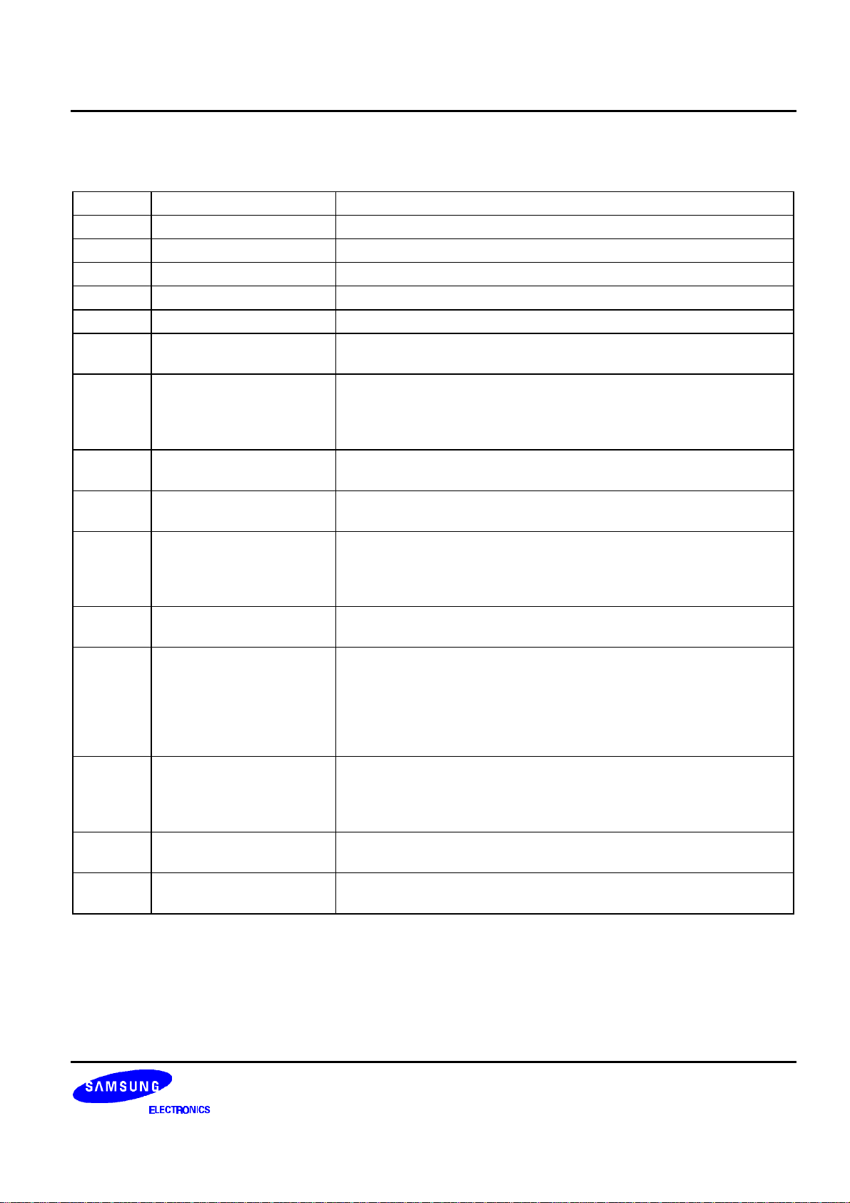
PIN DESCRIPTIONS
Symbol
VDD1 Logic power supply 2.7 - 3.6 V
VDD2 Driver power supply 6.4 - 13.0 V
VSS1 Logic ground Ground (0 V)
VSS2 Driver ground Ground (0 V)
Y1 - Y309
D0<0:5>
- D2<0:5>
SHL Shift direction control input
DIO1 Start pulse input / output
DIO2 Start pulse input / output
POL Polarity input
CLK2 Shift clock input
CLK1 Latch input
VGMA1
–
VGMA18
SELT Output selection input
TESTB Test input
Gamma corrected power
Pin Name Description
Driver outputs The D/A converted 64 gray-scale analog voltage is output.
Display data input
supplies
The display data is input with a width of 18 bits,
gray-scale data (6 bits) by 3 dots (R,G,B) DX0: LSB, DX5: MSB
This pin controls the direction of shift register in cascade connection.
The shift direction of the shift registers is as follows.
SHL = H: DIO1 input, Y1 → Y309, DIO2 output
SHL = L: DIO2 input, Y309 → Y1, DIO1 output
SHL = H: Used as the start pulse input pin
SHL = L: Used as the start pulse output pin
SHL = H: Used as the start pulse output pin
SHL = L: Used as the start pulse input pin
POL = H: The reference voltage for odd number outputs are VGMA1 –
VGMA9 and those for even number outputs are VGMA10 – VGMA18
POL = L: The reference voltage for odd number outputs are VGMA10
– VGMA18 and those for even number outputs are VGMA1 – VGMA9
Refer to the shift register's shift clock input. The display data is loaded
to the data register at the rising edge of CLK2.
Latches the contents of the data register at rising edge and transfers
them to the D/A converter. Also, after CLK1 input, clears the internal
shift register contents. After 1 pulse input on start, operates normally.
CLK1 input timing refers to the "Relationships between CLK1 start
pulse (DIO1, DIO2) and blanking period" of the switchin
waveform. Outputs the gray-scale data at rising edge.
Input the gamma corrected power supplies from external source.
VDD2 > VGMA1 > VGMA2 > ……… > VGMA17 > VGMA18 > VSS2
Keep gray-scale power supply unchanged during the gray-scale
voltage output.
SELT = H: 300 Output (Y151 - Y159 are disabled)
SELT = L: 309 Output
TESTB = H: Normal operation mode
TESTB = L: Test mode (OP AMP CUT-OFF, Rpu = 30kΩ)
7
Page 8

S6C1652 6 BIT 300 / 309 CHANNEL TFT-LCD SOURCE DRIVER
OPERATION DESCRIPTION
DISPLAY DATA TRANSFER
When DIO1 (or DIO2) pulse is loaded into internal latch on the rising edge of CLK2, DIO1 (or DIO2) pulse
enables the data transfer operation. After the falling edge of DIO1 (or DIO2), display data is valid on the rising
edge of CLK2. Once all the data of 300 / 309 channels are loaded into internal latch, it goes into stand-by state
automatically, and any new data is not accepted even though CLK2 is provided until next DIO1 (or DIO2)
input. When next DIO1 (or DIO2) is provided, new display data is valid on the next rising edge of CLK2 after
the falling edge of DIO1 (or DIO2).
EXTENSION OF OUTPUT
Output pin can be adjusted to an extended screen by cascade connection.
(1) SHL = "L"
Connect DIO1 pin of previous stage to the DIO2 pin of next stage and all the input pins
except DIO1 and DIO2 are connected together in each device.
(2) SHL = "H"
Connect DIO2 pin of previous stage to the DIO1 pin of next stage and all the input pins
except DIO2 and DIO1 are connected together in each device.
RELATIONSHIP BETWEEN INPUT DATA VALUE AND OUTPUT VOLTAGE
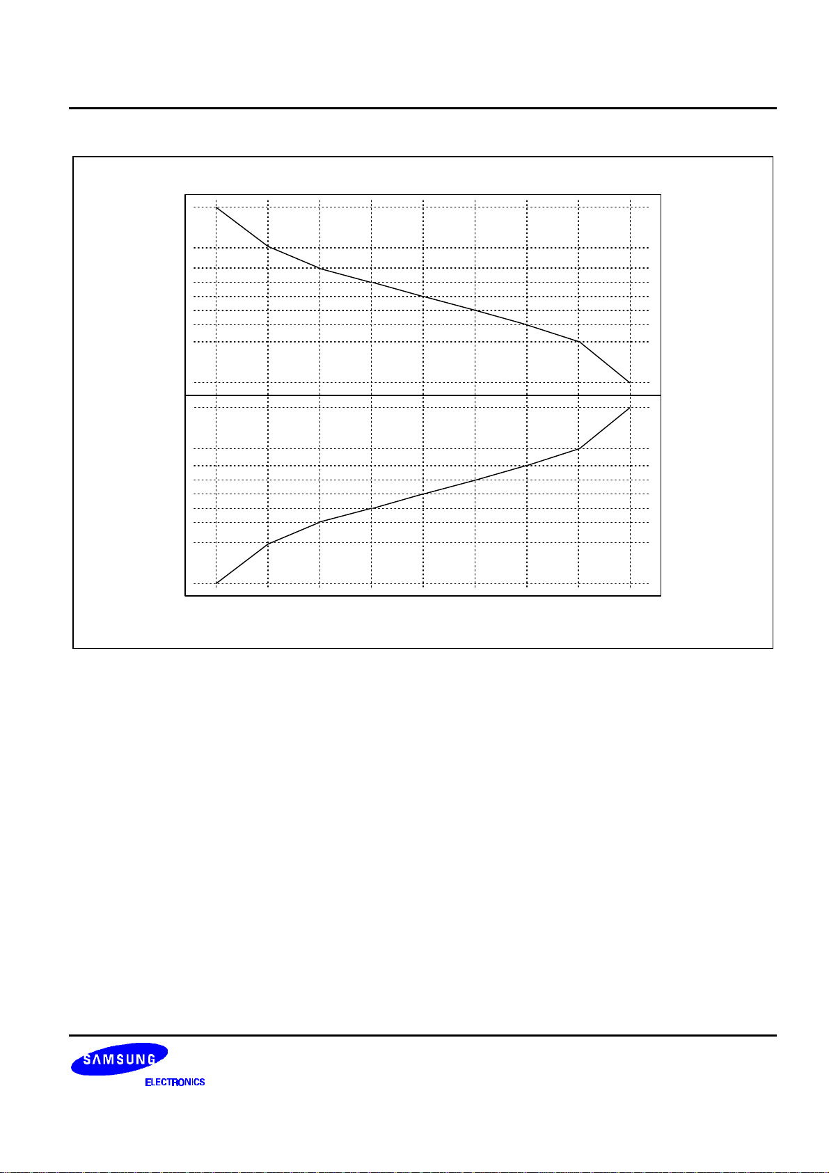
The LCD drive output voltages are determined by the input data and 18 (9-by-2) gamma corrected power
supplies (VGMA1 - VGMA18). Besides, to be able to deal with dot-line inversion when mounted on a singleside, gradation voltages with different polarity can be output to the odd number output pins and the even
number output pins. Among 9-by-2 gamma corrected voltages, input gray-scale voltages of the same polarity
with respect to the common voltage, for the respective 9 gamma corrected voltages of VGMA1 - VGMA9 and
VGMA10 - VGMA18.
SHL = H
OUTPUT
-
DATA
Y1 Y2
First Last
D00 - D05 D10 - D15 D20 - D25
Y3
SHL = L
OUTPUT Y3
Y1 Y2 ......
...... Y307 Y308 Y309
......
D00 - D05 D10 - D15 D20 - D25
Y307 Y308 Y309
Last
D00 - D05 D10 - D15 D20 - D25 ......DATA
D00 - D05 D10 - D15 D20 - D25
First-
Figure 3. Relationship between Shift Direction and Output Data
8
Page 9
6 BIT 300 / 309 CHANNEL TFT-LCD SOURCE DRIVER S6C1652
VDD2
VGMA1
VGMA2
VGMA3
VGMA4
VGMA5
VGMA6
VGMA7
VGMA8
VGMA9
VGMA10
VGMA11
VGMA12
VGMA13
VGMA14
VGMA15
VGMA16
VGMA17
VGMA18
VSS2
00H 08H 10H 18H 20H 28H 30H 38H 3FH
Figure 4. Gamma Correction Curve
VCOM
Input data
9
Page 10
S6C1652 6 BIT 300 / 309 CHANNEL TFT-LCD SOURCE DRIVER
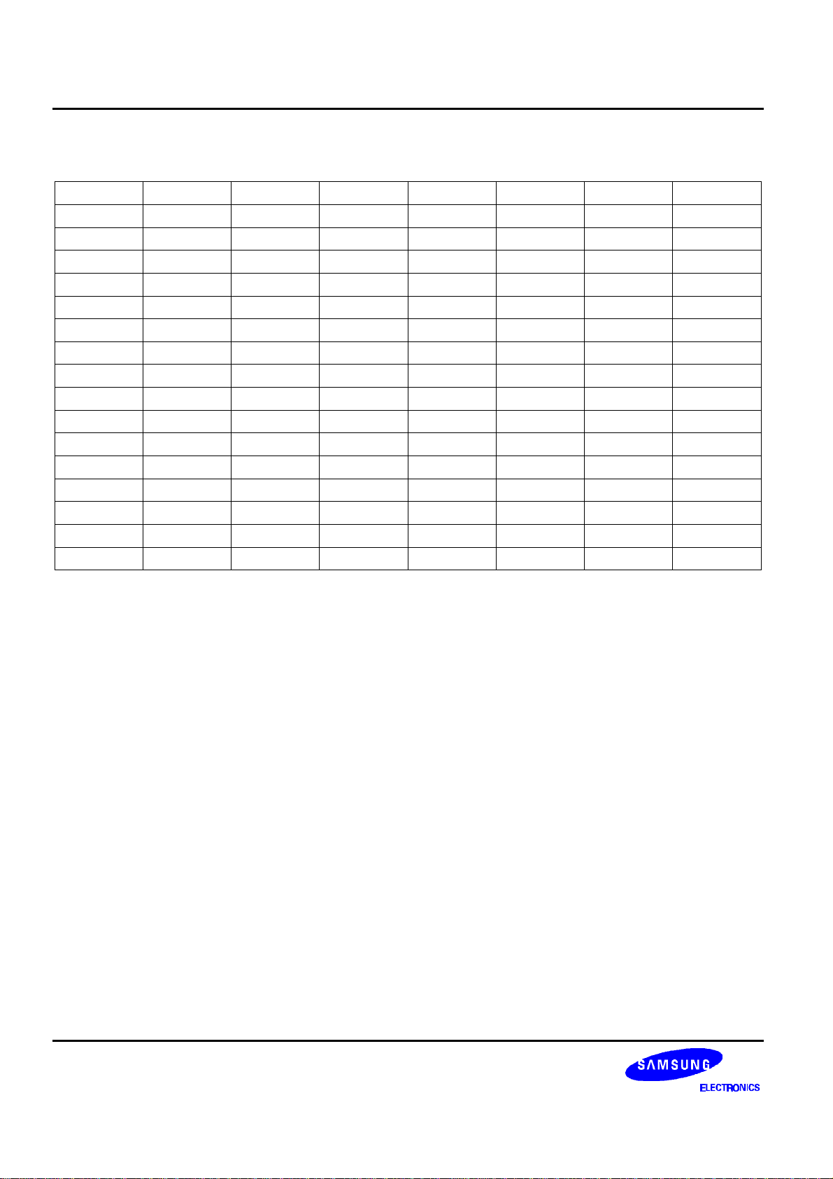
Table 1. Resistor Strings (R0 - R63, unit: Ω)
Name Value Name Value Name Value Name Value
R0 510 R16 170 R32 170 R48 255
R1 510 R17 170 R33 170 R49 255
R2 510 R18 170 R34 170 R50 255
R3 510 R19 170 R35 170 R51 255
R4 510 R20 170 R36 170 R52 255
R5 510 R21 170 R37 170 R53 255
R6 510 R22 170 R38 170 R54 255
R7 510 R23 170 R39 170 R55 255
R8 255 R24 170 R40 170 R56 510
R9 255 R25 170 R41 170 R57 510
R10 255 R26 170 R42 170 R58 510
R11 255 R27 170 R43 170 R59 510
R12 255 R28 170 R44 170 R60 510
R13 255 R29 170 R45 170 R61 510
R14 255 R30 170 R46 170 R62 510
R15 255 R31 170 R47 170 R63 510
10
Page 11
6 BIT 300 / 309 CHANNEL TFT-LCD SOURCE DRIVER S6C1652
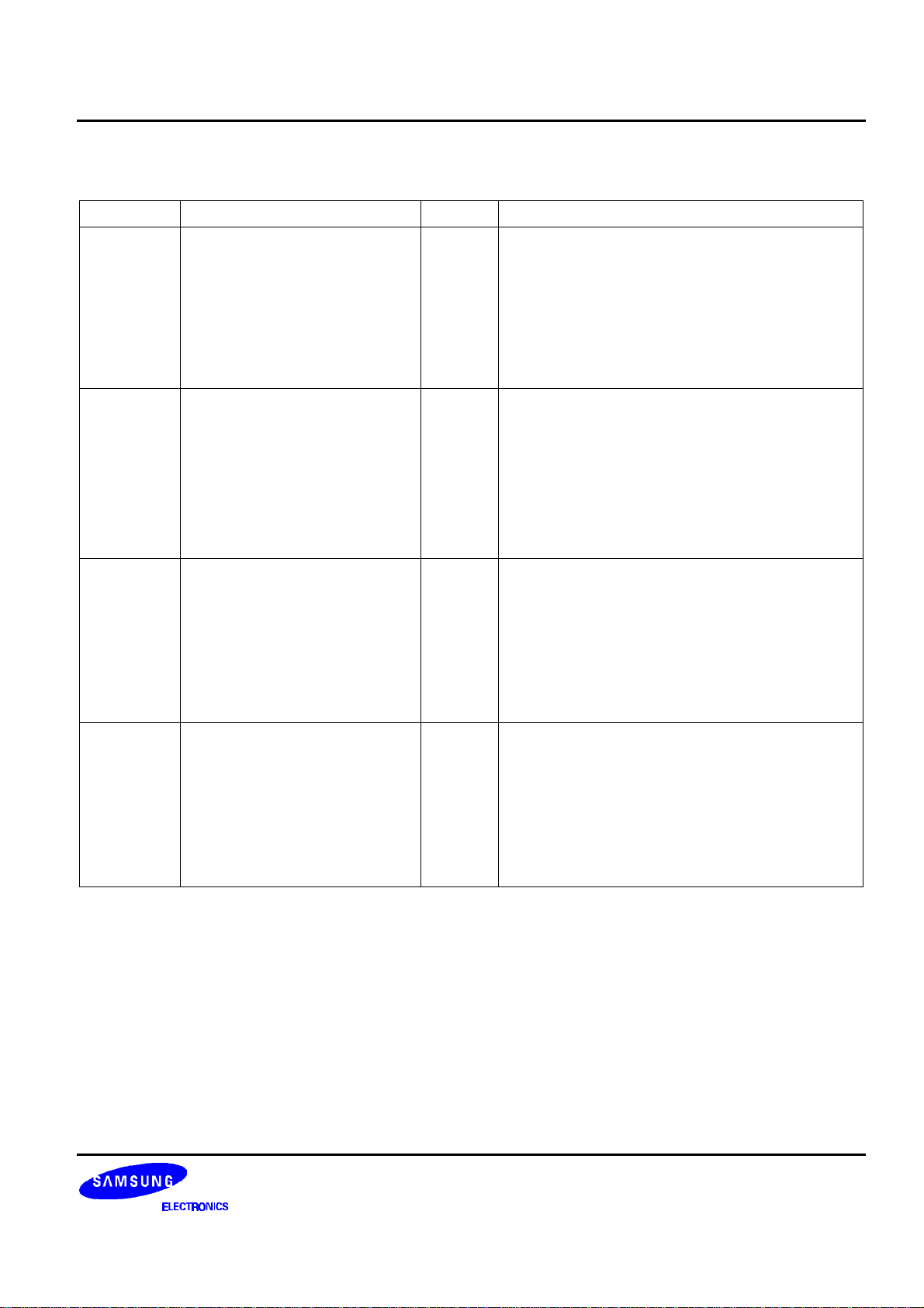
Table 2. Relationship between Input Data and Output Voltage Value
Input data
00H
01H
02H
03H
04H
05H
06H
07H
08H
09H
0AH
0BH
0CH
0DH
0EH
0FH
10H
11H
12H
13H
14H
15H
16H
17H
18H
19H
1AH
1BH
1CH
1DH
1EH
1FH
DX5 DX4 DX3 DX2 DX1 DX0
0 0 0 0 0 0
0 0 0 0 0 1
0 0 0 0 1 0
0 0 0 0 1 1
0 0 0 1 0 0
0 0 0 1 0 1
0 0 0 1 1 0
0 0 0 1 1 1
0 0 1 0 0 0
0 0 1 0 0 1
0 0 1 0 1 0
0 0 1 0 1 1
0 0 1 1 0 0
0 0 1 1 0 1
0 0 1 1 1 0
0 0 1 1 1 1
0 1 0 0 0 0
0 1 0 0 0 1
0 1 0 0 1 0
0 1 0 0 1 1
0 1 0 1 0 0
0 1 0 1 0 1
0 1 0 1 1 0
0 1 0 1 1 1
0 1 1 0 0 0
0 1 1 0 0 1
0 1 1 0 1 0
0 1 1 0 1 1
0 1 1 1 0 0
0 1 1 1 0 1
0 1 1 1 1 0
0 1 1 1 1 1
G/S Output voltage
VH0
VH1
VH2
VH3
VH4
VH5
VH6
VH7
VH8
VH9
VH10
VH11
VH12
VH13
VH14
VH15
VH16
VH17
VH18
VH19
VH20
VH21
VH22
VH23
VH24
VH25
VH26
VH27
VH28
VH29
VH30
VH31
VGMA1 + (VGMA2 - VGMA1) × 1 / 8
VGMA1 + (VGMA2 - VGMA1) × 2 / 8
VGMA1 + (VGMA2 - VGMA1) × 3 / 8
VGMA1 + (VGMA2 - VGMA1) × 4 / 8
VGMA1 + (VGMA2 - VGMA1) × 5 / 8
VGMA1 + (VGMA2 - VGMA1) × 6 / 8
VGMA1 + (VGMA2 - VGMA1) × 7 / 8
VGMA2 + (VGMA3 - VGMA2) × 1 / 8
VGMA2 + (VGMA3 - VGMA2) × 2 / 8
VGMA2 + (VGMA3 - VGMA2) × 3 / 8
VGMA2 + (VGMA3 - VGMA2) × 4 / 8
VGMA2 + (VGMA3 - VGMA2) × 5 / 8
VGMA2 + (VGMA3 - VGMA2) × 6 / 8
VGMA2 + (VGMA3 - VGMA2) × 7 / 8
VGMA3 + (VGMA4 - VGMA3) × 1 / 8
VGMA3 + (VGMA4 - VGMA3) × 2 / 8
VGMA3 + (VGMA4 - VGMA3) × 3 / 8
VGMA3 + (VGMA4 - VGMA3) × 4 / 8
VGMA3 + (VGMA4 - VGMA3) × 5 / 8
VGMA3 + (VGMA4 - VGMA3) × 6 / 8
VGMA3 + (VGMA4 - VGMA3) × 7 / 8
VGMA4 + (VGMA5 - VGMA4) × 1 / 8
VGMA4 + (VGMA5 - VGMA4) × 2 / 8
VGMA4 + (VGMA5 - VGMA4) × 3 / 8
VGMA4 + (VGMA5 - VGMA4) × 4 / 8
VGMA4 + (VGMA5 - VGMA4) × 5 / 8
VGMA4 + (VGMA5 - VGMA4) × 6 / 8
VGMA4 + (VGMA5 - VGMA4) × 7 / 8
VGMA1
VGMA2
VGMA3
VGMA4
NOTE: VDD2>VGMA1>VGMA2>VGMA3>VGMA4>VGMA5>VGMA6>VGMA7>VGMA8>VGMA9
11
Page 12
S6C1652 6 BIT 300 / 309 CHANNEL TFT-LCD SOURCE DRIVER
Table 2. Relationship between Input Data and Output Voltage Value (Continued)
Input data
20H
21H
22H
23H
24H
25H
26H
27H
28H
29H
2AH
2BH
2CH
2DH
2EH
2FH
30H
31H
32H
33H
34H
35H
36H
37H
38H
39H
3AH
3BH
3CH
3DH
3EH
3FH
DX5 DX4 DX3 DX2 DX1 DX0
1
1
1
1
1
1
1
1
0 0 0 0 0
0 0 0 0 1
0 0 0 1 0
0 0 0 1 1
0 0 1 0 0
0 0 1 0 1
0 0 1 1 0
0 0 1 1 1
1 0 1 0 0 0
1 0 1 0 0 1
1 0 1 0 1 0
1 0 1 0 1 1
1 0 1 1 0 0
1 0 1 1 0 1
1 0 1 1 1 0
1 0 1 1 1 1
1 1 0 0 0 0
1 1 0 0 0 1
1 1 0 0 1 0
1 1 0 0 1 1
1 1 0 1 0 0
1 1 0 1 0 1
1 1 0 1 1 0
1 1 0 1 1 1
1 1 1 0 0 0
1 1 1 0 0 1
1 1 1 0 1 0
1 1 1 0 1 1
1 1 1 1 0 0
1 1 1 1 0 1
1 1 1 1 1 0
1 1 1 1 1 1
G/S Output voltage
VH32
VH33
VH34
VH35
VH36
VH37
VH38
VH39
VH40
VH41
VH42
VH43
VH44
VH45
VH46
VH47
VH48
VH49
VH50
VH51
VH52
VH53
VH54
VH55
VH56
VH57
VH58
VH59
VH60
VH61
VH62
VH63
VGMA5 + (VGMA6 - VGMA5) × 1 / 8
VGMA5 + (VGMA6 - VGMA5) × 2 / 8
VGMA5 + (VGMA6 - VGMA5) × 3 / 8
VGMA5 + (VGMA6 - VGMA5) × 4 / 8
VGMA5 + (VGMA6 - VGMA5) × 5 / 8
VGMA5 + (VGMA6 - VGMA5) × 6 / 8
VGMA5 + (VGMA6 - VGMA5) × 7 / 8
VGMA6 + (VGMA7 - VGMA6) × 1 / 8
VGMA6 + (VGMA7 - VGMA6) × 2 / 8
VGMA6 + (VGMA7 - VGMA6) × 3 / 8
VGMA6 + (VGMA7 - VGMA6) × 4 / 8
VGMA6 + (VGMA7 - VGMA6) × 5 / 8
VGMA6 + (VGMA7 - VGMA6) × 6 / 8
VGMA6 + (VGMA7 - VGMA6) × 7 / 8
VGMA7 + (VGMA8 - VGMA7) × 1 / 8
VGMA7 + (VGMA8 - VGMA7) × 2 / 8
VGMA7 + (VGMA8 - VGMA7) × 3 / 8
VGMA7 + (VGMA8 - VGMA7) × 4 / 8
VGMA7 + (VGMA8 - VGMA7) × 5 / 8
VGMA7 + (VGMA8 - VGMA7) × 6 / 8
VGMA7 + (VGMA8 - VGMA7) × 7 / 8
VGMA8 + (VGMA9 - VGMA8) × 1 / 8
VGMA8 + (VGMA9 - VGMA8) × 2 / 8
VGMA8 + (VGMA9 - VGMA8) × 3 / 8
VGMA8 + (VGMA9 - VGMA8) × 4 / 8
VGMA8 + (VGMA9 - VGMA8) × 5 / 8
VGMA8 + (VGMA9 - VGMA8) × 6 / 8
VGMA8 + (VGMA9 - VGMA8) × 7 / 8
VGMA5
VGMA6
VGMA7
VGMA8
12
Page 13
6 BIT 300 / 309 CHANNEL TFT-LCD SOURCE DRIVER S6C1652
Table 2. Relationship between Input Data and Output Voltage Value (Continued)
Input data
00H
01H
02H
03H
04H
05H
06H
07H
08H
09H
0AH
0BH
0CH
0DH
0EH
0FH
10H
11H
12H
13H
14H
15H
16H
17H
18H
19H
1AH
1BH
1CH
1DH
1EH
1FH
DX5 DX4 DX3 DX2 DX1 DX0
0 0 0 0 0 0
0 0 0 0 0 1
0 0 0 0 1 0
0 0 0 0 1 1
0 0 0 1 0 0
0 0 0 1 0 1
0 0 0 1 1 0
0 0 0 1 1 1
0 0 1 0 0 0
0 0 1 0 0 1
0 0 1 0 1 0
0 0 1 0 1 1
0 0 1 1 0 0
0 0 1 1 0 1
0 0 1 1 1 0
0 0 1 1 1 1
0 1 0 0 0 0
0 1 0 0 0 1
0 1 0 0 1 0
0 1 0 0 1 1
0 1 0 1 0 0
0 1 0 1 0 1
0 1 0 1 1 0
0 1 0 1 1 1
0 1 1 0 0 0
0 1 1 0 0 1
0 1 1 0 1 0
0 1 1 0 1 1
0 1 1 1 0 0
0 1 1 1 0 1
0 1 1 1 1 0
0 1 1 1 1 1
G/S Output voltage
VL0
VL1
VL2
VL3
VL4
VL5
VL6
VL7
VL8
VL9
VL10
VL11
VL12
VL13
VL14
VL15
VL16
VL17
VL18
VL19
VL20
VL21
VL22
VL23
VL24
VL25
VL26
VL27
VL28
VL29
VL30
VL31
VGMA18 + (VGMA17 - VGMA18) × 1 / 8
VGMA18 + (VGMA17 - VGMA18) × 2 / 8
VGMA18 + (VGMA17 - VGMA18) × 3 / 8
VGMA18 + (VGMA17 - VGMA18) × 4 / 8
VGMA18 + (VGMA17 - VGMA18) × 5 / 8
VGMA18 + (VGMA17 - VGMA18) × 6 / 8
VGMA18 + (VGMA17 - VGMA18) × 7 / 8
VGMA17 + (VGMA16 - VGMA17) × 1 / 8
VGMA17 + (VGMA16 - VGMA17) × 2 / 8
VGMA17 + (VGMA16 - VGMA17) × 3 / 8
VGMA17 + (VGMA16 - VGMA17) × 4 / 8
VGMA17 + (VGMA16 - VGMA17) × 5 / 8
VGMA17 + (VGMA16 - VGMA17) × 6 / 8
VGMA17 + (VGMA16 - VGMA17) × 7 / 8
VGMA16 + (VGMA15 - VGMA16) × 1 / 8
VGMA16 + (VGMA15 - VGMA16) × 2 / 8
VGMA16 + (VGMA15 - VGMA16) × 3 / 8
VGMA16 + (VGMA15 - VGMA16) × 4 / 8
VGMA16 + (VGMA15 - VGMA16) × 5 / 8
VGMA16 + (VGMA15 - VGMA16) × 6 / 8
VGMA16 + (VGMA15 - VGMA16) × 7 / 8
VGMA15 + (VGMA14 - VGMA15) × 1 / 8
VGMA15 + (VGMA14 - VGMA15) × 2 / 8
VGMA15 + (VGMA14 - VGMA15) × 3 / 8
VGMA15 + (VGMA14 - VGMA15) × 4 / 8
VGMA15 + (VGMA14 - VGMA15) × 5 / 8
VGMA15 + (VGMA14 - VGMA15) × 6 / 8
VGMA15 + (VGMA14 - VGMA15) × 7 / 8
VGMA18
VGMA17
VGMA16
VGMA15
NOTE: VGMA10>VGMA11>VGMA12>VGMA13>VGMA14>VGMA15>VGMA16>VGMA17>VGMA18>VSS2
13
Page 14
S6C1652 6 BIT 300 / 309 CHANNEL TFT-LCD SOURCE DRIVER
Table 2. Relationship between Input Data and Output Voltage Value (Continued)
Input data
20H
21H
22H
23H
24H
25H
26H
27H
28H
29H
2AH
2BH
2CH
2DH
2EH
2FH
30H
31H
32H
33H
34H
35H
36H
37H
38H
39H
3AH
3BH
3CH
3DH
3EH
3FH
DX5 DX4 DX3 DX2 DX1 DX0
1
1
1
1
1
1
1
1
0 0 0 0 0
0 0 0 0 1
0 0 0 1 0
0 0 0 1 1
0 0 1 0 0
0 0 1 0 1
0 0 1 1 0
0 0 1 1 1
1 0 1 0 0 0
1 0 1 0 0 1
1 0 1 0 1 0
1 0 1 0 1 1
1 0 1 1 0 0
1 0 1 1 0 1
1 0 1 1 1 0
1 0 1 1 1 1
1 1 0 0 0 0
1 1 0 0 0 1
1 1 0 0 1 0
1 1 0 0 1 1
1 1 0 1 0 0
1 1 0 1 0 1
1 1 0 1 1 0
1 1 0 1 1 1
1 1 1 0 0 0
1 1 1 0 0 1
1 1 1 0 1 0
1 1 1 0 1 1
1 1 1 1 0 0
1 1 1 1 0 1
1 1 1 1 1 0
1 1 1 1 1 1
G/S Output voltage
VL32
VL33
VL34
VL35
VL36
VL37
VL38
VL39
VL40
VL41
VL42
VL43
VL44
VL45
VL46
VL47
VL48
VL49
VL50
VL51
VL52
VL53
VL54
VL55
VL56
VL57
VL58
VL59
VL60
VL61
VL62
VL63
VGMA14 + (VGMA13 - VGMA14) × 1 / 8
VGMA14 + (VGMA13 - VGMA14) × 2 / 8
VGMA14 + (VGMA13 - VGMA14) × 3 / 8
VGMA14 + (VGMA13 - VGMA14) × 4 / 8
VGMA14 + (VGMA13 - VGMA14) × 5 / 8
VGMA14 + (VGMA13 - VGMA14) × 6 / 8
VGMA14 + (VGMA13 - VGMA14) × 7 / 8
VGMA13 + (VGMA12 - VGMA13) × 1 / 8
VGMA13 + (VGMA12 - VGMA13) × 2 / 8
VGMA13 + (VGMA12 - VGMA13) × 3 / 8
VGMA13 + (VGMA12 - VGMA13) × 4 / 8
VGMA13 + (VGMA12 - VGMA13) × 5 / 8
VGMA13 + (VGMA12 - VGMA13) × 6 / 8
VGMA13 + (VGMA12 - VGMA13) × 7 / 8
VGMA12 + (VGMA11 - VGMA12) × 1 / 8
VGMA12 + (VGMA11 - VGMA12) × 2 / 8
VGMA12 + (VGMA11 - VGMA12) × 3 / 8
VGMA12 + (VGMA11 - VGMA12) × 4 / 8
VGMA12 + (VGMA11 - VGMA12) × 5 / 8
VGMA12 + (VGMA11 - VGMA12) × 6 / 8
VGMA12 + (VGMA11 - VGMA12) × 7 / 8
VGMA11 + (VGMA10 - VGMA11) × 1 / 8
VGMA11 + (VGMA10 - VGMA11) × 2 / 8
VGMA11 + (VGMA10 - VGMA11) × 3 / 8
VGMA11 + (VGMA10 - VGMA11) × 4 / 8
VGMA11 + (VGMA10 - VGMA11) × 5 / 8
VGMA11 + (VGMA10 - VGMA11) × 6 / 8
VGMA11 + (VGMA10 - VGMA11) × 7 / 8
VGMA14
VGMA13
VGMA12
VGMA11
14
Page 15
6 BIT 300 / 309 CHANNEL TFT-LCD SOURCE DRIVER S6C1652
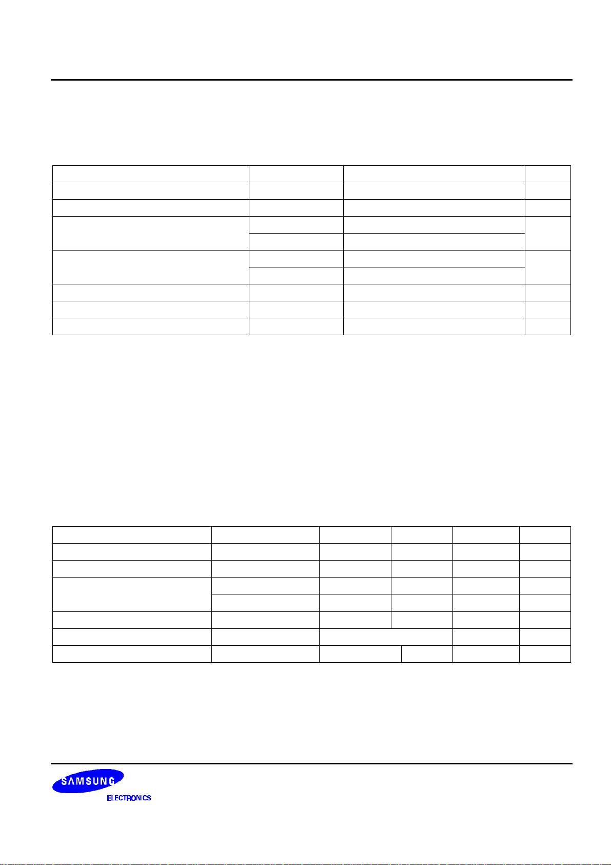
ABSOLUTE MAXIMUM RATINGS
Table 3. Absolute Maximum Ratings (VSS1 = VSS2 = 0 V)
Parameter Symbol Ratings Unit
Logic supply voltage VDD1 -0.3 to 6.5 V
Driver supply voltage VDD2 -0.3 to 15.0 V
Input voltage
Output voltage
Operating power dissipation Pd 150
Operation temperature Top -20 to 75
Storage temperature Tstg -55 to 125
NOTE: Relationship between TFT-LCD panel and Pd (Pd ∝ CL* (VDD2)2 * fCLK1)
VGMA1 - 18 -0.3 to VDD2 + 0.3
Others -0.3 to VDD1 + 0.3
DIO1, 2 -0.3 to VDD1 + 0.3
Y1 - Y309 -0.3 to VDD2 + 0.3
(1)
mW
V
V
°C
°C
CAUTIONS:
If LSIs are stressed beyond those listed above “absolute maximum ratings”, they may be permanently
destroyed. These are stress ratings only, and functional operation of the device at these or any other
condition beyond those indicated under “recommended operating conditions” is not implied. Exposure to
absolute maximum rated conditions for extended periods may affect device reliability.
Turn on power order: VDD1 → control signal input → VDD2 → VGMA1 - VGMA18
Turn off power order: VGMA1 - VGMA18 → VDD2 → control signal input → VDD1
RECOMMENDED OPERATION CONDITIONS
Table 4. Recommended Operation Conditions (Ta = -20 to 75 °C, VSS1 = VSS2 = 0 V)
Parameter Symbol Min. Typ. Max. Unit
Logic supply voltage VDD1 2.7 3.0 3.6 V
Driver supply voltage VDD2
Gamma corrected voltage
VGMA1 - VGMA9 0.5VDD2 - VDD2 - 0.2
VGMA10 - VGMA18 VSS2 + 0.2 - 0.5VDD2 V
Driver part output voltage Vyo VSS2 + 0.2 - VDD2 - 0.2
Maximum clock frequency fmax VDD1 = 2.7 V 55 MHz
Output load capacitance CL
NOTE: Relationship between TFT-LCD panel and Pd (Pd ∝ CL* (VDD2)2 * fCLK1)
(1)
6.4 9.0 13.0 V
(1)
- - 150 pF / PIN
V
V
15
Page 16

S6C1652 6 BIT 300 / 309 CHANNEL TFT-LCD SOURCE DRIVER
DC CHARACTERISTICS
Table 5. DC Characteristics (Ta = -20 to 75 °C, VDD1 = 2.7 to 3.6 V, VDD2 = 6.4 to 13.0 V, VSS1 = VSS2 =
0V)
Parameter Symbol
High level input voltage VIH 0.75VDD1 - VDD1
Low level input voltage VIL 0 - 0.25VDD1
Input leakage current IL
High level output voltage
Low level output voltage
Resistor R0 - R63
VOH DIO1 (DIO2), IO = -1.0 mA VDD1 - 0.5
VOL DIO1 (DIO2), IO = +1.0 mA
IVOH
CLK1, SELT, POL, DIO1
Refer to Table 1. Resistor
Vx = 2.5 V, Vyo = 8.5 V
Driver output current
Output voltage deviation
Output voltage range Vyo Input data: 00H to 3FH VSS2 + 0.2
Logic part dynamic
current
Driver part dynamic
current
IVOL
Vx = 6.5 V, Vyo = 0.5 V
∆VO
IDD1 VDD1 = 3.0 V
IDD2
VDD1 = 3.0 V, VDD2 = 9.0 V
Condition Min. Typ.
SHL, CLK2, D00 - D25,
(DIO2)
Strings
VDD2 = 9.0 V,
VDD2 = 9.0 V,
(1)
(1)
-1 - 1
Rn × 0.7
0.5 1.0 - mA
Input data: 00H to 3FH
(2)
(2)(3)(4)
Max. Unit
- -
- - 0.5
-
- -1.0
Rn × 1.3 Ω
-0.5 mA
- ±8 ±15 mV
- VDD2 - 0.2 V
- 2.0 3.5
- 5.0 7.0
V
µA
V
mA
NOTES:
1. Vyo is the output voltage of analog output pins Y1 to Y309. Vx is the voltage applied to analog output pins Y1 to Y309.
2. CLK1 period is defined to be 20 µs at fCLK2 = 33 MHz, data pattern = 101010(checkerboard pattern), Ta = 25 °C.
3. The current consumption per driver when XGA single-sided mounting (10 drivers) is connected in cascade
4. Yout Load Condition
5k
YOUT
VCOM = 0.5VDD2
5k
Ω
Ω
10k
Ω
25pF 25pF 25pF
10k
Ω
10k
10k
Ω
Ω
Figure 5. Yout Load Condition
16
Page 17
6 BIT 300 / 309 CHANNEL TFT-LCD SOURCE DRIVER S6C1652
AC CHARACTERISTICS
Table 6. AC Characteristics
(Ta = -20 to 75 °C, VDD1 = 2.7 to 3.6 V, VDD2 = 6.4 to 13.0 V, VSS1 = VSS2 = 0 V)
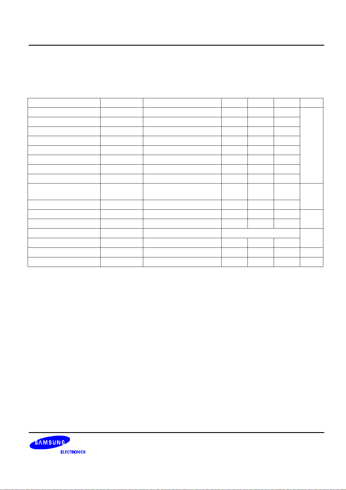
Parameter Symbol Condition Min. Typ. Max. Unit
Clock pulse width PWCLK - 18 - -
Clock pulse low period PWCLK (L) - 4 - -
Clock pulse high period PWCLK (H) - 4 - -
Data setup time tSETUP1 - 4 - -
Data hold time tHOLD1 - 0 - -
Start pulse setup time tSETUP2 - 4 - -
Start pulse hold time tHOLD2 - 0 - -
Start pulse delay time tPLH1 CL = 20pF - - 12
CLK1 – DIO (input)
setup time
CLK1 pulse high period PWCLK1 - 3 - Driver output delay time1
Driver output delay time2
Data invalid period tINV
Last data timing tLDT - 1 - -
CLK1 - CLK2 time tCLK1 - CLK2
POL - CLK1 time tPOL - CLK1
NOTES:
1. The value is specified when the drive voltage value reaches the target output voltage level of 90%
2. The value is specified when the drive voltage value reaches the target output voltage level of 6-bit accuracy.
tSETUP3 - 1 - -
(1)
tPHL1
tPHL2
(2)
Refer to Figure 5 - - 5
Refer to Figure 5 - - 10
DIO1 (2)↑ → CLK2↑
CLK1↑ → CLK2↑
POL↑or↓ → CLK1↑
6 - - ns
-9 - - ns
1
ns
CLK2
period
µs
CLK2
period
17
Page 18
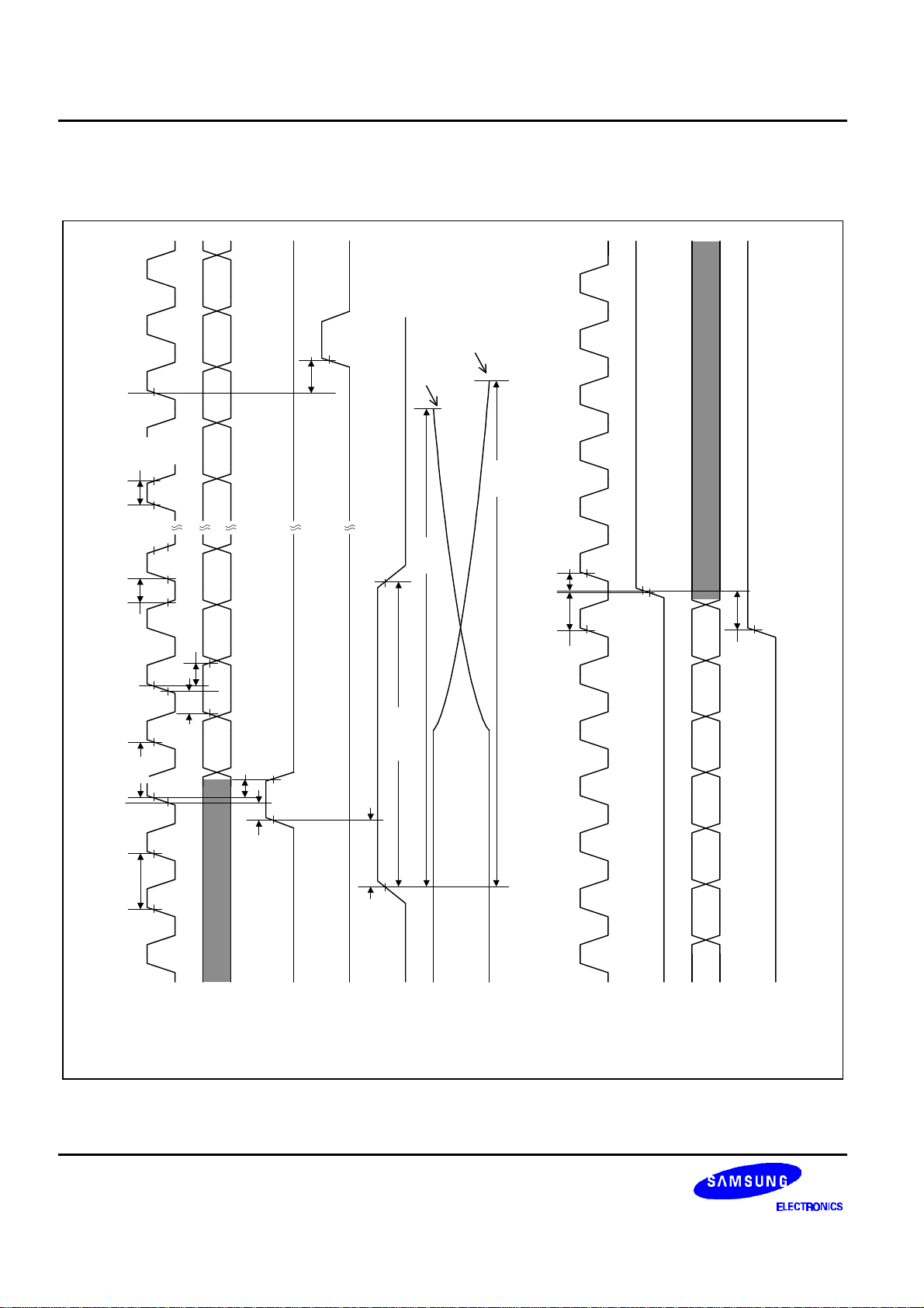
S6C1652 6 BIT 300 / 309 CHANNEL TFT-LCD SOURCE DRIVER
INVALID DATA
(DIO2 input)
DIO2 output
(DIO1 output)
tPOL - CLK1
WAVEFORMS (VIH = 0.75VDD1, VIL = 0.25VDD1)
PWCLK (H)
VIL
VIH
PWCLK (L)
1st LAST-1 LAST
tINV
tSETUP1
tHOLD1
1st
DATA
tHOLD2
tPLH1
Target output voltage
Target output voltage 90%
tPHL1
PWCLK1
tPHL2
tCLK1 - CLK2
tLDT
0.5VDD1
LAST
DATA
tSETUP3
CLK1
Y(1:309)
CLK2
CLK1
PWCLK
CLK2
tSETUP2
INVALID DATA
DXX
DIO1 input
Figure 6. Waveforms
18
DXX
POL
Page 19
6 BIT 300 / 309 CHANNEL TFT-LCD SOURCE DRIVER S6C1652
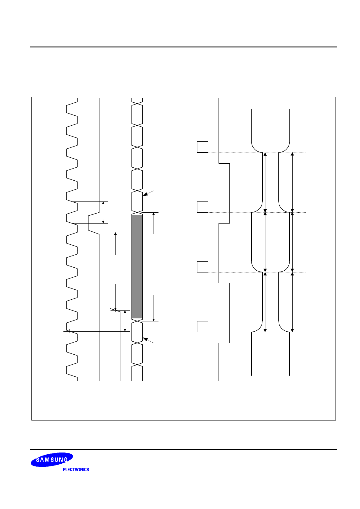
VGMA10 - VGMA18VGMA1 - VGMA9
number output
VGMA1 - VGMA9
VGMA10 - VGMA18VGMA10 - VGMA18
RELATIONSHIPS BETWEEN CLK1, START PULSE (DIO1, DIO2) AND
BLANKING PERIOD
2nd
DATA
First data in
the next line
1st
DATA
CLK2
1CLK2
0.5VDD1
DIO1 input
(DIO2 input)
1CLK2 (Min.)
CLK1
INVALID DATA
tLDT
Nth
N-1th
DXX
blanking time = Min. 3CLK2
DATA
DATA
Last data
Figure 7. Waveforms
CLK1
POL
VGMA1 - VGMA9
Y2N-1: odd
number output
Y2N: even
19
 Loading...