

Page 1
34COM/120SEG DRIVER & CONTROLLER FOR DOT MATRIX LCD S6A0079
INTRODUCTION
S6A0079 is a dot matrix LCD driver & controller LSI which is fabricated by low power CMOS technology. It can
display 2, or 4 lines with 5 x 8 dots format.
FUNCTIONS
• Character type dot matrix LCD driver & controller
• Internal driver: 34 common and 120 segment signal output
• Easy interface with 4-bit or 8-bit MPU
• 5 x 8 dots matrix possible
• Voltage converter for LCD drive voltage: 13V max (2 times/3 times)
• Automatic power on reset
FEATURES
• Internal memory
- Character Generator ROM (CGROM): 9,600 bits (240 characters x 5 x 8 dot)
- Character Generator RAM (CGRAM): 64 x 8 bits (8 characters x 5 x 8 dot)
- Icon RAM (CGRAM): 16 x 8 bits (80 icons max.)
- Display Data RAM (DDRAM): 96 x 8 bits (96 characters max.)
• Low power operation
- Power supply voltage range: 2.7 - 5.5V (VDD)
- LCD Drive voltage range: 3.0 - 13.0V (VDD - V5)
• CMOS process
• Duty cycle: 1/33
• Internal oscillator with an external resistor
• Bare chip available
PROGRAMMABLE DUTY CYCLES
5-Dot Font Width
Display Line Duty Ratio Single-chip Operation
Numbers
2 1/33 2-line of 48 characters 80
Displayable Characters Possible Icons
4 1/33 4-line of 24 characters 80
1
Page 2
S6A0079 34COM/120SEG DRIVER & CONTROLLER FOR DOT MATRIX LCD
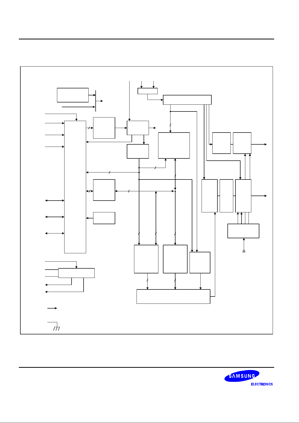
BLOCK DIAGRAM
OSC1 OSC2TEST1
RESET
TEST2
RS
RW
DB4-DB7
DB3-DB1
DB0
Power on Reset
(POR)
Instruction
8
System
E
Interface
4-bit
8-bit
Input/
Output
Buffer
Register
(IR)
7
Data
8 8
Register
(DR)
Busy Flag
Oscillator
Instruction
Decoder
Address
Counter
7 8
Display Data
RAM (DDRAM)
96 x 8-bit
7
Timing Generator
7
8
8
120-bit
Shift
Register
34-bit
Shift
Register
120-bit
Latch
Circuit
Common
Driver
Segment
Driver
LCD Driver
Voltage Selector
COM0COM33
SEG1SEG120
Vci
C1
C2
V5OUT2
V5OUT3
VDD
GND(VSS)
Character
Generator
RAM
(CGRAM)
64 bytes
Voltage Converter
Parallel/Serial Converter and
Character
Generator
ROM
(CGROM)
9600 bits
55
Smooth Scroll Circuit
Cursor and
Blink
Controller
V1 - V5
2
Page 3
34COM/120SEG DRIVER & CONTROLLER FOR DOT MATRIX LCD S6A0079
V5OUT2
V5OUT3
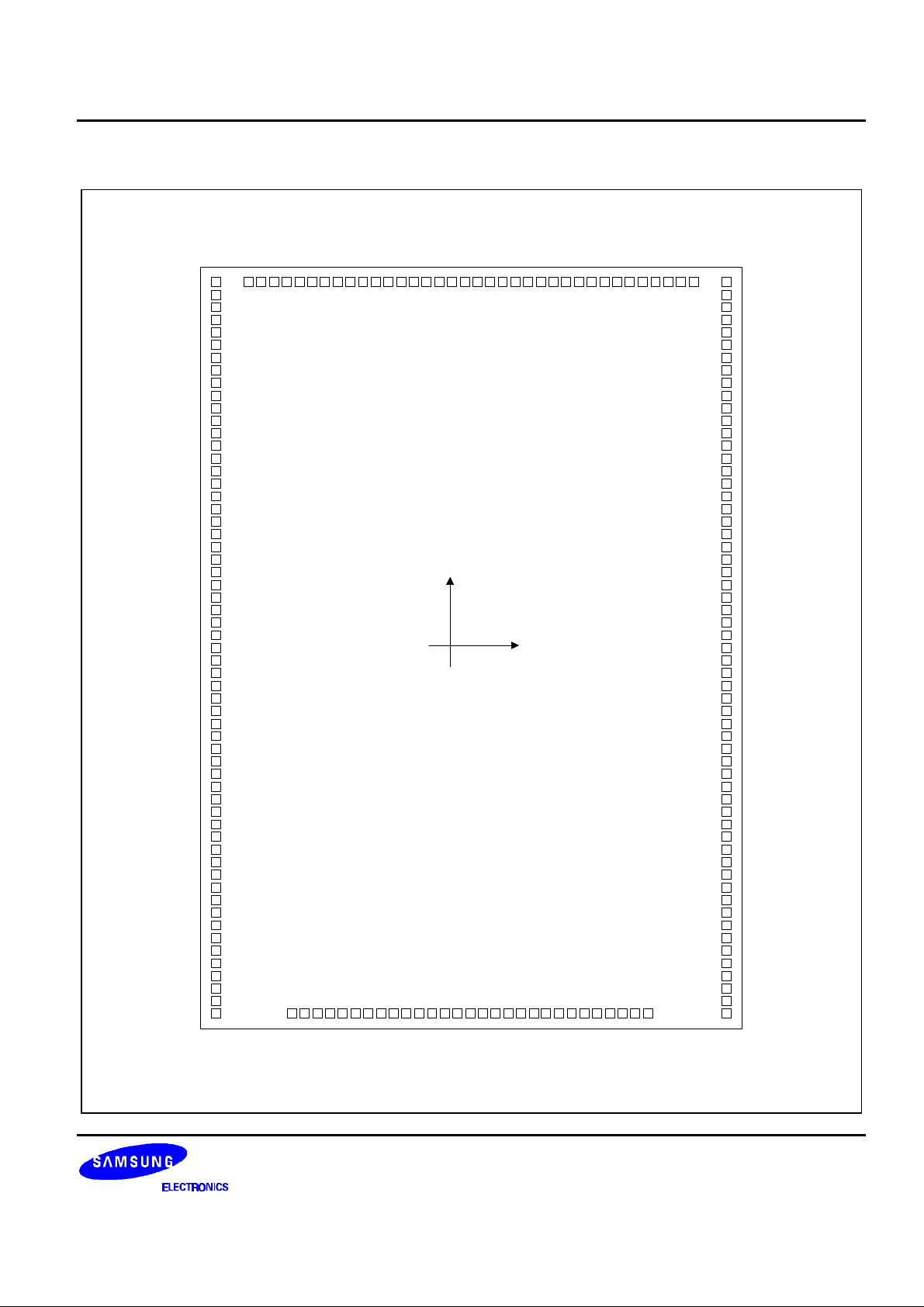
PAD CONFIGURATION
SEG43
SEG44
SEG45
SEG46
SEG47
SEG48
SEG49
SEG50
SEG51
SEG52
SEG53
SEG54
SEG55
SEG56
SEG57
SEG58
SEG59
SEG60
SEG61
SEG62
SEG63
SEG64
SEG65
SEG66
SEG67
SEG68
SEG69
SEG70
SEG71
SEG72
SEG73
SEG74
SEG75
SEG76
SEG77
SEG78
183
182
181
180
179
178
177
176
175
174
173
172
171
170
169
168
167
166
165
164
163
162
161
160
159
158
157
156
155
154
153
152
151
150
149
148
SEG42
SEG41
SEG40
SEG39
SEG38
SEG37
SEG36
SEG35
SEG34
SEG33
SEG32
SEG31
SEG30
SEG29
SEG28
SEG27
SEG26
SEG25
SEG24
SEG23
SEG22
SEG21
SEG20
SEG19
SEG18
SEG17
SEG16
SEG15
SEG14
SEG13
SEG12
SEG11
SEG10
SEG9
SEG8
SEG7
SEG6
SEG5
SEG4
SEG3
SEG2
SEG1
COM9
COM10
COM11
COM12
COM13
COM14
COM15
COM16
COM25
COM26
COM27
COM28
COM29
COM30
COM31
COM32
COM33
1
2
3
4
5
6
7
8
9
10
11
12
13
14
15
16
17
18
19
20
21
22
23
24
25
26
27
28
29
30
31
32
33
34
35
36
37
38
39
40
41
42
43
44
45
46
47
48
49
50
51
52
53
54
55
56
57
58
59
Y
(0, 0) X
Chip size: 5340
PAD size: 100
Unit : µm
×
8740
×
100
147
146
145
144
143
142
141
140
139
138
137
136
135
134
133
132
131
130
129
128
127
126
125
124
123
122
121
120
119
118
117
116
115
114
113
112
111
110
109
108
107
106
105
104
103
102
101
100
99
98
97
96
95
94
93
92
91
90
89
SEG79
SEG80
SEG81
SEG82
SEG83
SEG84
SEG85
SEG86
SEG87
SEG88
SEG89
SEG90
SEG91
SEG92
SEG93
SEG94
SEG95
SEG96
SEG97
SEG98
SEG99
SEG100
SEG101
SEG102
SEG103
SEG104
SEG105
SEG106
SEG107
SEG108
SEG109
SEG110
SEG111
SEG112
SEG113
SEG114
SEG115
SEG116
SEG117
SEG118
SEG119
SEG120
COM0
COM1
COM2
COM3
COM4
COM5
COM6
COM7
COM8
COM17
COM18
COM19
COM20
COM21
COM22
COM23
COM24
6061626364656667686970717273747576777879808182838485868788
VDD
OSC2
OSC1
TEST2
RESET
SS1
V
TEST1
RS
RW
E
DB0
DB1
DB2
DB3
DB4
DB5
DB6
DB7
Vci
C2
C1
VSS2
V5V4V3V2V1
3
Page 4
S6A0079 34COM/120SEG DRIVER & CONTROLLER FOR DOT MATRIX LCD
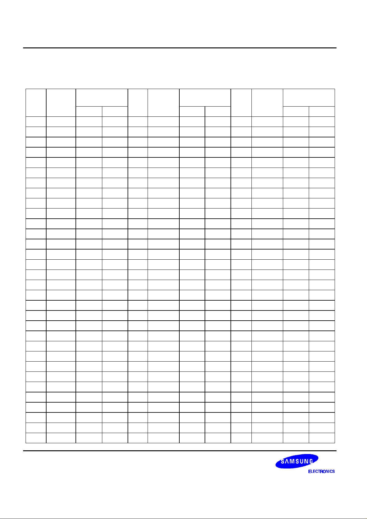
PAD CENTER COORDINATES
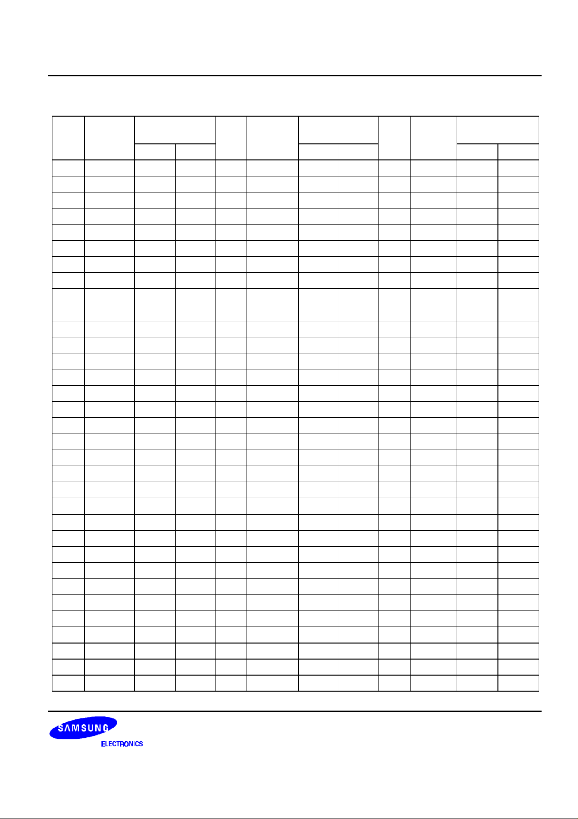
Table 1. Pad Location
Pad
No.
X Y X Y X Y
1 SEG42 -2504 3540 33 SEG10 -2504 -459 65 TESET1 -1125 -4119
2 SEG41 -2504 3415 34 SEG9 -2504 -584 66 VSSI -1000 -4119
3 SEG40 -2504 3290 35 SEG8 -2504 -709 67 RS -875 -4119
4 SEG39 -2504 3165 36 SEG7 -2504 -834 68 RW -750 -4119
5 SEG38 -2504 3040 37 SEG6 -2504 -959 69 E -625 -4119
6 SEG37 -2504 2915 38 SEG5 -2504 -1084 70 DB0 -500 -4119
7 SEG36 -2504 2790 39 SEG4 -2504 -1209 71 DB1 -375 -4119
8 SEG35 -2504 2665 40 SEG3 -2504 -1334 72 DB2 -250 -4119
9 SEG34 -2504 2540 41 SEG2 -2504 -1459 73 DB3 -125 -4119
10 SEG33 -2504 2415 42 SEG1 -2504 -1584 74 DB4 0 -4119
11 SEG32 -2504 2290 43 COM9 -2504 -1822 75 DB5 125 -4119
12 SEG31 -2504 2165 44 COM10 -2504 -1947 76 DB6 250 -4119
13 SEG30 -2504 2040 45 COM11 -2504 -2072 77 DB7 375 -4119
14 SEG29 -2504 1915 46 COM12 -2504 -2197 78 Vci 500 -4119
15 SEG28 -2504 1790 47 COM13 -2504 -2322 79 C2 625 -4119
16 SEG27 -2504 1665 48 COM14 -2504 -2447 80 C1 750 -4119
17 SEG26 -2504 1540 49 COM15 -2504 -2572 81 VSS2 875 -4119
18 SEG25 -2504 1425 50 COM16 -2504 -2697 82 V5OUT2 1000 -4119
19 SEG24 -2504 1290 51 COM25 -2504 -2822 83 V5OUT3 1125 -4119
20 SEG23 -2504 1165 52 COM26 -2504 -2947 84 V5 1250 -4119
21 SEG22 -2504 1040 53 COM27 -2504 -3072 85 V4 1375 -4119
22 SEG21 -2504 915 54 COM28 -2504 -3197 86 V3 1500 -4119
23 SEG20 -2504 790 55 COM29 -2504 -3322 87 V2 1625 -4119
24 SEG19 -2504 665 56 COM30 -2504 -3447 88 V1 1750 -4119
25 SEG18 -2504 540 57 COM31 -2504 -3572 89 COM24 2504 -3822
26 SEG17 -2504 415 58 COM32 -2504 -3697 90 COM23 2504 -3697
27 SEG16 -2504 290 59 COM33 -2504 -3822 91 COM22 2504 -3572
28 SEG15 -2504 165 60 VDD -1750 -4119 92 COM21 2504 -3447
29 SEG14 -2504 40 61 OSC2 -1625 -4119 93 COM20 2504 -3322
30 SEG13 -2504 -84 62 OSC1 -1500 -4119 94 COM19 2504 -3197
31 SEG12 -2504 -209 63 RESET -1375 -4119 95 COM18 2504 -3072
32 SEG11 -2504 -334 64 TEST2 -1250 -4119 96 COM17 2504 -2947
Pad
Name
Coordinate Pad
No.
Pad
Name
Coordinate Pad
No.
Pad
Name
Coordinate
4
Page 5
34COM/120SEG DRIVER & CONTROLLER FOR DOT MATRIX LCD S6A0079
Table 1. Pad Location (Continued)
Pad
Pad Name
No.
X Y X Y X Y
97 COM8 2504 -2822 130
98 COM7 2504 -2697 131
99 COM6 2504 -2572 132
100
101
102
103
104
105
106 SEG120 2504 -1584 139
107 SEG119 2504 -1459 140
108 SEG118 2504 -1334 141
109 SEG117 2504 -1209 142
110 SEG116 2504 -1084 143
111 SEG115 2504 -959 144
112 SEG114 2504 -834 145
113 SEG113 2504 -709 146
114 SEG112 2504 -584 147
115 SEG111 2504 -459 148
116 SEG110 2504 -334 149
117 SEG109 2504 -209 150
118 SEG108 2504 -84 151
119 SEG107 2504 40 152
120 SEG106 2504 165 153
121 SEG105 2504 290 154
122 SEG104 2504 415 155
123 SEG103 2504 540 156
124 SEG102 2504 665 157
125 SEG101 2504 790 158
126 SEG100 2504 915 159
127 SEG99 2504 1040 160
128 SEG98 2504 1165 161
129 SEG97 2504 1290 162
COM5 2504 -2447 133
COM4 2504 -2322 134
COM3 2504 -2197 135
COM2 2504 -2072 136
COM1 2504 -1947 137
COM0 2504 -1822 138
Coordinate Pad
No.
Pad
Name
SEG96 2504 1415 163 SEG63 312 4119
SEG95 2504 1540 164 SEG62 187 4119
SEG94 2504 1665 165 SEG61 62 4119
SEG93 2504 1790 166 SEG60 -62 4119
SEG92 2504 1915 167 SEG59 -187 4119
SEG91 2504 2040 168 SEG58 -312 4119
SEG90 2504 2165 169 SEG57 -437 4119
SEG89 2504 2290 170 SEG56 -562 4119
SEG88 2504 2415 171 SEG55 -687 4119
SEG87 2504 2540 172 SEG54 -812 4119
SEG86 2504 2665 173 SEG53 -937 4119
SEG85 2504 2790 174 SEG52 -1062 4119
SEG84 2504 2915 175 SEG51 -1187 4119
SEG83 2504 3040 176 SEG50 -1312 4119
SEG82 2504 3165 177 SEG49 -1437 4119
SEG81 2504 3290 178 SEG48 -1562 4119
SEG80 2504 3415 179 SEG47 -1687 4119
SEG79 2504 3540 180 SEG46 -1812 4119
SEG78 2187 4119 181 SEG45 -1937 4119
SEG77 2062 4119 182 SEG44 -2062 4119
SEG76 1937 4119 183 SEG43 -2187 4119
SEG75 1812 4119
SEG74 1687 4119
SEG73 1562 4119
SEG72 1437 4119
SEG71 1312 4119
SEG70 1187 4119
SEG69 1062 4119
SEG68 937 4119
SEG67 812 4119
SEG66 687 4119
SEG65 562 4119
SEG64 437 4119
Coordinate Pad
No.
Pad
Name
Coordinate
5
Page 6
S6A0079 34COM/120SEG DRIVER & CONTROLLER FOR DOT MATRIX LCD
PAD DESCRIPTION
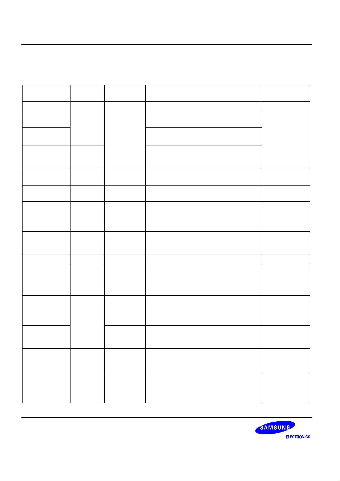
Table 2. Pad Description
Pad (No) Input/
Name Description Interface
Output
VDD (60) Power supply For logical circuit (+3V, +5V) Power supply
VSS1, VSS2
- 0V (GND)
(66, 81)
V1-V5
(88-84)
Vci (78) Input Input voltage to the voltage converter to
Bias voltage level for LCD driving
generate LCD drive voltage
(Vci = 1.0 - 4.5V).
SEG1-SEG120
(1-42, 106-183)
COM0-COM33
(105-89, 43-59)
OSC1, OSC2
(61, 62)
C1,C2
(80, 79)
Output Segment
output
Output Common
output
Input
Oscillator When use internal oscillator, connect
(OSC1),
Output
(OSC2)
Input External
capacitance
input
Segment signal output for LCD drive LCD
Common signal output for LCD drive LCD
External
external Rf resistor.
If external clock is used, connect it to
resistor/oscillator
(OSC1)
OSC1.
To use the voltage converter (2 times /3
times), these pins must be connected to the
External
capacitance
external capacitance.
RESET (63) Input Reset pin Initialized to low TEST1 (65) Input Test pin When TEST1 = "High", Test mode
When TEST1 = "Low", Normal operation
mode
This pin must be set to VSS
V5OUT2 (82) Output Two times
converter
output
The value of Vci is converted two times.
To use three times converter, the same
capacitance as that of C1-C2 should be
V5 capacitance
connected here.
V5OUT3 (83) Three times
The value of Vci is converted three times. V5
converter
output
TEST2 (64) Input Test pin When TEST2 = "High" : Normal mode
When TEST2 = "Low": Test mode
This pin must be set to VDD
RS (67) Input Register
select
Register selection input
In RS = "High", Data register is selected.
In RS = "Low", Instruction register is
MPU
selected.
6
Page 7
34COM/120SEG DRIVER & CONTROLLER FOR DOT MATRIX LCD S6A0079
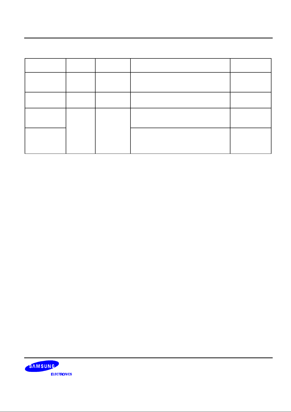
Table 2. Pad Description (Continued)
Pad (No) Input/
Name Description Interface
Output
RW (68) Input Read/write Read/write selection input.
In RW= "High", read operation.
When RW = "Low", write operation.
E (69) Input Read/write
enable
DB0-DB3
(70-73)
Input.
Output
Data bus 0-7 In 8-bit bus mode, used as low order bi-
Read/write enable signal.
directional data bus.
During 4-bit bus mode, open these pins.
DB4-DB7
(74-77)
In 8-bit bus mode, used as high order bi-
directional data bus. In case of 4-bit bus
mode, used as both high and low order.
DB7 used for busy flag output.
MPU
MPU
MPU
MPU
7
Page 8
S6A0079 34COM/120SEG DRIVER & CONTROLLER FOR DOT MATRIX LCD
FUNCTION DESCRIPTION
SYSTEM INTERFACE
This chip has all two kinds interface type with MPU: 4-bit bus and 8-bit bus. 4-bit bus and 8-bit bus is selected by
DL bit in the instruction register. During read or write operation, two 8-bit registers are used. one is data register
(DR), the other is instruction register(IR).
The data register(DR) is used as temporary data storage place for being written into or read from
DDRAM/CGRAM target RAM is selected by RAM address setting instruction. Each internal operation, reading
from or writing into RAM, is done automatically.
Hence, after MPU reads DR data, the data in the next DDRAM/CGRAM address is transferred into DR
automatically. Also after MPU writes data to DR, the data in DR is transferred into DDRAM/CGRAM
automatically.
The Instruction register(IR) is used only to store instruction code transferred from MPU. MPU cannot use it to
read instruction data.
To select register, use RS input pin in 4-bit/8-bit bus mode.
RS R/W Operation
0 0 Instruction write operation (MPU writes instruction code into IR)
0 1 Read busy flag (DB7) and address counter (DB0 - DB6)
1 0 Data write operation (MPU writes data into DR)
1 1 Data read operation (MPU reads data from DR)
BUSY FLAG (BF)
When BF = "High", it indicates that the internal operation is being processed. So during this time the next
instruction cannot be accepted. BF can be read, when RS = Low and R/W = High (Read Instruction Operation),
through DB7 port. Before executing the next instruction, be sure that BF is not high.
8
Page 9
34COM/120SEG DRIVER & CONTROLLER FOR DOT MATRIX LCD S6A0079
DISPLAY DATA RAM (DDRAM)
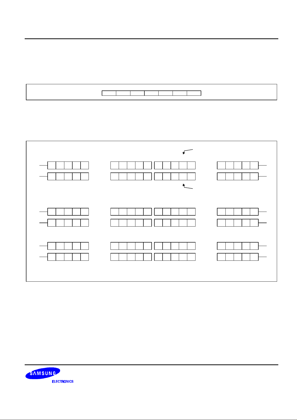
DDRAM stores display data of maximum 96 x 8 bits (96 characters). DDRAM address is set in the address
counter (AC) as a hexadecimal number. (refer to Figure 1.)
MSB LSB
AC6 AC5 AC4 AC3 AC2 AC1 AC0
Figure 1. DDRAM Address
5-dot 2-line Display
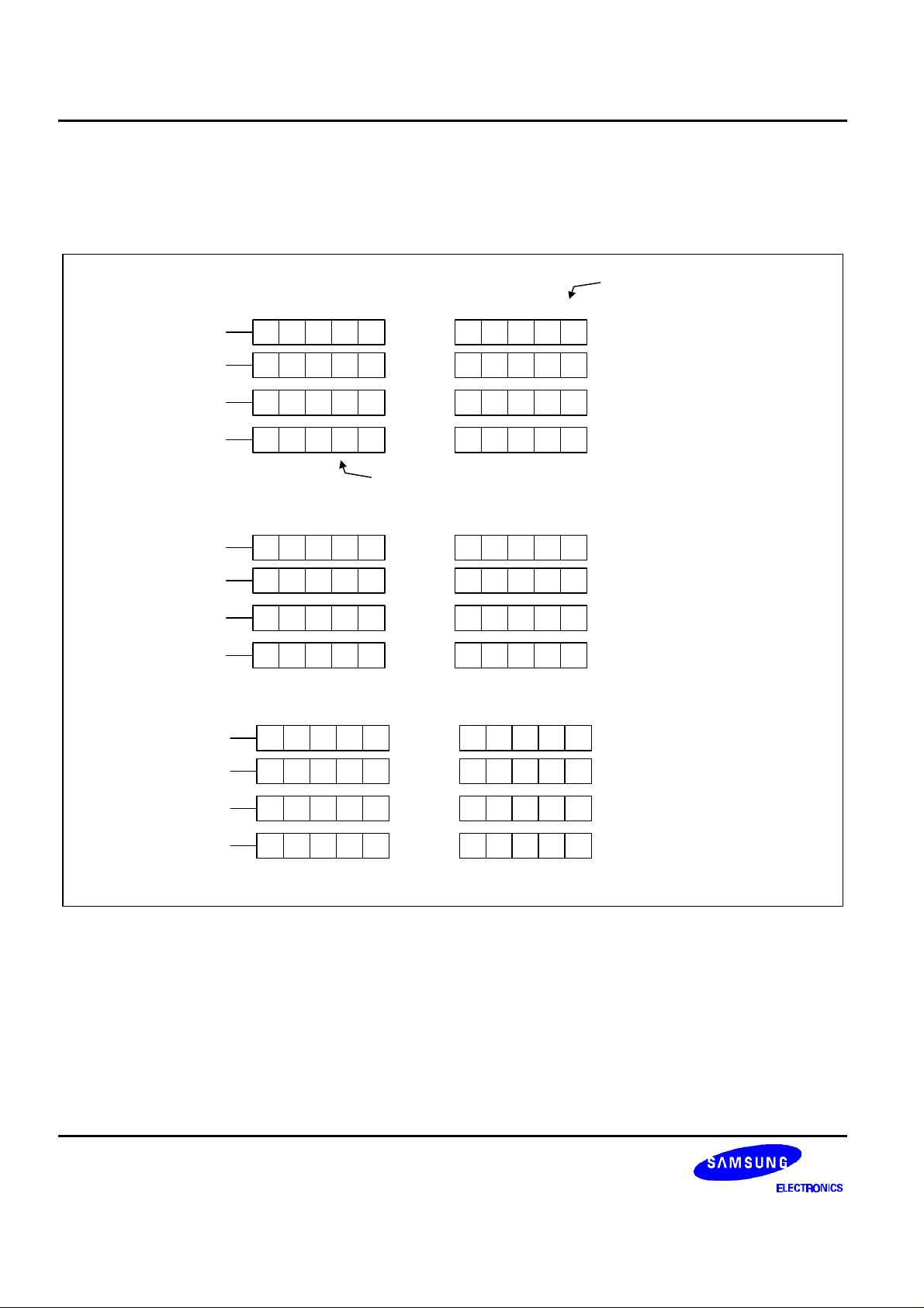
In case of 2-line display with 5-dot font, the address range of DDRAM is 00H-2FH, 40H-6FH. (refer to Figure 2)
Display Position
COM1
COM8
COM17
COM24
COM1
COM8
COM17
COM24
COM1
COM8
COM17
COM24
1 2 3 4 5
00 01 02 03 04
40 41 42 43 44
SEG1
1 2 3 4 5
41 42 43 44
1 2 3 4 5
00 01 02 032F
6F 40 41 42
20 21 22 23 24
. . . . 13 14 15 16 17
. . . . 53 54 55 56 57 58 59 5A 5B 5C . . . . 6B 6C 6D 6E 6F
SEG120
S6A0079 S6A0079
20 21 22 23 24
0501 02 03 04
. . . . 14 15 16 17
. . . . 54 55 56 57 58 59 5A 5B 5C . . . . 6C 6D 6E 6F
45 5D 40
(After Shift Left)
20 21 22 23 24
. . . . 13 14 15 16 17
. . . . 52 53 54 55 56 57 58 59 5A . . . . 6A 6B 6C 6D
43 5B 6E
12
(After Shift Right)
25 26 27 28 29
18 19 1A 1B 1C
SEG1
25 26 27 28 29
19 1A 1B 1C
18 1D
25 26 27 28 29
18 19 1A 1B
44 45 46 47 48
. . . . 2B 2C 2D 2E 2F
SEG120
DDRAM Address
44 45 46 47 48
. . . . 2C 2D 2E 2F 00
44 45 46 47 48
. . . . 2A 2B 2C 2D 2E
Figure 2. 2-line X 48ch. Display (5-dot Font Width)
COM9
COM16
COM25
COM32
COM9
COM16
COM25
COM32
COM9
COM16
COM25
COM32
9
Page 10
S6A0079 34COM/120SEG DRIVER & CONTROLLER FOR DOT MATRIX LCD
5-dot 4-line Display
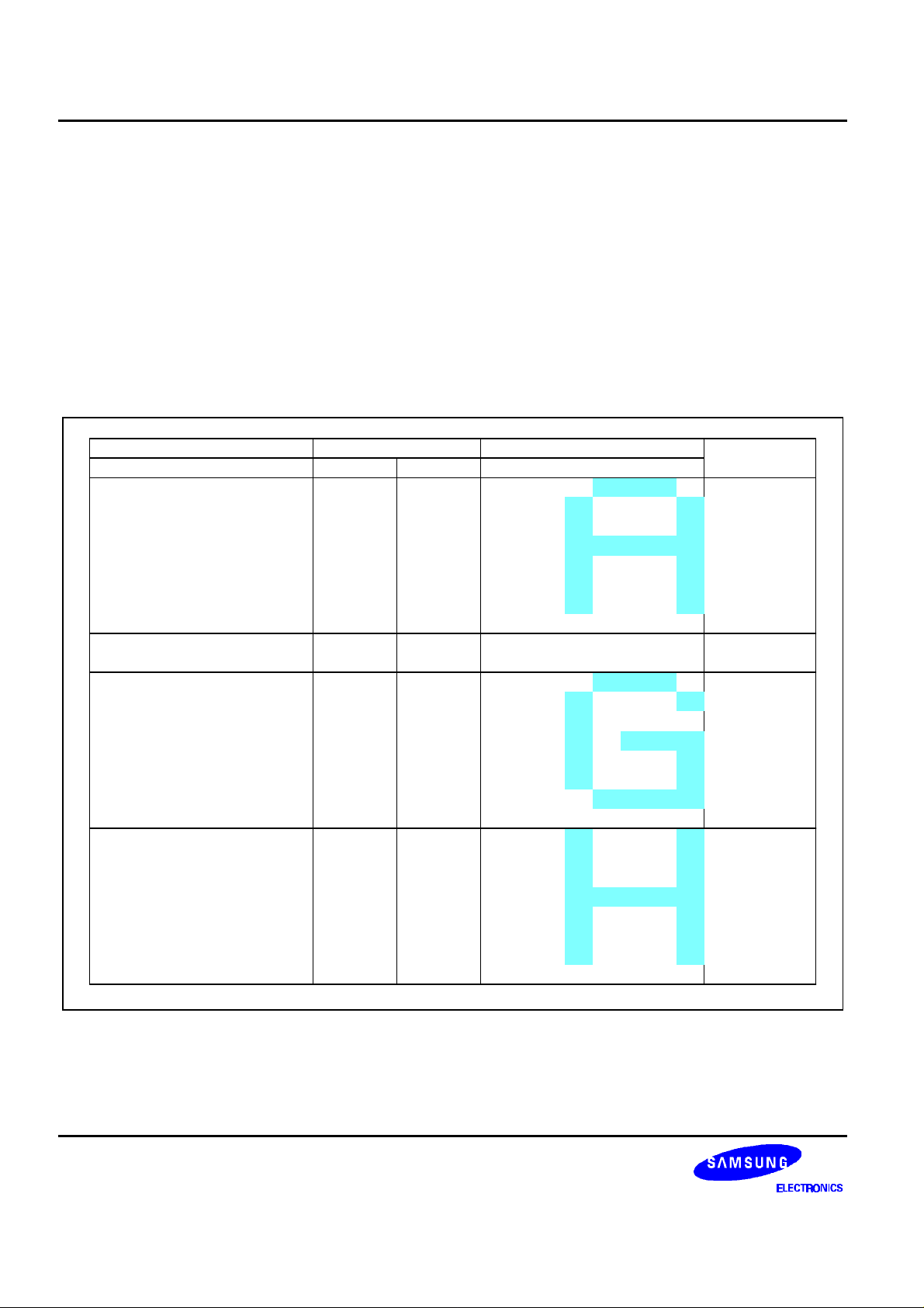
In case of 4-line display with 5-dot font, the address range of DDRAM is 00H-17H, 20H-37H, 40H-57H, 60H-77H.
(refer to Figure 3)
Display Position
COM1
COM8
COM9
COM16
COM17
COM24
COM25
COM32
COM1
COM8
COM9
COM16
COM17
COM24
COM25
COM32
COM1
COM8
COM9
COM16
COM17
COM24
COM25
COM32
1 2 3 4 5
00 01 02 03 04
61 62 63 6460
SEG1
1 2 3 4 5
01 02 03 04
2421 22 23
4441 42 43
61 62 63 64
1 2 3 4 5
00 01 02 03
17
20 21 22 23
37
40 41 42 43
57
77
61 62 6360
20 21 22 23 24
. . . . 13 14 15 16 17
2420 21 22 23
. . . . 33 34 35 36 37
4440 41 42 43
. . . . 53 54 55 56
. . . . 74 75 76 7773
DDRAM Address
S6A0079
20 21 22 23 24
. . . . 14 15 16 17
05
. . . . 34 35 36 37
25
. . . . 54 55 56
45
. . . . 74 75 76 77
65
(After Shift Left)
20 21 22 23 24
. . . . 13 14 15 1612
. . . . 33 34 35 3632
. . . . 53 54 55 56
. . . . 74 75 7672 73
(After Shift Right)
52
57
SEG120
00
20
57
40
60
Figure 3. 4-line X 24ch. Display (5-dot Font Width)
10
Page 11

34COM/120SEG DRIVER & CONTROLLER FOR DOT MATRIX LCD S6A0079
TIMING GENERATION CIRCUIT
Timing generation circuit generates clock signals for the internal operations.
ADDRESS COUNTER (AC)
Address Counter (AC) stores DDRAM/CGRAM address, transferred from IR. After writing into (reading from)
DDRAM/CGRAM, AC is automatically increased (decreased) by 1. When RS = "Low" and R/W = "High", AC can
be read through DB0 - DB6.
CURSOR/BLINK CONTROL CIRCUIT
It controls cursor/blink ON/OFF and black/white inversion at cursor position.
LCD DRIVER CIRCUIT
LCD Driver circuit has 34 common and 120 segment signals for LCD driving. Data from CGRAM/CGROM is
transferred to 120-bit segment latch serially, which is stored to 120-bit shift latch. When each common is selected
by 34-bit common register, segment data also output through segment driver from 120-bit segment latch. In case
of 2-line or 4-line mode, COM0-COM33 have 1/33 duty ratio. COM0 (COM33) makes the data of CGRAM (Icon
RAM) enable to display icons.
11
Page 12
S6A0079 34COM/120SEG DRIVER & CONTROLLER FOR DOT MATRIX LCD
CGROM (CHARACTER GENERATOR ROM)
CGROM has 5 X 8 dots 240 characters pattern.
CGRAM (Character Generator RAM)
5 x 8 Dot Character Pattern
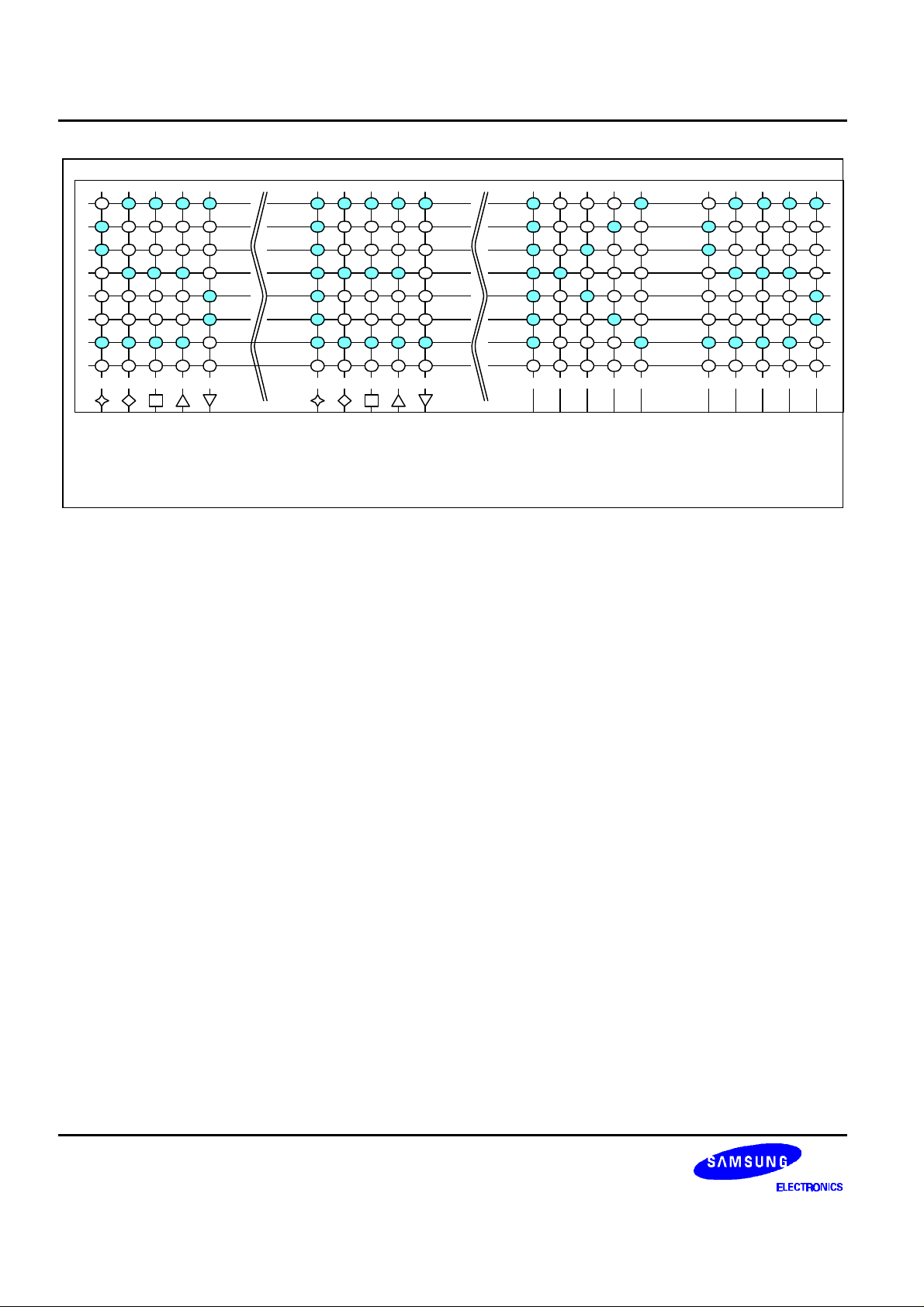
By writing font data to CGRAM, user defined character can be used. (refer to Table 4) pattern 7 and pattern 8 to
CGRAM can be used in common by CGRAM and IconRAM. But CGRAM and IconRAM is used exclusively to
pattern 7 or pattern 8 of CGRAM. CGRAM has up to 5 X 8-dot 6 - 8 characters.
Table 4. Relationship between Character Code (DDRAM) and Character Pattern (CGRAM)
Character Code (DDRAM data) CGRAM Address CGRAM Data
D7 D6 D5 D4 D3 D2 D1 D0 A5 A4 A3 A2 A1 A0 P7 P6 P5 P4 P3 P2 P1 P0
0 0 x0 0 0 0 0 0 0 0 0 0
0 0
0 0
.
.
.
.
.
.
.
0 0 0 x0 1 1 0 1 1 0 0 0 0
.
.
.
.
.
.
.
.
.
.
.
.
.
.
.
.
.
.
.
.
.
.
.
.
.
.
.
1
0
1 1
0 0
1
0
1 1
1 1
1 1 1
.
.
0 0
0 0
1
0
1 1
0 0
1
0
1 1
1 1
1 1 1
0 0
0 0
1
0
1 1
0 0
1
0
1 1
1 1
1 1 1
x x x 0 0
1
.
.
.
.
.
0
x x x
1
.
.
.
.
.
0
x x x
1
.
.
.
.
.
0
1 1 10
1
0 0 0
1
0 0 0
1
1 1 1 1
1
0 0 0
1
0 0 0
1
0 0 0
0
0 0 0 0
.
.
10 01 1
1
0 0 0
1
0 0 0
1
0 1 1 1
1
0 0 0
1
0 0 0
0
1 1 1
0
0 0 0 0
01 10 00 0 0 x0 1 1 1 1 1 1 0 0 0
1
0 0 0
1
0 0 0
1
1 1 1 1
1
0 0 0
1
0 0 0
1
0 0 0
0
0 0 0 0
Pattern
Number
Pattern 1
1
1
1
1
1
.
.
Pattern 7
1
0
1
1
1
Pattern 8
1
1
1
1
1
12
Page 13

34COM/120SEG DRIVER & CONTROLLER FOR DOT MATRIX LCD S6A0079
CGRAM (ICON RAM)
CGRAM (Icon RAM) has segment control data and segment pattern data. COM0 (COM33) makes the data of
CGRAM(Icon RAM) enable to display icons. Its lower 5-bit are pattern data. (refer to Table 5 and Figure 4)
Table 5. Relationship Between CGRAM (Icon RAM) Address and Display Pattern
CGRAM Address CGRAM Data Display Pattern
5-Dot Font Width
A5 A4 A3 A2 A1 A0 D7 D6 D5 D4 D3 D2 D1 D0
1 1 0 0 0 0 X X X S76 S77 S78 S79 S80 CGRAM pattern 7
1 1 0 0 0 1 X X X S71 S72 S73 S74 S75
1 1 0 0 1 0 X X X S66 S67 S68 S69 S70
1 1 0 0 1 1 X X X S61 S62 S63 S64 S65
1 1 0 1 0 0 X X X S56 S57 S58 S59 S60
1 1 0 1 0 1 X X X S51 S52 S53 S54 S55
1 1 0 1 1 0 X X X S46 S47 S48 S49 S50
1 1 0 1 1 1 X X X S41 S42 S43 S44 S45
1 1 1 0 0 0 X X X S36 S37 S38 S39 S40 CGRAM pattern 8
1 1 1 0 0 1 X X X S31 S32 S33 S34 S35
1 1 1 0 1 0 X X X S26 S27 S28 S29 S30
1 1 1 0 1 1 X X X S21 S22 S23 S24 S25
1 1 1 1 0 0 X X X S16 S17 S18 S19 S20
1 1 1 1 0 1 X X X S11 S12 S13 S14 S15
1 1 1 1 1 0 X X X S6 S7 S8 S9 S10
1 1 1 1 1 1 X X X S1 S2 S3 S4 S5
Note: 1. S1 - S80: Icon pattern ON/OFF in 5-dot font width.
2. "X": Don't care
13
Page 14
S6A0079 34COM/120SEG DRIVER & CONTROLLER FOR DOT MATRIX LCD
SEG76
SEG77
SEG78
SEG79
SEG80
SEG111
SEG112
SEG113
SEG114
SEG115
SEG116
SEG117
SEG118
SEG119
SEG120
S1 S2 S3 S4 S5 S76 S77 S78 S79 S80
SEG1
SEG2
SEG3
SEG4
SEG5
Figure 4. Relationship between CGRAM (Icon RAM) and Segment Display
S111S112S113S114 S115 S116 S117 S118 S119S120
. . .. . .
14
Page 15

34COM/120SEG DRIVER & CONTROLLER FOR DOT MATRIX LCD S6A0079
INSTRUCTION DESCRIPTION
OUTLINE
To overcome the speed difference between internal clock of S6A0079 and MPU clock, S6A0079 performs
internal operation by storing control information to IR or DR. The internal operation is determined according to the
signal from MPU, composed of read/write and data bus. (refer to Table 6) Instruction can be divided largely four
kinds,
• S6A0079 function set instructions (set display methods, set data length, etc.)
• Address set instructions to internal RAM
• Data transfer instructions with internal RAM
• Others.
The address of internal RAM is automatically increased or decreased by 1.
NOTE: During internal operation, Busy Flag (DB7) is read High. Busy Flag check must precede the next instruction. When
you make a MPU program with checking the Busy Flag (DB7), it must be necessary 1/2 fosc for executing the next
instruction by falling E signal after the Busy Flag (DB7) goes to "Low".
15
Page 16
S6A0079 34COM/120SEG DRIVER & CONTROLLER FOR DOT MATRIX LCD
Assign cursor moving direction.
INSTRUCTION DESCRIPTION
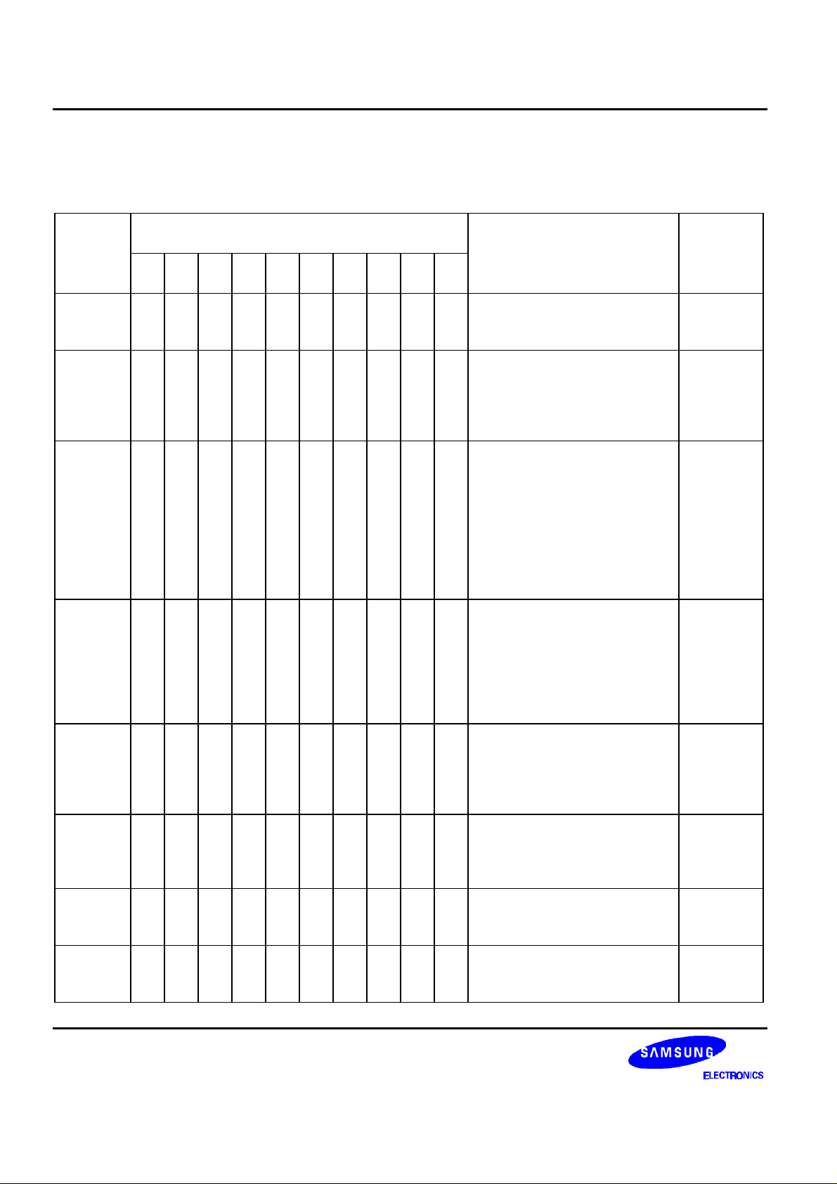
Table 6. Instruction Set
Instruction
RS R/W DB7 DB6 DB5 DB4 DB3 DB2 DB1 DB0
Clear
0 0 0 0 0 0 0 0 0 1 Write "20H" to DDRAM. and
display
Return
home
Entry
mode set
0 0 0 0 0 0 0 0 1 X
0 0 0 0 0 0 0 1 I/D S
Display
on/off
control
Cursor or
display
shift
Function
set
Set
CGRAM
address
Set
DDRAM
address
0 0 0 0 0 0 1 D C B
0 0 0 0 0 1 S/C R/L X X
0 0 0 0 1 DL N X X X
0 0 0 1 AC5 AC4 AC3 AC2 AC1 AC0 Set CGRAM address in address
0 0 1 AC6 AC5 AC4 AC3 AC2 AC1 AC0 Set DDRAM address in address
Instruction Code Description Execution
Time
(fosc =
270kHz)
1.53ms
set DDRAM address to "00H"
from AC.
Set DDRAM address to "00H"
1.53ms
from AC and return cursor to its
original position if shifted. The
contents of DDRAM are not
changed.
39µs
I/D = "1": increment,
I/D = "0": decrement and
display shift enable
bit.
S = "1": make entire display
shift of all lines during
DDRAM write.
S = "0": display shift disable
Set display/cursor/blink on/off
39µs
D = "1": display on,
D = "0": display off,
C = "1": cursor on,
C = "0": cursor off,
B = "1": blink on,
B = "0": blink off.
Cursor or display shift.
39µs
S/C = "1": display shift,
S/C = "0": cursor shift,
R/L = "1": shift to right,
R/L = "0": shift to left.
Set interface data length
39µs
(DL = "1": 8-bit, DL = "0": 4-bit),
numbers of display line when
(N = "1": 4-line, N = "0": 2-line).
39µs
counter.
39µs
counter.
16
Page 17
34COM/120SEG DRIVER & CONTROLLER FOR DOT MATRIX LCD S6A0079
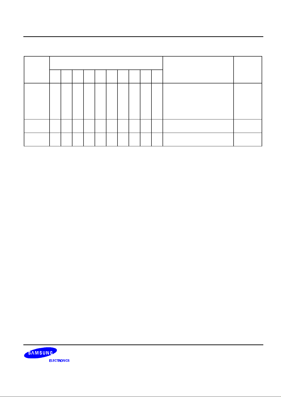
address counter can also be read.
Table 6. Instruction Set (Continued)
Instruction
RS R/W DB7 DB6 DB5 DB4 DB3 DB2 DB1 DB0
Read busy
flag and
address
Write data 1 0 D7 D6 D5 D4 D3 D2 D1 D0 Write data into internal RAM
Read data 1 1 D7 D6 D5 D4 D3 D2 D1 D0 Read data from internal RAM
NOTES:
1. When an MPU program with busy flag (DB7) checking is made, 1/2 fosc is necessary for executing the next instruction
by the "E" signal after the busy flag (DB7) goes to "Low".
2. "X": Don’t care.
0 1 BF AC6 AC5 AC4 AC3 AC2 AC1 AC0 Can be known whether during
Instruction Code Description Execution
Time
(fosc =
270kHz)
0µs
internal operation or not by
reading BF. The contents of
BF = "1": busy state,
BF = "0": ready state.
43µs
(DDRAM/CGRAM ).
43µs
(DDRAM/CGRAM ).
17
Page 18
S6A0079 34COM/120SEG DRIVER & CONTROLLER FOR DOT MATRIX LCD
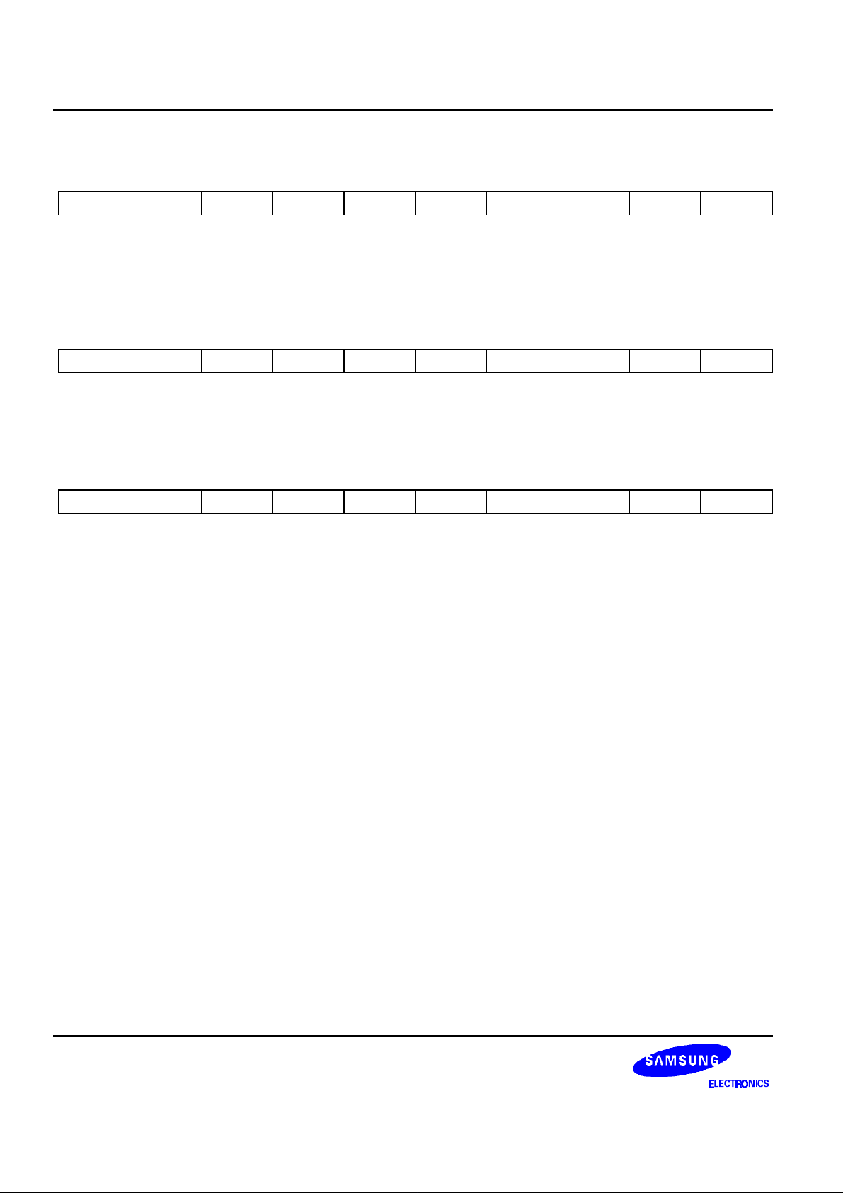
Display Clear
RS R/W DB7 DB6 DB5 DB4 DB3 DB2 DB1 DB0
0 0 0 0 0 0 0 0 0 1
Clear all the display data by writing "20H" (space code) to all DDRAM address, and set DDRAM address to "00H"
into AC (address counter). Return cursor to the original status, hence, bring the cursor to the left edge on first line
of the display. Entry mode is set to increment mode (I/D = "1")
Return Home
RS R/W DB7 DB6 DB5 DB4 DB3 DB2 DB1 DB0
0 0 0 0 0 0 0 0 1 X
Return Home is cursor return home instruction. Set DDRAM address to "00H" into the address counter. Return
cursor to its original site and return display to its original status, if shifted. Contents of DDRAM does not change.
Entry Mode Set
RS R/W DB7 DB6 DB5 DB4 DB3 DB2 DB1 DB0
0 0 0 0 0 0 0 1 I/D S
Set the moving direction of cursor and display.
I/D: Increment/decrement of DDRAM address (cursor or blink)
When I/D = "High", cursor/blink moves to right and DDRAM address is increased by 1.
When I/D = "Low", cursor/blink moves to left and DDRAM address is decreased by 1.
- CGRAM operates the same as DDRAM, when read from or write to CGRAM.
When S = "High", after DDRAM write, the entire display of all lines is shifted to the right (I/D = "0")or to the left
(I/D = "1") but it will seem as if the cursor does not move. When S = "Low", or DDRAM read, or CGRAM
read/write operation, shift of entire display is not performed.
18
Page 19

34COM/120SEG DRIVER & CONTROLLER FOR DOT MATRIX LCD S6A0079
Display ON / OFF Control
RS R/W DB7 DB6 DB5 DB4 DB3 DB2 DB1 DB0
0 0 0 0 0 0 1 D C B
Control display/cursor/blink ON/OFF 1bit register.
D: Display ON/OFF control bit
When D = "High", entire display is turned on.
When D = "Low", display is turned off, but display data is remained in DDRAM.
C: Cursor ON/OFF control bit
When C = "High", cursor is turned on.
When C = "Low", cursor is disappeared in current display, but I/D register remains its data.
B: Cursor Blink ON/OFF control bit
When B = "High", cursor blink is on, that performs alternate between all the high data and display
character at the cursor position. If fosc has 270kHz frequency, blinking has 370 ms interval.
When B = "Low", blink is off.
Cursor or Display Shift
RS R/W DB7 DB6 DB5 DB4 DB3 DB2 DB1 DB0
0 0 0 0 0 1 S/C R/L - -
Without writing or reading of display data, shift right/left cursor position or display. This instruction is used to
correct or search display data (refer to Table 7). During 2-line mode display, cursor moves to the 2nd line after
48th digit of 1st line. In 4-line mode, cursor moves to the next line, only after every 24th digit of the current line.
Note that display shift is performed simultaneously in all the line. When displayed data is shifted repeatedly, each
line shifted individually. When display shift is performed, the contents of address counter are not changed.
Table 7. Shift Patterns According to S/C and R/L Bits
S/C R/L Operation
0 0 Shift cursor to the left, address counter is decreased by 1
0 1 Shift cursor to the right, address counter is increased by 1
1 0 Shift all the display to the left, cursor moves according to the display
1 1 Shift all the display to the right, cursor moves according to the display
19
Page 20
S6A0079 34COM/120SEG DRIVER & CONTROLLER FOR DOT MATRIX LCD
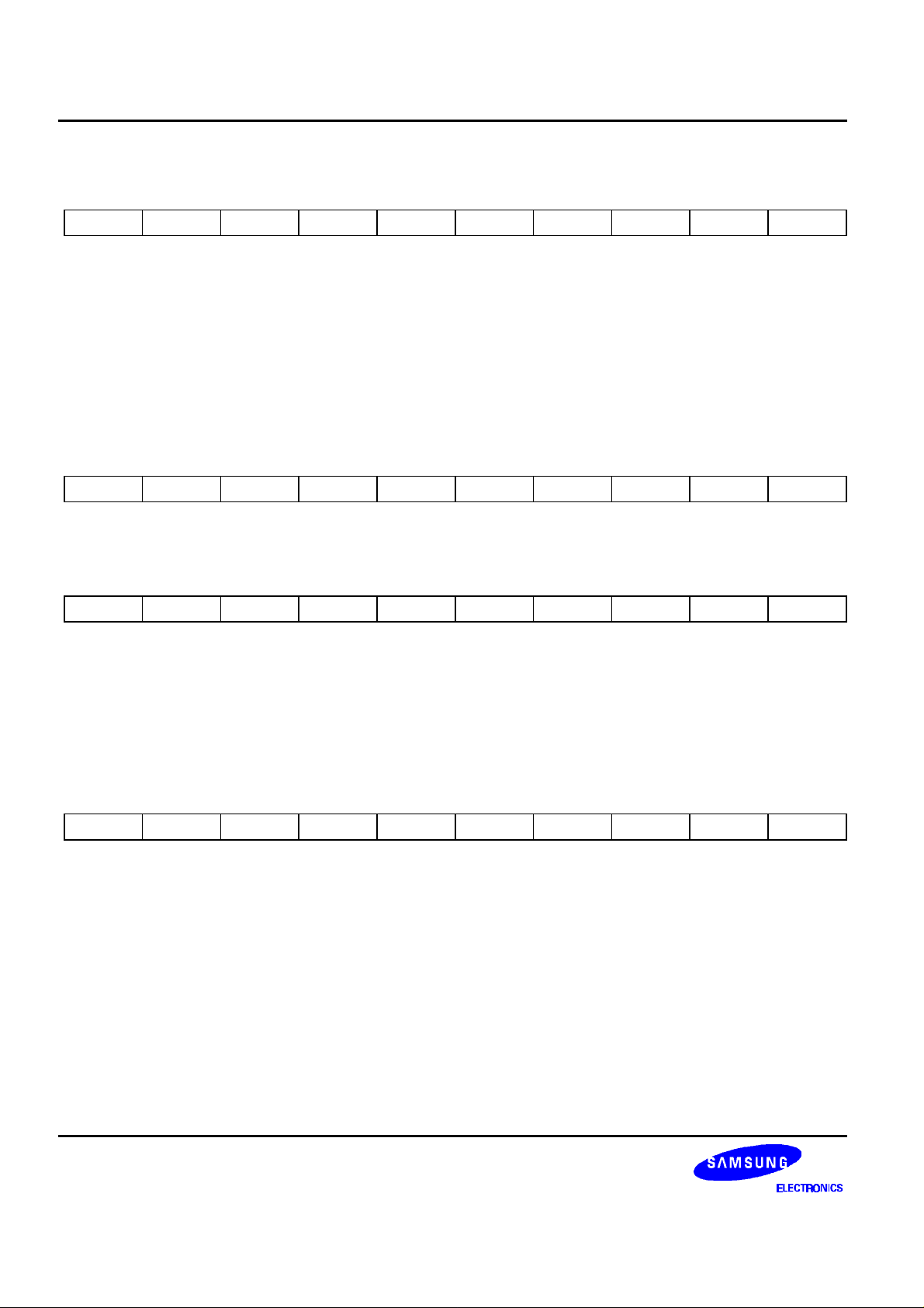
Function Set
RS R/W DB7 DB6 DB5 DB4 DB3 DB2 DB1 DB0
0 0 0 0 1 DL N X X X
DL: Interface data length control bit
When DL = "High", it means 8-bit bus mode with MPU.
When DL = "Low", it means 4-bit bus mode with MPU. Hence, DL is a signal to select 8-bit or 4-bit bus
mode.
In 4-bit bus mode, it is required to transfer 4-bit data by two times.
N: Display line number control bit
When N = "Low", it means 2-line display mode.
When N = "High", 4-line display mode is set.
Set CGRAM Address
RS R/W DB7 DB6 DB5 DB4 DB3 DB2 DB1 DB0
0 0 0 1 AC5 AC4 AC3 AC2 AC1 AC0
Set CGRAM address to AC. This instruction makes CGRAM data available from MPU.
Set DDRAM Address
RS R/W DB7 DB6 DB5 DB4 DB3 DB2 DB1 DB0
0 0 1 AC6 AC5 AC4 AC3 AC2 AC1 AC0
Set DDRAM address to AC. This instruction makes DDRAM data available from MPU.
In 2-line display mode (N = 0) DDRAM address in the 1st line is from "00H" to "2FH", and DDRAM address in the
2nd line is from "40H to 6FH".
In 4-line display mode (N = 1), DDRAM address is from "00H to "17H" in the 1st line, from "20H" to "37H" in the
2nd line, from "40H" to "57H" in the 3rd line and from "60H" to "77H" in the 4th line.
Read Busy Flag & Address
RS R/W DB7 DB6 DB5 DB4 DB3 DB2 DB1 DB0
0 1 BF AC6 AC5 AC4 AC3 AC2 AC1 AC0
This instruction shows whether S6A0079 is in internal operation or not. If the resultant BF is high, the internal
operation is in progress and you have to wait until BF to be low, which by then the next instruction can be
performed. In this instruction you can read the value of address counter.
20
Page 21
34COM/120SEG DRIVER & CONTROLLER FOR DOT MATRIX LCD S6A0079
Write Data to RAM
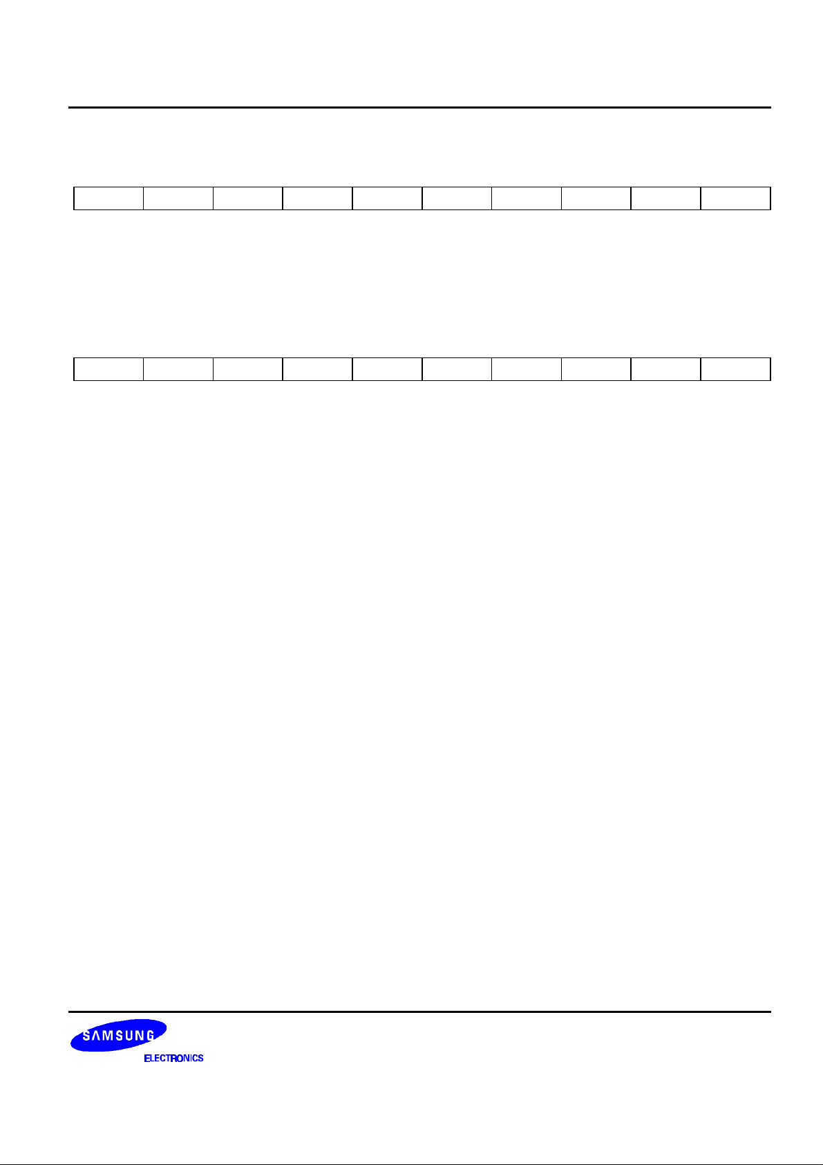
RS R/W DB7 DB6 DB5 DB4 DB3 DB2 DB1 DB0
1 0 D7 D6 D5 D4 D3 D2 D1 D0
Write binary 8-bit data to DDRAM/CGRAM. The selection of RAM from DDRAM, CGRAM is set by the previous
address set instruction : DDRAM address set, CGRAM address set. RAM set instruction can also determines the
AC direction to RAM. After write operation, the address is automatically increased/decreased by 1, according to
the entry mode.
Read Data From RAM
RS R/W DB7 DB6 DB5 DB4 DB3 DB2 DB1 DB0
1 1 D7 D6 D5 D4 D3 D2 D1 D0
Read binary 8-bit data from DDRAM/CGRAM. The selection of RAM is set by the previous address set
instruction. If address set instruction of RAM is not performed before this instruction, the data that read first is
invalid, as the direction of AC is not determined. If you read RAM data several times without RAM address set
instruction before read operation, the correct RAM data can be from the second, but the first data would be
incorrect, as there is no time margin to transfer RAM data. In DDRAM read operation, cursor shift instruction
plays the same role as DDRAM address set instruction : it also transfer RAM data to output data register. After
read operation address counter is automatically increased/decreased by 1 according to the entry mode. After
CGRAM read operation, display shift may not be executed correctly.
* In case of RAM write operation, AC is increased/decreased by 1 as in read operation after this. In this time, AC
indicates the next address position, but you can read only the previous data can only be read by read
instruction.
21
Page 22

S6A0079 34COM/120SEG DRIVER & CONTROLLER FOR DOT MATRIX LCD
INTERFACE WITH MPU
S6A0079 can transfer data in bus mode (4-bit or 8-bit) with MPU. Hence, both types of 4 or 8-bit MPU can be
used. In case of 4-bit bus mode, data transfer is performed by twice to transfer 1 byte data.
• When interfacing data length are 4-bit, only 4 ports, from DB4 to DB7, are used as data bus.
At first higher 4-bit (in case of 8-bit bus mode, the contents of DB4 - DB7) are transferred, and then lower 4bit (in case of 8-bit bus mode, the contents of DB0 - DB3) are transferred. So transfer is performed by twice.
busy flag outputs "High" after the second transfer is ended.
• When interfacing data length are 8-bit, transfer is performed at a time through 8 ports, from DB0 to DB7.
22
Page 23
34COM/120SEG DRIVER & CONTROLLER FOR DOT MATRIX LCD S6A0079
INTERFACE WITH MPU IN BUS MODE
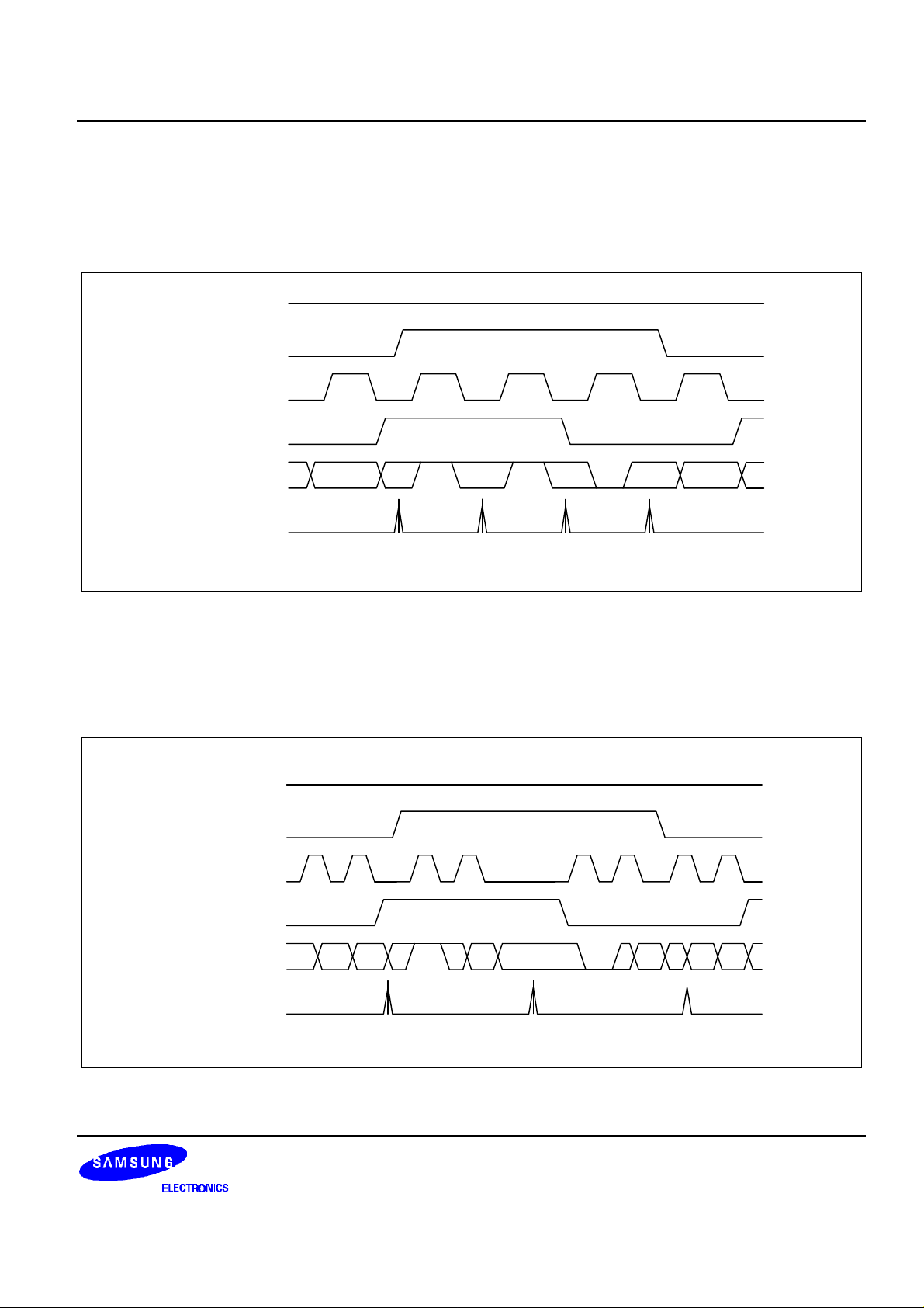
Interface with 8-bit MPU
If 8-bit MPU is used, S6A0079 can connect directly with that. In this case, port E, RS, R/W and DB0 to DB7 need
to interface each other. Example of timing sequence is shown below.
RS
R/W
E
Internal Signal
DB7
Data Busy Busy
Instruction
Internal Operation
Busy Flag
Check
Busy Flag
Check
No
Busy
Busy Flag
Check
Data
Instruction
Figure 5. Example of 8-bit Bus Mode Timing Sequence
Interface with 4-bit MPU
If 4-bit MPU is used, S6A0079 can connect directly with this. In this case, port E, RS, R/W and DB4 to DB7 need
to interface each other. The transfer is performed by twice. Example of timing sequence is shown below.
RS
R/W
E
Internal Signal
DB7
23
Internal Operation
D7 Busy
D3 D3AC3
Instruction Busy Flag Check Busy Flag Check Instruction
No
Busy
Figure 6. Example of 4-bit Bus Mode Timing Sequence
D7
Page 24
S6A0079 34COM/120SEG DRIVER & CONTROLLER FOR DOT MATRIX LCD
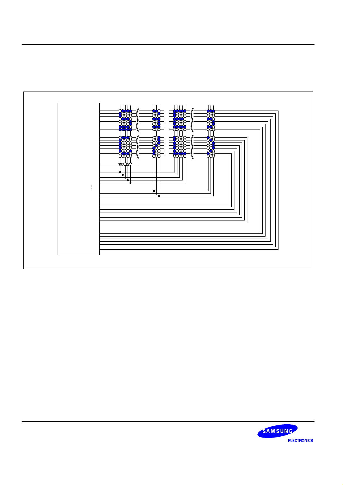
APPLICATION INFORMATION ACCORDING TO LCD PANEL
LCD Panel: 48 Character x 2-line Format
COM1
COM2
COM3
COM4
COM5
COM6
COM7
COM8
COM17
COM18
COM19
COM20
COM21
COM22
COM23
COM24
COM33
(COM0)
SEG1
SEG2
SEG3
SEG4
S6A0079
SEG5
SEG118
SEG119
SEG120
COM32
COM31
COM30
COM29
COM28
COM27
COM26
COM25
COM16
COM15
COM14
COM13
COM12
COM11
COM10
COM9
24
Page 25
34COM/120SEG DRIVER & CONTROLLER FOR DOT MATRIX LCD S6A0079
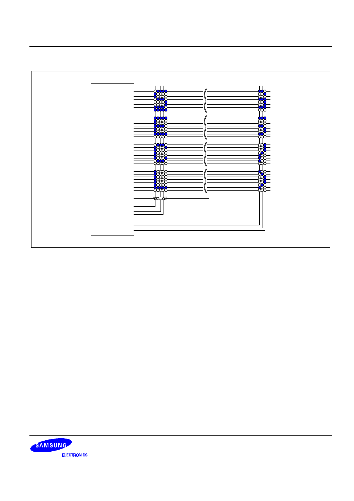
2) LCD Panel: 24 Character x 4-line Format
COM1
COM2
COM3
COM4
COM5
COM6
COM7
COM8
COM9
COM10
COM11
COM12
COM13
COM14
COM15
COM16
COM17
COM18
COM19
COM20
COM21
COM22
COM23
S6A0079
COM24
COM25
COM26
COM27
COM28
COM29
COM30
COM31
COM32
COM33
(COM0)
SEG1
SEG2
SEG3
SEG4
SEG5
SEG118
SEG119
SEG120
25
Page 26

S6A0079 34COM/120SEG DRIVER & CONTROLLER FOR DOT MATRIX LCD
INITIALIZING
INITIALIZING BY INTERNAL RESET CIRCUIT
When the power is turned on, S6A0079 is initialized automatically by power on reset circuit. During the
initialization, the following instructions are executed, and BF (Busy Flag) is kept "High" (busy state) to the end of
initialization.
Display Clear Instruction
Write "20H" to all DDRAM
Set Functions Instruction
DL = 1: 8-bit bus mode
N = 0: 2-line display mode
Control Display ON / OFF Instruction
D = 0: Display OFF
C = 0: Cursor OFF
B = 0: Blink OFF
Set Entry Mode Instruction
I/D = 1: Increment by 1
S = 0: No entire display shift
INITIALIZING BY HARDWARE RESET INPUT
When RESET pin = "Low", S6A0079 can be initialized like the case of power on reset. During the power on reset
operation, this pin is ignored.
26
Page 27
34COM/120SEG DRIVER & CONTROLLER FOR DOT MATRIX LCD S6A0079
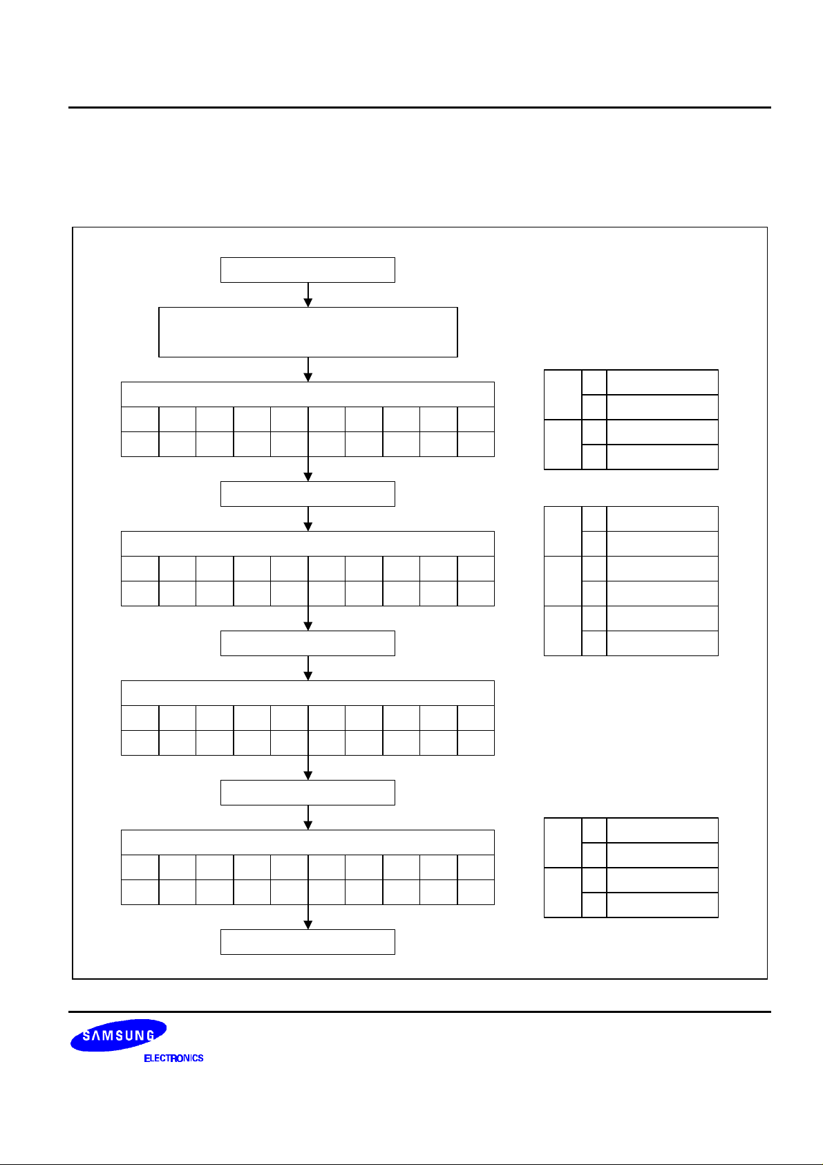
INITIALIZING BY INSTRUCTION
8-BIT INTERFACE MODE
Power On
Wait for more than 20ms after VDD rises to 4.5 V.
Wait for more than 30ms after VDD rises to 2.7 V.
(DL = "1")
Function Set
RS R/W DB7 DB6 DB5 DB4 DB3 DB2 DB1 DB0
0 0 0 0 1 DL(1) N x x x
Wait for more than 39µs
Display ON/OFF Control
RS R/W DB7 DB6 DB5 DB4 DB3 DB2 DB1 DB0
0 0 0 0 0 0 1 D C B
Wait for more than 39µs
Clear Display
RS R/W DB7 DB6 DB5 DB4 DB3 DB2 DB1 DB0
Condition: fosc = 270kHz
014-bit interface
DL
N
D
C
B
0
1
0
1
0
1
0
1
8-bit interface
1-line mode
2-bit interface
Display off
Display on
Cursor off
Cursor on
Blink off
Blink on
0 0 0 0 0 0 0 0 0 1
Wait for more than 1.53sms
Entry Mode Set
RS R/W DB7 DB6 DB5 DB4 DB3 DB2 DB1 DB0
0 0 0 0 0 0 0 1 I/D S
Initialization End
27
01Decrement mode
I/D
Increment mode
01Entire shift off
S
Entire shift on
Page 28
S6A0079 34COM/120SEG DRIVER & CONTROLLER FOR DOT MATRIX LCD
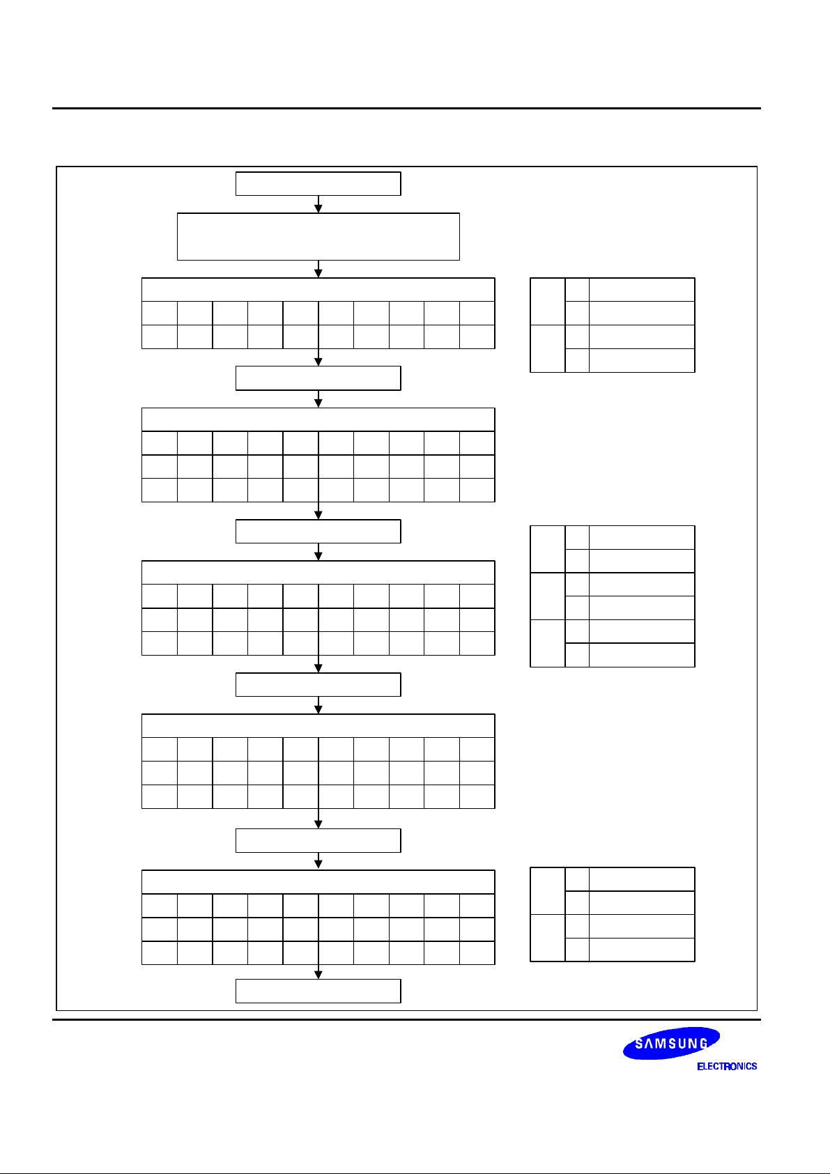
4-BIT INTERFACE MODE
Power On
Wait for more than 20ms after V DD rises to 4.5 V.
Wait for more than 30ms after V DD rises to 2.7 V.
(DL = "0")
Function Set
RS R/W DB7 DB6 DB5 DB4 DB3 DB2 DB1 DB0
Condition: fosc = 270kHz
014-bit interface
DL
8-bit interface
0 0 0 0 1 DL(0) x x x x
Wait for more than 39µs
Function Set
RS R/W DB7 DB6 DB5 DB4 DB3 DB2 DB1 DB0
0 0 0 0 1 0 x x x x
0 0 N x x x x x x x
Wait for more than 39µs
Display ON/OFF Control
RS R/W DB7 DB6 DB5 DB4 DB3 DB2 DB1 DB0
0 0 0 0 0 0 x x x x
0 0 1 D C B x x x x
Wait for more than 39µs
Display Clear
0
1
0
1
0
1
0
1
1-line mode
2-line mode
Display off
Display on
Cursor off
Cursor on
Blink off
Blink on
N
D
C
B
RS R/W DB7 DB6 DB5 DB4 DB3 DB2 DB1 DB0
0 0 0 0 0 0 x x x x
0 0 0 0 0 1 x x x x
Wait for more than 1.53 ms
Entry Mode Set
RS R/W DB7 DB6 DB5 DB4 DB3 DB2 DB1 DB0
0 0 0 0 0 0 x x x x
0 0 0 1 I/D S x x x x
Initialization End
01Decrement mode
I/D
Increment mode
01Entire shift off
S
Entire shift on
28
Page 29
34COM/120SEG DRIVER & CONTROLLER FOR DOT MATRIX LCD S6A0079
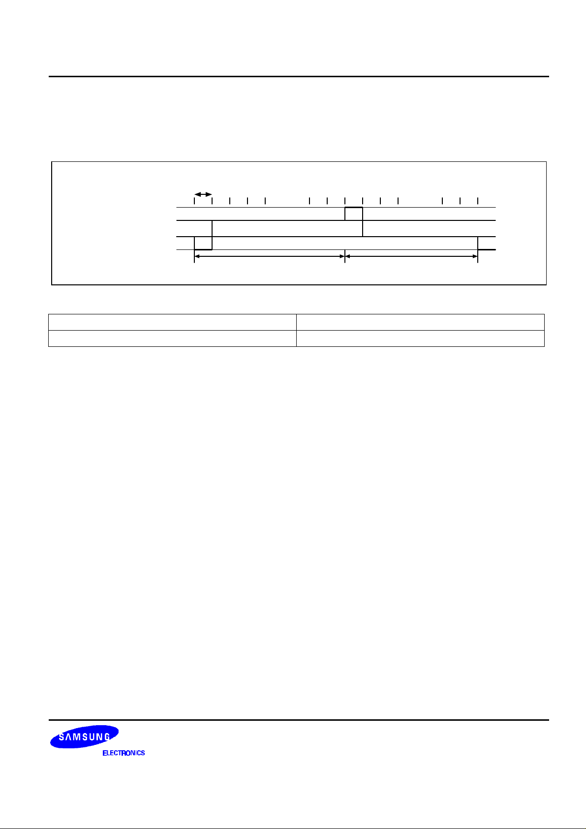
FRAME FREQUENCY
1/33 DUTY CYCLE
1-line selection period
VDD
V1
COM1
..
V4
V5
1-line selection period 120 clocks
Frame frequency 68.2Hz
fosc = 270kHz (1 clock = 3.7µs)
... ... 333232133324321
1 Frame 1 Frame
29
Page 30

S6A0079 34COM/120SEG DRIVER & CONTROLLER FOR DOT MATRIX LCD
POWER SUPPLY FOR DRIVING LCD PANEL
WHEN AN EXTERNAL POWER SUPPLY IS USED
VDD
WHEN AN INTERNAL BOOSTER IS USED
Boosting Twice
VDD
+
-
1µF
1µF
-
+
-
+
Vci
GND
C1
C2
V5OUT2
V5OUT3
Can be detached if
not using power
down mode
VDD
V1
V2
V3
V4
V5
R0
R
R
R
R
VEE
R
R
R0
R
R
VDD
V1
V2
V3
V4
V5
VDD
+
-
1µF
1µF
+
1µF
Boosting Three Times
Vci
GND
C1
-
+
-
-
+
C2
V5OUT2
V5OUT3
Can be detached if
not using power
down mode
VDD
V1
V2
V3
V4
V5
R
R
R0
R
R
30
Page 31
34COM/120SEG DRIVER & CONTROLLER FOR DOT MATRIX LCD S6A0079
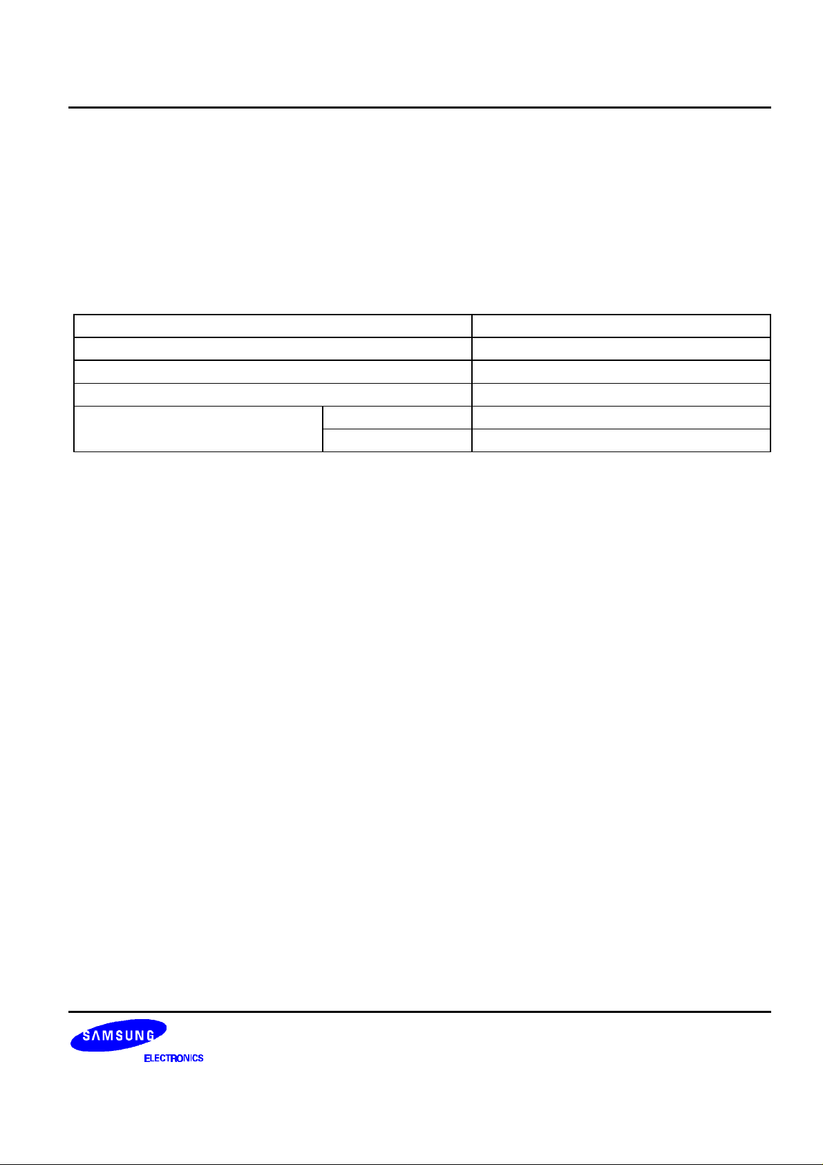
• Boosted output voltage should not exceed the maximum value (13 V) of the LCD driving voltage.
Especially, a voltage of over 4.3V should not be input to the reference voltage (Vci) when boosting three
times.
• A voltage of over 5.5V should not be input to the reference voltage (Vci) when boosting twice.
• The value of resistance, according to the number of lines, duty ratio and the bias, is shown below.
(refer to Table 8)
Table 8. Duty Ratio and Power Supply for LCD Driving
Item Data
Number of lines 2 or 4
Duty ration 1/33
Bias 1/6.7
Divided resistance R R
R0 2.7R
31
Page 32

S6A0079 34COM/120SEG DRIVER & CONTROLLER FOR DOT MATRIX LCD
MAXIMUM ABSOLUTE RATE
Characteristic Symbol Value Unit
Power supply voltage (1)
Power supply voltage (2)
Input voltage
Operating temperature
Storage temperature
Voltage greater than above may damage to the circuit (VDD ≥ V1 ≥ V2 ≥ V3 ≥ V4 ≥ V5)
VDD
V
VDD -15.0 to VDD +0.3
LCD
-0.3 to +7.0 V
VIN -0.3 to VDD +0.3
T
T
OPR
STG
-30 to +85
-55 to +125
V
V
°C
°C
32
Page 33
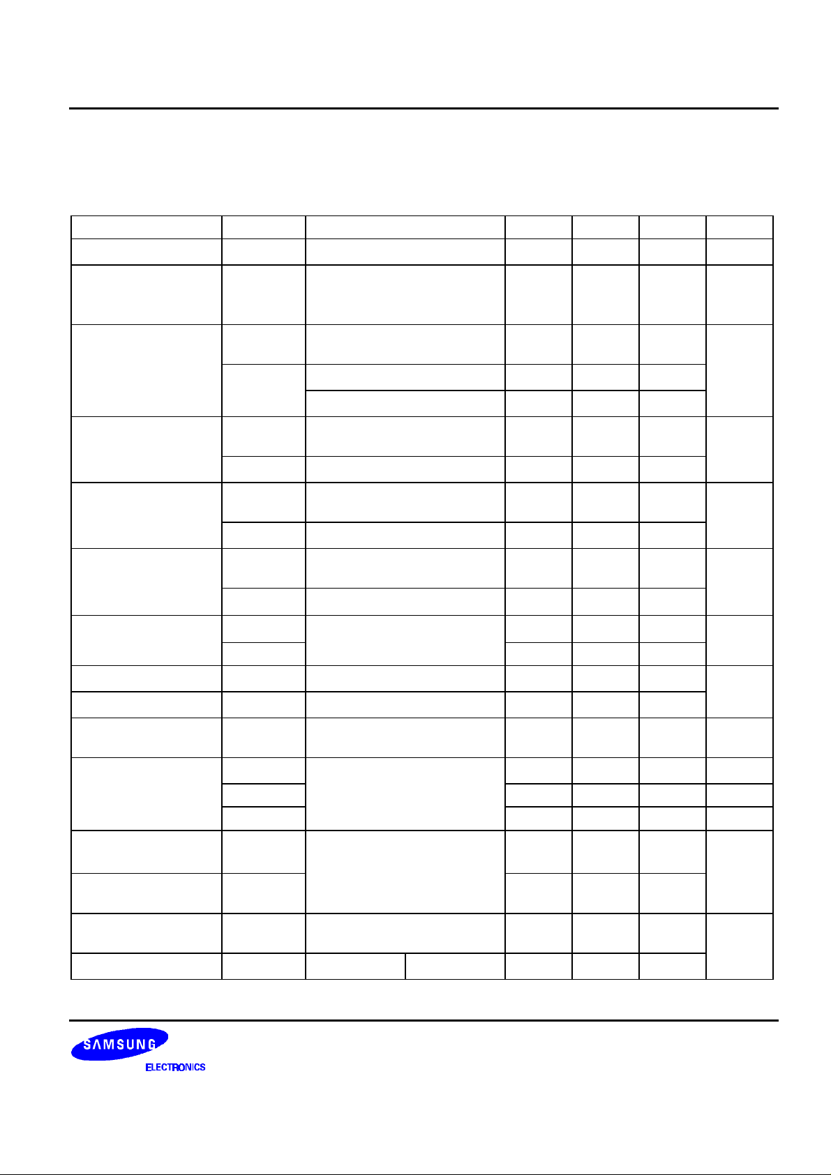
34COM/120SEG DRIVER & CONTROLLER FOR DOT MATRIX LCD S6A0079
ELECTRICAL CHARACTERISTICS
DC CHARACTERISTICS (VDD = 2.7V - 5.5V, Ta = -30 - +85°C)
Characteristic Symbol Condition Min Typ Max Unit
Operating voltage
VDD
- 2.7 - 5.5 V
Supply current
Input voltage (1)
(Except OSC1)
Input voltage (2)
(OSC1)
Output voltage (1)
(DB0 - DB7)
Output voltage(2)
(except DB0 - DB7)
Voltage drop Vd
Vd
Input leakage current
Low input current
Internal clock
(external Rf)
External clock
IDD
Internal oscillation or external
- 0.15 0.3 mA
clock.
(V
= 3.0V, fosc = 270kHz)
DD
V
IH1
V
V
IL1
V
IH2
V
IL2
V
I
OH1
V
I
OL1
V
OH2
V
OL1
COM
- - 1
SEG
IIL V
IIN V
fosc
= 2.7 - 3.0
DD
V
= 3.0 - 5.5
DD
= -0.1mA 0.75V
OH
= 0.1mA
OL
IO = -40µA
IO = 40µA
IO = ±0.1mA
= 0V - VDD
IN
= 0V, V
IN
Rf = 91kΩ ±2% (V
fEC
-
-
- - -
= 3V (pull up)
DD
= 5V)
DD
- 125 270 410 kHz
0.7V
DD
-0.3 -
-
VDD
0.2V
-0.3 - 0.6
0.7V
DD
-
VDD
0.2V
DD
- -
0.8V
DD
- -
- - V
0.2V
- - V
0.2V
- - 1 V
-1 - 1
-10 -50 -120
190 270 350 kHz
DD
DD
DD
DD
-
V
µA
duty 45 50 55 %
tr, tf - - 0.2
V
V
OUT2
OUT3
Ta = 25°C, C = 1µF,
I
= 0.25mA,
OUT
fosc = 270kHz -4.3 -5.1 -
-3.0 -4.2 - V
Voltage converter
OUT2 (Vci = 4.5V)
Voltage converter
OUT3 (Vci = 2.7V)
Voltage converter
Vci - 1.0 - 4.5 V
input
V
LCD driving voltage
VDD-V5
LCD
1/6.7 bias 3.0 - 13.0
33
µs
Page 34

S6A0079 34COM/120SEG DRIVER & CONTROLLER FOR DOT MATRIX LCD
AC CHARACTERISTICS (VDD = 4.5 - 5.5V, Ta = -30 - +85°C)
Mode Item Symbol
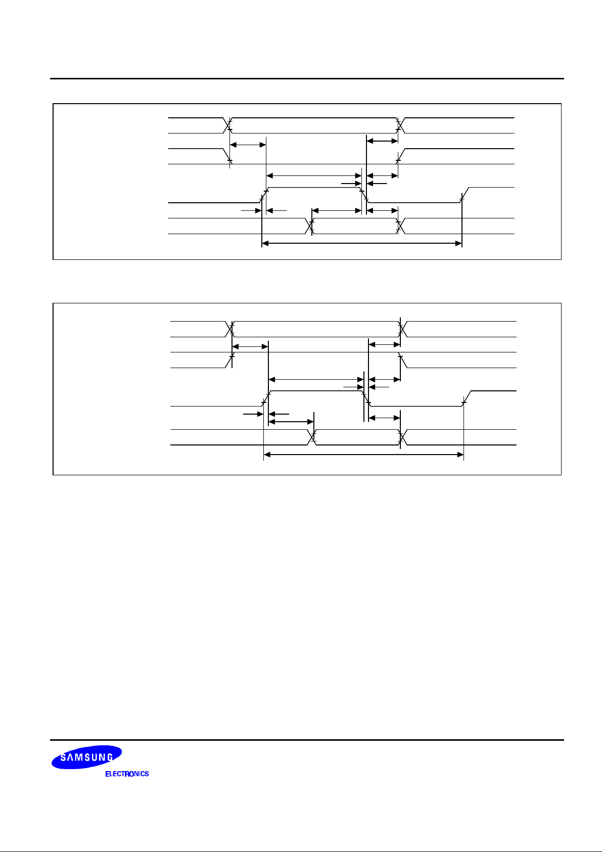
(1) Write mode E cycle time tc, 500 - - ns
Min Typ Max Unit
(refer to Figure 7) E rise/fall time tr, tf - - 20
E pulse width (high, low) tw 230 - -
R/W and RS setup time tsu1 40 - -
R/W and RS hold time th1 10 - -
Data setup time tsu2 60 - -
Data hold time th2 10 - -
(2) Read mode E cycle time tc 500 - - ns
(refer to Figure 8) E rise/fall time tr, tf - - 20
E pulse width (high, low) tw 230 - -
R/W and RS setup time tsu 40 - -
R/W and RS hold time th 10 - -
Data output delay time
Data hold time
tD
tDH
- - 160
5 - -
(VDD = 2.7 - 4.5V, Ta = -30 - +85°C)
Mode Item Symbol
(3) Write mode E cycle time tc, 1000 - - ns
Min Typ Max Unit
(refer to Figure 7) E rise / fall time tr, tf - - 25
E pulse width (high, low) tw 450 - -
R/W and RS setup time tsu1 60 - -
R/W and RS hold time th1 20 - -
Data setup time tsu2 195 - -
Data hold time th2 10 - -
(4) Read mode E cycle time tc 1000 - - ns
(refer to Figure 8) E rise / fall time tr, tf - - 25
E pulse width (high, low) tw 450 - -
R/W and RS setup time tsu 60 - -
R/W and RS hold time th 20 - -
Data output delay time
Data hold time
tD
tDH
- - 360
5 - -
34
Page 35
34COM/120SEG DRIVER & CONTROLLER FOR DOT MATRIX LCD S6A0079
V
RS
R/W
E
DB0 - DB7
IH1
V
IL1
t
su1
V
IL1
t
w
V
IH1
V
IL1
t
r
V
IH1
V
IL1
V
V
t
su2
Valid Data
IH1
t
h1
V
IL1
t
h1
t
f
V
IL1
t
h2
V
IH1
V
t
c
IL1
IL1
Figure 7. Write Mode
V
RS
R/W
E
DB0 - DB7
IH1
V
IL1
t
su
V
IH1
w
t
V
IH1
V
IL1
t
r
t
D
V
OH1
V
OL1
V
IH1
V
IL1
Valid Data
t
h
V
IH1
t
h
t
f
V
t
DH
V
OH1
V
t
c
OL1
IL1
Figure 8. Read Mode
35
Page 36
S6A0079 34COM/120SEG DRIVER & CONTROLLER FOR DOT MATRIX LCD
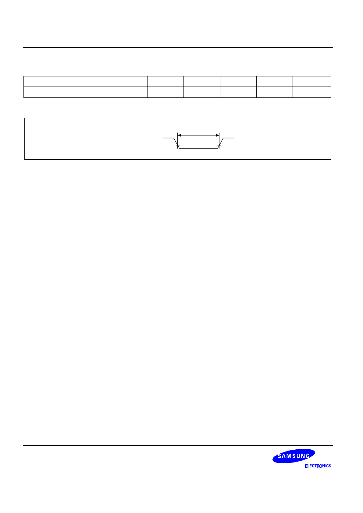
RESET TIMING (VDD = 2.7 - 5.5V, Ta = -30 - +85°C)
Item Symbol Min Typ Max Unit
t
Reset low level width (refer to Figure 9)
RES
10 - - ms
RES
t
RESET
IL1
V
IL1
V
Figure 9. Reset Timing Diagram
36
 Loading...