

Page 1

`
written permission of LCD Driver IC Team.
S6B0794
160 SEG / COM DRIVER FOR STN LCD
Contents in this document are subject to change without notice. No part of this document may be reproduced
or transmitted in any form or by any means, electronic or mechanical, for any purpose, without the express
July, 2000
Ver. 3.0
Prepared by: Gyeong-Nam, Kim
Page 2
160 SEG / COM DRIVER FOR STN LCD SPEC. VER. 3.0 S6B0794
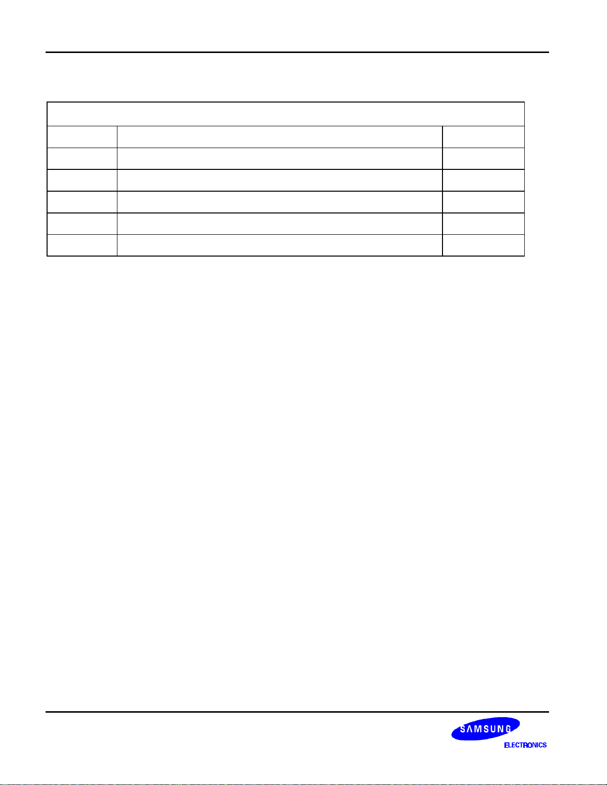
S6B0794 Specification Revision History
Version Content Date
0.0 l Original 1999. 4.15
1.0 l Including application note. 1999. 7.05
1.1 l p6, p16 revision. 1999. 8.17
2.0 l p4 Introduction revision. 2000.01.31
3.0 l p6,p8 dummy pad addition. 2000.07.21
2
Page 3

S6B0794 SPEC. VER 3.0 160 SEG / COM DRIVER FOR STN LCD
CONTENTS
INTRODUCTION ..................................................................................................................................................4
FEATURES..........................................................................................................................................................4
BLOCK DIAGRAM...............................................................................................................................................5
PAD CONFIGURATION .......................................................................................................................................6
PAD CENTER COORDINATES ............................................................................................................................7
PIN DESCRIPTION ..............................................................................................................................................9
FUNCTIONAL DESCRIPTION............................................................................................................................ 10
BLOCK FUNCTION.....................................................................................................................................10
PIN FUNCTION...........................................................................................................................................11
FUNCTIONAL OPERATIONS......................................................................................................................15
SPECIFICATIONS..............................................................................................................................................18
ABSOLUTE MAXIMUM RATINGS...............................................................................................................18
RECOMMENDED OPERATING CONDITIONS ...........................................................................................18
DC CHARACTERISTICS.............................................................................................................................19
AC CHARACTERISTICS.............................................................................................................................21
PRECAUTION.................................................................................................................................................... 27
CONNECTION EXAMPLES OF PLURAL SEGMENT DRIVERS........................................................................28
TIMING CHART OF 4-DEVICE CASECADE CONNECTION OF SEGMENT DRIVERS......................................29
CONNECTION EXAMPLES OF PLURAL COMMON DRIVERS.........................................................................30
3
Page 4

160 SEG / COM DRIVER FOR STN LCD SPEC. VER. 3.0 S6B0794
INTRODUCTION
The S6B0794 is a 160-outputs segment/common driver LSI for graphic dot-matrix liquid
crystal display systems. It is fabricated by low power CMOS high voltage process technology.
This device consists of 160-bits bi-directional shift register, 160-bits data latch and 160-bits
driver. In case of segment mode, the data input is selected 4bit parallel input mode and 8bit
parallel input mode by a mode (MD) pin. In case of common mode, data input/output pins are
bi-directional, four data shift directions are pin-selectable.
FEATURES
Both Segment Mode and Common Mode
- Supply voltage for LC driver: +15.0 to +32.0V
- Number of LC driver outputs: 160
- Low output impedance
- Low power consumption
- Supply voltage for the logic system: +2.4V to +5.5V
- CMOS silicon gate process (P-type Silicon Substrate)
- Package: 190-pin TCP (Tape Carrier Package) & Gold bumped chip
Segment Mode
- Shift clock frequency: 14MHz (Max) (Vdd=+5V±10%)
8MHz (Max) (Vdd=+2.4V to +4.5V)
- Adopts a data bus system
- 4-bit / 8-bit parallel input modes are selectable with a mode (MD) pin
- Automatic transfer function of an enable signal
- Automatic counting function which, in the chip select, causes the internal clock to be stopped
by automatically counting 160 of input data
- Line latch circuit reset function when DISPOFFB active
Common Mode
- Shift clock frequency: 4.0MHz (Max) (vdd=+2.4V to +5.5V)
- Built-in 160 bits bi-directional shift register (divisible into 80-bits ×2)
- Available in a single mode (160-bits shift register) or in a dual mode(80-bits shift register ×2)
- Shift register circuit reset function when DISPOFFB active
4
Page 5

S6B0794 SPEC. VER 3.0 160 SEG / COM DRIVER FOR STN LCD
BLOCK DIAGRAM
FR
DISPOFFB
EIO1
EIO2
LP
XCK
L/R
MD
182
179
181
169
180
178
166
183
VOR V12R
190 189 188 164
V43R V5L
LEVEL
SHIFTER
ACTIVE
CONTROL
CONTROL
LOGIC
8
8BITS*2
DATA
LATCH
Y160Y159Y1 Y2
1 2 160159
160 BITS 4-LEVEL DRIVER
160
160 BITS LEVEL SHIFTER
160
160 BITS LINE LATCH/SHIFTER
REGISTER
16 16
16
16 16
16
16 16
16
DATA LATCH CONTROL
16
187
163
162
161
V5L
V43L
V12L
VOL
S/C
168
SP CONVERSION & DATA CONTROL
(4 to 8 or 8to 8)
170 171 172 173 174 175 176 177 165 186167
D I0 D I1 D
I
2 D I3 DI4 DI5 DI6 DI7
Figure 1. Block Diagram
VDD
VSS VSS
5
Page 6
160 SEG / COM DRIVER FOR STN LCD SPEC. VER. 3.0 S6B0794
1
160
ð ð ð ð ð ð ð ð ð ð ð ð ð ð ð ð ð ð
ð
ð
ð
ð
ð
ð
ð
ð
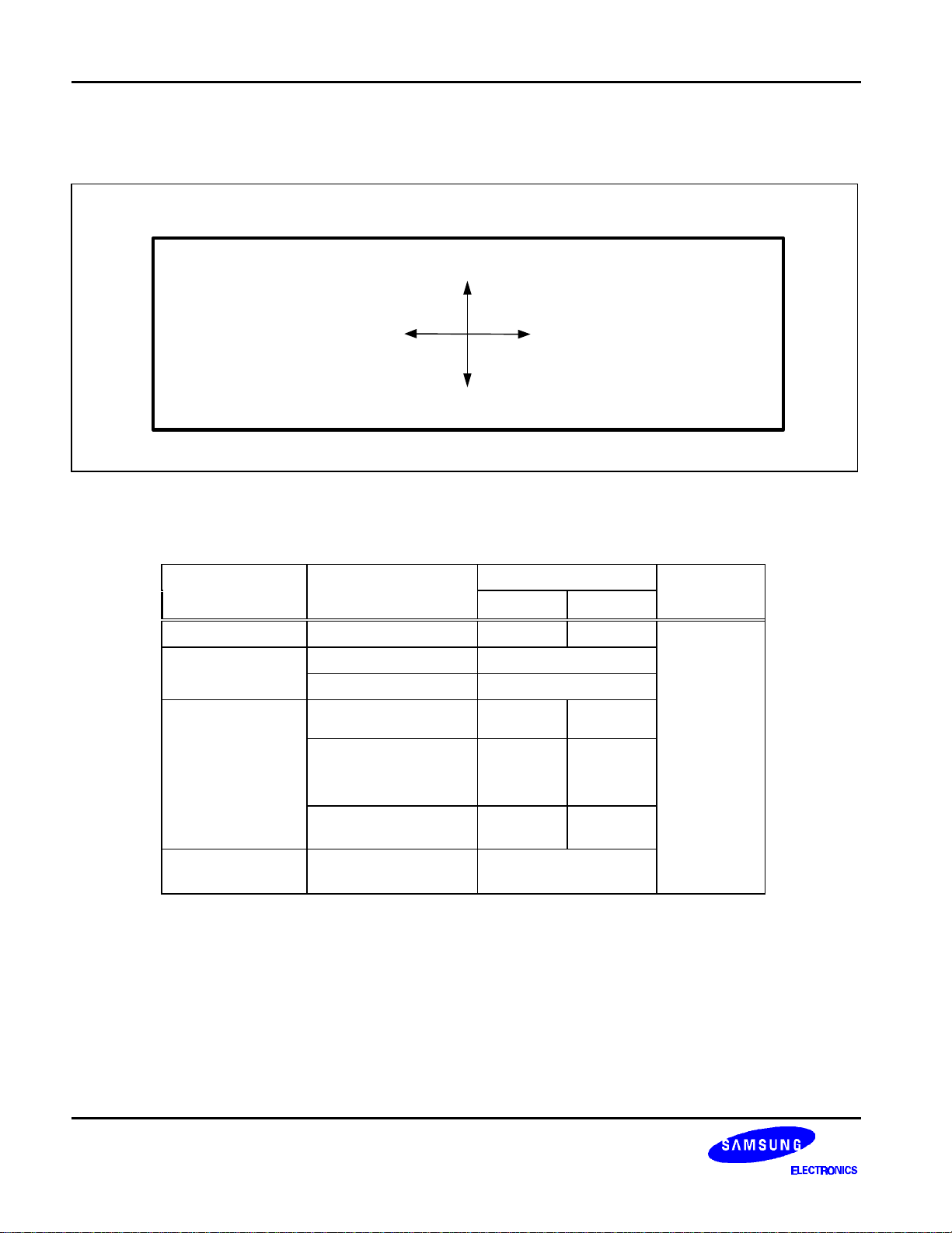
PAD CONFIGURATION
161
ррррррррррррррррррррр
- - - - - - - - - -
Y
рррррррррррррррррррр
S6B0794
(TOP VIEW, Pads Up)
(0,0)
X
ð ð ð ð ð ð ð ð ð ð ð ð ð ð
Figure 2. S6B0794 Chip Configuration
Table 1. S6B0794 Pad Dimensions
ITEM PAD NO.
CHIP SIZE - 11000 1100
1 to 160 65 (MIN)
PAD PITCH
161 to 190 260 (MIN)
1 to 160
SIZE
X Y
43 108
190
186 DummyDummy 165
187164
UNIT
161 to 164
BUMPED
PAD SIZE
BUMPED
PAD HEIGHT
6
187 to 190
165 to 186 58 76
1 to 190 14 (Typ)
76 58
µm
Page 7
S6B0794 SPEC. VER 3.0 160 SEG / COM DRIVER FOR STN LCD
50
Y50
1982.5
395
100
Y100
-1267.5
395
150
Y150
-4517.5
395
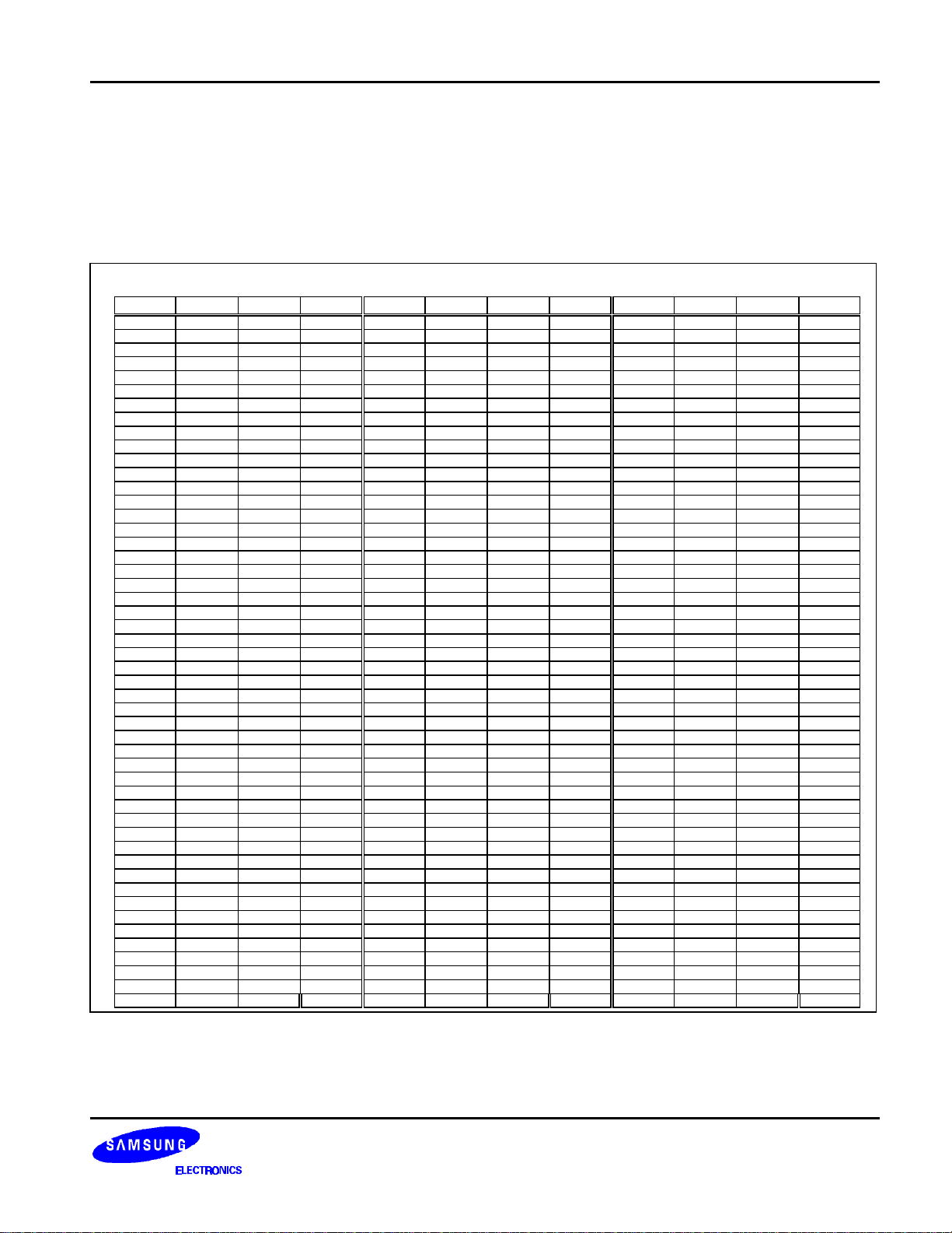
PAD CENTER COORDINATES
Table 2. Pad Location
[Unit: µm]
NO NAME X Y NO NAME X Y NO NAME X Y
1 Y1 5167.5 395 51 Y51 1917.5 395 101 Y101 -1332.5 395
2 Y2 5102.5 395 52 Y52 1852.5 395 102 Y102 -1397.5 395
3 Y3 5037.5 395 53 Y53 1787.5 395 103 Y103 -1462.5 395
4 Y4 4972.5 395 54 Y54 1722.5 395 104 Y104 -1527.5 395
5 Y5 4907.5 395 55 Y55 1657.5 395 105 Y105 -1592.5 395
6 Y6 4842.5 395 56 Y56 1592.5 395 106 Y106 -1657.5 395
7 Y7 4777.5 395 57 Y57 1527.5 395 107 Y107 -1722.5 395
8 Y8 4712.5 395 58 Y58 1462.5 395 108 Y108 -1787.5 395
9 Y9 4647.5 395 59 Y59 1397.5 395 109 Y109 -1852.5 395
10 Y10 4582.5 395 60 Y60 1332.5 395 110 Y110 -1917.5 395
11 Y11 4517.5 395 61 Y61 1267.5 395 111 Y111 -1982.5 395
12 Y12 4452.5 395 62 Y62 1202.5 395 112 Y112 -2047.5 395
13 Y13 4387.5 395 63 Y63 1137.5 395 113 Y113 -2112.5 395
14 Y14 4322.5 395 64 Y64 1072.5 395 114 Y114 -2177.5 395
15 Y15 4257.5 395 65 Y65 1007.5 395 115 Y115 -2242.5 395
16 Y16 4192.5 395 66 Y66 942.5 395 116 Y116 -2307.5 395
17 Y17 4127.5 395 67 Y67 877.5 395 117 Y117 -2372.5 395
18 Y18 4062.5 395 68 Y68 812.5 395 118 Y118 -2437.5 395
19 Y19 3997.5 395 69 Y69 747.5 395 119 Y119 -2502.5 395
20 Y20 3932.5 395 70 Y70 682.5 395 120 Y120 -2567.5 395
21 Y21 3867.5 395 71 Y71 617.5 395 121 Y121 -2632.5 395
22 Y22 3802.5 395 72 Y72 552.5 395 122 Y122 -2697.5 395
23 Y23 3737.5 395 73 Y73 487.5 395 123 Y123 -2762.5 395
24 Y24 3672.5 395 74 Y74 422.5 395 124 Y124 -2827.5 395
25 Y25 3607.5 395 75 Y75 357.5 395 125 Y125 -2892.5 395
26 Y26 3542.5 395 76 Y76 292.5 395 126 Y126 -2957.5 395
27 Y27 3477.5 395 77 Y77 227.5 395 127 Y127 -3022.5 395
28 Y28 3412.5 395 78 Y78 162.5 395 128 Y128 -3087.5 395
29 Y29 3347.5 395 79 Y79 97.5 395 129 Y129 -3152.5 395
30 Y30 3282.5 395 80 Y80 32.5 395 130 Y130 -3217.5 395
31 Y31 3217.5 395 81 Y81 -32.5 395 131 Y131 -3282.5 395
32 Y32 3152.5 395 82 Y82 -97.5 395 132 Y132 -3347.5 395
33 Y33 3087.5 395 83 Y83 -162.5 395 133 Y133 -3412.5 395
34 Y34 3022.5 395 84 Y84 -227.5 395 134 Y134 -3477.5 395
35 Y35 2957.5 395 85 Y85 -292.5 395 135 Y135 -3542.5 395
36 Y36 2892.5 395 86 Y86 -357.5 395 136 Y136 -3607.5 395
37 Y37 2827.5 395 87 Y87 -422.5 395 137 Y137 -3672.5 395
38 Y38 2762.5 395 88 Y88 -487.5 395 138 Y138 -3737.5 395
39 Y39 2697.5 395 89 Y89 -552.5 395 139 Y139 -3802.5 395
40 Y40 2632.5 395 90 Y90 -617.5 395 140 Y140 -3867.5 395
41 Y41 2567.5 395 91 Y91 -682.5 395 141 Y141 -3932.5 395
42 Y42 2502.5 395 92 Y92 -747.5 395 142 Y142 -3997.5 395
43 Y43 2437.5 395 93 Y93 -812.5 395 143 Y143 -4062.5 395
44 Y44 2372.5 395 94 Y94 -877.5 395 144 Y144 -4127.5 395
45 Y45 2307.5 395 95 Y95 -942.5 395 145 Y145 -4192.5 395
46 Y46 2242.5 395 96 Y96 -1007.5 395 146 Y146 -4257.5 395
47 Y47 2177.5 395 97 Y97 -1072.5 395 147 Y147 -4322.5 395
48 Y48 2112.5 395 98 Y98 -1137.5 395 148 Y148 -4387.5 395
49 Y49 2047.5 395 99 Y99 -1202.5 395 149 Y149 -4452.5 395
7
Page 8

160 SEG / COM DRIVER FOR STN LCD SPEC. VER. 3.0 S6B0794
Table 3. Pad Location(Continued)
[Unit: µm]
NO NAME X Y
151 Y151 -4582.5 395
152 Y152 -4647.5 395
153 Y153 -4712.5 395
154 Y154 -4777.5 395
155 Y155 -4842.5 395
156 Y156 -4907.5 395
157 Y157 -4972.5 395
158 Y158 -5037.5 395
159 Y159 -5102.5 395
160 Y160 -5167.5 395
161 VOL -5369 330
162 V12L -5369 90
163 V43L -5369 -120
164 V5L -5369 -330
DUMMY1 -4860 -419
165 VSS -4600 -419
166 LR -4340 -419
167 VDD -4080 -419
168 SC -3820 -419
169 EIO2 -3560 -419
170 DI0 -3300 -419
171 DI1 -3040 -419
172 DI2 -2780 -419
173 DI3 -2520 -419
174 DI4 -2260 -419
175 DI5 -2000 -419
176 DI6 -1740 -419
177 DI7 -1480 -419
DUMMY -1380 -419
DUMMY -1280 -419
DUMMY -1180 -419
DUMMY -1080 -419
DUMMY 1990 -419
DUMMY 2090 -419
DUMMY 2190 -419
178 XCK 2290 -419
179 DISPOFFB 2550 -419
180 LP 2810 -419
181 EIO1 3070 -419
182 FR 3330 -419
183 MD 3590 -419
184 NC 3850 -419
185 NC 4110 -419
186 VSS 4370 -419
DUMMY2 4630 -419
DUMMY 5070 -419
187 V5R 5369 -330
188 V43R 5369 -120
189 V12R 5369 90
190 V0R 5369 330
8
Page 9

S6B0794 SPEC. VER 3.0 160 SEG / COM DRIVER FOR STN LCD
PIN DESCRIPTION
Table 3. Pin Description
Pin No. Symbol I/O Description
1 to 160
161, 190
162, 189
163, 188
164, 187
166
167
168
169
170 to
176
177
178
179
180
181
182
Y1 – Y160 O LC driver output
V0L, V0R - Power supply for LC driver
V12L, V12R - Power supply for LC driver
V43L, V43R - Power supply for LC driver
V5L, V5R - Power supply for LC driver
L/R I Display data shift direction selection
VDD - Power supply for logic system(+2.4 to +5.5V)
S/C I Segment mode/common mode selection
EIO2 I/O Input/output for chip select or data of shift register
DI0 – DI6 I Display data input for segment mode
DI7 I Display data input for segment mode/Dual mode data input
XCK I Display data shift clock input for segment mode
DISPOFFB I Control input for deselect output level
LP I Latch pulse input/shift clock input for shift register
EIO1 I/O Input/output for chip select or data of shift register
FR I AC-converting signal input for LC driver waveform
183
165, 186
MD I Mode selection input
VSS - Ground(0V)
9
Page 10

160 SEG / COM DRIVER FOR STN LCD SPEC. VER. 3.0 S6B0794
FUNCTIONAL DESCRIPTION
BLOCK FUNCTION
. Active Control
In case of segment mode, controls the selection or deselection of the chip. Following a LP
signal, and after the chip select signal is input, a select signal is generated internally until 160
bits of data have been read in. Once data input has been completed, a select signal for
cascade connection is output, and the chip is deselected. In case of common mode, controls
the input/output data of bidirectional pins.
. SP Conversion and Data Control
In case of segment mode, keep input data which are 2 clocks of XCK at 4-bit parallel mode into
latch circuit, or keep input data which are 1 clock of XCK at 8-bits parallel mode into latch
circuit, after that they are put on the internal data bus 8 bits at a time.
. Data Latch Control
In case of segment mode, selects the state of the data latch which reads in the data bus
signals. The shift direction is controlled by the control logic, for every 16 bits of data read in, the
selection signal shifts one bit based on the state of the control circuit.
. Data Latch
In case of segment mode, latches the data on the data bus. The latched state of each LC
driver output pin is controlled by the control logic and the data latch control, 160 bits of data are
read in 20 sets of 8 bits.
. Line Latch / Shift Register
In case of segment mode, all 160 bits which have been read into the data latch are
simultaneously latched on the falling edge of the LP signal, and output to the level shifter block.
In case of common mode, shifts data from the data input pin on the falling edge of the LP
signal.
. Level Shifter
The logic voltage signal is level-shifted to the LC driver voltage level, and output to the driver
block.
. 4-level Driver
Driver the LC driver output pins from the line latch/shift register data, selecting one of 4
levels(V0, V12, V43, V5) based on the S/C, FR and DISPOFFB signals.
. Control Logic
Controls the operation of each block. In case of segment mode, when a LP signal has been
input, all blocks are reset and the control logic waits for the selection signal output from the
active control block. Once the selection signal has been output, operation of the data latch and
data transmission are controlled, 160 bits of data are read in, and the chip is deselected. In
case of common mode, controls the direction of data shift.
10
Page 11

S6B0794 SPEC. VER 3.0 160 SEG / COM DRIVER FOR STN LCD
PIN FUNCTION
Segment Mode
Symbol Function
VDD
VSS
V0R, V0L
V12R , V12L
V43R , V43L
DI0 – DI7
XCK
LP
L/R
Logic system power supply pin connects to +2.4 to +5.5V
Ground pin connects to 0 V
Power supply pin for LC driver voltage bias.
. Normally, the bias voltage used is set by a resistor divider.
. Ensure that voltage are set such that VSS<V43<V12<V0.
. To further reduce the difference between the output waveforms of LC driver
output pins Y1 and Y160, externally connect ViR and ViL(i=0, 12, 43)
Input pin for display data
. In 4-bit parallel input mode, input data into the 4 pins DI0 – DI3.
Connect DI4 – DI7 to VSS or VDD.
. In 8-bit parallel input mode, input data into the 8 pins DI0 – DI7.
Clock input pin for taking display data
. Data is read on the falling edge of the clock pulse.
Latch pulse input pin for display data
. Data is latched on the falling edge of the clock pulse.
Direction selection pin for reading display data
. When set to VSS level “L”, data is read sequentially from Y160 to Y1.
DISPOFFB
. When set to VDD level H”, data is read sequentially from Y1 to Y160.
Control input pin for output deselect level
. The input signal is level-shifted from logic voltage level to LC drive voltage
level, and controls LC drive circuit.
. When set to VSS level “L”, the LC drive output pins (Y1-Y160) are set to level
VSS.
. While set to “L”, the contents of the line latch are reset, but read the display
data in the data latch regardless of condition of DISPOFFB.
When the DISPOFFB function is canceled, the driver outputs deselect
level(V12 or V43), then outputs the contents of the data latch on the next
falling edge of the LP. That time, if DISPOFFB removal time can not keep
regulation what is shown AC characteristics (page 21), can not output the
reading data correctly.
11
Page 12

160 SEG / COM DRIVER FOR STN LCD SPEC. VER. 3.0 S6B0794
AC signal input for LC driving waveform
. The input signal is level-shifted from logic voltage level to LC drive voltage
level, and controls LC drive circuit.
FR
. Normally, inputs a frame inversion signal.
. The LC driver output pin’s output voltage level can be set using the line
latch output signal and the FR signal.
Table of truth values is shown in Table 4.
Mode selection pin
MD
S/C
EIO1
EIO2
Y1 – Y160
. When set to VSS level “L”, 4-bit parallel input mode is set.
. When set to VDD level “H”, 8-bit parallel input mode is set.
. The relationship between the display data and driver output pins is shown
in Table 5.
Segment mode/common mode selection pin
. When set to VDD level ‘H”, segment mode is set.
Input/output pin for chip selection
. When L/R input is at VSS level ‘L”, EIO1 is set for output, and EIO2 is set for
input.
. When L/R input is at VDD level ‘H”, EIO1 is set for input, and EIO2 is set for
output.
. During output. set to “H” while LP*XCLKB is ‘H” and after 160-bits of data
have been read, set to “L” for one cycle (from falling edge to falling edge of
XCK), after which it returns to “H”.
. During input, after the LP signal is input, the chip is selected while EI is set
to “L”. After 160-bits of data have been read, the chip is deselected.
LC driver output pins
. Corresponding directly to each bit of the data latch, one level(V0, V12, V43,
or VSS) is selected and output.
12
Table of truth values is shown in Table 4.
Page 13
S6B0794 SPEC. VER 3.0 160 SEG / COM DRIVER FOR STN LCD
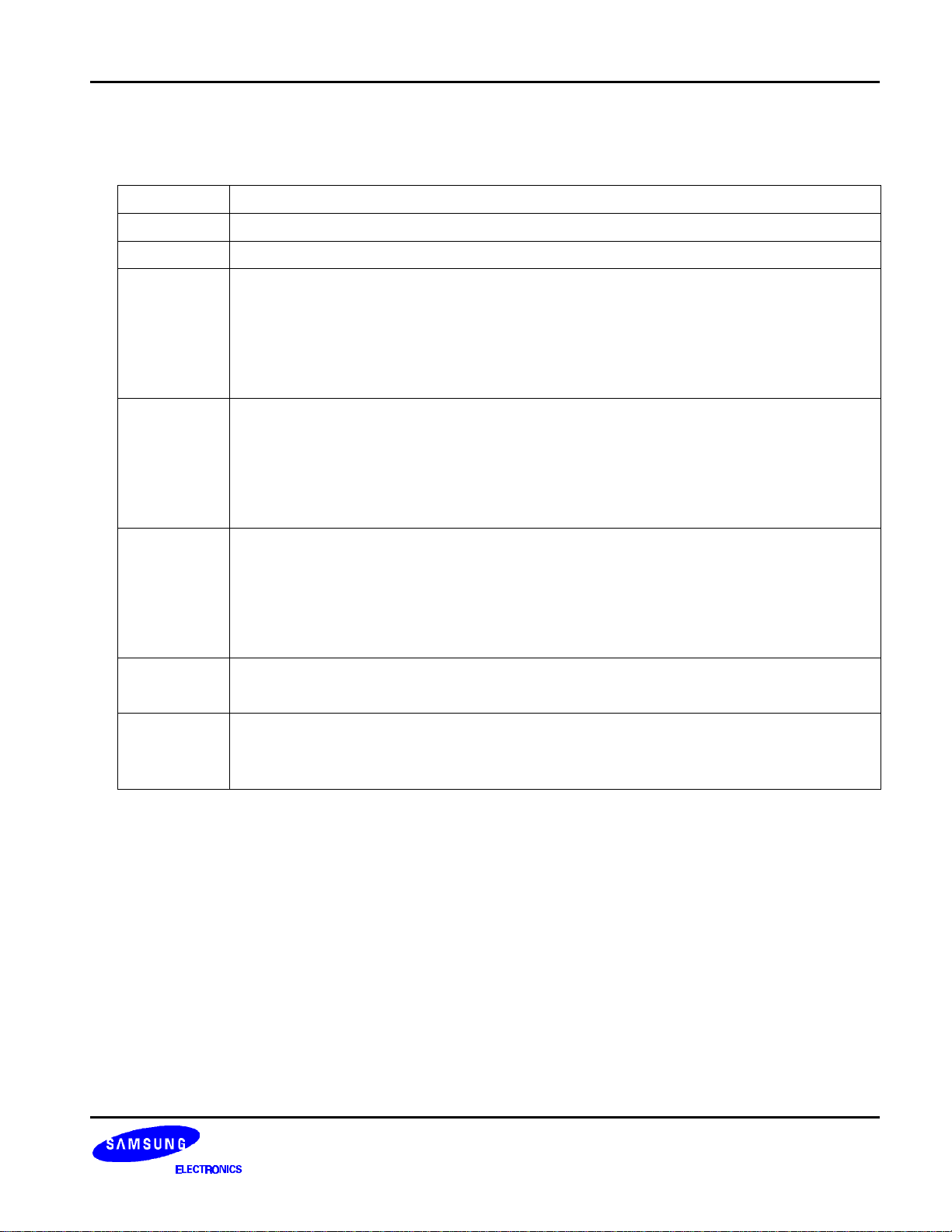
Common Mode
Symbol Function
VDD
VSS
V0R, V0L
V12R , V12L
V43R , V43L
EIO1
EIO2
LP
Logic system power supply pin connects to +2.4 to +5.5V
Ground pin connects to 0 V
Power supply pin for LC driver voltage bias.
. Normally, the bias voltage used is set by a resistor divider.
. Ensure that voltage are set such that VSS<V43<V12<V0.
. To further reduce the difference between the output waveforms of LC driver
output pins Y1 and Y160, externally connect ViR and ViL(i=0, 12, 43)
Bidirectional shift register shift data input/output pin
. Output pin when L/R is at VSS level “L”, input pin when L/R is at VDD level
“H”.
. When EIO1 is used as input pin, it will be pull-down.
. When EIO1 is used as output pin, it won’t be pull-down.
Bidirectional shift register shift data input/output pin
. Input pin when L/R is at VSS level “L”, output pin when L/R is at VDD level
“H”.
. When EIO2 is used as input pin, it will be pull-down.
. When EIO2 is used as output pin, it won’t be pull-down.
Bidirectional shift register shift clock pulse input pin
. Data is shifted on the falling edge of the clock pulse.
L/R
Bidirectional shift register shift direction selection pin
. Data is shifted from Y160 to Y1 when set to VSS to level “L”, and data is
shifted from Y1 to Y160 when set to VDD level “H”.
13
Page 14

160 SEG / COM DRIVER FOR STN LCD SPEC. VER. 3.0 S6B0794
Control input pin for output deselect level
. The input signal is level-shifted from logic voltage level to LC drive voltage
level, and controls LC drive circuit.
. When set to VSS level “L”, the LC drive output pins(Y1-Y160) are set to level
VSS.
DISPOFFB
. While set to “L”, the contents of the shift resister are reset not reading data.
When the DISPOFFB function is canceled, the driver outputs deselect
level(V12 or V43), and the shift data is reading on the falling edge of the LP.
That time, if DISPOFFB removal time can not keep regulation what is shown
AC characteristics (page 25), the shift data is not reading correctly.
AC signal input for LC driving waveform
. The input signal is level-shifted from logic voltage level to LC drive voltage
level, and controls LC drive circuit.
FR
MD
DI7
S/C
DI0 – DI6
XCK
. Normally, input a frame inversion signal.
. The LC driver output pin’s output voltage level can be set using the shift
register output signal and the FR signal.
Table of truth values is shown in Table4.
Mode selection pin
. When set to VSS level “L”, Single mode operation is selected, when set to
VDD level “H”, Dual mode operation is selected.
Dual Mode data input pin
. According to the data shift direction of the data shift register, data can be
input starting from the 81st bit.
When the chip is used as Dual mode, DI7 will be pull-down.
When the chip is used as Single mode, DI7 won’t be pull-down.
Segment mode/common mode selection pin
. When set to VSS level ‘L”, common mode is set.
Not used
. Connect DI0 – DI6 to VSS or VDD. Avoiding floating.
Not used
. XCK is pull-down in common mode, so connect to VSS or open.
14
Y1 – Y160
LC driver output pins
. Corresponding directly to each bit of the shift register, one level(V0, V12,
V43, or VSS) is selected and output.
Table of truth values is shown in Table4.
Page 15

S6B0794 SPEC. VER 3.0 160 SEG / COM DRIVER FOR STN LCD
FUNCTIONAL OPERATIONS
TRUTH TABLE (Table 4)
Segment Mode
FR Latch data DISPOFFB Driver output voltage level (Y1 – Y160)
L L H V43
L H H V5
H L H V12
H H H V0
x x L V5
Here, VSS≤V5<V43<V12<V0, H : VDD (+2.4V to +5.5V), L : VSS(0V), x : Don’t care
Common Mode
FR Latch data DISPOFFB Driver output voltage level (Y1 – Y160)
L L H V43
L H H V0
H L H V12
H H H V5
x x L V5
Here, VSS≤V5<V43<V12<V0, H : VDD (+2.4V to +5.5V), L : VSS(0V), x : Don’t care
. Note : There are two kinds of power supply (logic level voltage, LC drive voltage) for LCD
driver, please supply regular voltage which assigned by specification for each power
pin. That time ‘Don’t care” should be fixed to ‘H” or “L “, avoiding floating.
15
Page 16
160 SEG / COM DRIVER FOR STN LCD SPEC. VER. 3.0 S6B0794
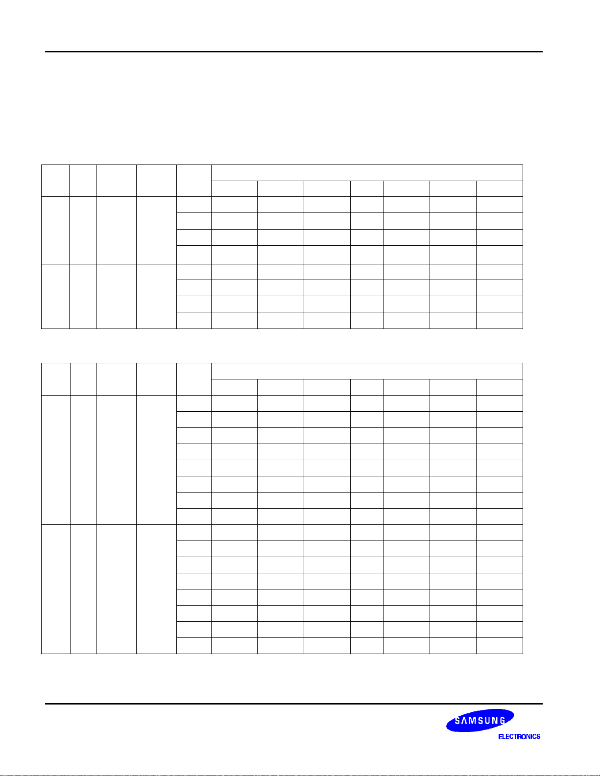
RELATIONSHIP BETWEEN THE DISPLAY DATA AND DRIVER OUTPUT PINS (Table 5)
Segment Mode
(a) 4-bit Parallel Mode
MD L/R EIO1 EIO2
L L Output Input
L H Input Output
(a) 8-bit Parallel Mode
MD L/R EIO1 EIO2
H L Output Input
H H Input Output
Data
Input
DI0 Y157 Y153 Y149 .. Y9 Y5 Y1
DI1 Y158 Y154 Y150 .. Y10 Y6 Y2
DI2 Y159 Y155 Y151 .. Y11 Y7 Y3
DI3 Y160 Y156 Y152 .. Y12 Y8 Y4
DI0 Y4 Y8 Y12 .. Y152 Y156 Y160
DI1 Y3 Y7 Y11 .. Y151 Y155 Y159
DI2 Y2 Y6 Y10 .. Y150 Y154 Y158
DI3 Y1 Y5 Y9 .. Y149 Y153 Y157
Data
Input
DI0 Y153 Y145 Y137 .. Y17 Y9 Y1
DI1 Y154 Y146 Y138 .. Y18 Y10 Y2
DI2 Y155 Y147 Y139 .. Y19 Y11 Y3
DI3 Y156 Y148 Y140 .. Y20 Y12 Y4
DI4 Y157 Y149 Y141 .. Y21 Y13 Y5
DI5 Y158 Y150 Y142 .. Y22 Y14 Y6
DI6 Y159 Y151 Y143 .. Y23 Y15 Y7
DI7 Y160 Y152 Y144 .. Y24 Y16 Y8
DI0 Y8 Y16 Y24 .. Y144 Y152 Y160
DI1 Y7 Y15 Y23 .. Y143 Y151 Y159
DI2 Y6 Y14 Y22 .. Y142 Y150 Y158
DI3 Y5 Y13 Y21 .. Y141 Y149 Y157
DI4 Y4 Y12 Y20 .. Y140 Y148 Y156
DI5 Y3 Y11 Y19 .. Y139 Y147 Y155
DI6 Y2 Y10 Y18 .. Y138 Y146 Y154
DI7 Y1 Y9 Y17 .. Y137 Y145 Y153
1st 2nd 3rd .. 38th 39th 40th
1st 2nd 3rd .. 18th 19th 20th
Figure of clock
Figure of clock
16
Page 17

S6B0794 SPEC. VER 3.0 160 SEG / COM DRIVER FOR STN LCD
Table 5 (Continued)
Common Mode
MD L/R Data transfer direction EIO1 EIO2 DI7
L
(Single)
L(shift to left)
H(shift to right)
Y160 → Y1
Y1 → Y160
Output Input X
Input Output X
L(shift to left)
H
(Dual)
H(shift to right)
Here, L : VSS(0V), H : VDD(+2.4V to +5.5V), X : Don’t care
. Note : “Don’t care” should be fixed to “H” or “L”, avoid floating.
Y160 → Y81
Y80 → Y1
Y1 → Y80
Y81 → Y160
Output Input Input
Input Output Input
17
Page 18

160 SEG / COM DRIVER FOR STN LCD SPEC. VER. 3.0 S6B0794
SPECIFICATIONS
ABSOLUTE MAXIMUM RATINGS
Table 6. Absolute Maximum Ratings
Parameter Symbol Conditions Applicable pins Ratings Unit
Supply voltage (1)
Supply voltage (2)
Input voltage
Storage temperature
VDD VDD -0.3 to +6.5 V
V0 V0L, V0R -0.3 to +35 V
V12 V12L, V12R -0.3 to V0+0.3 V
V43 V43L, V43R -0.3 to V0+0.3 V
V5 V5L, V5R -0.3 to V0+0.3 V
V1
TSTG -45 to 125
Ta=25 °C
Referenced to
VSS(0V)
DI0 –DI7, XCK, LP, L/R,
MD, S/C, EIO1, EIO2,
DISPOFFB
-0.3 to VDD+0.3 V
°C
RECOMMENDED OPERATING CONDITIONS
Table 7. Recommended Operating Conditions
Parameter Symbol Conditions Applicable pins Min. Typ. Max. Unit
Supply voltage (1)
Supply voltage (2)
Operating temperature
Note: Ensure that voltage are set such that VSS≤V5<V43<V12<V0
VDD VDD +2.4 +5.5 V
V0
TOPR -20 +85 °C
Referenced to
VSS(0V)
V0L, V0R +15 +32 V
18
Page 19
S6B0794 SPEC. VER 3.0 160 SEG / COM DRIVER FOR STN LCD
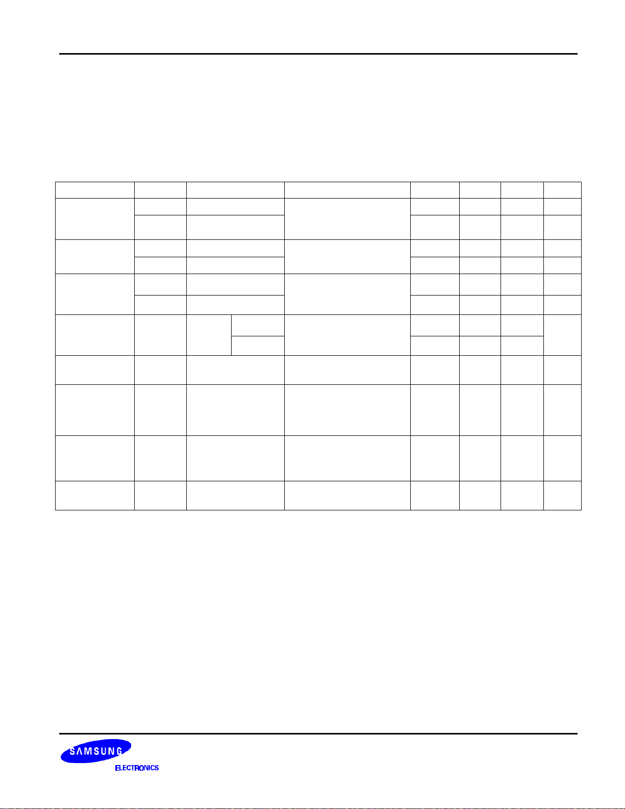
DC CHARACTERISTICS
DC CHARACTERISTICS(Table 8)
Segment Mode
(VSS=V5=0V, VDD=+2.4 to 5.5V, V0=+15 to +32V, Ta=-20~85°C)
Parameter Symbol Conditions Applicable pins Min. Typ. Max. Unit
Input voltage
Output voltage
Input leakage
current
VIH 0.8VDD V
VIL
VOH IOH=-0.4mA VDD-0.4 V
VOL IOL=+0.4mA
ILIH VI=VDD +10 uA
ILIL VI=VSS
DI0 -DI7, XCK, LP, L/R,
FR, MD, S/C,EIO1, EIO2,
DISPOFFB
EIO1, EIO2
DI0 -DI7, XCK, LP, L/R,
FR, MD, S/C,EIO1, EIO2,
DISPOFFB
0.2VDD V
+0.4 V
-10 uA
Output
resistance
Stand-by
current
Consumed
current(1)
(Deselection)
Consumed
current(2)
(Selection)
Consumed
current
RON
ISTB *1 VSS 50.0 uA
IDD1 *2 VDD 2.0 mA
IDD2 *3 VDD 8.0 mA
I0 *4 V0 1.0 mA
|∆VON|
=0.5V
V0=+30V 1.0 1.5
V0=+20V
Y1- Y160
1.5 2.0
NOTE : *1 VDD=+5V, V0=+32V, VI=VSS
*2 VDD=+5V, V0=+32V, fXCK=14MHz, No-load, EI=VDD
The input data is turned over by data taking clock (4-bit parallel input mode)
*3 VDD=+5V, V0=+32V, fXCK=14MHz, No-load, EI=VSS
The input data is turned over by data taking clock (4-bit parallel input mode)
*4 VDD=+5V, V0=+32V, fXCK=14MHz, fLP=25.6kHz, fFR=80Hz, No-load
The input data is turned over by data taking clock (4-bit parallel input mode)
kΩ
19
Page 20

160 SEG / COM DRIVER FOR STN LCD SPEC. VER. 3.0 S6B0794
Table 8 (Continued)
Common Mode
(VSS=V5=0V, VDD=+2.4 to 5.5V, V0=+15 to +32V, Ta=-20~85°C)
Parameter Symbol Conditions Applicable pins Min. Typ. Max. Unit
Input voltage
Output voltage
Input leakage
current
VIH 0.8VDD V
VIL
VOH IOH=-0.4mA VDD-0.4 V
VOL IOL=+0.4mA
ILIH VI=VDD +10 uA
ILIL VI=VSS
DI0 -DI7, XCK, LP, L/R,
FR, MD, S/C,EIO1, EIO2,
DISPOFFB
EIO1, EIO2
DI0 -DI7, XCK, LP, L/R,
FR, MD, S/C,EIO1, EIO2,
DISPOFFB
0.2VDD V
+0.4 V
-10 uA
Output
resistance
Input pull-
down current
Stand-by
current
Consumed
current(1)
Consumed
current(2)
RON
|∆VON|
=0.5V
IPD VI=VDD XCK, EIO1, EIO2, DI7 100.0 uA
ISTB *1 VSS 50.0 uA
IDD *2 VDD 80.0 uA
I0 *2 V0 160.0 uA
V0=+30V 1.0 1.5
V0=+20V
NOTE : *1 VDD=+5V, V0=+32V, VI=VSS
*2 VDD=+5V, V0=+32V, fLP=25.6kHz, fFR=80Hz
case of 1/320 duty operation, No-load
Y1 - Y160
kΩ
1.5 2.0
20
Page 21
S6B0794 SPEC. VER 3.0 160 SEG / COM DRIVER FOR STN LCD
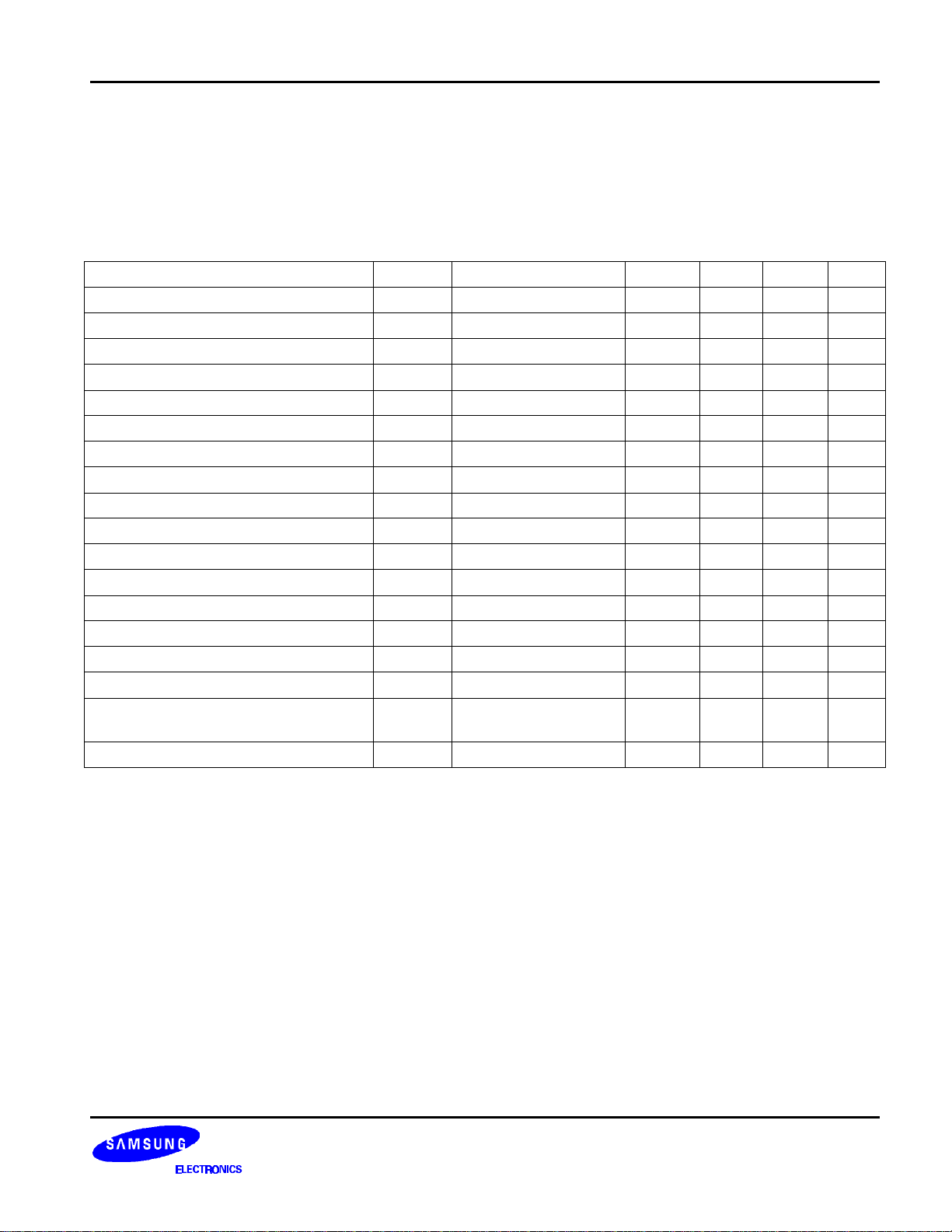
AC CHARACTERISTICS
SEGMENT MODE AC CHARACTERISTICS (Table 9)
Segment Mode 1
(VSS=V5=0V, VDD=+4.5 to +5.5V, V0=+15 to +32V, Ta=-20~85°C)
Parameter Symbol Conditions Min. Typ. Max. Unit
Shift clock period *1 TWCK
Shift clock “H” pulse width TWCKH 23 ns
Shift clock “L” pulse width TWCKL 23 ns
Data setup time TDS 10 ns
Data hold time TDH 20 ns
Latch pulse “H” pulse width TWLPH 23 ns
Shift clock rise to latch pulse rise time TLD 0 ns
Shift clock fall to latch pulse fall time TSL 25 ns
Latch pulse rise to shift clock rise time TLS 25 ns
Latch pulse fall to shift clock fall time TLH 25 ns
Input signal rise time *2 TR 50 ns
Input signal fall time *2 TF 50 ns
Enable setup time TS 21 ns
DISPOFFB removal time TSD 100 ns
DISPOFFB “L” pulse width TWDL 1.2 us
Output delay time (1) TD CL=15pF 40 ns
Output delay time (2)
Output delay time (3) TPD3 CL=15pF 1.2 us
Note : *1 Take the cascade connection into consideration.
TPD1,
TPD2
TR, TF≤10 ns
CL=15pF 1.2 us
71 ns
*2 (TWCK – TWCKH – TWCKL) / 2 is maximum in the case of high speed operation.
21
Page 22
160 SEG / COM DRIVER FOR STN LCD SPEC. VER. 3.0 S6B0794
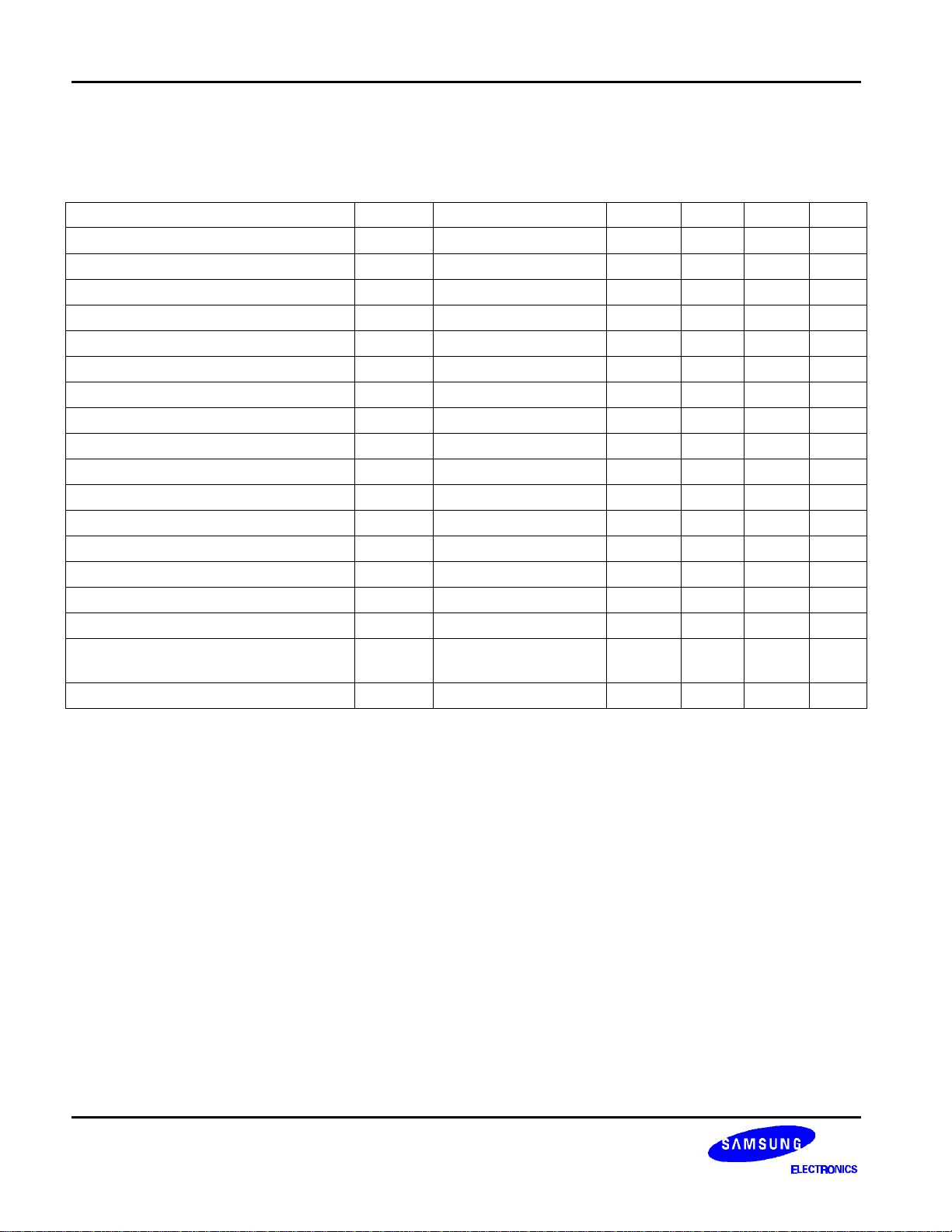
Table 9 (Continued)
Segment Mode 2
(VSS=V5=0V, VDD=+2.4V to +4.5V, V0=+15 to +32V, Ta=-20~85°C)
Parameter Symbol Conditions Min. Typ. Max. Unit
Shift clock period *1 TWCK
Shift clock “H” pulse width TWCKH 51 ns
Shift clock “L” pulse width TWCKL 51 ns
Data setup time TDS 30 ns
Data hold time TDH 40 ns
Latch pulse “H” pulse width TWLPH 51 ns
Shift clock rise to latch pulse rise time TLD 0 ns
Shift clock fall to latch pulse fall time TSL 51 ns
Latch pulse rise to shift clock rise time TLS 51 ns
Latch pulse fall to shift clock fall time TLH 51 ns
Input signal rise time *2 TR 50 ns
Input signal fall time *2 TF 50 ns
Enable setup time TS 36 ns
DISPOFFB removal time TSD 100 ns
DISPOFFB “L” pulse width TWDL 1.2 us
Output delay time (1) TD CL=15pF 78 ns
Output delay time (2)
Output delay time (3) TPD3 CL=15pF 1.2 us
Note : *1 Take the cascade connection into consideration.
TPD1,
TPD2
TR, TF≤10 ns
CL=15pF 1.2 us
125 ns
*2 (TWCK – TWCKH – TWCKL) / 2 is maximum in the case of high speed operation.
22
Page 23
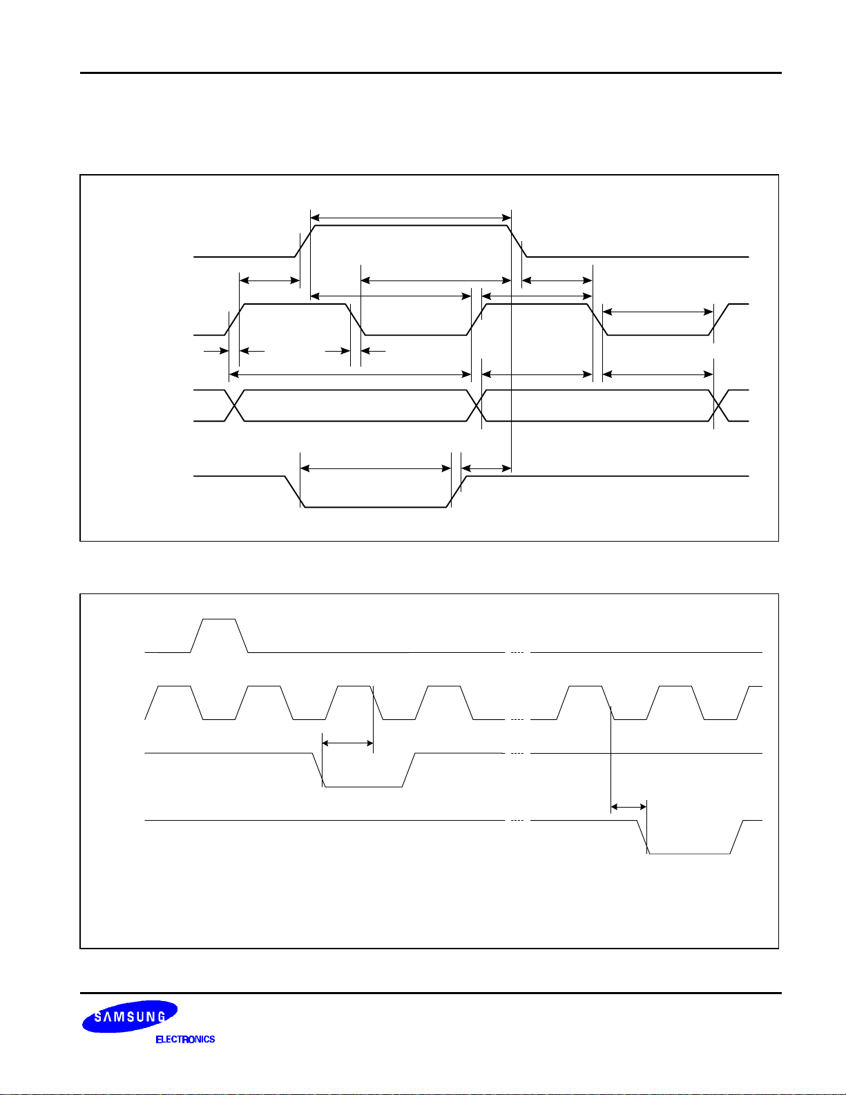
S6B0794 SPEC. VER 3.0 160 SEG / COM DRIVER FOR STN LCD
Timing Characteristics of Segment Mode (Figure 3)
T
WLPH
LP
T
T
LD
SL
T
LS
T
WCKH
T
LH
T
WCKL
XCK
T
R
T
F
T
T
T
WCK
DS
DH
DI0 - DI
DISPOFFB
LP
XCK
EI
7
LAST DATA TOP DATA
T
WDL
T
SD
(*)
1
T
S
2
n
T
D
EO
(*) n : 4 - bit parallel mode 40
8 - bit parallel mode 20
23
Page 24
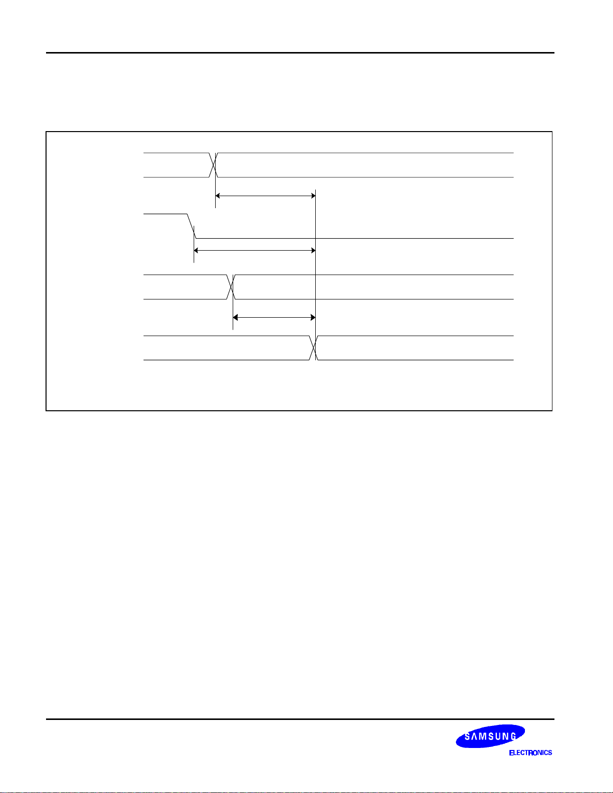
160 SEG / COM DRIVER FOR STN LCD SPEC. VER. 3.0 S6B0794
Figure 3. (Continued)
FR
T
PD1
LP
T
PD2
DISPOFFB
PD3
T
Y1 ~Y
160
[L/R="L"]
24
Page 25

S6B0794 SPEC. VER 3.0 160 SEG / COM DRIVER FOR STN LCD
COMMON MODE AC CHARACTERISTICS (Table 10)
Common Mode
(VSS=V5=0V, VDD=+2.4V to +4.5V, V0=+15 to +32V, Ta=-20~85°C)
Parameter Symbol Condition Min. Typ. Max. Unit
Shift clock period
Shift “H” pulse width
Data setup time
Data hold time
Input signal rise time
Input signal fall time
DISPOFFB removal time
DISPOFFB ‘L” pulse width
Output delay time (1)
Output delay time (2)
Output delay time (3)
TWLP
TR, TF≤20ns
VDD=+5.0V±10%
250 ns
15 ns
TWLPH
VDD=+2.5V~+4.5V 30 ns
TSU 30 ns
TH 50 ns
TR 50 ns
TF 50 ns
TSD 100 ns
TWDL 1.2 us
TDL CL=15pF 200 ns
TPD1,TPD2 CL=15pF 1.2 us
TPD3 CL=15pF 1.2 us
Timing Characteristics of Common Mode (Figure 4)
LP
T
EIO
R
2
T
WLPH
T
SU
T
T
(DI7)
EIO
1
DISPOFFB
T
WLP
F
H
T
DL
T
T
WDL
SD
25
Page 26
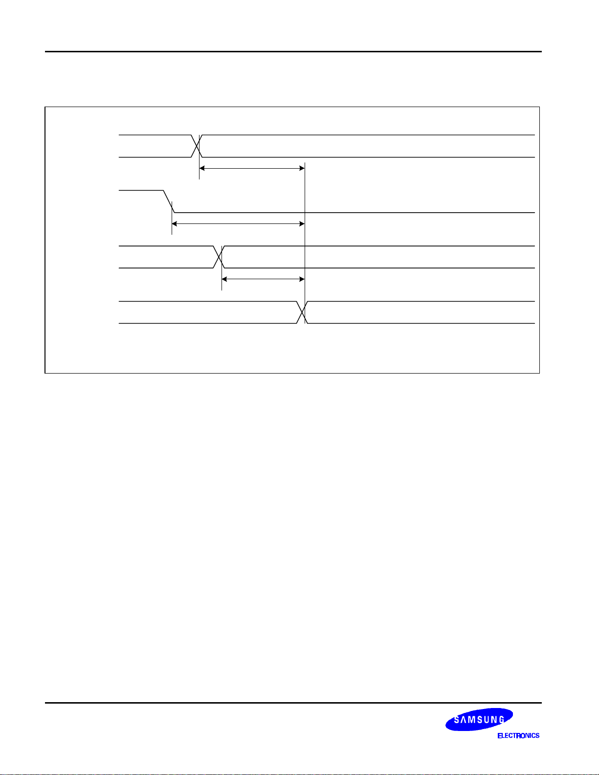
160 SEG / COM DRIVER FOR STN LCD SPEC. VER. 3.0 S6B0794
Figure 4. (Continued)
FR
TPD1
LP
TPD2
DISPOFFB
TPD3
Y1~ Y160
[L/R="L"]
26
Page 27

S6B0794 SPEC. VER 3.0 160 SEG / COM DRIVER FOR STN LCD
PRECAUTION
. PRECAUTION WHEN CONNECTING OR DISCONNECTING THE POWER
This LSI has a high-voltage LC driver, so it may be permanently damaged by a high current
which may flow if a voltage is supplied to the LC driver power supply while the logic system
power supply is floating. The detail is as follows.
. When connecting the power supply, connect the LC drive power after connecting the logic
system power. Furthermore, when disconnecting the power, disconnect the logic system
power after disconnecting the LC driver power.
. We recommend you connecting the serial resistor (50~100Ω) or fuse to the LC drive power
V0 of the system as a current limiter. And set up the suitable of the resistor in consideration of
LC display grade.
And when connecting the logic power supply, the logic condition of this LSI inside is
insecurity. Therefore connect the LC driver power supply after resetting logic condition of this
LSI inside on DISPOFFB function. After that, cancel the DISPOFFB function after the LC
driver power supply has become stable. Furthermore, when disconnecting the power, set the
LC drive output pins to level V5 on DISPOFFB function. After that, disconnect the logic
system power after disconnecting the LC drive power. When connecting the power supply,
show the following recommend sequence.
V
DD
V
DD
V
SS
V
DD
DISPOFFB
V
SS
V
0
V
0
V
SS
Figure 5.
27
Page 28

160 SEG / COM DRIVER FOR STN LCD SPEC. VER. 3.0 S6B0794
CONNECTION EXAMPLES OF PLURAL SEGMENT DRIVERS
(a) CASE OF L/R = "L"
XCK
DIO
-
VSS
DIO
-
top
data
Y160
2
EIO
X
LPMDF
C
K
LP
MD
FR
0
DIO
7
(b) CASE OF L/R = "H"
VDD
0
DIO
7
FR
MD
LP
XCK
last
data
Y1
EIO
1
Y160
EIO
2
L/R
D
D
I
I
O
O
7
0
R
X
C
K
LPMDF
Y1
EIO
1
Y160
EIO
2
L/R
D
D
I
I
O
O
7
0
R
X
C
K
LPMDF
Y1
EIO
1
L/R
D
D
I
I
O
O
7
0
R
8
8
28
VSS
EIO
Y1
X
C
K
1
top
data
LPMDF
X
D
D
R
I
I
O
O
7
0
LPMDF
C
K
L/R
EIO
EIO
Y160
2
1
Y1
D
D
R
I
I
O
O
7
0
L/R
EIO
2
Y160
X
C
K
EIO
Y1
LPMDF
1
D
D
R
I
I
O
O
7
0
L/R
EIO
2
Y160
last
data
Figure 6.
Page 29
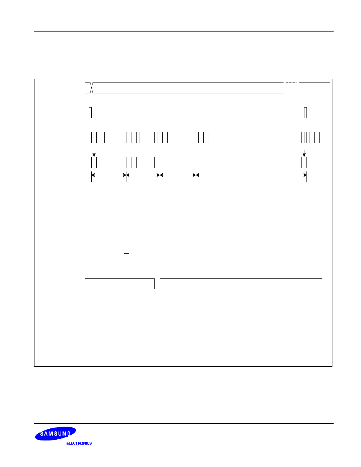
S6B0794 SPEC. VER 3.0 160 SEG / COM DRIVER FOR STN LCD
TIMING CHART OF 4-DEVICE CASECADE CONNECTION OF SEGMENT
DRIVERS
FR
LP
XCK
TOP DATA
DI0-DI
7
n 1 2 n 1 2 n 1 2 n 1 2 n 1 2
device A device B
EI
(device A)
EO
(device A)
EO
(device B)
EO
(device C)
(*)
device C
LAST DATA
device D
Low
(*) n:4-bit parallel mode 40
8-bit parallel mode 20
Figure 7.
29
Page 30

160 SEG / COM DRIVER FOR STN LCD SPEC. VER. 3.0 S6B0794
CONNECTION EXAMPLES OF PLURAL COMMON DRIVERS
(a) SINGLE MODE(SHIFTING TOWARD LEFT)
VSS
(VDD)
LP
VSS
FR
DISPOFFB
VSS
DISPOFFB
first
Y1
EIO
1
L/R
D
I
S
P
O
F
F
B
R
Y160
EIO
D
I
7
DI
Y160
EIO
2
D
I
7
LPMDF
(b) SINGLE MODE(SHIFTING TOWARD RIGHT)
VDD
FR
VSS
LP
VSS
(VDD)
D
I
R
S
P
O
F
F
B
L/R
EIO
2
Y160
EIO
Y1
D
I
7
DI
EIO
Y1
D
I
7
1
LPMDF
2
LPMDF
LPMDF
1
last
Y1
EIO
1
L/R
D
I
S
P
O
F
F
B
R
D
I
R
S
P
O
F
F
B
L/R
EIO
2
Y160
Y160
EIO
D
I
7
EIO
Y1
2
D
I
7
LPMDF
LPMDF
1
Y1
EIO
1
L/R
D
I
S
P
O
F
F
B
R
D
I
R
S
P
O
F
F
B
L/R
EIO
2
Y160
30
first
last
Figure 8.
Page 31
S6B0794 SPEC. VER 3.0 160 SEG / COM DRIVER FOR STN LCD
(c)DUAL MODE(SHIFTING TOWARD LEFT)
DI1
VSS
(VDD)
LP
VSS
FR
DISPOFFB
VDD
VSS
DI2
DI2
VDD
VDD
DISPOFFB
FR
VSS
(VDD)
DI1
first1
Y160
EIO
2
D
I
7
LPMDF
Y1
EIO
1
L/R
D
I
S
P
O
F
F
B
R
(d)DUAL MODE(SHIFTING TOWARD RIGHT)
LP
VSS
D
I
R
S
P
O
F
F
B
L/R
EIO
2
Y160
EIO
Y1
D
I
7
LPMDF
1
last1 first2 last2
Y160
EIO
D
7
EIO
Y1
2
I
D
I
7
Y81 Y80
LPMDF
LPMDF
1
Y80
Y81
Y1
EIO
1
L/R
D
I
S
P
O
F
F
B
R
D
I
R
S
P
O
F
F
B
L/R
EIO
2
Y160
Y160
EIO
EIO
Y1
D
I
7
D
I
7
2
LPMDF
LPMDF
1
Y1
EIO
1
L/R
D
I
S
P
O
F
F
B
R
D
I
R
S
P
O
F
F
B
L/R
EIO
2
Y160
first1
last1 first2
Figure 9.
last2
31
 Loading...