

Page 1

S6B0741
permission of LCD Driver IC Team.
128 SEG / 129 COM DRIVER & CONTROLLER FOR 4 GRAY SCALE STN LCD
Contents in this document are subject to change without notice. No part of this document may be reproduced or
transmitted in any form or by any means, electronic or mechanical, for any purpose, without the express written
August 6. 2000.
Ver. 2.1
Prepared by: Hyung-Suk, Kim
Page 2

128 SEG / 129 COM DRIVER & CONTROLLER FOR STN LCD S6B0741
S6B0741 Specification Revision History
Version Content Date
0.0 Preliminary specification (short form) June 8, 1999
0.1 Preliminary specification (full set) July 14, 1999
0.2 Added temporary pin number (page 5,6) July 15, 1999
Removed HPMB, CS2 pins
0.3
CS1B pin → CSB pin
July 30, 1999
VOL Max.: 0.3VDD → 0.2VDD , VOH Min.: 0.7VDD → 0.8VDD (page 59)
Removed CLS, OSCCK, OSC2 pins (page 7,8)
0.4
Read internal status: MF, DS ID is added, ADC is removed (Page 35, 39)
RESET flag: 0: display ON, 1: display OFF
Aug. 12, 1999
→ 0: display OFF, 1: display ON (Page 39)
Changed input pin order, add RESETB pin (page 5)
Added VR, VEXT pin connection (page 8)
VR: When using internal resistors (INTRS = "H"), open this pin
VEXT: When using internal voltage regulator, connect to VDD, VSS or open this pin
0.5
Added test pin connection (page 9)
Aug. 30, 1999
TEST1,TEST2: connect to “VDD”
TEST3,TEST4,TEST5: connect to “VSS”
Changed OSC resistance connection (page8, 23)
Between OSC1 and OSC2 → between OSC1 and VDD
Removed TEST2, TEST3, TEST4, TEST5, TEST6, TEST7 pins
0.6
Added COMS, COMS1 for ICON display.
Sep. 30, 1999
Added ICON control register ON/OFF instruction.
0.7
Removed COMS, COMS1 for ICON display.
Removed ICON control register ON/OFF instruction.
Oct. 4, 1999
Added COMS, COMS1 for ICON display.
Added ICON control register ON/OFF instruction.
1.0
Modified bit settings for partial display command.
Jan. 18, 2000
Relaxed VIH and VIL specifications.
Modified interface timing specs.
Added 6800-mode interface description for data latch with CSB (page 14)
C2 CAP value : 0.1 to 0.47uF → 0.47 to 2.0uF (page 34)
Added Icon Mode Disabled to the Reset default list. (page 36)
1.1
Added description of the column address operation. (page 40)
Added that Display On/Off command has priority over Entire Display On/Off and
Jan. 24, 2000
Reverse Display On/Off. (page 44)
Added N-line inversion command description (page 47)
The lower limit of VOUT, V0 - V4 : +0.3V → -0.3V (page 60)
1.2 The upper limit of V1 - V4 : V0 → V0 + 0.3V (page 60) Feb. 8, 2000
2
Page 3

S6B0741 128 SEG / 129 COM DRIVER & CONTROLLER FOR STN LCD
S6B0741 Specification Revision History (Continued)
Version Content Date
Changed temperature coefficient value (page 1)
2.0
Determined current consumption (page 2, 62)
Added remarks about oscillator resistor (page 61, 63)
Jun. 26, 2000
Changed parallel interface timing (page 17, 64, 65)
2.1 Removed wrong description about display data ram. (page 1) Aug. 6, 2000
3
Page 4

128 SEG / 129 COM DRIVER & CONTROLLER FOR STN LCD S6B0741
CO
NTENTS
INTRODUCTION..................................................................................................................................................1
FEATURES .........................................................................................................................................................1
BLOCK DIAGRAM ..............................................................................................................................................3
PAD CONFIGURATION.......................................................................................................................................4
PAD Center Coordinates.................................................................................................................................... 6
PIN DESCRIPTION.............................................................................................................................................. 6
POWER SUPPLY.........................................................................................................................................9
LCD DRIVER SUPPLY................................................................................................................................. 9
SYSTEM CONTROL................................................................................................................................... 10
MICROPROCESSOR INTERFACE ............................................................................................................ 11
LCD DRIVER OUTPUTS............................................................................................................................ 13
FUNCTIONAL DESCRIPTION........................................................................................................................... 14
MICROPROCESSOR INTERFACE ............................................................................................................ 14
DISPLAY DATA RAM (DDRAM)................................................................................................................. 18
LCD DISPLAY CIRCUITS ........................................................................................................................... 21
LCD DRIVER CIRCUIT............................................................................................................................... 26
POWER SUPPLY CIRCUITS...................................................................................................................... 29
REFERECE CIRCUIT EXAMPLES............................................................................................................. 34
RESET CIRCUIT........................................................................................................................................ 36
INSTRUCTION DESCRIPTION.......................................................................................................................... 37
SPECIFICATIONS............................................................................................................................................. 60
ABSOLUTE MAXIMUM RATINGS.............................................................................................................. 60
DC CHARACTERISTICS............................................................................................................................ 61
AC CHARACTERISTICS............................................................................................................................ 64
REFERENCE APPLICATIONS.......................................................................................................................... 68
MICROPROCESSOR INTERFACE ............................................................................................................ 68
CONNECTIONS BETWEEN S6B0741 AND LCD PANEL........................................................................... 70
4
Page 5

S6B0741 128 SEG / 129 COM DRIVER & CONTROLLER FOR STN LCD
INTRODUCTION
The S6B0741 is a driver & controller LSI for 4-level gray scale graphic dot-matrix liquid crystal display systems. It
contains 128 segment and 129 common driver circuits. This chip is connected directly to a microprocessor, accepts
Serial Peripheral Interface (SPI) or 8-bit parallel display data and stores in an on-chip display data RAM of 128 x 129
x 2 bits. It performs display data RAM read/write operation with no external operating clock to minimize power
consumption. In addition, because it contains power supply circuits necessary to drive liquid crystal, it is possible to
make a display system with the fewest components.
FEATURES
4-level (White, Light Gray, Dark Gray, Black) Gray Scale Display with PWM and FRC Methods
DDRAM data [2n: 2n+1] 00 01 10 11
Gray scale White Light gray Dark gray Dark
(Accessible column address, n = 0, 1, 2, ……, 125, 126, 127)
Driver Output Circuits
− 128 segment outputs / 129 common outputs
Applicable Duty Ratios
Duty ratio Applicable LCD bias Maximum display area
1/16 ~ 1/128 (ICON disabled)
1/17 ~ 1/129 (ICON enabled)
− Various partial display
− Partial window moving & data scrolling
On-chip Display Data RAM
− Capacity: 129 × 128 × 2 = 33,024bits
Microprocessor Interface
− 8-bit parallel bi-directional interface with 6800-series or 8080-series
− SPI (serial peripheral interface) available (only write operation)
On-chip Low Power Analog Circuit
− On-chip oscillator circuit
− Voltage converter (x3, x4, ×5 or x6)
− Voltage regulator (temperature coefficient: -0.125%/°C, or external input)
− On-chip electronic contrast control function (64 steps)
− Voltage follower (LCD bias : 1/5 to 1/12)
Operating Voltage Range
− Supply voltage (VDD): 1.8 to 3.3V
− LCD driving voltage (VLCD = V0 - VSS): 4.0 to 15.0 V
1/5 to 1/12 129 × 128
1
Page 6

128 SEG / 129 COM DRIVER & CONTROLLER FOR STN LCD S6B0741
Low Power Consumption
− 300 µΑ Max. (operation)
− 2 µΑ Max. (sleep mode)
Package Type
− Slim chip for TCP
2
Page 7

S6B0741 128 SEG / 129 COM DRIVER & CONTROLLER FOR STN LCD
DB0
DB1
COMS1
COM127
COM126
TEST1
BLOCK DIAGRAM
SEG127
SEG126
VDD
V0
V1
V2
V3
V4
VSS
SEG2
SEG1
SEG0
128 SEGMENT
DRIVER CIRCUITS
SEG125
:
COMS
COM1
COM0
DRIVER CIRCUITS
:
129 COMMON
V0
VR
INTRS
VEXT
REF
VOUT
C1-
C1+
C2C2+
C3+
C4+
C5+
VCl
V / F
CIRCUIT
V / R
CIRCUIT
V / C
CIRCUIT
INTERNAL
POWER
SUPPLY
PAGE
ADDRESS
CIRCUIT
I/O
BUFFER
DISPLAY LATCH CIRCUIT
FRC/PWM FUNCTION CIRCUIT
DISPLAY DATA RAM
129 X 128 X 2 = 33,024 Bits
COLUMN ADDRESS
CIRCUIT
STATUS REGISTER INSTRUCTION REGISTER
LINE
ADDRESS
CIRCUIT
INSTRUCTION DECODERBUS HOLDER
COMMON
OUTPUT
CONTROLLER
CIRCUIT
OSCILLATOR
/DISPLAY
TIMING
CONTROL
OSC1
MPU INTERFACE (PARALLEL & SERIAL)
DB4
DB5
DB6(SCLK)
DB7(SID)
RW_WR
E_RD
RS
CSB
PS0
PS1
RESETB
Figure 1. Block Diagram
DB3
DB2
3
Page 8

128 SEG / 129 COM DRIVER & CONTROLLER FOR STN LCD S6B0741
…..
…..
S6B0741
PAD CONFIGURATION
.......................
375
374
Y
181
180
(0,0)
X
411
1 143
............
PAD
Figure 2. S6B0741 Chip Configuration
Table 1. S6B0741 Pad Dimensions
ITEM PAD NO.
Chip Size - 10580 2520
1 ~ 143 70
144 ~ 178
Pad Pitch
Bumped pad size
Bumped pad height ALL PAD 14 (TYP)
183 ~ 372
377 ~ 411
179 ~ 182
373 ~ 376
1 ~ 143 42 92
145 ~ 178
377 ~ 410
183 ~ 372 34 70
144
179 ~ 180
375 ~ 376
411
181 ~ 182
373 ~ 374
SIZE
X Y
52
80
70 34
70 62
62 70
144
UNIT
§-
4
Page 9

S6B0741 128 SEG / 129 COM DRIVER & CONTROLLER FOR STN LCD
(+4527, +624.5)
(-4690, -515)
30µm
30µm
30µm
60
µ
m
30
µ
m
42µm
108µm
42µm
108µm
(-4607, +704.5)
(+4770, -580)
COG Align Key Coordinate ILB Align Key Coordinate
30µm 30µm 30µm
30µm 30µm 30µm
42µm 108µm
42µm108µm
5
Page 10

128 SEG / 129 COM DRIVER & CONTROLLER FOR STN LCD S6B0741
PAD CENTER COORDINATES
Table 2. Pad Center Coordinates
[Unit: µm]
NO. Name X Y NO. Name X Y NO. Name X Y NO. Name X Y
1 DUMMY -4970 -1145 51 DUMMY -1470 -1145 101 C3+ 2030 -1145 151 COM57 5166 -586
2 DUMMY -4900 -1145 52 DUMMY -1400 -1145 102 C3+ 2100 -1145 152 COM56 5166 -534
3 DUMMY -4830 -1145 53 DUMMY -1330 -1145 103 C1- 2170 -1145 153 COM55 5166 -482
4 DUMMY -4760 -1145 54 DUMMY -1260 -1145 104 C1- 2240 -1145 154 COM54 5166 -430
5 DUMMY -4690 -1145 55 DUMMY -1190 -1145 105 C1+ 2310 -1145 155 COM53 5166 -378
6 DUMMY -4620 -1145 56 DUMMY -1120 -1145 106 C1+ 2380 -1145 156 COM52 5166 -326
7 DUMMY -4550 -1145 57 DUMMY -1050 -1145 107 C2+ 2450 -1145 157 COM51 5166 -274
8 DUMMY -4480 -1145 58 DUMMY -980 -1145 108 C2+ 2520 -1145 158 COM50 5166 -222
9 DUMMY -4410 -1145 59 VDD -910 -1145 109 C2- 2590 -1145 159 COM49 5166 -170
10 DUMMY -4340 -1145 60 TEST1 -840 -1145 110 C2- 2660 -1145 160 COM48 5166 -118
11 DUMMY -4270 -1145 61 VSS -770 -1145 111 C4+ 2730 -1145 161 COM47 5166 -66
12 DUMMY -4200 -1145 62 PS0 -700 -1145 112 C4+ 2800 -1145 162 COM46 5166 -14
13 DUMMY -4130 -1145 63 VDD -630 -1145 113 VDD 2870 -1145 163 COM45 5166 38
14 DUMMY -4060 -1145 64 PS1 -560 -1145 114 VDD 2940 -1145 164 COM44 5166 90
15 DUMMY -3990 -1145 65 VSS -490 -1145 115 REF 3010 -1145 165 COM43 5166 142
16 DUMMY -3920 -1145 66 CSB -420 -1145 116 VSS 3080 -1145 166 COM42 5166 194
17 DUMMY -3850 -1145 67 RESETB -350 -1145 117 VEXT 3150 -1145 167 COM41 5166 246
18 DUMMY -3780 -1145 68 VDD -280 -1145 118 VDD 3220 -1145 168 COM40 5166 298
19 DUMMY -3710 -1145 69 RS -210 -1145 119 INTRS 3290 -1145 169 COM39 5166 350
20 DUMMY -3640 -1145 70 RW_WR -140 -1145 120 VSS 3360 -1145 170 COM38 5166 402
21 DUMMY -3570 -1145 71 VSS -70 -1145 121 VSS 3430 -1145 171 COM37 5166 454
22 DUMMY -3500 -1145 72 E_RD 0 -1145 122 V4 3500 -1145 172 COM36 5166 506
23 DUMMY -3430 -1145 73 VDD 70 -1145 123 V4 3570 -1145 173 COM35 5166 558
24 DUMMY -3360 -1145 74 DB0 140 -1145 124 V3 3640 -1145 174 COM34 5166 610
25 DUMMY -3290 -1145 75 DB1 210 -1145 125 V3 3710 -1145 175 COM33 5166 662
26 DUMMY -3220 -1145 76 DB2 280 -1145 126 V2 3780 -1145 176 COM32 5166 714
27 DUMMY -3150 -1145 77 DB3 350 -1145 127 V2 3850 -1145 177 COM31 5166 766
28 DUMMY -3080 -1145 78 DB4 420 -1145 128 V1 3920 -1145 178 COM30 5166 818
29 DUMMY -3010 -1145 79 DB5 490 -1145 129 V1 3990 -1145 179 DUMMY 5166 884
30 DUMMY -2940 -1145 80 DB6 560 -1145 130 V0 4060 -1145 180 DUMMY 5166 964
31 DUMMY -2870 -1145 81 DB7 630 -1145 131 V0 4130 -1145 181 DUMMY 5060 1136
32 DUMMY -2800 -1145 82 VDD 700 -1145 132 VR 4200 -1145 182 DUMMY 4980 1136
33 DUMMY -2730 -1145 83 VDD 770 -1145 133 VR 4270 -1145 183 COM29 4914 1136
34 DUMMY -2660 -1145 84 VDD 840 -1145 134 VSS 4340 -1145 184 COM28 4862 1136
35 DUMMY -2590 -1145 85 VDD 910 -1145 135 VSS 4410 -1145 185 COM27 4810 1136
36 DUMMY -2520 -1145 86 VDD 980 -1145 136 VDD 4480 -1145 186 COM26 4758 1136
37 DUMMY -2450 -1145 87 VDD 1050 -1145 137 OSC1 4550 -1145 187 COM25 4706 1136
38 DUMMY -2380 -1145 88 VCI 1120 -1145 138 DUMMY 4620 -1145 188 COM24 4654 1136
39 DUMMY -2310 -1145 89 VCI 1190 -1145 139 DUMMY 4690 -1145 189 COM23 4602 1136
40 DUMMY -2240 -1145 90 VSS 1260 -1145 140 DUMMY 4760 -1145 190 COM22 4550 1136
41 DUMMY -2170 -1145 91 VSS 1330 -1145 141 DUMMY 4830 -1145 191 COM21 4498 1136
42 DUMMY -2100 -1145 92 VSS 1400 -1145 142 DUMMY 4900 -1145 192 COM20 4446 1136
43 DUMMY -2030 -1145 93 VSS 1470 -1145 143 DUMMY 4970 -1145 193 COM19 4394 1136
44 DUMMY -1960 -1145 94 VSS 1540 -1145 144 DUMMY 5166 -964 194 COM18 4342 1136
45 DUMMY -1890 -1145 95 VSS 1610 -1145 145 COM63 5166 -898 195 COM17 4290 1136
46 DUMMY -1820 -1145 96 VSS 1680 -1145 146 COM62 5166 -846 196 COM16 4238 1136
47 DUMMY -1750 -1145 97 VOUT 1750 -1145 147 COM61 5166 -794 197 COM15 4186 1136
48 DUMMY -1680 -1145 98 VOUT 1820 -1145 148 COM60 5166 -742 198 COM14 4134 1136
49 DUMMY -1610 -1145 99 C5+ 1890 -1145 149 COM59 5166 -690 199 COM13 4082 1136
50 DUMMY -1540 -1145 100 C5+ 1960 -1145 150 COM58 5166 -638 200 COM12 4030 1136
6
Page 11

S6B0741 128 SEG / 129 COM DRIVER & CONTROLLER FOR STN LCD
Table 2. PAD Center Coordinates (Continued)
[unit: µm ]
NO. Name X Y NO. Name X Y NO. Name X Y NO. Name X Y
201 COM11 3978 1136 251 SEG37 1378 1136 301 SEG87 -1222 1136 351 COM73 -3822 1136
202 COM10 3926 1136 252 SEG38 1326 1136 302 SEG88 -1274 1136 352 COM74 -3874 1136
203 COM9 3874 1136 253 SEG39 1274 1136 303 SEG89 -1326 1136 353 COM75 -3926 1136
204 COM8 3822 1136 254 SEG40 1222 1136 304 SEG90 -1378 1136 354 COM76 -3978 1136
205 COM7 3770 1136 255 SEG41 1170 1136 305 SEG91 -1430 1136 355 COM77 -4030 1136
206 COM6 3718 1136 256 SEG42 1118 1136 306 SEG92 -1482 1136 356 COM78 -4082 1136
207 COM5 3666 1136 257 SEG43 1066 1136 307 SEG93 -1534 1136 357 COM79 -4134 1136
208 COM4 3614 1136 258 SEG44 1014 1136 308 SEG94 -1586 1136 358 COM80 -4186 1136
209 COM3 3562 1136 259 SEG45 962 1136 309 SEG95 -1638 1136 359 COM81 -4238 1136
210 COM2 3510 1136 260 SEG46 910 1136 310 SEG96 -1690 1136 360 COM82 -4290 1136
211 COM1 3458 1136 261 SEG47 858 1136 311 SEG97 -1742 1136 361 COM83 -4342 1136
212 COM0 3406 1136 262 SEG48 806 1136 312 SEG98 -1794 1136 362 COM84 -4394 1136
213 COMS 3354 1136 263 SEG49 754 1136 313 SEG99 -1846 1136 363 COM85 -4446 1136
214 SEG0 3302 1136 264 SEG50 702 1136 314 SEG100 -1898 1136 364 COM86 -4498 1136
215 SEG1 3250 1136 265 SEG51 650 1136 315 SEG101 -1950 1136 365 COM87 -4550 1136
216 SEG2 3198 1136 266 SEG52 598 1136 316 SEG102 -2002 1136 366 COM88 -4602 1136
217 SEG3 3146 1136 267 SEG53 546 1136 317 SEG103 -2054 1136 367 COM89 -4654 1136
218 SEG4 3094 1136 268 SEG54 494 1136 318 SEG104 -2106 1136 368 COM90 -4706 1136
219 SEG5 3042 1136 269 SEG55 442 1136 319 SEG105 -2158 1136 369 COM91 -4758 1136
220 SEG6 2990 1136 270 SEG56 390 1136 320 SEG106 -2210 1136 370 COM92 -4810 1136
221 SEG7 2938 1136 271 SEG57 338 1136 321 SEG107 -2262 1136 371 COM93 -4862 1136
222 SEG8 2886 1136 272 SEG58 286 1136 322 SEG108 -2314 1136 372 COM94 -4914 1136
223 SEG9 2834 1136 273 SEG59 234 1136 323 SEG109 -2366 1136 373 DUMMY -4980 1136
224 SEG10 2782 1136 274 SEG60 182 1136 324 SEG110 -2418 1136 374 DUMMY -5060 1136
225 SEG11 2730 1136 275 SEG61 130 1136 325 SEG111 -2470 1136 375 DUMMY -5166 964
226 SEG12 2678 1136 276 SEG62 78 1136 326 SEG112 -2522 1136 376 DUMMY -5166 884
227 SEG13 2626 1136 277 SEG63 26 1136 327 SEG113 -2574 1136 377 COM95 -5166 818
228 SEG14 2574 1136 278 SEG64 -26 1136 328 SEG114 -2626 1136 378 COM96 -5166 766
229 SEG15 2522 1136 279 SEG65 -78 1136 329 SEG115 -2678 1136 379 COM97 -5166 714
230 SEG16 2470 1136 280 SEG66 -130 1136 330 SEG116 -2730 1136 380 COM98 -5166 662
231 SEG17 2418 1136 281 SEG67 -182 1136 331 SEG117 -2782 1136 381 COM99 -5166 610
232 SEG18 2366 1136 282 SEG68 -234 1136 332 SEG118 -2834 1136 382 COM100 -5166 558
233 SEG19 2314 1136 283 SEG69 -286 1136 333 SEG119 -2886 1136 383 COM101 -5166 506
234 SEG20 2262 1136 284 SEG70 -338 1136 334 SEG120 -2938 1136 384 COM102 -5166 454
235 SEG21 2210 1136 285 SEG71 -390 1136 335 SEG121 -2990 1136 385 COM103 -5166 402
236 SEG22 2158 1136 286 SEG72 -442 1136 336 SEG122 -3042 1136 386 COM104 -5166 350
237 SEG23 2106 1136 287 SEG73 -494 1136 337 SEG123 -3094 1136 387 COM105 -5166 298
238 SEG24 2054 1136 288 SEG74 -546 1136 338 SEG124 -3146 1136 388 COM106 -5166 246
239 SEG25 2002 1136 289 SEG75 -598 1136 339 SEG125 -3198 1136 389 COM107 -5166 194
240 SEG26 1950 1136 290 SEG76 -650 1136 340 SEG126 -3250 1136 390 COM108 -5166 142
241 SEG27 1898 1136 291 SEG77 -702 1136 341 SEG127 -3302 1136 391 COM109 -5166 90
242 SEG28 1846 1136 292 SEG78 -754 1136 342 COM64 -3354 1136 392 COM110 -5166 38
243 SEG29 1794 1136 293 SEG79 -806 1136 343 COM65 -3406 1136 393 COM111 -5166 -14
244 SEG30 1742 1136 294 SEG80 -858 1136 344 COM66 -3458 1136 394 COM112 -5166 -66
245 SEG31 1690 1136 295 SEG81 -910 1136 345 COM67 -3510 1136 395 COM113 -5166 -118
246 SEG32 1638 1136 296 SEG82 -962 1136 346 COM68 -3562 1136 396 COM114 -5166 -170
247 SEG33 1586 1136 297 SEG83 -1014 1136 347 COM69 -3614 1136 397 COM115 -5166 -222
248 SEG34 1534 1136 298 SEG84 -1066 1136 348 COM70 -3666 1136 398 COM116 -5166 -274
249 SEG35 1482 1136 299 SEG85 -1118 1136 349 COM71 -3718 1136 399 COM117 -5166 -326
250 SEG36 1430 1136 300 SEG86 -1170 1136 350 COM72 -3770 1136 400 COM118 -5166 -378
7
Page 12

128 SEG / 129 COM DRIVER & CONTROLLER FOR STN LCD S6B0741
Table 2. PAD Center Coordinates (Continued)
[unit: µm ]
NO. Name X Y NO. Name X Y NO. Name X Y NO. Name X Y
401 COM119 -5166 -430
402 COM120 -5166 -482
403 COM121 -5166 -534
404 COM122 -5166 -586
405 COM123 -5166 -638
406 COM124 -5166 -690
407 COM125 -5166 -742
408 COM126 -5166 -794
409 COM127 -5166 -846
410 COMS1 -5166 -898
411 DUMMY -5166 -964
8
Page 13

S6B0741 128 SEG / 129 COM DRIVER & CONTROLLER FOR STN LCD
PIN DESCRIPTION
POWER SUPPLY
Table 3. Power Supply Pin Description
Name I/O Description
VDD Supply Power supply
VSS Supply Ground
LCD driver supply voltages
The voltage determined by LCD pixel is impedance-converted by an operational amplifier
V0
V1
V2
V3
V4
I/O
for application.
Voltages should have the following relationship;
V0 ≥ V1 ≥ V2 ≥ V3 ≥ V4 ≥ VSS
When the internal power circuit is active, these voltages are generated as following table
according to the state of LCD bias.
LCD bias V1 V2 V3 V4
1/N bias (N-1) / N x V0 (N-2) / N x V0 (2/N) x V0 (1/N) x V0
NOTE: N = 5 to 12
LCD DRIVER SUPPLY
Table 4. LCD Driver Supply Pin Description
Name I/O Description
C1- O
C1+ O
C2- O
C2+ O
C3+ O
C4+ O
C5+ O
VOUT I/O
VCl I
VR I
REF I
VEXT I
OSC1
Capacitor 1 negative connection pin for voltage converter
Capacitor 1 positive connection pin for voltage converter
Capacitor 2 negative connection pin for voltage converter
Capacitor 2 positive connection pin for voltage converter
Capacitor 3 positive connection pin for voltage converter
Capacitor 4 positive connection pin for voltage converter
Capacitor 5 positive connection pin for voltage converter
Voltage converter input / output pin
Voltage converter input voltage pin
V0 voltage adjustment pin
It is valid only when on-chip resistors are not used (INTRS = "L")
When using internal resistors (INTRS = "H"), open this pin
Selects the external VREF voltage via the VEXT pin
− REF = “H”: using the internal VREF
− REF = “L”: using the external VREF
Externally input reference voltage (VREF) for the internal voltage regulator
It is valid only when REF is "L"
When using internal voltage regulator, connect to VDD, VSS or open this pin
I
When using internal clock oscillator, connect a resistor between OSC1 and VDD.
9
Page 14

128 SEG / 129 COM DRIVER & CONTROLLER FOR STN LCD S6B0741
SYSTEM CONTROL
Table 5. System Control Pin Description
Name I/O Description
Internal resistor select pin
This pin selects the resistors for adjusting V0 voltage level
INTRS I
TEST1 O
− INTRS = "H": use the internal resistors.
− INTRS = "L": use the external resistors
VR pin and external resistive divider control V0 voltage
Test pins
Don’ t use this pin.
− TEST1: Open this pin.
10
Page 15

S6B0741 128 SEG / 129 COM DRIVER & CONTROLLER FOR STN LCD
MICROPROCESSOR INTERFACE
Table 6. Microprocessor Interface Pin Description
Name I/O Description
RESETB I
PS0 I
PS1 I
CSB I
RS I
RW_WR I
Reset input pin
When RESETB is “L”, initialization is executed.
Parallel / Serial data input select input
PS0
H Parallel RS DB0 to DB7
L Serial RS or None SID (DB7) Write only SCLK (DB6)
*NOTE: In serial mode, it is impossible to read data from the on-chip RAM. And DB0 to DB5
are high impedance and E_RD and RW_WR must be fixed to either “H” or “L”.
Microprocessor interface select input pin
− PS0 = “H” , PS1 = "H": 6800-series parallel MPU interface
− PS0 = “H” , PS1 = "L": 8080-series parallel MPU interface
− PS0 = “L” , PS1 = "H": 4 pin-SPI MPU interface
− PS0 = “L” , PS1 = "L": 3 pin-SPI MPU interface
Chip select input pins
Data/instruction I/O is enabled only when CSB is "L". When chip select is non-active, DB0
to DB7 may be high impedance.
Register select input pin
− RS = "H": DB0 to DB7 are display data
− RS = "L": DB0 to DB7 are control data
Read / Write execution control pin
C68 MPU type RW_WR Description
H 6800-series RW
L 8080-series /WR
Interface
mode
Data /
instruction
Data Read / Write Serial clock
E_RD
RW_WR
Read / Write control input pin
− RW = “H” : read
− RW = “L” : write
Write enable clock input pin
The data on DB0 to DB7 are latched at the rising
edge of the /WR signal.
-
11
Page 16

128 SEG / 129 COM DRIVER & CONTROLLER FOR STN LCD S6B0741
Table 7. Microprocessor Interface Pin Description (Continued)
Name I/O Description
Read / Write execution control pin
PS1 MPU Type E_RD Description
Read / Write control input pin
− RW = “H”: When E is “H”, DB0 to DB7 are in an
E_RD I
H 6800-series E
output status.
− RW = “L”: The data on DB0 to DB7 are latched at
the falling edge of the E signal.
DB0
to
DB7
I/O
L 8080-series /RD
Read enable clock input pin
When /RD is “L”, DB0 to DB7 are in an output status.
8-bit bi-directional data bus that is connected to the standard 8-bit microprocessor data
bus. When the serial interface selected (PS0 = "L");
− DB0 to DB5: high impedance
− DB6: serial input clock (SCLK)
− DB7: serial input data (SID)
When chip select is not active, DB0 to DB7 may be high impedance.
12
Page 17

S6B0741 128 SEG / 129 COM DRIVER & CONTROLLER FOR STN LCD
LCD DRIVER OUTPUTS
Table 8. LCD Driver Output Pin Description
Name I/O Description
LCD segment driver outputs
The display data and the M signal control the output voltage of segment driver.
SEG0
to
SEG127
COM0
to
COM127
COMS
(COMS1)
Display data M (Internal)
H H V0 V2
O
LCD common driver outputs
The internal scanning data and M signal control the output voltage of common driver.
O
O
Common output for the icons
The output signals of two pins are same. When not used, these pins should be left open.
H L VSS V3
L H V2 V0
L L V3 VSS
Power save mode VSS VSS
Scan data M (Internal) Common driver output voltage
H H VSS
H L V0
L H V1
L L V4
Power save mode VSS
Segment driver output voltage
Normal display Reverse display
NOTE: DUMMY – These pins should be opened (floated).
13
Page 18

128 SEG / 129 COM DRIVER & CONTROLLER FOR STN LCD S6B0741
FUNCTIONAL DESCRIPTION
MICROPROCESSOR INTERFACE
Chip Select Input
There is CSB pin for chip selection. The S6B0741 can interface with an MPU when CSB is "L". When these pins are
set to any other combination, RS, E_RD, and RW_WR inputs are disabled and DB0 to DB7 are to be high
impedance. And, in case of serial interface, the internal shift register and the counter are reset.
Parallel / Serial Interface
S6B0741 has four types of interface with an MPU, which are two serial and two parallel interfaces. This parallel or
serial interface is determined by PS pin as shown in table 9.
Table 9. Parallel / Serial Interface Mode
Type PS1 CSB PS0 Interface mode
Parallel
Serial
Parallel Interface (PS0 = "H")
The 8-bit bi-directional data bus is used in parallel interface and the type of MPU is selected by PS1 as shown in
table 10. The type of data transfer is determined by signals at RS, E_RD and RW_WR as shown in table 11.
PS1 CSB RS E_RD RW_WR DB0 to DB7 MPU bus
H CSB RS E RW DB0 to DB7 6800-series
L CSB RS /RD /WR DB0 to DB7 8080-series
Common 6800-series 8080-series
RS
H H H L H Display data read out
H H L H L Display data write
L H H L H Register status read
L H L H L Writes to internal register (instruction)
H 6800-series MPU mode
L
H
L
E_RD
(E)
CSB H
CSB L
Table 10. Microprocessor Selection for Parallel Interface
Table 11. Parallel Data Transfer
RW_WR
(RW)
E_RD
(/RD)
RW_WR
(/WR)
8080-series MPU mode
4-pin SPI mode
3-pin SPI mode
Description
NOTE: When E_RD pin is always pulled high for 6800-series interface, it can be used CSB for enable signal. In this
case, interface data is latched at the rising edge of CSB and the type of data transfer is determined by signals at RS,
RW_WR as in case of 6800-series mode.
14
Page 19

S6B0741 128 SEG / 129 COM DRIVER & CONTROLLER FOR STN LCD
Serial Interface (PS0 = "L")
When the S6B0741 is active(CSB=”L”), serial data (DB7) and serial clock (DB6) inputs are enabled. And not active,
the internal 8-bit shift register and the 3-bit counter are reset. The display data/command indication may be
controlled either via software or the Register Select(RS) Pin, based on the setting of PS1. When the RS pin is used
(PS1 = “H”), data is display data when RS is high, and command data when RS is low. When RS is not used (PS1 =
“L”), the LCD Driver will receive command from MCU by default. If messages on the data pin are data rather than
command, MCU should send Data Direction command(11101000) to control the data direction and then one more
command to define the number of data bytes will be write. After these two continuous commands are send, the
following messages will be data rather than command. Serial data can be read on the rising edge of serial clock
going into DB6 and processed as 8-bit parallel data on the eighth serial clock. And the DDRAM column address
pointer will be increased by one automatically. The next bytes after the display data string is handled as command
data.
Serial mode
4-Pin SPI mode L H CSB Used
3-Pin SPI mode L L CSB Not used
4-pin SPI Mode (PS0 = "L" , PS1 = "H")
CSB
SID
SCLK
RS
Figure 3. 4-pin SPI Timing (RS is used)
PS0 PS1 CSB RS
DB6DB7DB0DB1DB2DB3DB4DB5DB6DB7
15
Page 20

128 SEG / 129 COM DRIVER & CONTROLLER FOR STN LCD S6B0741
3 Byte (1)
2 Byte (2)
104 Byte
3-pin SPI Mode (PS0 = "L" , PS1 = "L")
To write data to the DDRAM, send Data Direction Command in 3-pin SPI mode. Data is latched at the rising edge of
SCLK. And the DDRAM column address pointer will be increased by one automatically.
CSB
SCLK
SID
0
DATA
Page
MSB
23
LSB DDC
No. of
(1) Set Page and Column Address.
Set Page Address : 1 0 1 1 P3 P2 P1 P0
Set Column Address MSB : 0 0 0 1 0 Y6 Y5 Y4
Set Column Address LSB : 0 0 0 0 Y3 Y2 Y1 Y0
(2) Set DDC(Data Direction Command) and No. of Data Bytes.
Set Data Direction Command( For SPI mode Only):
1 1 1 0 1 0 0 0
Set No. of Data Bytes : D7 D6 D5 D4 D3 D2 D1 D0
(3) This figure is example for 104 Data bytes to be transfered .
Figure 4. 3-pin SPI Timing (RS is not used)
829 830 8310 0 1 7 8 15
Data In
This command is used in 3-pin SPI mode only. It will be two continuous commands, the first byte controls the data
direction and informs the LCD driver the second byte will be number of data bytes will be write. After these two
commands sending out, the following messages will be data. If data is stopped in transmitting, it is not valid data.
New data will be transferred serially with most significant bit first.
NOTE: In spite of transmission of data, if CSB will be disable, state terminates abnormally. Next state is initialized.
Busy Flag
The Busy Flag indicates whether the S6B0741 is operating or not. When DB7 is "H" in read status operation, this
device is in busy status and will accept only read status instruction. If the cycle time is correct, the microprocessor
needs not to check this flag before each instruction, which improves the MPU performance.
16
Page 21

S6B0741 128 SEG / 129 COM DRIVER & CONTROLLER FOR STN LCD
D(N)
D(N+1)
D(N+2)
N
N+1
N+2
N+3
Data Transfer
The S6B0741 uses bus holder and internal data bus for data transfer with the MPU. When writing data from the MPU
to on-chip RAM, data is automatically transferred from the bus holder to the RAM as shown in figure 5. And when
reading data from on-chip RAM to the MPU, the data for the initial read cycle is stored in the bus holder (dummy
read) and the MPU reads this stored data from bus holder for the next data read cycle as shown in figure 6. This
means that a dummy read cycle must be inserted between each pair of address sets when a sequence of address
sets is executed. Therefore, the data of the specified address cannot be output with the read display data instruction
right after the address sets, but can be output at the second read of data.
MPU signals
RS
/WR
DB0 to DB7
Internal signals
/WR
BUS HOLDER
COLUMN ADDRESS
MPU signals
RS
/WR
/RD
DB0 to DB7
Internal signals
/WR
N D(N) D(N+1) D(N+2) D(N+3)
N D(N) D(N+1) D(N+2) D(N+3)
N N+1 N+2 N+3
Figure 5. Write Timing
N
Dummy
D(N) D(N+1)
D(N+2)
/RD
BUS HOLDER
COLUMN ADDRESS
N
Figure 6. Read Timing
17
Page 22

128 SEG / 129 COM DRIVER & CONTROLLER FOR STN LCD S6B0741
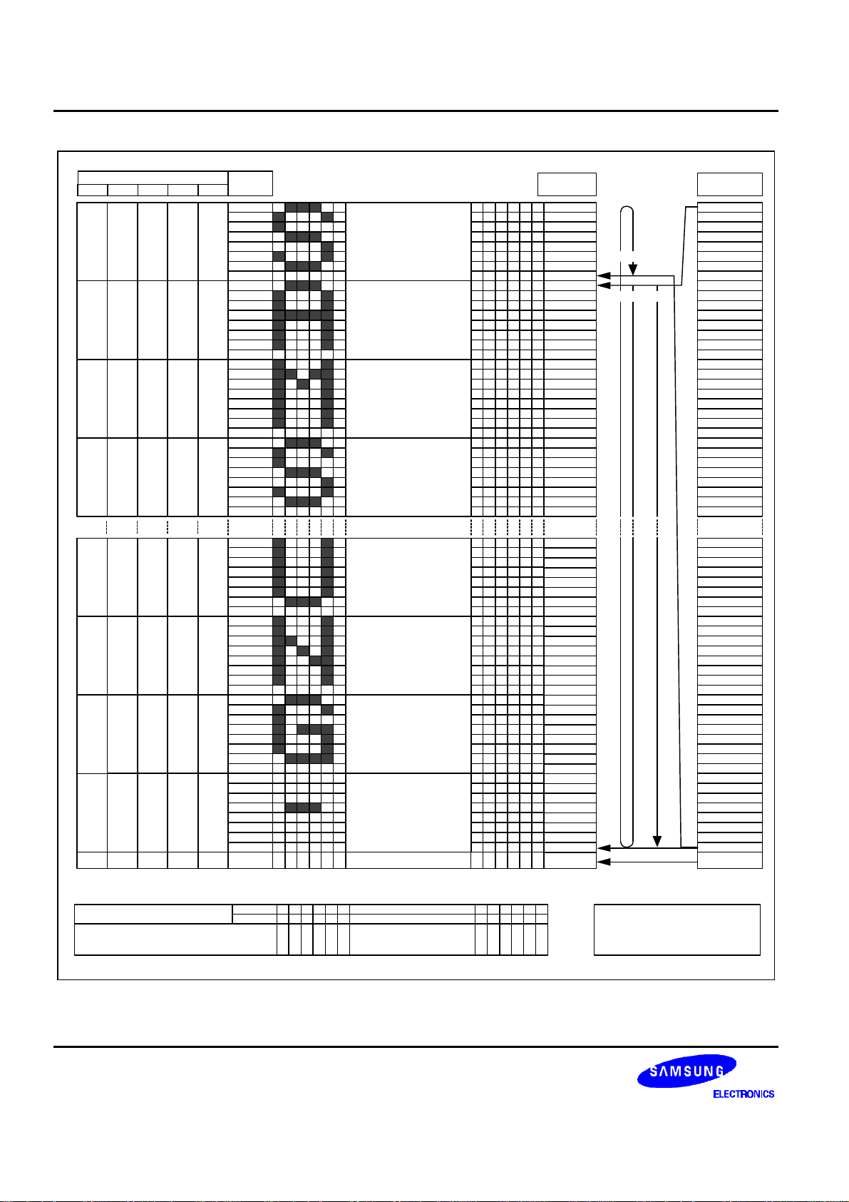
DISPLAY DATA RAM (DDRAM)
The Display Data RAM stores pixel data for the LCD. It is 129-row (17 page by 8 bits) by 128-column addressable
array. Each pixel can be selected when the page and column addresses are specified. The 129 rows are divided into
16 pages of 8 lines and the 17th page with a single line (DB0 only). Data is read from or written to the 8 lines of each
page directly through DB0 to DB7. The display data of DB0 to DB7 from the microprocessor correspond to the LCD
common lines. The microprocessor can read from and write to RAM through the I/O buffer. Since the LCD controller
operates independently, data can be written into RAM at the same time as data is being displayed without causing
the LCD flicker.
Page Address Circuit
This circuit is for providing a Page Address to Display Data RAM shown in figure 8. It incorporates 4-bit Page
Address register changed by only the “Set Page” instruction. Page Address 16 is a special RAM area for the icons
and display data DB0 is only valid.
Line Address Circuit
This circuit assigns DDRAM a Line Address corresponding to the first line (COM0) of the display. Therefore, by
setting Line Address repeatedly, it is possible to realize the screen scrolling and page switching without changing
the contents of on-chip RAM as shown in figure 8. It incorporates 7-bit Line Address register changed by only the
initial display line instruction and 7-bit counter circuit. At the beginning of each LCD frame, the contents of register
are copied to the line counter which is increased by CL signal and generates the line address for transferring the
128-bit RAM data to the display data latch circuit. When icon is enabled by setting icon control register, display data
of icons are not scrolled because the MPU can not access Line Address of icons.
18
Page 23

S6B0741 128 SEG / 129 COM DRIVER & CONTROLLER FOR STN LCD
Column Address Circuit
Column Address Circuit has a 8-bit preset counter that provides Column Address to the Display Data RAM as shown
in figure 8. When set Column Address MSB / LSB instruction is issued, 7-bit [Y7:Y1] are set and lowest bit, Y0 is set
to “0”. Since this address is increased by 1 each a read or write data instruction, microprocessor can access the
display data continuously. However, the counter is not increased and locked if a non-existing address above 7EH. It
is unlocked if a column address is set again by set Column Address MSB / LSB instruction. And the column address
counter is independent of page address register.
ADC select instruction makes it possible to invert the relationship between the Column Address and the segment
outputs. It is necessary to rewrite the display data on built-in RAM after issuing ADC select instruction. Refer to the
following figure 7.
SEG output
SEG
0
SEG
1
SEG
2
SEG
3
... ...
SEG
124
SEG
125
SEG
126
SEG
127
Column address [Y7:Y1] 00H 01H 02H 03H ... ... 7CH 7DH 7EH 7FH
Internal column
address [Y7:Y0]
00
HEX01HEX02HEX03HEX04HEX05HEX06HEX07HEX
... ...
F8
HEXF9HEXFAHEXFBHEXFCHEXFDHEXFEHEXFFHEX
Display data (ADC = 0) 1 1 1 0 0 0 0 1 ... ... 1 0 1 1 0 0 0 1
LCD panel display ... ...
Display data (ADC = 1) 0 1 0 0 1 1 1 0 ... ... 0 1 0 0 1 0 1 1
LCD panel display ... ...
Figure 7. The Relationship between the Column Address and The Segment Outputs
Segment Control Circuit
This circuit controls the display data by the display ON / OFF, reverse display ON / OFF and entire display ON / OFF
instructions without changing the data in the display data RAM.
19
Page 24
128 SEG / 129 COM DRIVER & CONTROLLER FOR STN LCD S6B0741
Page Address
DB3 DB0DB1DB2DB4
0 000
0
0 100
0
0 010
0
0 110
0
1 001
0
1 101
0
1 011
0
1 111
0
0 0001 DB0
(*) When ICON control register is set to "1", page address is set to "16". and user can write data for displaying icons.
Data
DB0
DB1
DB2
DB3
DB4
DB5
DB6
DB7
DB0
DB1
DB2
DB3
DB4
DB5
DB6
DB7
DB0
DB1
DB2
DB3
DB4
DB5
DB6
DB7
DB0
DB1
DB2
DB3
DB4
DB5
DB6
DB7
DB0
DB1
DB2
DB3
DB4
DB5
DB6
DB7
DB0
DB1
DB2
DB3
DB4
DB5
DB6
DB7
DB0
DB1
DB2
DB3
DB4
DB5
DB6
DB7
DB0
DB1
DB2
DB3
DB4
DB5
DB6
DB7
Page 0
Page 1
Page 2
Page 3
Page 12
Page 13
Page 14
Page 15
Page 16 (*)
Line
Address
00H
01H
02H
03H
04H
05H
06H
07H
08H
09H
0AH
0BH
0CH
0DH
0EH
0FH
10H
11H
12H
13H
14H
15H
16H
17H
18H
19H
1AH
1BH
1CH
1DH
1EH
1FH
60H
61H
62H
63H
64H
65H
66H
67H
68H
69H
6AH
6BH
6CH
6DH
6EH
6FH
70H
71H
72H
73H
74H
75H
76H
77H
78H
79H
7AH
7BH
7CH
7DH
7EH
7FH
End = 07H
Start = 08H
1/129 Duty
1/121 Duty
80H COMS
COM
Output
COM0
COM1
COM2
COM3
COM4
COM5
COM6
COM7
COM8
COM9
COM10
COM11
COM12
COM13
COM14
COM15
COM16
COM17
COM18
COM19
COM20
COM21
COM22
COM23
COM24
COM25
COM26
COM27
COM28
COM29
COM30
COM31
COM96
COM97
COM98
COM99
COM100
COM101
COM102
COM103
COM104
COM105
COM106
COM107
COM108
COM109
COM110
COM111
COM112
COM113
COM114
COM115
COM116
COM117
COM118
COM119
COM120
COM121
COM122
COM123
COM124
COM125
COM126
COM127
Column Address [Y7:Y1]
20
LCD Segment Output
ADC=0
ADC=1
02
0301 04 05
00
SEG0
SEG1
7C7D 7A7B7E7F
SEG2
SEG3
SEG4
SEG5
- - - - - - - -
- - - - - - - -
- - - - - - - -
Figure 8. Display Data RAM Map
SEG122
SEG123
7C 7D7A 7B 7E 7F
0203 00010405
SEG124
SEG125
SEG126
SEG127
Initial start line
address = 08H
Page 25
S6B0741 128 SEG / 129 COM DRIVER & CONTROLLER FOR STN LCD
LCD DISPLAY CIRCUITS
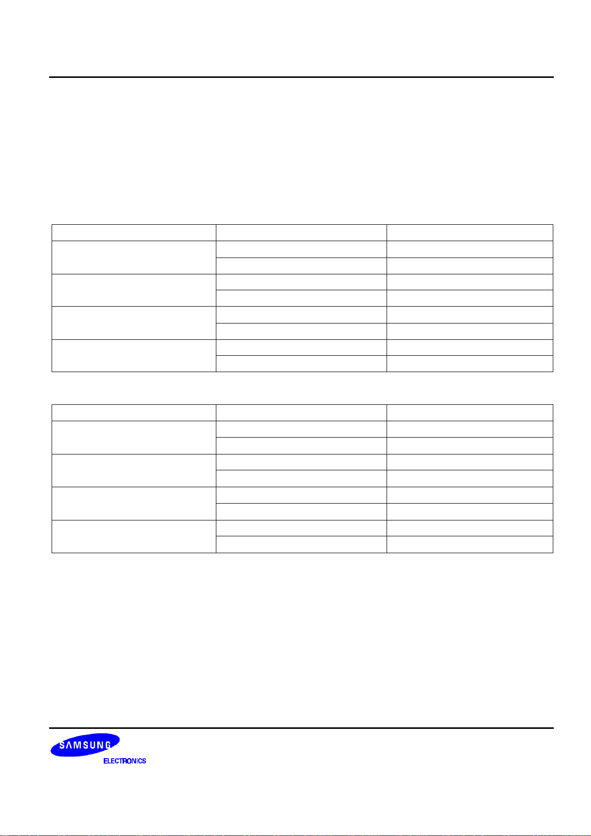
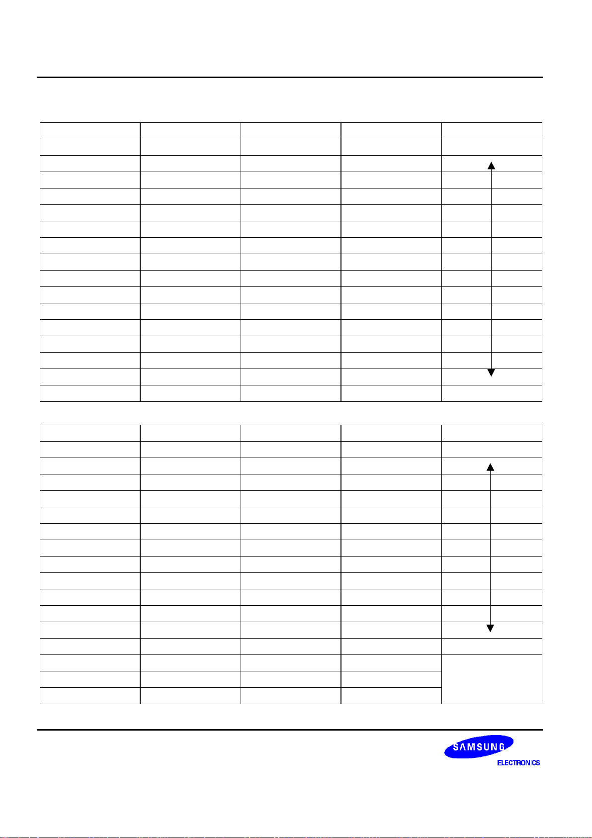
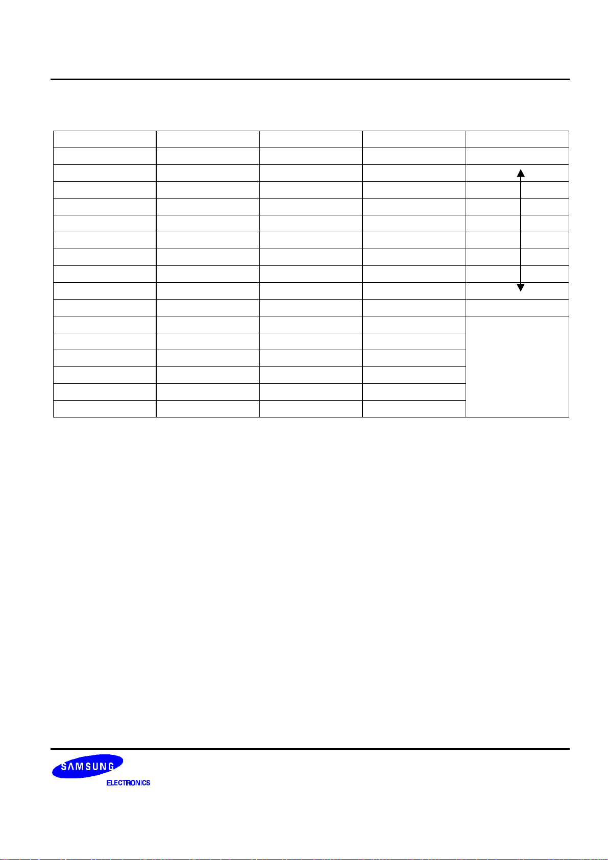
FRC (Frame Rate Control) and PWM (Pulse Width Modulation) Function Circuit
The S6B0741 incorporates an FRC function and a PWM function circuit to display a 4-level gray scale. The FRC
function and PWM utilize liquid crystal characteristics whose transmittance is changed by an effective value of
applied voltage. The S6B0741 provides four 4-bit palette-registers to assign the desired gray level. These registers
are set by the instructions and the RESETB.
− Gray Scale Table of 4 FRC (Frame Rate Control)
Gray scale level MSB (DB7 to DB4) LSB (DB3 to DB0)
White
Light gray
Dark gray
Black
2nd FR (FR2) 1st FR (FR1)
4th FR (FR4) 3rd FR (FR3)
2nd FR (FR2) 1st FR (FR1)
4th FR (FR4) 3rd FR (FR3)
2nd FR (FR2) 1st FR (FR1)
4th FR (FR4) 3rd FR (FR3)
2nd FR (FR2) 1st FR (FR1)
4th FR (FR4) 3rd FR (FR3)
− Gray Scale Table of 3 FRC (Frame Rate Control)
Gray scale level MSB (DB7 to DB4) LSB (DB3 to DB0)
2nd FR (FR2) 1st FR (FR1)
White
2nd FR (FR2) 1st FR (FR1)
Light gray
2nd FR (FR2) 1st FR (FR1)
Dark gray
2nd FR (FR2) 1st FR (FR1)
Black
× × × ×
× × × ×
× × × ×
× × × ×
3rd FR (FR3)
3rd FR (FR3)
3rd FR (FR3)
3rd FR (FR3)
21
Page 26
128 SEG / 129 COM DRIVER & CONTROLLER FOR STN LCD S6B0741
− Gray Scale Table of 15 PWM (Pulse Width Modulation)
Dec Hex 4-bits PWM (on width) Note
0 00 0000 0 (0/15) Brighter
1 01 0001 1/15
2 02 0010 2/15
3 03 0011 3/15
4 04 0100 4/15
5 05 0101 5/15
6 06 0110 6/15
7 07 0111 7/15
8 08 1000 8/15
9 09 1001 9/15
10 0A 1010 10/15
11 0B 1011 11/15
12 0C 1100 12/15
13 0D 1101 13/15
14 0E 1110 14/15
15 0F 1111 1 (15/15) Darker
− Gray Scale Table of 12 PWM (Pulse Width Modulation)
Dec Hex 4-bits PWM (on width) Note
0 00 0000 0 (0/12) Brighter
1 01 0001 1/12
2 02 0010 2/12
3 03 0011 3/12
4 04 0100 4/12
5 05 0101 5/12
6 06 0110 6/12
7 07 0111 7/12
8 08 1000 8/12
9 09 1001 9/12
10 0A 1010 10/12
11 0B 1011 11/12
12 0C 1100 1 (12/12) Darker
13 0D 1101 0/12
14 0E 1110 0/12
15 0F 1111 0/12
This area is selected to
OFF level (0/12 level)
22
Page 27
S6B0741 128 SEG / 129 COM DRIVER & CONTROLLER FOR STN LCD
− Gray Scale Table of 9 PWM (Pulse Width Modulation)
Dec Hex 4-bits PWM (on width) Note
0 00 0000 0 (0/9) Brighter
1 01 0001 1/9
2 02 0010 2/9
3 03 0011 3/9
4 04 0100 4/9
5 05 0101 5/9
6 06 0110 6/9
7 07 0111 7/9
8 08 1000 8/9
9 09 1001 1 (9/9) Darker
10 0A 1010 0/9
11 0B 1011 0/9
12 0C 1100 0/9
13 0D 1101 0/9
This area is selected to
OFF level (0/9 level)
14 0E 1110 0/9
15 0F 1111 0/9
23
Page 28
128 SEG / 129 COM DRIVER & CONTROLLER FOR STN LCD S6B0741
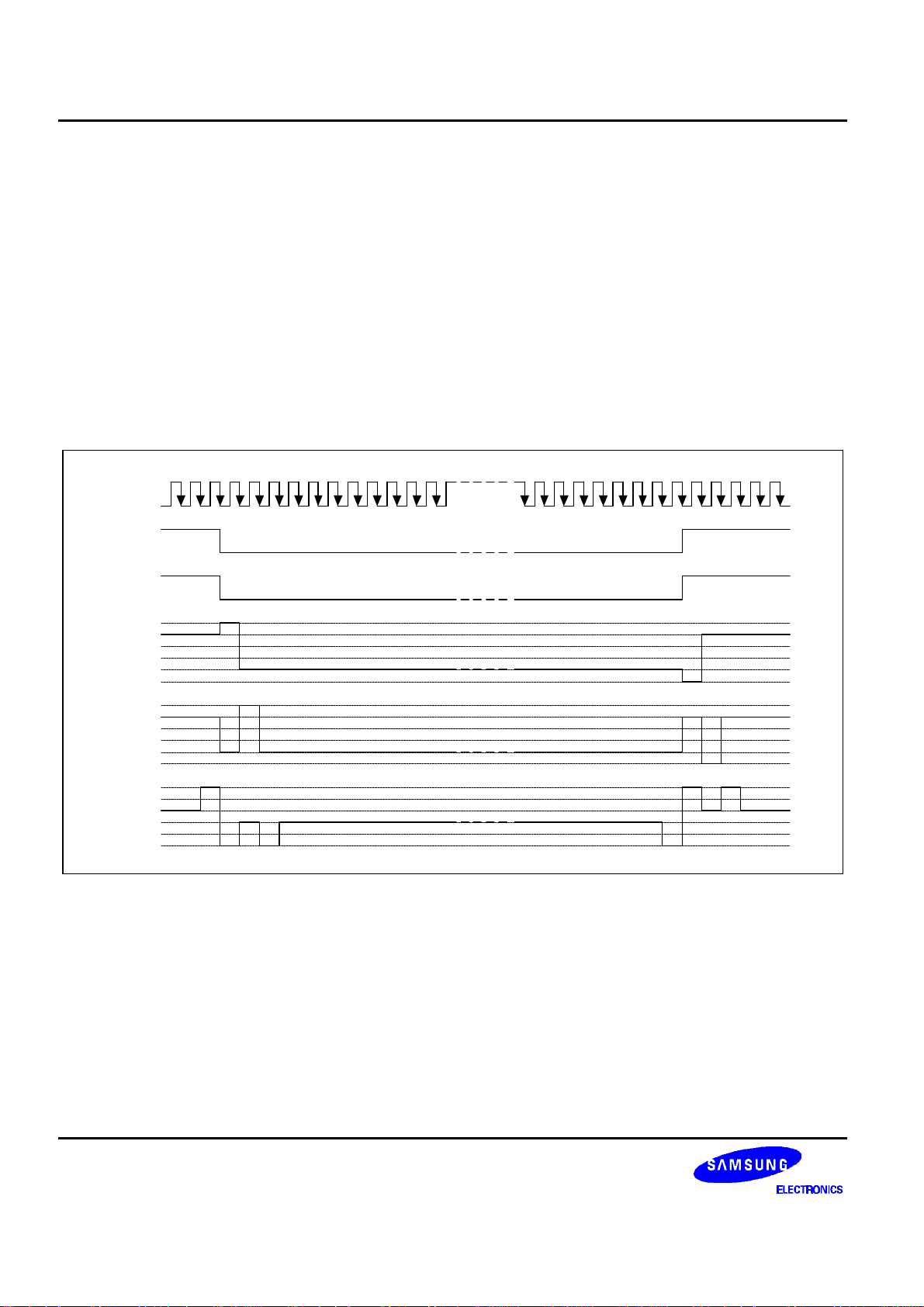
Oscillator
This is on-chip Oscillator with external resistor. Its frequency is controlled by external resistor between OSC1 and
VDD. This oscillator signal is used in the voltage converter and display timing generation circuit.
Display Timing Generator Circuit
This circuit generates some signals to be used for displaying LCD. The display clock, CL(internal), generated by
oscillation clock, generates the clock for the line counter and the signal for the display data latch. The line address of
on-chip RAM is generated in synchronization with the display clock and the display data latch circuit latches the
128-bit display data in synchronization with the display clock. The display data, which is read to the LCD driver, is
completely independent of the access to the display data RAM from the microprocessor. The display clock
generates an LCD AC signal (M) which enables the LCD driver to make a AC drive waveform, and also generates an
internal common timing signal and start signal to the common driver. The frame signal or the line signal changes the
M by setting internal instruction. Driving waveform and internal timing signal are shown in Figure 9.
127 128 1 2 3 4 5 6 7 8 9 10 11 12 121 122 123 124 125 126 127 128 1 2 3 4 5 6
CL(Internal)
FR(Internal)
M(Internal)
COM0
COM1
SEGn
Figure 9. 2-frame AC Driving Waveform (Duty Ratio = 1/128)
V0
V1
V2
V3
V4
VSS
V0
V1
V2
V3
V4
VSS
V0
V1
V2
V3
V4
VSS
24
Page 29
S6B0741 128 SEG / 129 COM DRIVER & CONTROLLER FOR STN LCD
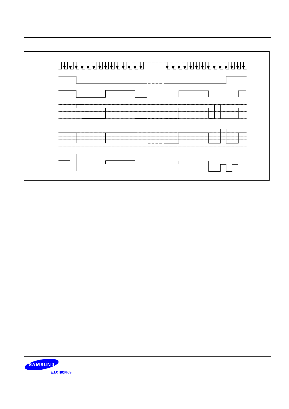
127 128 1 2 3 4 5 6 7 8 9 10 11 12 119 120 121 122 123 124 125 126 127 128 1 2 3 4
CL(Internal)
FR(Internal)
M(Internal)
V0
V1
COM0
COM1
SEGn
V2
V3
V4
VSS
V0
V1
V2
V3
V4
VSS
V0
V1
V2
V3
V4
VSS
Figure 10. N-Line Inversion Driving Waveform (N = 5, Duty Ratio = 1/128)
25
Page 30
128 SEG / 129 COM DRIVER & CONTROLLER FOR STN LCD S6B0741
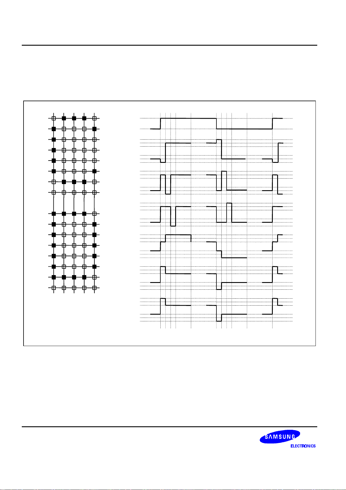
LCD DRIVER CIRCUIT
This driver circuit is configured by 129-channel common drivers and 128-channel segment drivers. This LCD panel
driver voltage depends on the combination of display data and M signal.
DD
COM0
COM1
COM2
COM3
COM4
COM5
COM6
COM7
COM8
COM9
COM10
COM11
COM12
COM13
COM14
COM15
M
COM0
COM1
COM2
SEG0
SEG1
S
S
S
S
S
E
E
E
G
0
G
G
2
1
E
E
G
G
4
3
SEG2
V
SS
V
V0
V1
V2
V3
V4
SS
V
V0
V1
V2
V3
V4
SS
V
V0
V1
V2
V3
V4
SS
V
V0
V1
V2
V3
V4
SS
V
V0
V1
V2
V3
V4
SS
V
V0
V1
V2
V3
V4
SS
V
26
Figure 11. Segment and Common Timing
Page 31
S6B0741 128 SEG / 129 COM DRIVER & CONTROLLER FOR STN LCD
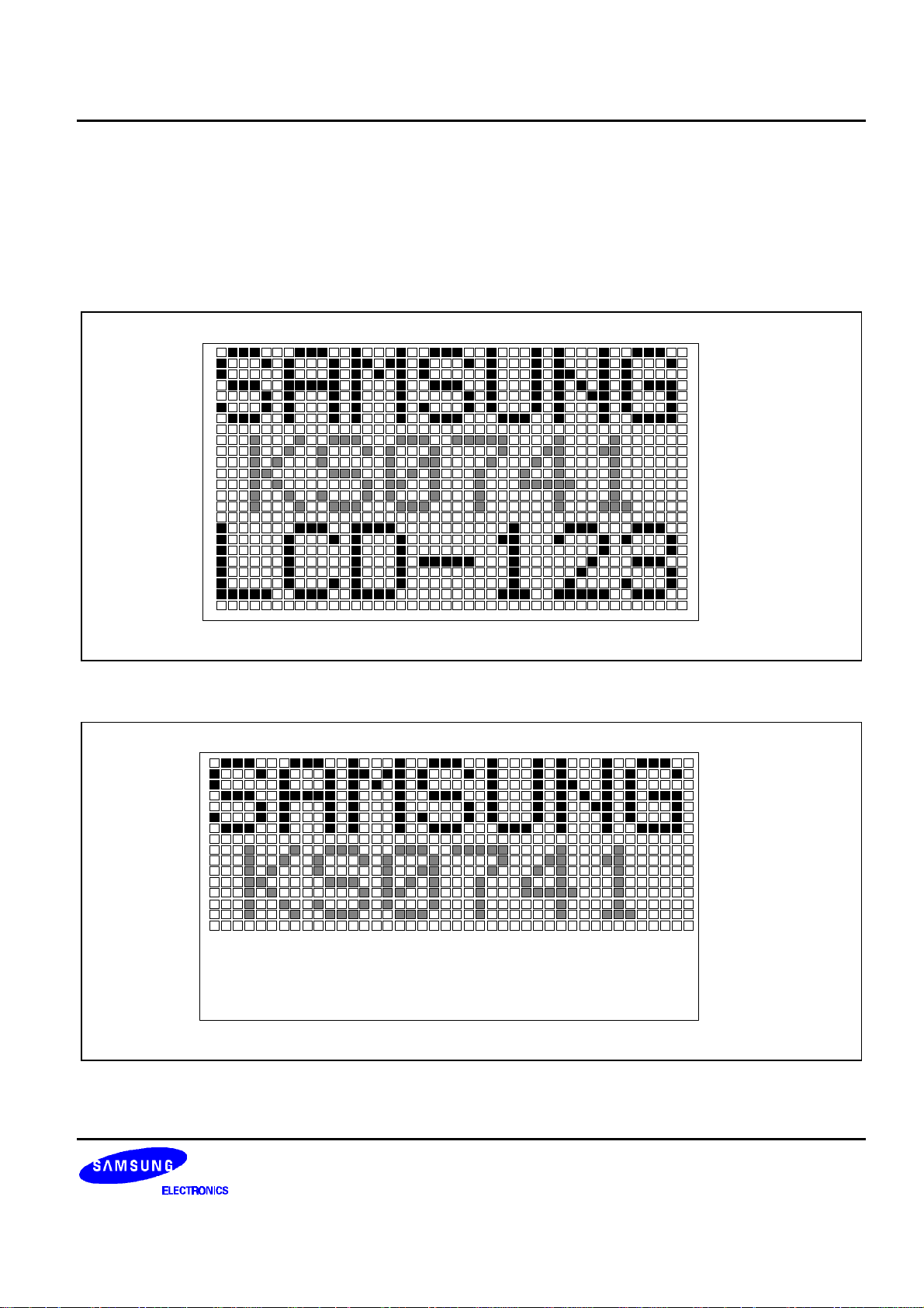
Partial Display on LCD
The S6B0741 realizes the Partial Display function on LCD with low-duty driving for saving power consumption and
showing the various display duty. To show the various display duty on LCD, LCD driving duty and bias are
programmable via the instruction. And, built-in power supply circuits are controlled by the instruction for adjusting
the LCD driving voltages
-- COM0
-- COM1
-- COM2
-- COM3
-- COM4
-- COM5
-- COM6
-- COM7
-- COM8
-- COM9
-- COM10
-- COM11
-- COM12
-- COM13
-- COM14
-- COM15
-- COM16
-- COM17
-- COM18
-- COM19
-- COM20
-- COM21
-- COM22
-- COM23
Figure 12. Reference Example for Partial Display
-- COM0
-- COM1
-- COM2
-- COM3
-- COM4
-- COM5
-- COM6
-- COM7
-- COM8
-- COM9
-- COM10
-- COM11
-- COM12
-- COM13
-- COM14
-- COM15
-- COM16
-- COM17
-- COM18
-- COM19
-- COM20
-- COM21
-- COM22
-- COM23
Figure 13. Partial Display (Partial Display Duty = 16, Initial COM0 = 0)
27
Page 32
128 SEG / 129 COM DRIVER & CONTROLLER FOR STN LCD S6B0741
-- COM0
-- COM1
-- COM2
-- COM3
-- COM4
-- COM5
-- COM6
-- COM7
-- COM8
-- COM9
-- COM10
-- COM11
-- COM12
-- COM13
-- COM14
-- COM15
-- COM16
-- COM17
-- COM18
-- COM19
-- COM20
-- COM21
-- COM22
-- COM23
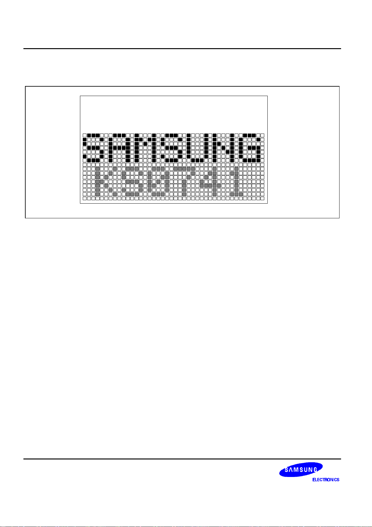
Figure 14. Moving Display (Partial Display Duty = 16, Initial COM0 = 8)
28
Page 33
S6B0741 128 SEG / 129 COM DRIVER & CONTROLLER FOR STN LCD
POWER SUPPLY CIRCUITS
The Power Supply circuits generate the voltage levels necessary to drive liquid crystal driver circuits with low power
consumption and the fewest components. There are voltage converter circuits, voltage regulator circuits, and
voltage follower circuits. They are controlled by power control instruction. For details, refers to "Instruction
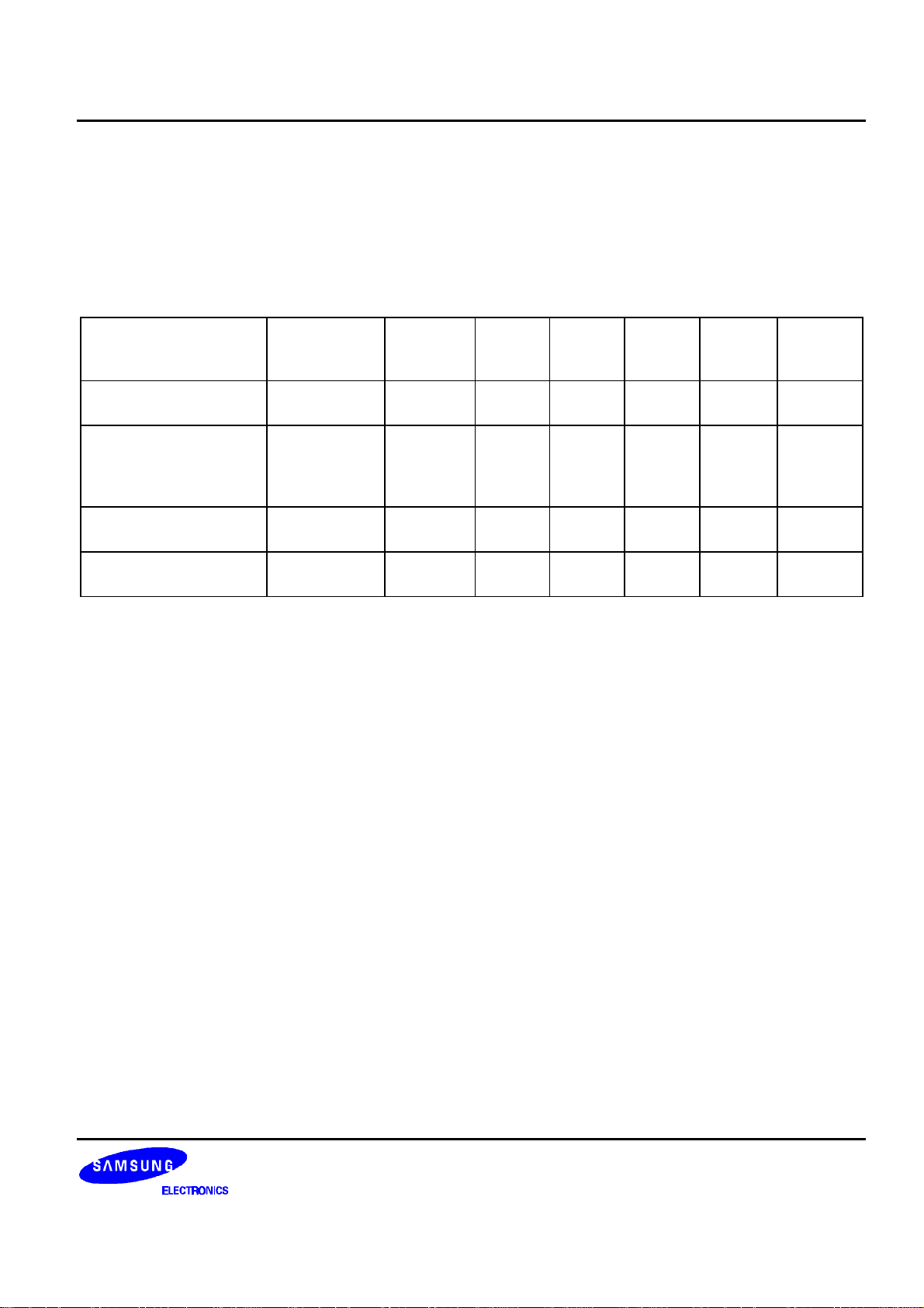
Description". Table 12 shows the referenced combinations in using Power Supply circuits.
Table 12. Recommended Power Supply Combinations
User setup
Only the internal power
supply circuits are used
Only the voltage
regulator circuits and
voltage follower circuits
are used
Only the voltage follower
circuits are used
Only the external power
supply circuits are used
Power
control
(VC VR VF)
1 1 1 ON ON ON Open Open Open
0 1 1 OFF ON ON
0 0 1 OFF OFF ON Open
0 0 0 OFF OFF OFF Open
V/C
circuits
V/R
circuits
V/F
circuits
VOUT V0 V1 to V4
External
input
Open Open
External
input
External
input
Open
External
input
29
Page 34
128 SEG / 129 COM DRIVER & CONTROLLER FOR STN LCD S6B0741
Voltage Converter Circuits
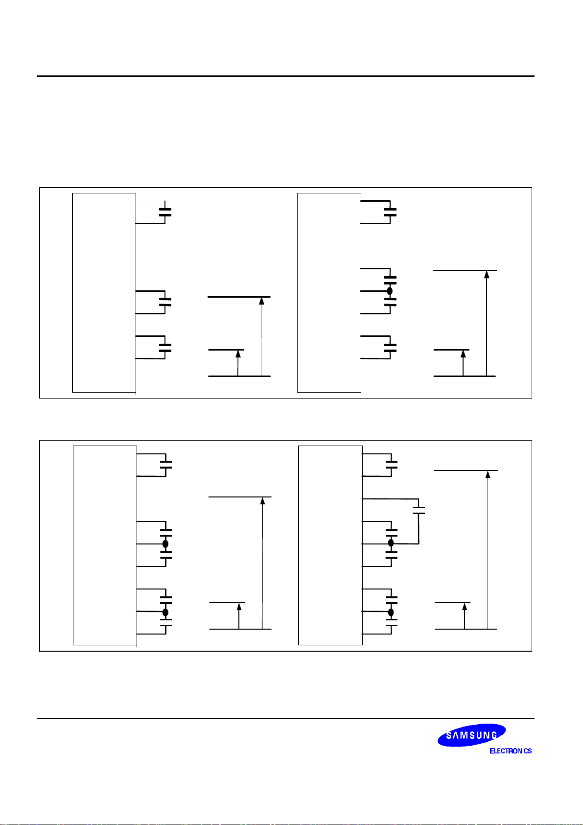
These circuits boost up the electric potential between VCI and Vss to 3, 4, 5 or 6 times toward positive side and
boosted voltage is outputted from VOUT pin. It is possible to select the lower boosting level in any boosting circuit by
“Set DC-DC Step-up” instruction. When the higher level is selected by instruction, VOUT voltage is not valid.
[C1 = 1.0 to 4.7 µF]
Vss
VOUT
C5+
C3+
C1-
C1+
C2+
C2 -
C4+
-
C1
+
-
+
+
-
-
VOUT = 3 x VCI
C1
C1
VCI
Vss
Vss
VOUT
C5+
C3+
C1-
C1+
C2+
C2 -
C4+
-
C1
+
VOUT = 4 x VCI
+
C1
-
-
-
C1
+
+
C1
-
-
VCI
Vss
Figure 15. Three Times Boosting Circuit Figure 16. Four Times Boosting Circuit
Vss
VOUT
C5+
C3+
C1-
C1+
-
C1
+
VOUT = 5 x VCI
+
C1
-
-
-
C1
+
Vss
VOUT
C5+
C3+
C1-
C1+
-
+
C1
+
-
-
-
+
VOUT = 6 x VCI
C1
+
-
-
C1
C1
30
C2+
C2 -
C4+
+
C1
-
-
-
C1
+
VCI
Vss
C2+
C2 -
C4+
+
C1
-
-
-
C1
+
VCI
Vss
Figure 17. Five Times Boosting Circuit Figure 18. Six Times Boosting Circuit
Page 35
S6B0741 128 SEG / 129 COM DRIVER & CONTROLLER FOR STN LCD
GND
RaRbVSS
VRV0VOUT
Voltage Regulator Circuits
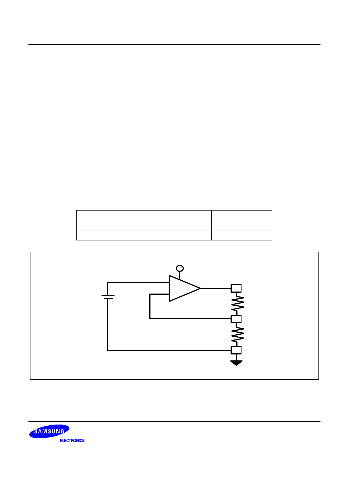
The function of the internal Voltage Regulator circuits is to determine liquid crystal operating voltage, V0, by
adjusting resistors, Ra and Rb, within the range of |V0| < |VOUT|. Because VOUT is the operating voltage of
operational-amplifier circuits shown in figure 19, it is necessary to be applied internally or externally.
For the Eq. 1, we determine V0 by Ra, Rb and VEV. The Ra and Rb are connected internally or externally by INTRS
pin. And VEV called the voltage of electronic volume is determined by Eq. 2, where the parameter α is the value
selected by instruction, "Set Reference Voltage Register", within the range 0 to 63. VREF voltage at Ta= 25°C is
shown in Table 13.
Rb
V0 = (1 + ) x VEV [V] ------ (Eq. 1)
Ra
(63 - α)
VEV = (1 - ) x VREF [V] ------ (Eq. 2)
210
Table 13 . VREF Voltage at Ta = 25°C
REF Temp. coefficient VREF [ V ]
1
-0.125% / °C
0 External input VEXT
+
V
EV
-
2.1
Figure 19. Internal Voltage Regulator Circuit
31
Page 36
128 SEG / 129 COM DRIVER & CONTROLLER FOR STN LCD S6B0741
In Case of Using Internal Resistors, Ra and Rb (INTRS = "H”)
When INTRS pin is "H", resistor Ra is connected internally between VR pin and VSS, and Rb is connected between
V0 and VR. We determine V0 by two instructions, "Regulator Resistor Select" and "Set Reference Voltage".
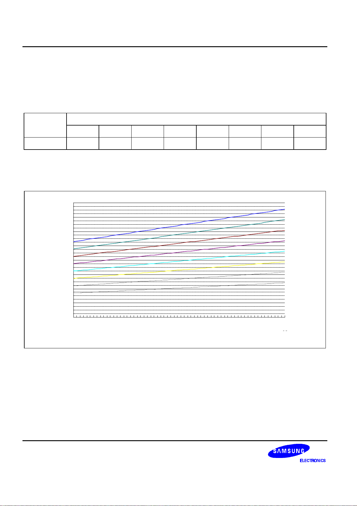
Table 14. Internal Rb / Ra Ratio depending on 3-bit Data (R2 R1 R0)
3-bit data settings (R2 R1 R0)
0 0 0 0 0 1 0 1 0 0 1 1 1 0 0 1 0 1 1 1 0 1 1 1
1 + (Rb / Ra) 2.3 3.0 3.7 4.4 5.1 5.8 6.5 7.2
Figure 20 Shows V0 voltage measured by adjusting internal regulator register ratio (Rb / Ra) and 6-bit electronic
volume registers for each temperature coefficient at Ta = 25 °C.
16.00
(1, 1, 1)
14.00
(1, 1, 0)
12.00
10.00
8.00
6.00
4.00
2.00
0.00
0 8 16 24 32 40 48 56
Electronic volume register (0 to 63)
Figure 20. Electronic Volume Level (Temp. Coefficient = -0.125% / °C)
(1, 0, 1)
(1, 0 ,0)
(0, 1, 1)
(0, 1, 0)
(0, 0, 1)
(0, 0, 0)
63
32
Page 37
S6B0741 128 SEG / 129 COM DRIVER & CONTROLLER FOR STN LCD
In Case of Using External Resistors, Ra and Rb (INTRS = "L")
When INTRS pin is "L", it is necessary to connect external regulator resistor Ra between VR and VSS, and Rb
between V0 and VR.
Example: For the following requirements
1. LCD driver voltage, V0 = 10V
2. 6-bit reference voltage register = (1, 0, 0, 0, 0, 0)
3. Maximum current flowing Ra, Rb = 1 uA
From Eq. 1
Rb
10 = (1 + ) x VEV [V] ------ (Eq. 3)
Ra
From Eq. 1
(63 - 32)
VEV = (1 - ) x 2.1 = 1.79 [V] ------ (Eq. 4)
210
From requirement 3.
10
= 1 [uA] ------ (Eq. 5)
Ra + Rb
From equations Eq. 3, 4 and 5
Ra = 1.79 [MΩ]
Rb = 8.21 [MΩ]
Table 15 Shows the Range of V0 depending on the above Requirements.
Table 15. The Range of V0
Electronic volume level
0 ....... 32 ....... 63
V0 8.21 ....... 10.00 ....... 11.73
Voltage Follower Circuits
VLCD voltage (V0) is resistively divided into four voltage levels (V1, V2, V3 and V4), and those output impedance
are converted by the Voltage Follower for increasing drive capability. Table 16 shows the relationship between V1 to
V4 level and each duty ratio.
Table 16. The Relationship between V1 to V4 Level and Each Duty Ratio
LCD bias V1 V2 V3 V4 Remarks
1/N (N-1)/N x V0 (N-2)/N x V0 2/N x V0 1/N x V0 N = 5 to 12
33
Page 38
128 SEG / 129 COM DRIVER & CONTROLLER FOR STN LCD S6B0741
VOUT
V4
VOUT
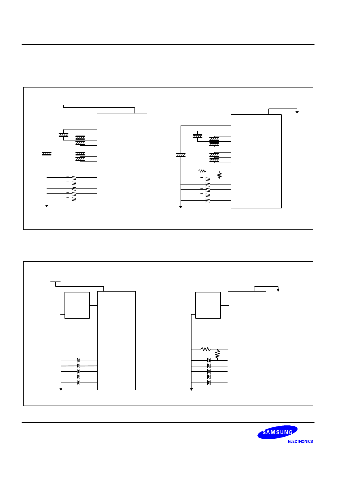
REFERENCE CIRCUIT EXAMPLES
[C1 = 1.0 to 4.7 [µF], C2 = 0.47 to 2.0 [µF]]
When using internal regulator resistors
V DD
C1
C1
C1
C2
C2
C2
C2
C2
C1
C1
+
+
+
+
+
C1
V SS
Figure 21. When Using all LCD Power Circuits (6-Time V/C: ON, V/R: ON, V/F: ON)
INTRS
VOUT
C5+
C3+
C1 C1+
C2+
C2 C4+
VR
V0
V1
V2
V3
V4
C1
V SS
When not using internal regulator resistors
INTRS
VOUT
C5+
C1
C2
C2
C2
C2
C2
C1
C1
C1
C1
Ra
+
+
+
+
+
C3+
C1 C1+
C2+
C2 C4+
VR
R
b
V0
V1
V2
V3
V4
V SS
[C2 = 0.47 to 2.0 [µF]]
When using internal regulator resistors When not using internal regulator resistors
DD
V
SS
V
V
External
Power
Supply
C2 - +
C2 - +
C2 - +
C2 - +
C2 - +
SS
INTRS
C5+
C3+
C1C1+
C2+
C2C4+
VR
V0
V1
V2
V3
V
External
Power
Supply
C2 - +
C2 - +
C2 - +
C2 - +
C2 - +
SS
Ra
INTRS
C5+
C3+
C1C1+
C2+
C2C4+
VR
Rb
V0
V1
V2
V3
V4
Figure 22. When Using some LCD Power Circuits (V/C: OFF, V/R: ON, V/F: ON)
34
Page 39
S6B0741 128 SEG / 129 COM DRIVER & CONTROLLER FOR STN LCD
VOUT
V4
VOUT
V4
[C2 = 0.47 to 2.0 [µF]]
VDD
INTRS
C5+
C3+
C1-
External
Power
Supply
C1+
C2+
C2C4+
VR
C2 - +
C2 - +
C2 - +
C2 - +
C2 - +
V0
V1
V2
V3
VSS
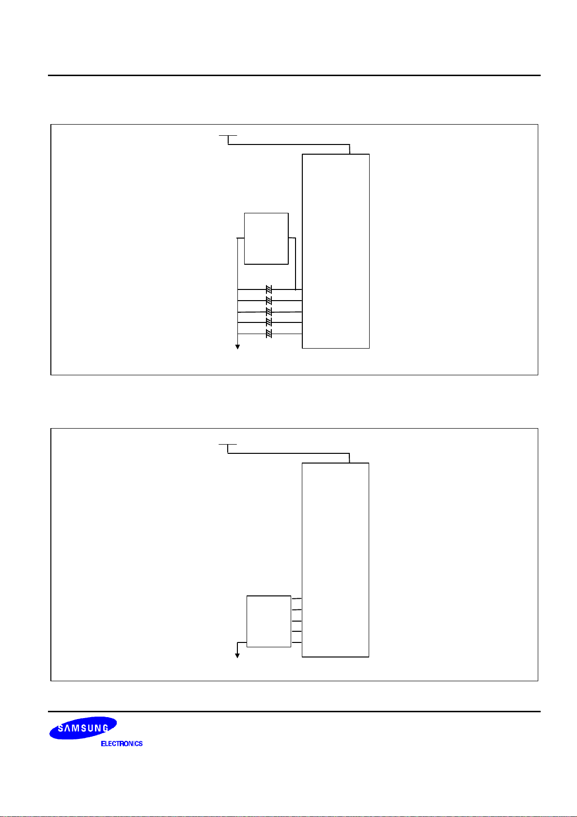
Figure 23. When Using some LCD Power Circuits (V/C: OFF, V/R: OFF, V/F: ON)
[C2 = 0.47 to 2.0 [µF]]
VDD
INTRS
C5+
C3+
C1C1+
C2+
C2C4+
VR
V0
External
Power
Supply
V1
V2
V3
VSS
Figure 24. When Not Using any Internal LCD Power Supply Circuits (V/C: OFF, V/R: OFF, V/F: OFF)
35
Page 40

128 SEG / 129 COM DRIVER & CONTROLLER FOR STN LCD S6B0741
RESET CIRCUIT
Setting RESETB to “L” or Reset instruction can initialize internal function.
When RESETB becomes “L”, following procedure is occurred.
Page address: 0
Column address: 0
Read-modify-write: OFF
Display ON / OFF: OFF
Initial display line: 0 (first)
Initial COM0 register: 0 (COM0)
Partial display duty ratio: 1/128
Reverse display ON / OFF: OFF (normal)
N-line inversion register: 0 (disable)
Entire Display ON/OFF: OFF
ICON Control register ON/OFF: OFF (ICON disable)
Power control register (VC, VR, VF) = (0, 0, 0)
DC-DC converter circuit = (0, 0)
Regulator resistor select register: (R2, R1, R0) = (0, 0, 0)
Contrast Level: 32
LCD bias ratio: 1/12
COM Scan Direction: 0
ADC Select: 0
Oscillator: OFF
Power Save Mode: Release
Display Data Length register: 0 (for SPI mode)
White mode set: OFF
White palette register (WG3, WG2, WG1, WG0) = (0, 0, 0, 0)
Light gray mode set: OFF
Light gray palette register (LG3, LG2, LG1, LG0) = (0, 0, 0, 0)
Dark gray mode set: OFF
Dark gray palette register (DG3, DG2, DG1, DG0) = (1, 1, 1, 1)
Black mode set: OFF
Black palette register (BG3, BG2, BG1, BG0) = (1, 1, 1, 1)
FRC, PWM mode: 4FRC, 9PWM
When RESET instruction is issued, following procedure is occurred.
Page address: 0
Column address: 0
Read-modify-write: OFF
Initial display line: 0 (First)
Regulator resistor select register: (R2, R1, R0) = (0, 0, 0)
Contrast Level: 32
Display Data Length register: 0 (for SPI mode)
White mode set: OFF
White palette register (WG3, WG2, WG1, WG0) = (0, 0, 0, 0)
Light gray mode set: OFF
Light gray palette register (LG3, LG2, LG1, LG0) = (0, 0, 0, 0)
Dark gray mode set: OFF
Dark gray palette register (DG3, DG2, DG1, DG0) = (1, 1, 1, 1)
Black mode set: OFF
Black palette register (BG3, BG2, BG1, BG0) = (1, 1, 1, 1)
FRC, PWM mode: 4FRC, 9PWM
While RESETB is “L” or reset instruction is executed, no instruction except read status can be accepted. Reset
status appears at DB4. After DB4 becomes ”L”, any instruction can be accepted. RESETB must be connected to the
reset pin of the MPU, and initialize the MPU and this LSI at the same time. The initialization by RESETB is essential
before used.
36
Page 41
S6B0741 128 SEG / 129 COM DRIVER & CONTROLLER FOR STN LCD
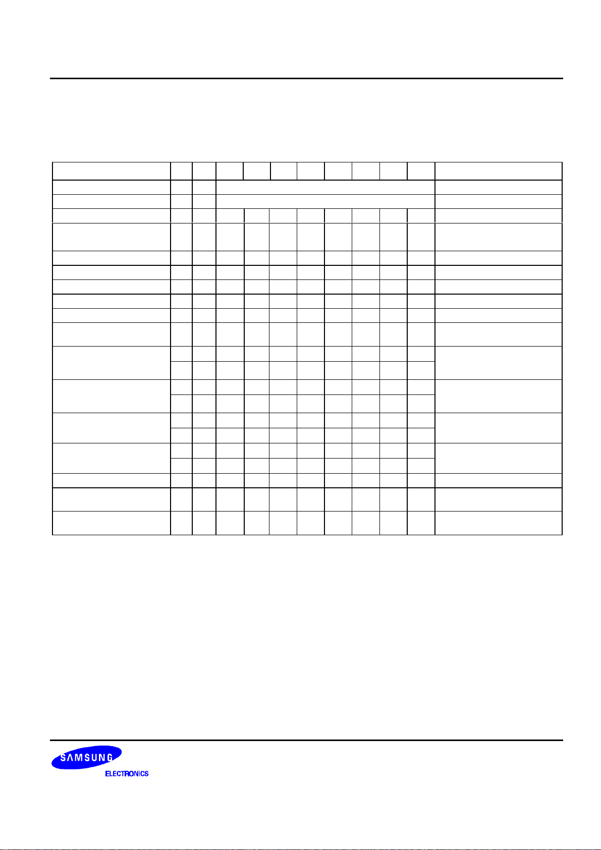
INSTRUCTION DESCRIPTION
Table 17. Instruction Table
×´ : Don’ t care
Instruction
Read display data 1 1 Read data Read data from DDRAM
Write display data 1 0 Write data Write data into DDRAM
Read status 0 1
ICON control register ON/OFF 0 0 1 0 1 0 0 0 1
Set page address 0 0 1 0 1 1 P3 P2 P1 P0 Set page address
Set column address MSB 0 0 0 0 0 1 0 Y7 Y6 Y5 Set column address MSB
Set column address LSB 0 0 0 0 0 0 Y4 Y3 Y2 Y1 Set column address LSB
Set modify-read 0 0 1 1 1 0 0 0 0 0 Set modify-read mode
Reset modify-read 0 0 1 1 1 0 1 1 1 0 release modify-read mode
Display ON/OFF 0 0 1 0 1 0 1 1 1 D
Set initial display line register
Set initial COM0 register
Set partial display duty ratio
Set N-line inversion
Release N-line inversion 0 0 1 1 1 0 0 1 0 0 Release N-line Inversion mode
Reverse display ON/OFF 0 0 1 0 1 0 0 1 1 REV
Entire display ON/OFF 0 0 1 0 1 0 0 1 0 EON
RS RW DB7 DB6 DB5 DB4 DB3 DB2 DB1 DB0
BUSY ON RES MF2 MF1 MF0 DS1 DS0
ICON
0 0 0 1 0 0 0 0
0 0
0 0 0 1 0 0 0 1
0 0
0 0 0 1 0 0 1 0
0 0 D7 D6 D5 D4 D3 D2 D1 D0
0 0 0 1 0 0 1 1
0 0
S6 S5 S4 S3 S2 S1 S0
×´
C6 C5 C4 C3 C2 C1 C0
×´
×´ ×´ ×´
N4 N3 N2 N 1 N0
×´ ×´
×´ ×´
×´ ×´
×´ ×´
Description
Read the internal status
ICON=0: ICON disable (default)
ICON=1: ICON enable & set
the page address to 16
D=0: display OFF
D=1: display ON
2-byte instruction to specify the
initial display line to realize
vertical scrolling
2-byte instruction to specify the
initial COM0 to realize window
scrolling
2-byte instruction to set partial
display duty ratio
2-byte instruction to set N-line
inversion register
REV=0: normal display,
REV=1: reverse display
EON=0: normal display.
EON=1: entire display ON
37
Page 42
128 SEG / 129 COM DRIVER & CONTROLLER FOR STN LCD S6B0741
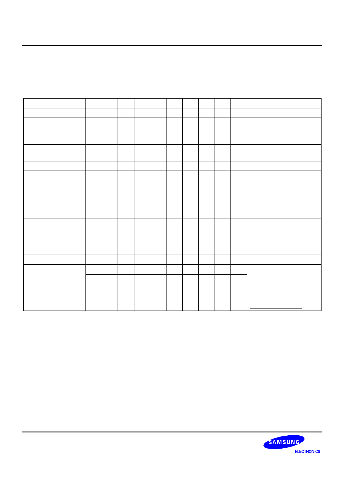
Table 17. Instruction Table (Continued)
×´ : Don’ t care
Instruction
Power control 0 0 0 0 1 0 1 VC VR VF Control power circuit operation
Select DC-DC step-up 0 0 0 1 1 0 0 1 DC1 DC0
Select regulator resistor 0 0 0 0 1 0 0 R2 R1 R0
Set electronic volume
register
Select LCD bias 0 0 0 1 0 1 0 B2 B1 B0 Select LCD bias
SHL select 0 0 1 1 0 0 SHL ×´ ×´ ×´
ADC select 0 0 1 0 1 0 0 0 0 ADC
Oscillator on start 0 0 1 0 1 0 1 0 1 1 Start the built-in oscillator
Set power save mode 0 0 1 0 1 0 1 0 0 P
Release power save mode 0 0 1 1 1 0 0 0 0 1 Release power save mode
Reset 0 0 1 1 1 0 0 0 1 0 Initialize the internal functions
Set data direction &
display data length(DDL)
NOP 0 0 1 1 1 0 0 0 1 1
Test Instruction 0 0 1 1 1 1 ×´ ×´ ×´ ×´
RS RW DB7 DB6 DB5 DB4 DB3 DB2 DB1 DB0
0 0 1 0 0 0 0 0 0 1
0 0
×´ ×´ 1 1 1 0 1 0 0 0
×´ ×´ D7 D6 D5 D4 D3 D2 D1 D0
×´ ×´
EV5 EV4 EV3 EV2 EV1 EV0
Select the step-up of the internal
voltage converter
Select internal resistance ratio of
the regulator resistor
2-byte instruction to specify the
Reference voltage
COM bi-directional selection
SHL=0: normal direction
SHL=1: reverse direction
SEG bi-directional selection
ADC=0: normal direction
ADC=1: reverse direction
P=0: normal mode
P=1: sleep mode
2-byte instruction to specify the
number of data bytes.
(SPI Mode)
No operation
Don't use this instruction.
Description
38
Page 43
S6B0741 128 SEG / 129 COM DRIVER & CONTROLLER FOR STN LCD
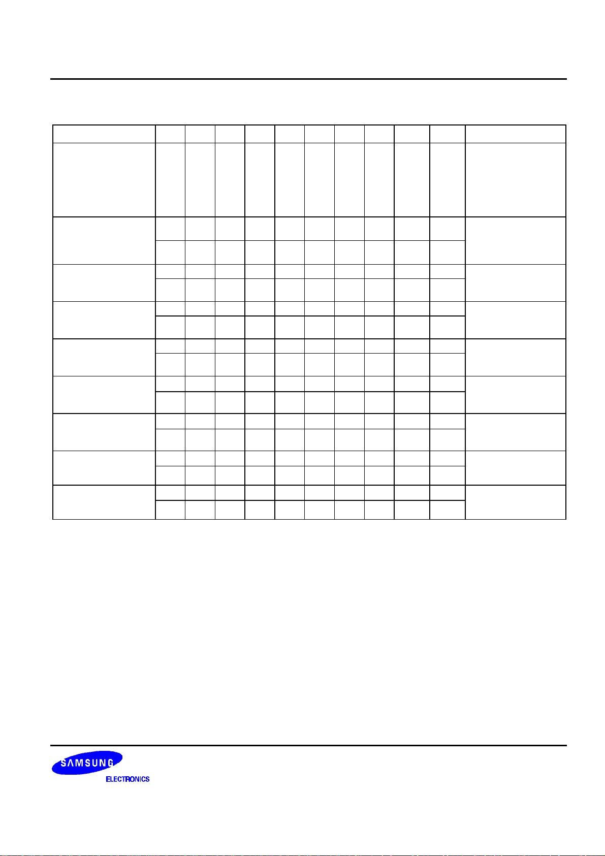
Table 17. Instruction Table (Continued)
Instruction
Set FRC and PWM mode 0 0 1 0 0 1 0 FRC PWM1 PWM0
Set white mode and
1st/2nd frame, set
pulse width
Set white mode and
3rd/4th frame, set
pulse width
Set light gray mode and
1st/2nd frame, set
pulse width
Set light gray mode and
3rd/4th frame, set
pulse width
Set dark gray mode and
1st/2nd frame, set
pulse width
Set dark gray mode and
3rd/4th frame, set
pulse width
Set black mode and
1st/2nd frame, set
pulse width
Set black mode and
3rd/4th frame, set
pulse width
RS RW DB7 DB6 DB5 DB4 DB3 DB2 DB1 DB0
0 0 1 0 0 0 1 0 0 0
0 0 WB3 WB2 WB1 WB0 WA3 WA2 WA1 WA0
0 0 1 0 0 0 1 0 0 1
0 0 WD3 WD2 WD1 WD0 WC3 WC2 WC1 WC0
0 0 1 0 0 0 1 0 1 0
0 0 LB3 LB2 LB1 LB0 LA3 LA2 LA1 LA0
0 0 1 0 0 0 1 0 1 1
0 0 LD3 LD2 LD1 LD0 LC3 LC2 LC1 LC0
0 0 1 0 0 0 1 1 0 0
0 0 DB3 DB2 DB1 DB0 DA3 DA2 DA1 DA0
0 0 1 0 0 0 1 1 0 1
0 0 DD3 DD2 DD1 DD0 DC3 DC2 DC1 DC0
0 0 1 0 0 0 1 1 1 0
0 0 BB3 BB2 BB1 BB0 BA3 BA2 BA1 BA0
0 0 1 0 0 0 1 1 1 1
0 0 BD3 BD2 BD1 BD0 BC3 BC2 BC1 BC0
Description
FRC(1:3FRC, 0:4FRC)
PWM1 PWM0
0 0 9PWM
0 1 9PWM
1 0 12PWM
1 1 15PWM
Set white mode and
1st/2nd frame
Set white mode and
3rd/4th frame
Set light gray mode and
1st/2nd frame
Set light gray mode and
3rd/4th frame
Set dark gray mode and
1st/2nd frame
Set dark gray mode and
3rd/4th frame
Set black mode and
1st/2nd frame
Set black mode and
3rd/4th frame
39
Page 44
128 SEG / 129 COM DRIVER & CONTROLLER FOR STN LCD S6B0741
Read Display Data
8-bit data from Display Data RAM specified by the column address and page address can be read by this
instruction. As the column address is increased by 1 automatically after each this instruction, the
microprocessor can continuously read data from the addressed page. A dummy read is required after loading
an address into the column address register. Display Data cannot be read through the serial interface.
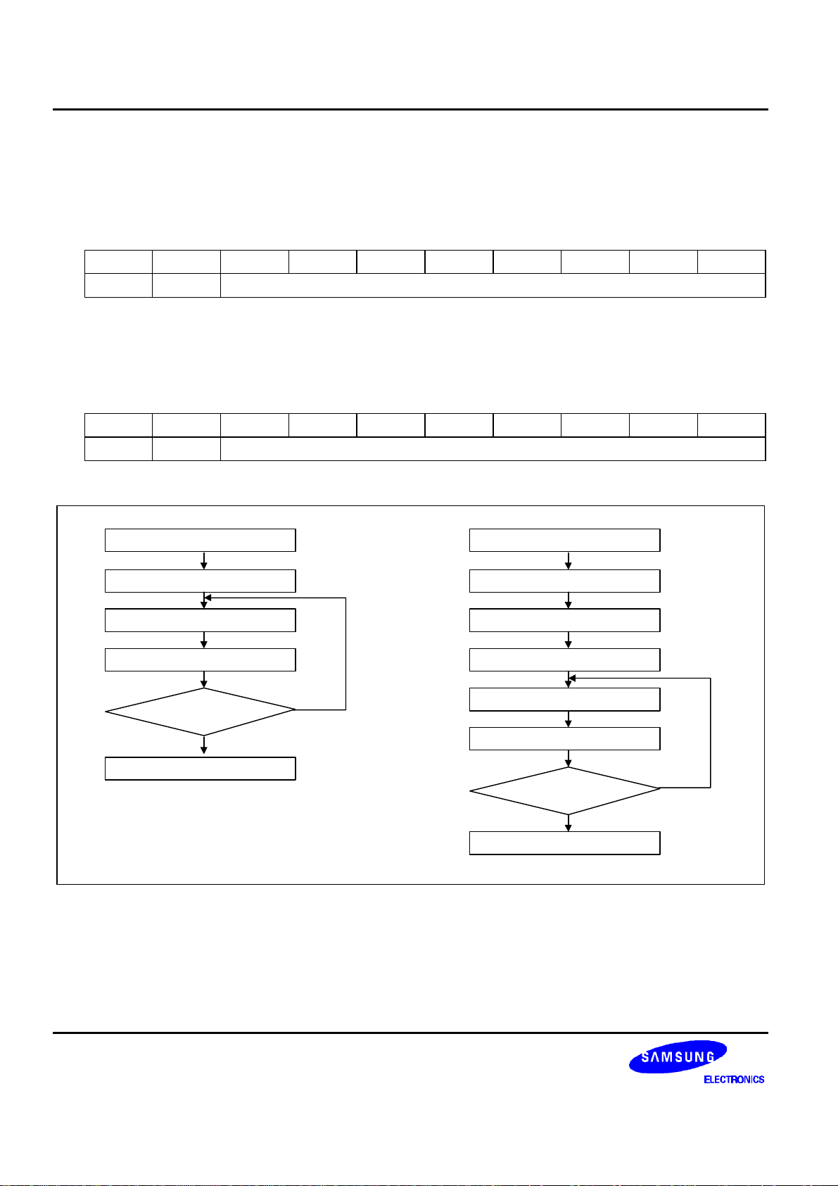
RS RW DB7 DB6 DB5 DB4 DB3 DB2 DB1 DB0
1 1 Read data
Write Display Data
8-bit data of Display Data from the microprocessor can be written to the RAM location specified by the column
address and page address. The column address is increased by 1 automatically so that the microprocessor can
continuously write data to the addressed page. During auto-increment, the column address wraps to 0 after the
last column is written
RS RW DB7 DB6 DB5 DB4 DB3 DB2 DB1 DB0
1 0 Write data
Set Page Address
Set Column Address
Data Write
Column = Column + 1
Data Write Continue ?
NO
Optional Status
YES
Set Page Address
Set Column Address
Dummy Data Read
Column = Column + 1
Data Read
Column = Column + 1
Data Read Continue ?
NO
Optional Status
YES
Figure 25. Sequence for Writing Display Data Figure 26. Sequence for Reading Display Data
40
Page 45
S6B0741 128 SEG / 129 COM DRIVER & CONTROLLER FOR STN LCD
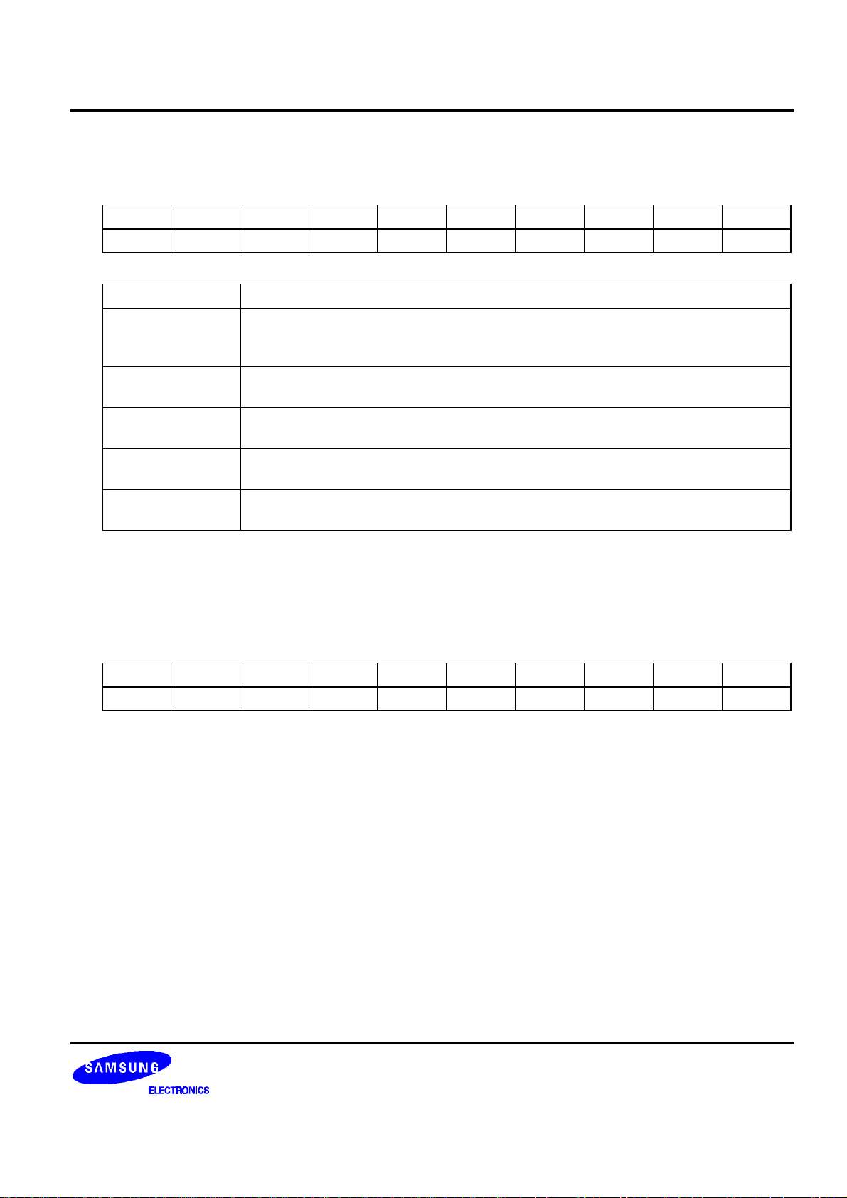
Read Status
Indicates the internal status of the S6B0741
RS RW DB7 DB6 DB5 DB4 DB3 DB2 DB1 DB0
0 1 BUSY ON / OFF RES MF2 MF1 MF0 DS1 DS0
Flag Description
The device is busy when internal operation or reset. Any instruction is rejected until
BUSY
BUSY goes Low.
0: chip is active, 1: chip is being busy
ON / OFF
RESET
Indicates display ON / OFF status
0: display OFF, 1: display ON
Indicates the initialization is in progress by RESET signal.
0: chip is active, 1: chip is being reset
MF Manufacturer ID, MF2 MF1 MF0 = [0 0 0]
DS Display size ID, DS1 DS0 = [1 0]
ICON Control Register ON/OFF
This instruction makes ICON enable or disable. By default, ICON display is disabled (ICON= 0). When ICON
control register is set to “1”, ICON display is enabled and page address is set to “16”. Then user can write data
for icons. It is impossible to set the page address to “16” by Set Page Address instruction. Therefore, when
writing data for icons, ICON control register ON instruction would be used to set the page address to “16”. When
ICON control register is set to “0”, ICON display is disabled.
RS RW DB7 DB6 DB5 DB4 DB3 DB2 DB1 DB0
0 0 1 0 1 0 0 0 1 ICON
ICON=0: ICON disable (default)
ICON=1: ICON enable & set the page address to 16
41
Page 46
128 SEG / 129 COM DRIVER & CONTROLLER FOR STN LCD S6B0741
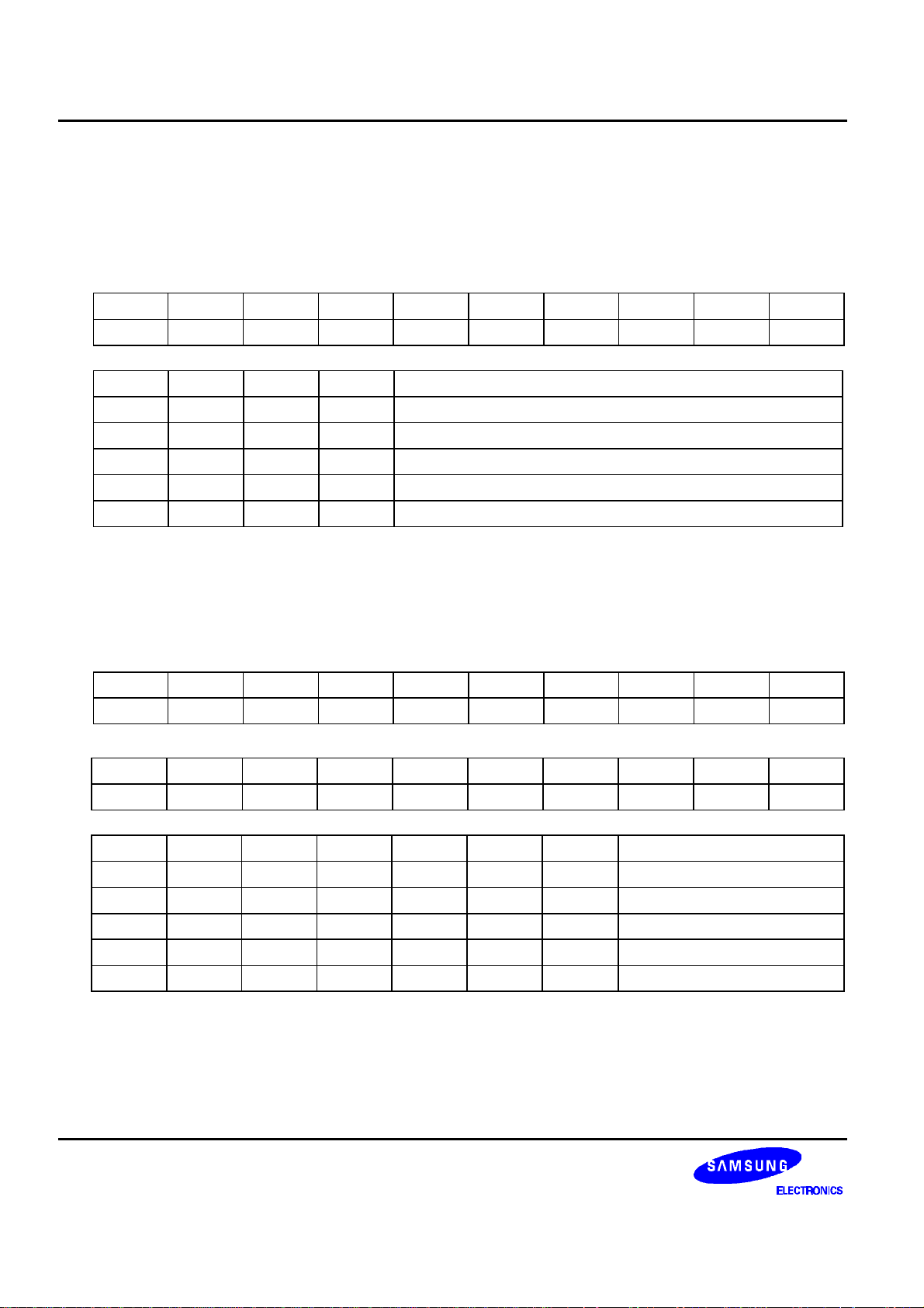
Set Page Address
Sets the Page Address of display data RAM from the microprocessor into the page address register. Any RAM
data bit can be accessed when its Page Address and column address are specified. Along with the column
address, the Page Address defines the address of the display RAM to write or read display data. Changing the
Page Address doesn't effect to the display status. Set Page Address instruction can not be used to set the page
address to “16”. Use ICON control register ON/OFF instruction to set the page address to “16”.
RS RW DB7 DB6 DB5 DB4 DB3 DB2 DB1 DB0
0 0 1 0 1 1 P3 P2 P1 P0
P3 P2 P1 P0 Page
0 0 0 0 0
0 0 0 1 1
: : : : :
1 1 1 0 14
1 1 1 1 15
Set Column Address
Sets the Column Address of display RAM from the microprocessor into the column address register. Along with
the Column Address, the Column Address defines the address of the display RAM to write or read display data.
When the microprocessor reads or writes display data to or from display RAM, Column Addresses are
automatically increased.
Set Column Address MSB
RS RW DB7 DB6 DB5 DB4 DB3 DB2 DB1 DB0
0 0 0 0 0 1 0 Y7 Y6 Y5
Set Column Address LSB
RS RW DB7 DB6 DB5 DB4 DB3 DB2 DB1 DB0
0 0 0 0 0 0 Y4 Y3 Y2 Y1
Y7 Y6 Y5 Y4 Y3 Y2 Y1 Column address [Y7:Y1]
0 0 0 0 0 0 0 0
0 0 0 0 0 0 1 1
: : : : : : : :
1 1 1 1 1 1 0 126
1 1 1 1 1 1 1 127
42
Page 47
S6B0741 128 SEG / 129 COM DRIVER & CONTROLLER FOR STN LCD
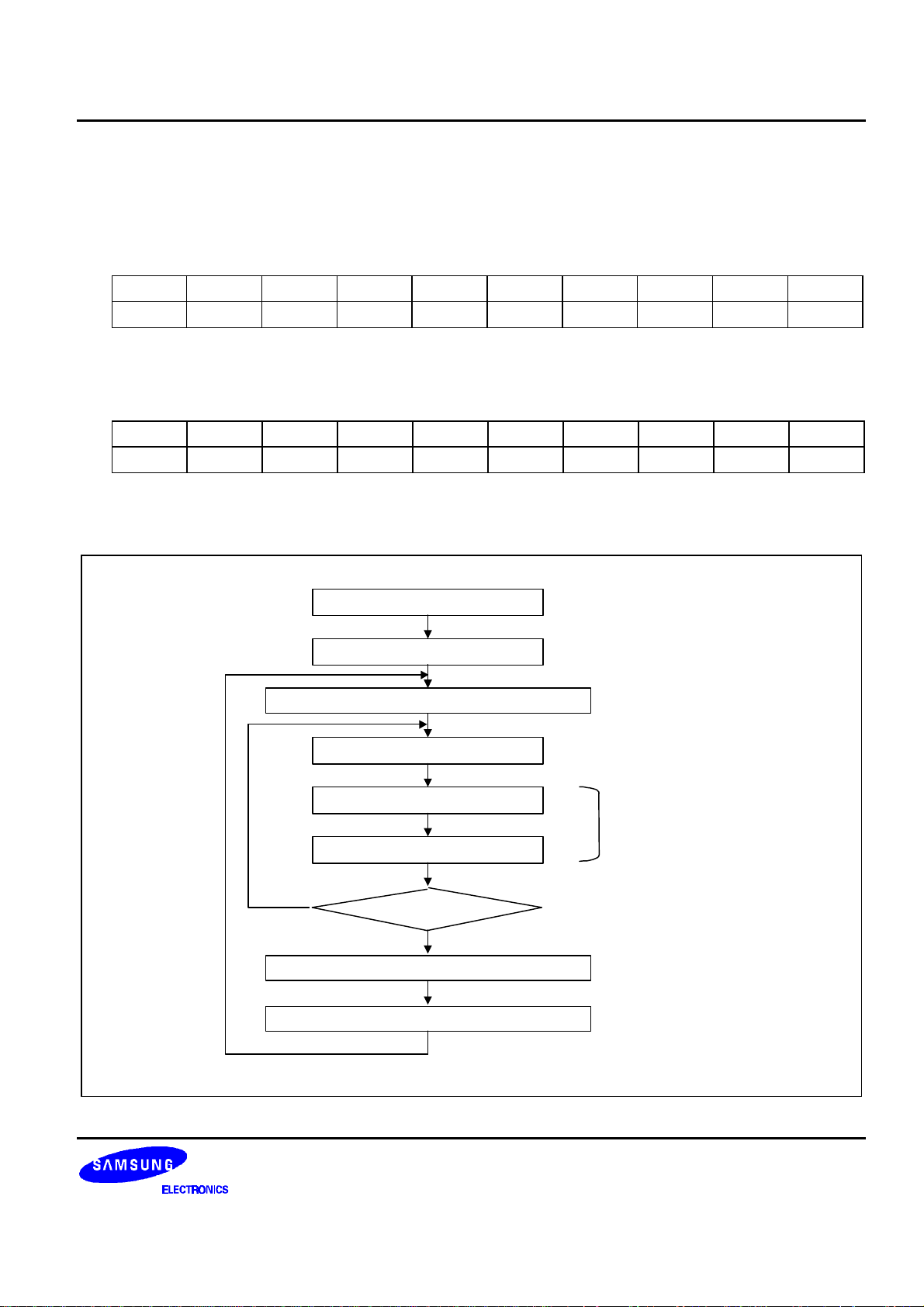
Set Modify-Read
This instruction stops the automatic increment of the column address by the read display data instruction, but
the column address is still increased by the write display data instruction. And it reduces the load of
microprocessor when the data of a specific area is repeatedly changed during cursor blinking or others. This
mode is canceled by the reset Modify-Read instruction.
RS RW DB7 DB6 DB5 DB4 DB3 DB2 DB1 DB0
0 0 1 1 1 0 0 0 0 0
Reset Modify-Read
This instruction cancels the Modify-Read mode, and makes the column address return to its initial value just
before the set Modify-Read instruction is started.
RS RW DB7 DB6 DB5 DB4 DB3 DB2 DB1 DB0
0 0 1 1 1 0 1 1 1 0
NO
Set Page Address
Set Column Address (N)
Set Modify-read
Dummy Read
Data Read
Data Process
Data Write
Change Completed?
YES
Reset Modify-read
Return Column Address (N)
Figure 27. Sequence for Cursor Display
43
Page 48
128 SEG / 129 COM DRIVER & CONTROLLER FOR STN LCD S6B0741
Setting
I
initial
D
isplay
L
ineEnd
Display ON / OFF
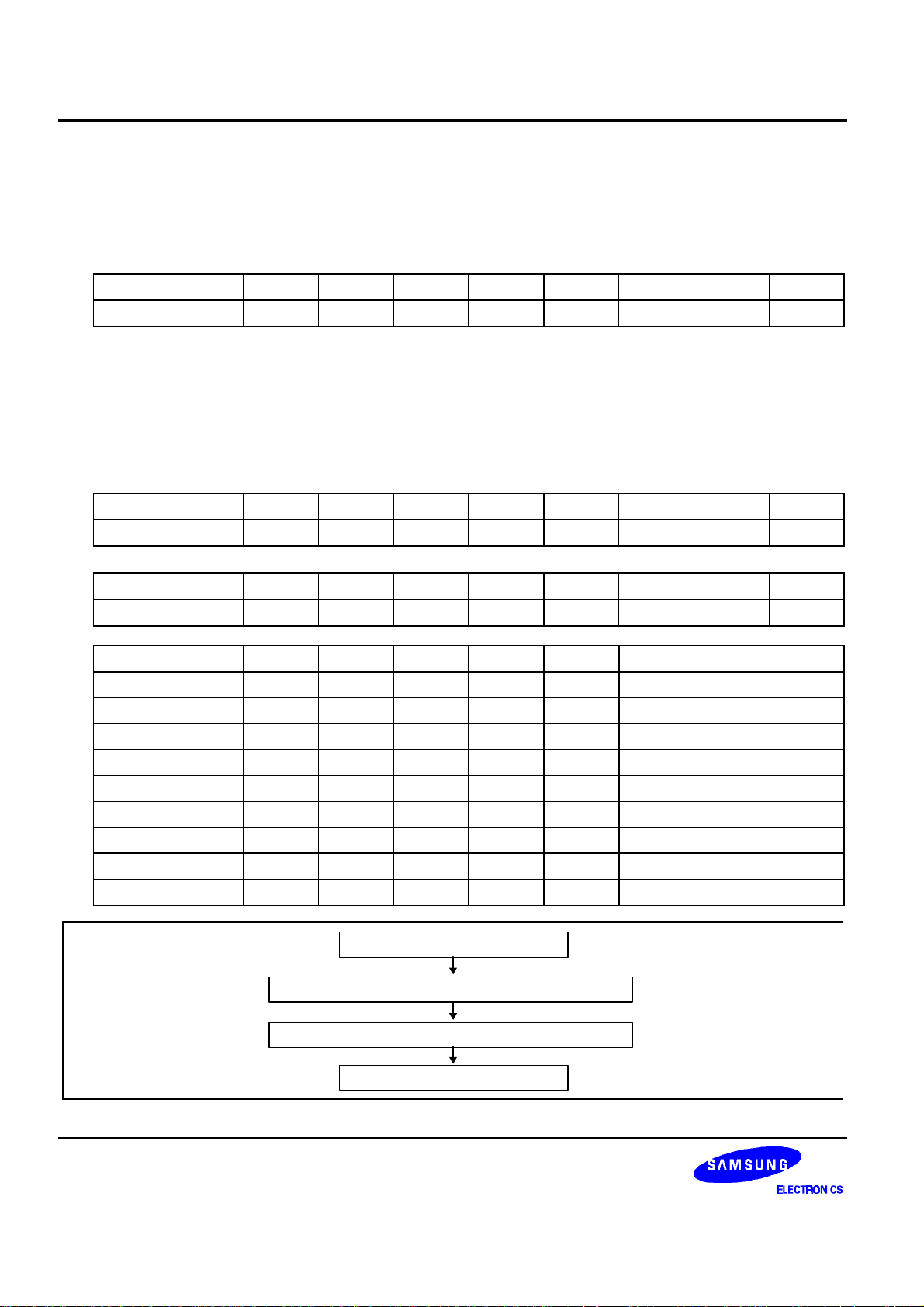
Turns the display ON or OFF.
This command has priority over Entire Display On/Off and Reverse Display On/Off. Commands are accepted
while the display is off, but the visual state of the display does not change.
RS RW DB7 DB6 DB5 DB4 DB3 DB2 DB1 DB0
0 0 1 0 1 0 1 1 1 DON
DON = 1: display ON
DON = 0: display OFF
Set Initial Display Line Register
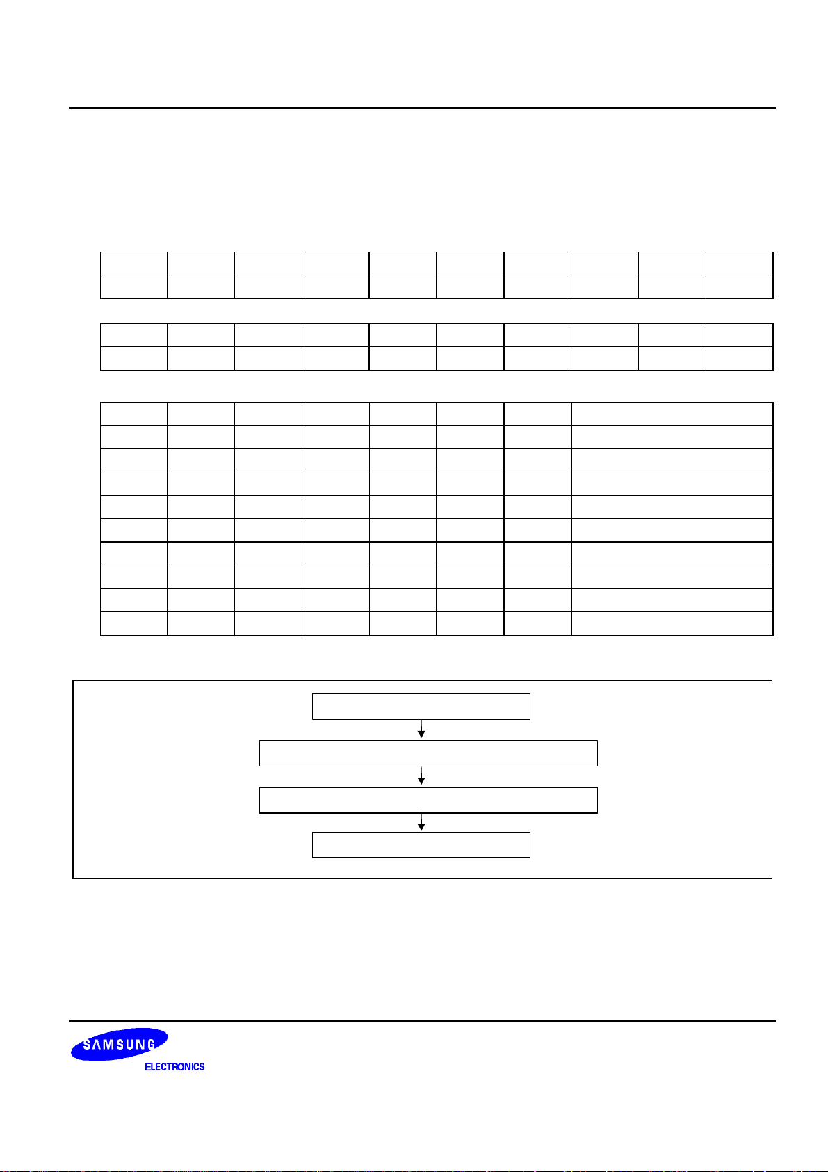
Sets the line address of display RAM to determine the initial display line using 2-byte instruction. The RAM
display data is displayed at the top of row(COM0) of LCD panel.
The 1st Instruction
RS RW DB7 DB6 DB5 DB4 DB3 DB2 DB1 DB0
0 0 0 1 0 0 0 0
× ×
The 2nd Instruction
RS RW DB7 DB6 DB5 DB4 DB3 DB2 DB1 DB0
0 0
×
S6 S5 S4 S3 S2 S1 S0
S6 S5 S4 S3 S2 S1 S0 Line address
0 0 0 0 0 0 0 0
0 0 0 0 0 0 1 1
0 0 0 0 0 1 0 2
0 0 0 0 0 1 1 3
: : : : : : : :
1 1 1 1 1 0 0 124
1 1 1 1 1 0 1 125
1 1 1 1 1 1 0 126
1 1 1 1 1 1 1 127
Setting Initial Display Line Start
44
1
Instruction (2-byte Instruction for Mode Setting)
2
Instruction (2-byte Instruction for Register S
etting)
Figure 28. The Sequence for Setting the Initial Display Line
Page 49
S6B0741 128 SEG / 129 COM DRIVER & CONTROLLER FOR STN LCD
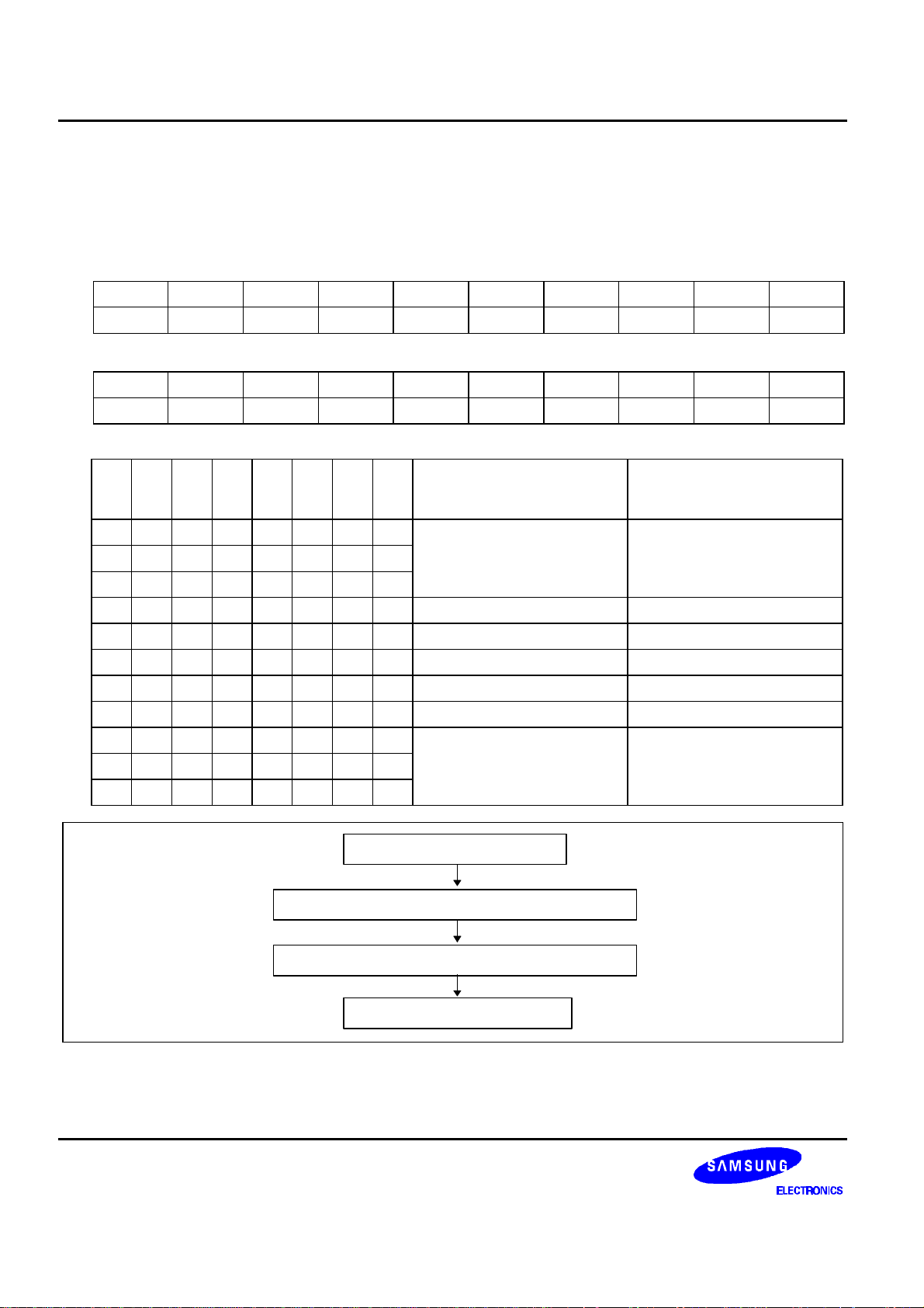
Set Initial COM0 Register
Sets the initial row (COM) of the LCD panel using the 2-byte instruction. By using this instruction, it is possible to
realize the window moving without the change of display data.
The 1st Instruction
RS RW DB7 DB6 DB5 DB4 DB3 DB2 DB1 DB0
0 0 0 1 0 0 0 1
× ×
The 2nd Instruction
RS RW DB7 DB6 DB5 DB4 DB3 DB2 DB1 DB0
0 0
×
C6 C5 C4 C3 C2 C1 C0
C6 C5 C4 C3 C2 C1 C0 Initial COM0
0 0 0 0 0 0 0 COM0
0 0 0 0 0 0 1 COM1
0 0 0 0 0 1 0 COM2
0 0 0 0 0 1 1 COM3
: : : : : : : :
1 1 1 1 1 0 0 COM124
1 1 1 1 1 0 1 COM125
1 1 1 1 1 1 0 COM126
1 1 1 1 1 1 1 COM127
Setting Initial COM0 Start
1st Instruction (Mode Setting)
2nd Instruction (Initial COM0 Setting)
Setting Initial COM0 End
Figure 29. Sequence for Setting the Initial COM0
45
Page 50
128 SEG / 129 COM DRIVER & CONTROLLER FOR STN LCD S6B0741
Set Partial Display Duty Ratio
Sets the duty ratio within range of 16 to 128 (ICON disabled) or 17 to 129 (ICON enabled) to realize partial
display by using the 2-byte instruction.
The 1st Instruction
RS RW DB7 DB6 DB5 DB4 DB3 DB2 DB1 DB0
0 0 0 1 0 0 1 0
× ×
The 2nd Instruction
RS RW DB7 DB6 DB5 DB4 DB3 DB2 DB1 DB0
0 0 D7 D6 D5 D4 D3 D2 D1 D0
D7 D6 D5 D4 D3 D2 D1 D0
Selected partial duty ratio
(ICON disabled)
Selected partial duty ratio
(ICON enabled)
0 0 0 0 0 0 0 0
: : : : : : : :
No operation No operation
0 0 0 0 1 1 1 1
0 0 0 1 0 0 0 0 1/16 1/17
0 0 0 1 0 0 0 1 1/17 1/18
: : : : : : : : : :
0 1 1 1 1 1 1 1 1/127 1/128
1 0 0 0 0 0 0 0 1/128 1/129
1 0 0 0 0 0 0 1
: : : : : : : :
No operation No operation
1 1 1 1 1 1 1 1
46
Setting Partial Display Start
st
1
Instruction (Mode Setting)
2nd I
nstruction (Partial Display Duty Setting)
Setting Partial Display End
Figure 30. Sequence for Setting Partial Display
Page 51
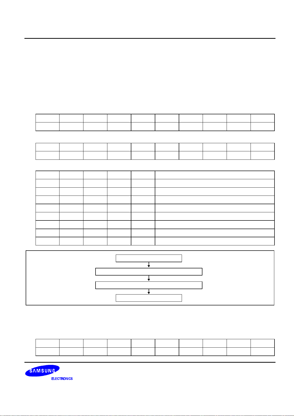
S6B0741 128 SEG / 129 COM DRIVER & CONTROLLER FOR STN LCD
Set N-line Inversion Register
Sets the inverted line number within range of 3 to 33 to improve the display quality by controlling the phase of
the internal LCD AC signal (M) by using the 2-byte instruction.
The DC-bias problem could be occurred if K is even number. So, we recommend customers to set K to be odd
number. K : D/N
D : The number of display duty ratio (D is selectable by customers)
N : N for N-line inversion (N is selectable by customers).
The 1st Instruction
RS RW DB7 DB6 DB5 DB4 DB3 DB2 DB1 DB0
0 0 0 1 0 0 1 1
× ×
The 2nd Instruction
RS RW DB7 DB6 DB5 DB4 DB3 DB2 DB1 DB0
0 0
× × ×
N4 N3 N2 N1 N0
N4 N3 N2 N1 N0 Selected n-line inversion
0 0 0 0 0 0-line inversion (frame inversion)
0 0 0 0 1 3-line inversion
0 0 0 1 0 4-line inversion
0 0 0 1 1 5-line inversion
: : : : : :
1 1 1 0 1 31-line inversion
1 1 1 1 0 32-line inversion
1 1 1 1 1 33-line inversion
Setting N-Line Inversion Start
1st Instruction (Mode Setting)
2nd Instruction (N-Line Inversion Setting)
Setting N-Line Inversion End
Figure 31. Sequence for N-line Inversion
Release N-line Inversion
Returns to the frame inversion condition from the n-line inversion condition.
RS RW DB7 DB6 DB5 DB4 DB3 DB2 DB1 DB0
0 0 1 1 1 0 0 1 0 0
47
Page 52
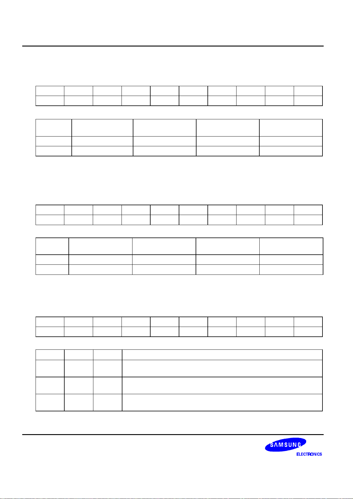
128 SEG / 129 COM DRIVER & CONTROLLER FOR STN LCD S6B0741
Reverse Display ON / OFF
Reverses the display status on LCD panel without rewriting the contents of the display data RAM.
RS RW DB7 DB6 DB5 DB4 DB3 DB2 DB1 DB0
0 0 1 0 1 0 0 1 1 REV
REV
DDRAM data = “00”
– White
DDRAM data = “01”
– Light gray
DDRAM data = “10”
– Dark gray
DDRAM data = “11”
– Dark
0 (normal) White (“00”) Light gray (“01”) Dark gray (“10”) Dark (“ 11” )
1 (reverse) Dark (“ 11” ) Dark gray (“10”) Light gray (“01”) White (“00”)
Entire Display ON / OFF
Forces the whole LCD points to be turned on regardless of the contents of the display data RAM. At this time,
the contents of the display data RAM are held. This instruction has priority over the Reverse Display ON / OFF
instruction.
RS RW DB7 DB6 DB5 DB4 DB3 DB2 DB1 DB0
0 0 1 0 1 0 0 1 0 EON
EON
DDRAM data = “00”
– White
DDRAM data = “01”
– Light gray
DDRAM data = “10”
– Dark gray
DDRAM data = “11”
– Dark
0 (normal) White (“ 00” ) Light gray (“ 01” ) Dark gray (“10”) Dark (“ 11” )
1 (entire) Dark (“11”) Dark (“11”) Dark (“ 11” ) Dark (“11” )
Power Control
Selects one of eight power circuit functions by using 3-bit register. An external power supply and part of internal
power supply functions can be used simultaneously.
48
RS RW DB7 DB6 DB5 DB4 DB3 DB2 DB1 DB0
0 0 0 0 1 0 1 VC VR VF
VC VR VF Status of internal power supply circuits
0
1
0
1
0
1
Internal voltage converter circuit is OFF
Internal voltage converter circuit is ON
Internal voltage regulator circuit is OFF
Internal voltage regulator circuit is ON
Internal voltage follower circuit is OFF
Internal voltage follower circuit is ON
Page 53
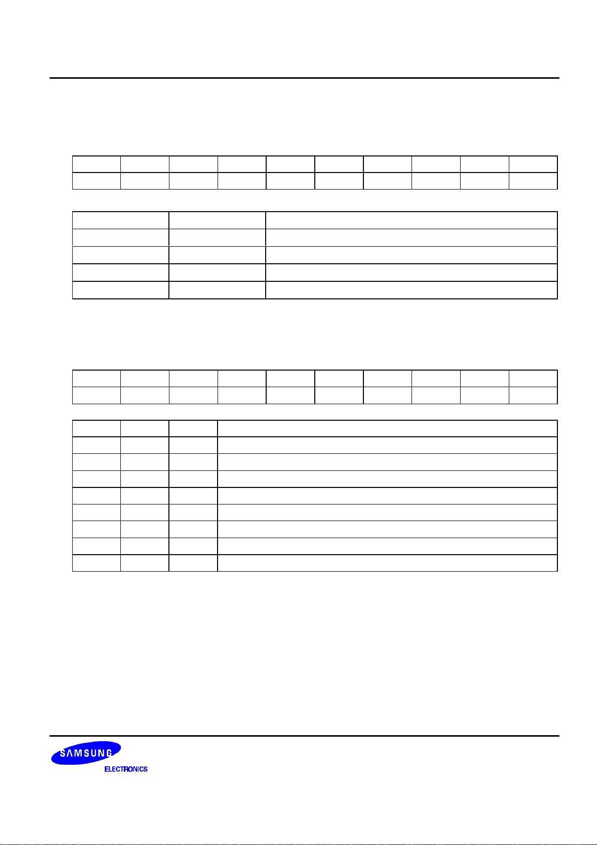
S6B0741 128 SEG / 129 COM DRIVER & CONTROLLER FOR STN LCD
Select DC-DC Step-up
Selects one of 4 DC-DC step-up to reduce the power consumption by this instruction. It is very useful to realize
the partial display function.
RS RW DB7 DB6 DB5 DB4 DB3 DB2 DB1 DB0
0 0 0 1 1 0 0 1 DC1 DC0
DC1 DC0 Selected DC-DC converter circuit
0 0 3 times boosting circuit
0 1 4 times boosting circuit
1 0 5 times boosting circuit
1 1 6 times boosting circuit
Select Regulator Resistor
Selects resistance ratio of the internal resistor used in the internal voltage regulator. See voltage regulator
section in power supply circuit. Refer to the table 14.
RS RW DB7 DB6 DB5 DB4 DB3 DB2 DB1 DB0
0 0 0 0 1 0 0 R2 R1 R0
R2 R1 R0 1+ (Rb / Ra)
0 0 0 2.3
0 0 1 3.0
0 1 0 3.7
0 1 1 4.4
1 0 0 5.1
1 0 1 5.8
1 1 0 6.5
1 1 1 7.2
49
Page 54
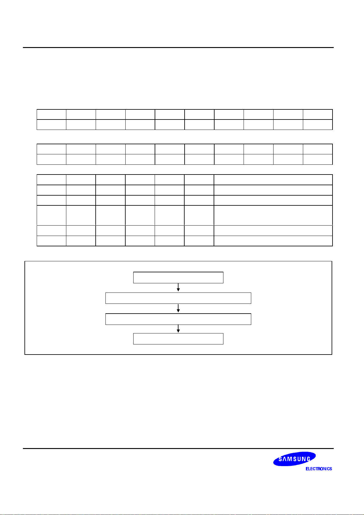
128 SEG / 129 COM DRIVER & CONTROLLER FOR STN LCD S6B0741
Set Electronic Volume Register
Consist of 2-byte Instructions
The 1st instruction set Reference Voltage mode, the 2nd one updates the contents of reference voltage register.
After second instruction, Reference Voltage mode is released.
The 1st Instruction: Set Reference Voltage Select Mode
RS RW DB7 DB6 DB5 DB4 DB3 DB2 DB1 DB0
0 0 1 0 0 0 0 0 0 1
The 2nd Instruction: Set Reference Voltage Register
RS RW DB7 DB6 DB5 DB4 DB3 DB2 DB1 DB0
0 0
× ×
EV5 EV4 EV3 EV2 EV1 EV0
EV5 EV4 EV3 EV2 EV1 EV0
Reference voltage parameter (α)
0 0 0 0 0 0 0
0 0 0 0 0 1 1
:
:
:
:
:
:
:
:
:
:
:
:
1 1 1 1 1 0 62
1 1 1 1 1 1 63
Setting Reference Voltage Start
1st Instruction for Mode Setting
2nd Instruction for Register Setting
:
:
50
Setting Reference Voltage End
Figure 32. Sequence for Setting the Electronic Volume
Page 55
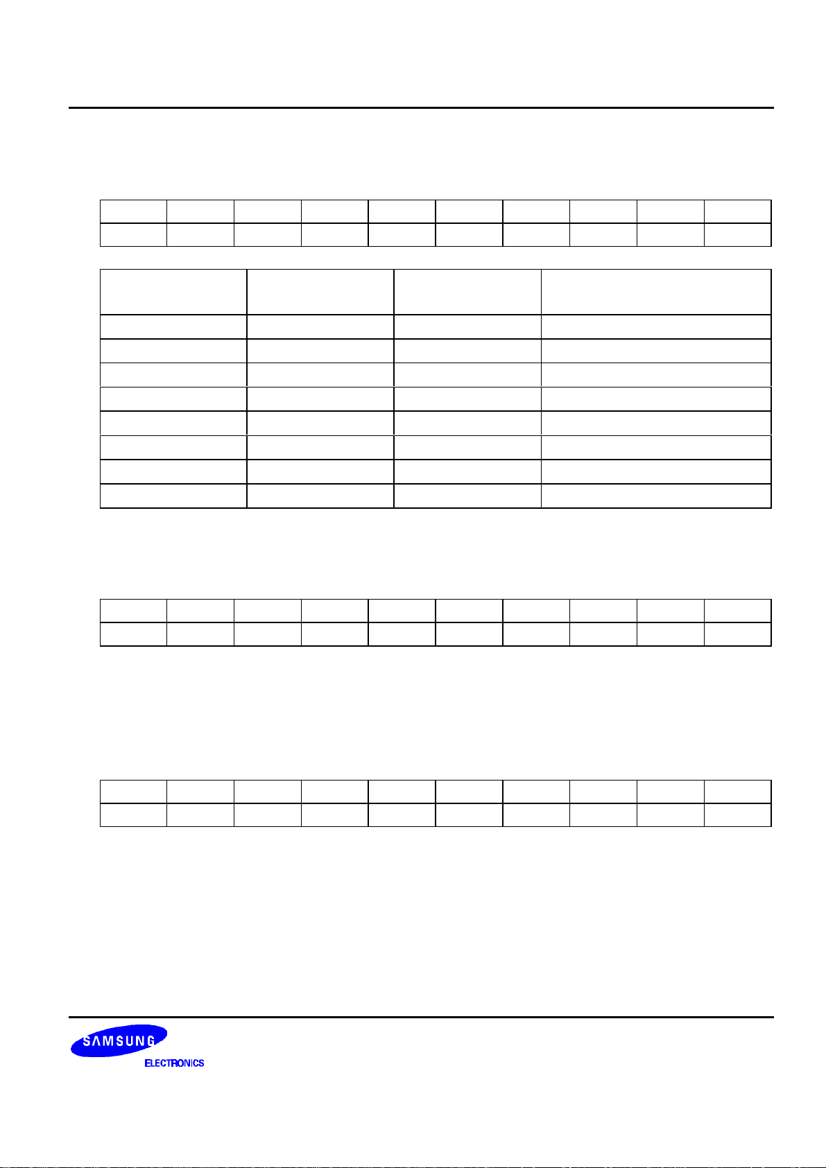
S6B0741 128 SEG / 129 COM DRIVER & CONTROLLER FOR STN LCD
Select LCD Bias
Selects LCD bias ratio of the voltage required for driving the LCD.
RS RW DB7 DB6 DB5 DB4 DB3 DB2 DB1 DB0
0 0 0 1 0 1 0 B2 B1 B0
B2 B1 B0 LCD bias
0 0 0 1/5
0 0 1 1/6
0 1 0 1/7
0 1 1 1/8
1 0 0 1/9
1 0 1 1/10
1 1 0 1/11
1 1 1 1/12
SHL Select
COM output scanning direction is selected by this instruction which determines the LCD driver output status.
RS RW DB7 DB6 DB5 DB4 DB3 DB2 DB1 DB0
0 0 1 1 0 0 SHL
× × ×
× : Don’ t care
SHL = 0: normal direction (COM0 → COM127)
SHL = 1: reverse direction (COM127 → COM0)
ADC Select
Changes the relationship between RAM column address and segment driver. The direction of segment driver
output pins could be reversed by software. This makes IC layout flexible in LCD module assembly.
RS RW DB7 DB6 DB5 DB4 DB3 DB2 DB1 DB0
0 0 1 0 1 0 0 0 0 ADC
ADC = 0: normal direction (SEG0 → SEG127)
ADC = 1: reverse direction (SEG127 → SEG0)
51
Page 56
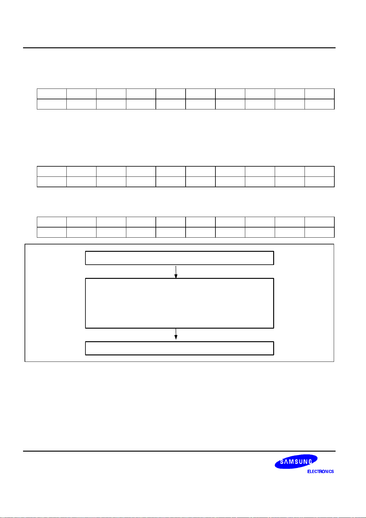
128 SEG / 129 COM DRIVER & CONTROLLER FOR STN LCD S6B0741
Oscillator ON Start
This instruction enables the built-in oscillator circuit.
RS RW DB7 DB6 DB5 DB4 DB3 DB2 DB1 DB0
0 0 1 0 1 0 1 0 1 1
Power Save
The S6B0741 enters the Power Save status to reduce the power consumption to the static power consumption
value and returns to the normal operation status by the following instructions.
Set Power Save Mode
RS RW DB7 DB6 DB5 DB4 DB3 DB2 DB1 DB0
0 0 1 0 1 0 1 0 0 P
P = 0: normal mode
P = 1: sleep mode
Release Power Save Mode
RS RW DB7 DB6 DB5 DB4 DB3 DB2 DB1 DB0
0 0 1 1 1 0 0 0 0 1
Set Power Save Mode (Sleep Mode)
Sleep Mode
Oscillator Circuits: OFF
LCD Power Supply Circuits: OFF
All COM / SEG Output Level: VSS
Consumption Current < 2uA
Release Power Save Mode (Sleep Mode)
Figure 33. Power Save Routine
52
Page 57
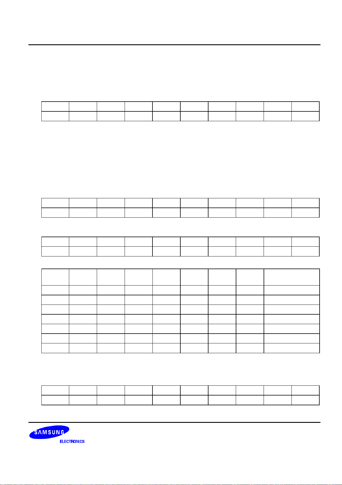
S6B0741 128 SEG / 129 COM DRIVER & CONTROLLER FOR STN LCD
Reset
This instruction Resets initial display line, column address, page address, and common output status select to
their initial status, but dose not affect the contents of display data RAM. This instruction cannot initialize the LCD
power supply, which is initialized by the RESETB pin.
RS RW DB7 DB6 DB5 DB4 DB3 DB2 DB1 DB0
0 0 1 1 1 0 0 0 1 0
Set Data Direction & Display Data Length (3-Pin SPI Mode)
Consists of 2 bytes instruction.
This command is used in 3-Pin SPI mode only(PS0 = ”L” and PS1 = ”L”). It will be two continuous commands,
the first byte control the data direction(write mode only) and inform the LCD driver the second byte will be
number of data bytes will be write. When RS is not used, the Display Data Length instruction is used to indicate
that a specified number of display data bytes are to be transmitted. The next byte after the display data string is
handled as command data.
The 1st Instruction: Set Data Direction (Only Write Mode)
RS RW DB7 DB6 DB5 DB4 DB3 DB2 DB1 DB0
x x 1 1 1 0 1 0 0 0
The 2nd Instruction: Set Display Data Length (DDL) Register
RS RW DB7 DB6 DB5 DB4 DB3 DB2 DB1 DB0
x x D7 D6 D5 D4 D3 D2 D1 D0
D7 D6 D5 D4 D3 D2 D1 D0
0 0 0 0 0 0 0 0 1
0 0 0 0 0 0 0 1 2
0 0 0 0 0 0 1 0 3
: : : : : : : : :
1 1 1 1 1 1 0 1 254
1 1 1 1 1 1 1 0 255
1 1 1 1 1 1 1 1 256
NOP
No operation
Display Data
Length
RS RW DB7 DB6 DB5 DB4 DB3 DB2 DB1 DB0
0 0 1 1 1 0 0 0 1 1
53
Page 58
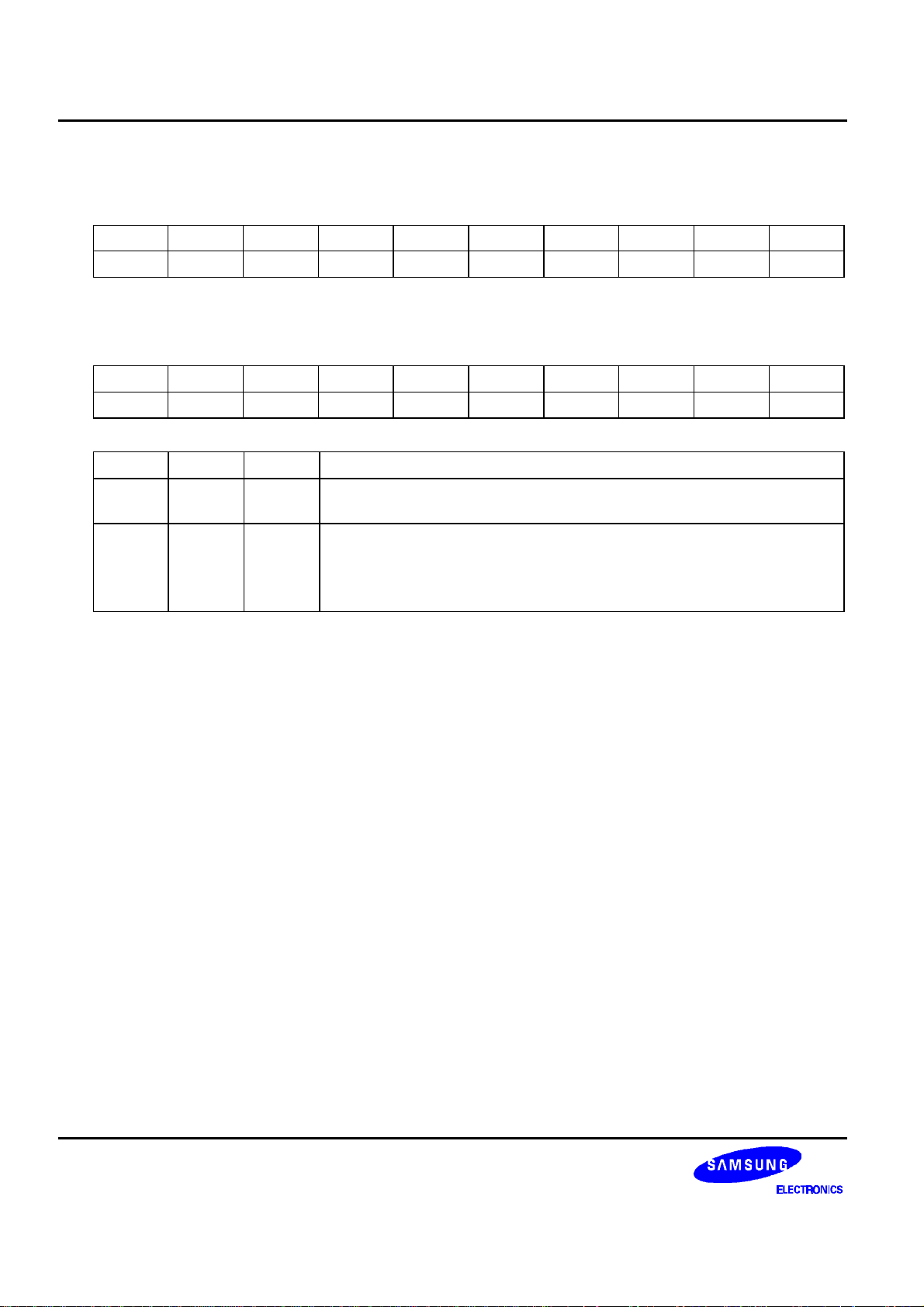
128 SEG / 129 COM DRIVER & CONTROLLER FOR STN LCD S6B0741
Test Instruction
This instruction is for testing IC. Please do not use it.
RS RW DB7 DB6 DB5 DB4 DB3 DB2 DB1 DB0
0 0 1 1 1 1
Set PWM & FRC mode
Selects 3/4 FRC and 9 / 12 / 15 PWM
RS RW DB7 DB6 DB5 DB4 DB3 DB2 DB1 DB0
0 0 1 0 0 1 0 FRC PWM1 PWM0
FRC PWM1 PWM0 Status of PWM & FRC
0
1
0
0
1
1
× × × ×
4FRC
3FRC
0
1
0
1
9PWM
9PWM
12PWM
15PWM
54
Page 59
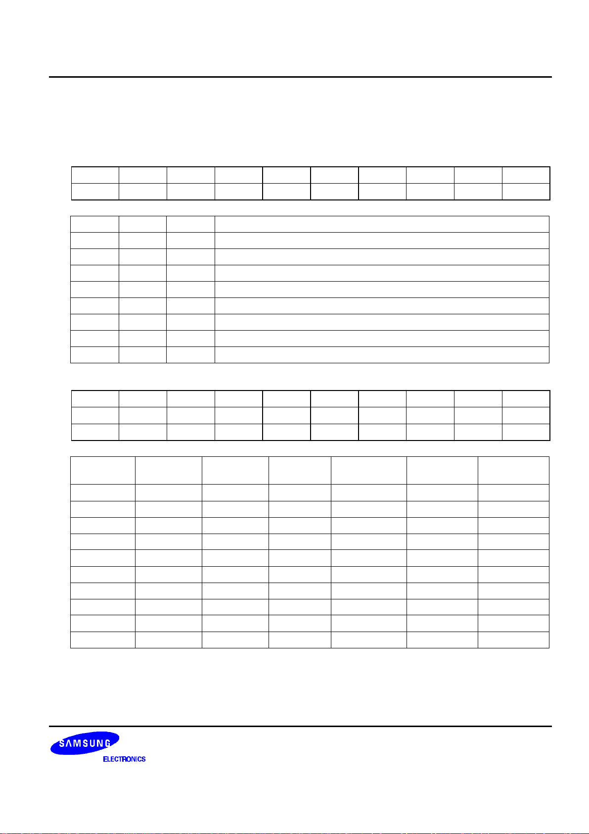
S6B0741 128 SEG / 129 COM DRIVER & CONTROLLER FOR STN LCD
Set Gray Scale Mode & Register
Consists of 2 bytes instruction. The first byte sets grayscale mode and the second byte updates the contents of
gray scale register without issuing any other instruction.
− Set Gray Scale Mode
RS RW DB7 DB6 DB5 DB4 DB3 DB2 DB1 DB0
0 0 1 0 0 0 1 GM2 GM1 GM0
GM2 GM1 GM0 Description
0 0 0 In case of setting white mode and 1st / 2nd frame
0 0 1 In case of setting white mode and 3rd / 4th frame
0 1 0 In case of setting light gray mode and 1st / 2nd frame
0 1 1 In case of setting light gray mode and 3rd / 4th frame
1 0 0 In case of setting dark gray mode and 1st / 2nd frame
1 0 1 In case of setting dark gray mode and 3rd / 4th frame
1 1 0 In case of setting black mode and 1st / 2nd frame
1 1 1 In case of setting black mode and 3rd / 4th frame
− Set Gray Scale Register
RS RW DB7 DB6 DB5 DB4 DB3 DB2 DB1 DB0
0 0 GB3 GB2 GB1 GB0 GA3 GA2 GA1 GA0
0 0 GD3 GD2 GD1 GD0 GC3 GC2 GC1 GC0
GA3, GB3,
GC3, GD3
GA2, GB2,
GC2, GD2
GA1, GB1,
GC1, GD1
GA0, GB0,
GC0, GD0
Pulse width
(9PWM)
Pulse width
(12PWM)
Pulse width
0 0 0 0 0/9 0/12 0/15
0 0 0 1 1/9 1/12 1/15
: : : : : : :
1 0 0 1 9/9 9/12 9/15
1 0 1 0 0/9 10/12 10/15
1 0 1 1 0/9 11/12 11/15
1 1 0 0 0/9 12/12 12/15
1 1 0 1 0/9 0/12 13/15
1 1 1 0 0/9 0/12 14/15
1 1 1 1 0/9 0/12 15/15
(15PWM)
∗ GA3=WA3,LA3,DA3,BA3 GA2=WA2,LA2,DA2,BA2 GA1=WA1,LA1,DA1,BA1 GA0=WA0,LA0,DA0,BA0
GB3=WB3,LB3,DB3,BB3 GA2=WB2,LB2,DB2,BB2 GA1=WB1,LB1,DB1,BB1 GA0=WB0,LB0,DB0,BB0
GC3=WC3,LC3,DC3,BC3 GA2=WC2,LC2,DC2,BC2 GA1=WC1,LC1,DC1,BC1 GA0=WC0,LC0,DC0,BC0
GD3=WD3,LD3,DD3,BD3 GA2=WD2,LD2,DD2,BD2 GA1=WD1,LD1,DD1,BD1 GA0=WD0,LD0,DD0,BD0
55
Page 60
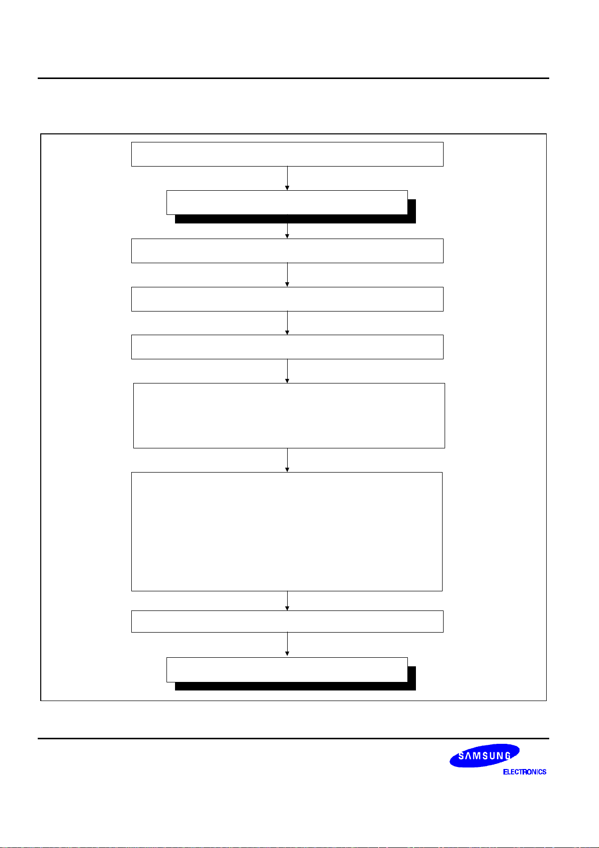
128 SEG / 129 COM DRIVER & CONTROLLER FOR STN LCD S6B0741
End of Initialization
Referential Instruction Set-up Flow: Initializing with the built-in Power Supply Circuits
User System Setup by External Pins
Start of Initialization
Power ON (VDD-VSS) Keeping the RESETB Pin = "L"
Waiting for Stabilizing the Power
RESETB Pin = "H"
User Application Setup by Internal Instructions
[Display Duty Select]
[ADC Select]
[SHL Select]
[COM0 Register Select]
User LCD Power Setup by Internal Instructions
[Oscillator ON]
[DC-DC Step-up Register Select]
[Regulator Resistor Select]
[Electronic Volume Register Select]
[LCD Bias Register Select]
[Gray-scale Select]
[Power Control]
Waiting for Stabilizing the LCD Power Levels
56
Figure 34. Initializing with the Built-in Power Supply Circuits
Page 61
S6B0741 128 SEG / 129 COM DRIVER & CONTROLLER FOR STN LCD
Referential Instruction Set-up Flow: Initializing without the built-in Power Supply Circuits
User System Setup by External Pins
Start of Initialization
Power ON (VDD-VSS) Keeping the RESETB Pin = "L"
Waiting for Stabilizing the Power
RESETB Pin = "H"
Set Power Save
User Application Setup by Internal Instructions
[Display Duty Select]
[ADC Select]
[SHL Select]
[COM0 Register Select]
User LCD Power Setup by Internal Instructions
[Oscillator ON]
Regulator or Follower Register Select
[Gray-scale Select]
[Power Control]
Release Power Save
Waiting for Stabilizing the LCD Power Levels
End of Initialization
Figure 35. Initializing without the Built-in Power Supply Circuits
57
Page 62
128 SEG / 129 COM DRIVER & CONTROLLER FOR STN LCD S6B0741
Referential Instruction Set-up Flow: Data Displaying
End of Initialization
Display Data RAM Addressing by Instruction
[Initial Display Line]
[Set Page Address]
[Set Column Address]
Write Display Data by Instruction
[Display Data Write]
Turn Display ON / OFF Instruction
[Display ON / OFF]
End of Data Display
Figure 36. Data Displaying
Referential Instruction Set-up Flow: Power OFF
Optional Status
Set Power Save by Instruction
Power OFF (VDD-VSS)
End of Power OFF
58
Figure 37. Power OFF
Page 63
S6B0741 128 SEG / 129 COM DRIVER & CONTROLLER FOR STN LCD
Referential Instruction Set-up Flow: Partial Duty Changing
Start of Partial changing
Set Display OFF by Internal
[Display ON / OFF]
Set Sleep Mode by Internal Instruction
[Power Save Mode]
Set Partial Duty by Internal Instructions
[Partial Display Duty Ratio Select]
[Initial Display Line Register]
[COM0 Register Select]
User LCD Power Setup by Internal Instructions
[DC-DC Step-up Register Select]
[Regulator Resistor Select]
[Electronic Volume Register Select]
[LCD Bias Register Select]
[Power Control]
[Gray-scale Select]
Waiting for Discharging the LCD Power Levels
Release Power Save
Waiting for Stabilizing the LCD Power Levels
Write Display Data & Display ON by Internal Instruction
[Display Data Write]
[Display ON / OFF]
End of Partial Changing
Figure 38. Partial Duty Changing
59
Page 64
128 SEG / 129 COM DRIVER & CONTROLLER FOR STN LCD S6B0741
SPECIFICATIONS
ABSOLUTE MAXIMUM RATINGS
Table 18. Absolute Maximum Ratings
(VSS = 0V)
Parameter Symbol Rating Unit
VDD - 0.3 ~ + 7.0 V
V0, VOUT - 0.3 ~ + 17.0 VSupply voltage range
V1, V2, V3, V4 - 0.3 ~ V0 + 0.3 V
External reference voltage VEXT +0.3 ~ VDD
Input voltage range VIN - 0.3 ~ VDD + 0.3 V
Operating temperature range TOPR - 40 ~ + 85 °C
Storage temperature range TSTR - 55 ~ + 125 °C
NOTES:
1. VDD, V0, VOUT, V1 to V4 and VEXT are based on VSS = 0V.
2. Voltages V0 ≥ V1 ≥ V2 ≥ V3 ≥ V4 ≥ VSS must always be satisfied.(VLCD = V0 – VSS)
3. If supply voltage exceeds its absolute maximum range, this LSI may be damaged permanently.
It is desirable to use this LSI under electrical characteristic conditions during general operation.
Otherwise, this LSI may malfunction or reduced LSI reliability may result.
60
Page 65
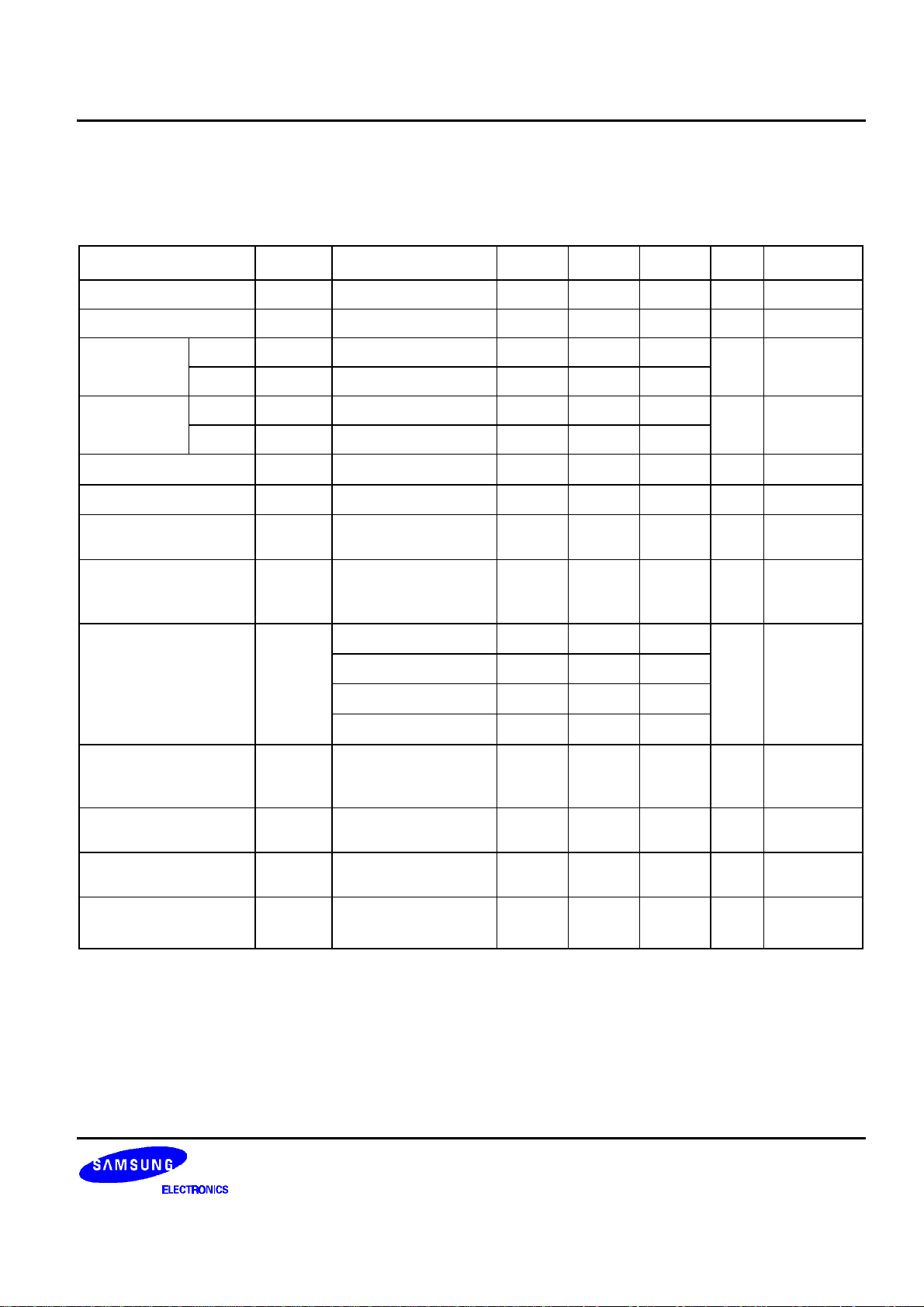
S6B0741 128 SEG / 129 COM DRIVER & CONTROLLER FOR STN LCD
DC CHARACTERISTICS
Table 19. DC Characteristics
(VSS = 0V, VDD = 1.8 to 3.3V, Ta = -40 to 85°C)
Item Symbol Condition Min. Typ. Max. Unit Pin used
Operating voltage (1) VDD 1.8 - 3.3 V VDD (*1)
Operating voltage (2) V0 4.0 - 15.0 V V0 (*2)
Input voltage
Output
voltage
Input leakage current IIL VIN = VDD or VSS - 1.0 - + 1.0
Output leakage current IOZ VIN = VDD or VSS - 3.0 - + 3.0
LCD driver ON
resistance
Operating frequency fFR
Voltage converter
Input voltage
Voltage converter
output voltage
Voltage regulator
operating voltage
Voltage follower
operating voltage
High VIH 0.8VDD - VDD
Low VIL VSS - 0.2VDD
High VOH IOH = -0.5mA 0.8VDD - VDD
Low VOL IOL = 0.5mA VSS - 0.2VDD
RON Ta = 25°C, V0 = 8V - 2.0 3.0 kΩ
Ta = 25°C
1/128 Duty, 9 PWM
REXT = 620kΩ ( *11)
× 3
VCI
VOUT
VOUT 5.4 - 15.0 V VOUT
V0 4.0 - 15.0 V V0 (*8)
voltage conversion
× 4
× 5
× 6
x3 / ×4 / ×5 / ×6
(no-load )
70 85 100 Hz (*7) (*11)
1.8 - 5.0
1.8 - 3.75
1.8 - 3.0
1.8 - 2.5
95 99 - % VOUT
V (*3)
V (*4)
µA
µA
V VCI
(*3)
(*5)
SEGn
COMn (*6)
Reference voltage VREF Ta = 25°C 2.04 2.10 2.16 V (*9)
61
Page 66
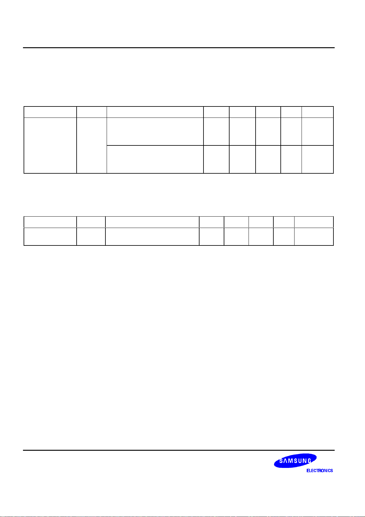
128 SEG / 129 COM DRIVER & CONTROLLER FOR STN LCD S6B0741
Dynamic Current Consumption when The Internal Power Supply is ON
Table 20. Dynamic Current 2 (Internal Power)
(VDD = 3.0V, Ta = 25°C)
Item Symbol Condition Min. Typ. Max. Unit Pin used
V0 - Vss = 12.0V, x5 boosting,
Dynamic current
consumption
duty = 1/128, normal mode
(Display Off)
IDD
V0 - Vss = 12.0V, x5 boosting,
duty = 1/128, normal mode
- 100 150
- 200 300
µΑ
µΑ
(*10)
(*10)
(Display On , Checker Pattern)
Current Consumption during Power Save Mode
Table 21. Power Save Mode Current
(VDD = 3.0V, Ta = 25°C)
Item Symbol Condition Min. Typ. Max. Unit Pin used
Sleep mode
current
IDDS1 During sleep - - 2 µΑ (*10)
62
Page 67

S6B0741 128 SEG / 129 COM DRIVER & CONTROLLER FOR STN LCD
Table 22. The Relationship between Oscillation Frequency and Frame Frequency
Duty ratio Item fCL fosc
1/N
On-chip oscillator circuit is
used
fFR x N fFR x PWM x 2 x N
(fOSC: oscillation frequency, fCL: display clock frequency, fFR: frame frequency, N = 16 to 129)
[* Remark Solves]
*1. Though the wide range of operating voltages is guaranteed, a spike voltage change may affect the voltage
assurance during access from the MPU.
*2. In case of external power supply is applied.
*3. CSB, RS, DB0 to DB7, E_RD, RW_WR, RESETB, PS1, PS0, INTRS and REF
*4. DB0 to DB7
*5. Applies when the DB0 to DB7 pins are in high impedance.
*6. Resistance value when -0.1[mA] is applied during the ON status of the output pin SEGn or COMn.
RON [kΩ] = ∆V[V] / 0.1[mA] (∆V : voltage change when -0.1[mA] is applied in the ON status.)
*7. See Table 23 for the relationship between oscillation frequency and frame frequency.
*8. The voltage regulator circuit adjusts V0 within the voltage follower operating voltage range.
*9. On-chip reference voltage source of the voltage regulator circuit to adjust V0.
*10. Applies to the case where the on-chip oscillation circuit is used and no access is made from the MPU.
The current consumption, when the built-in power supply circuit is ON.
The current flowing through voltage regulation resistors(Rb and Ra) is not included.
It does not include the current of the LCD panel capacity, wiring capacity, etc.
Other conditions are 1/12 bias, 3 FRC, 9 PWM, Frame inversion, Frame freq. = 85HZ, BL=(9,9,9,0),
DG=(6,6,6,0), LG=(3,3,3,0), WH=(0,0,0,0).
*11. Applies when PWM method is used.
When both PWM and FRC method are used, frame frequency should be increased up to more than 130Hz.
So, oscillator resistor value between OSC1 and VDD pin should be reduced.
63
Page 68
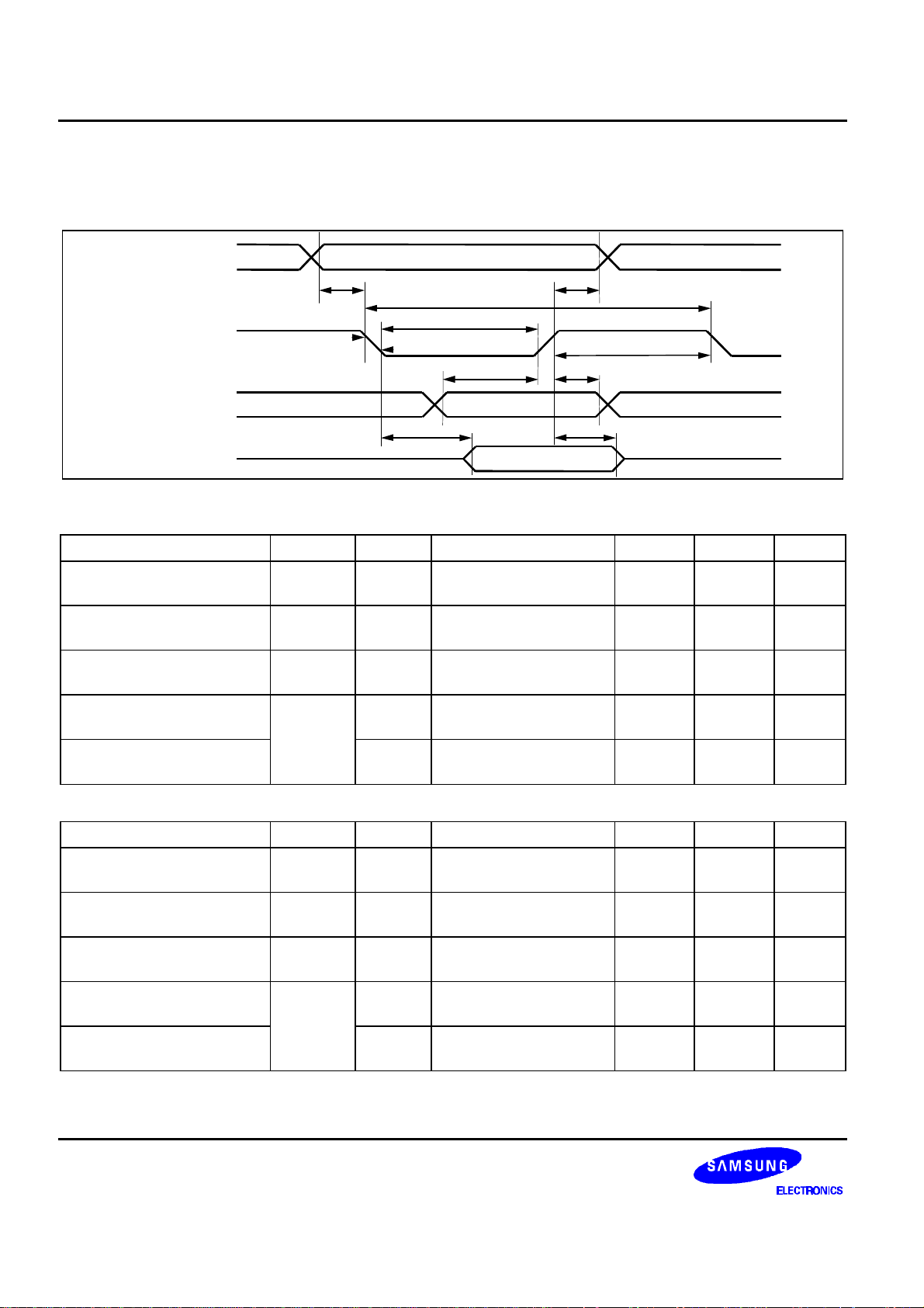
128 SEG / 129 COM DRIVER & CONTROLLER FOR STN LCD S6B0741
AC CHARACTERISTICS
Read / Write Characteristics (8080-series MPU)
RS
t
/RD,
/WR
CSB
DB0 to DB7
( Write )
DB0 to DB7
( Read )
Figure 39. Read / Write Characteristics (8080-series MPU)
Item Signal Symbol Condition Min. Max. Unit
Address setup time
Address hold time
System cycle time for write
System cycle time for read
Pulse width low
Pulse width high
Data setup time
Data hold time
Read access time
Output disable time
0.9VDD
RS
/WR
/RD
DB0
to
DB7
AS80
t
AS80
t
AH80
t
CY80
t
CY80
t
PWL
t
PWH
t
DS80
t
DH80
t
ACC80
t
OD80
0.1V
tACC80
DD
t
PWL
t
CY80
t
DS80
CL = 100 pF
tAH80
t
DH80
t
OD80
t
PWH
(VDD = 1.8V, Ta = -40 ~ +85°C)
0
0
150
330
60
60
40
10
15
10
50
-
-
-
-
-
-
-
-
ns
ns
ns
ns
ns
(VDD = 2.7V, Ta = -40 ~ +85°C)
Item Signal Symbol Condition Min. Max. Unit
Address setup time
Address hold time
System cycle time for write
System cycle time for read
Pulse width low
Pulse width high
Data setup time
Data hold time
Read access time
Output disable time
RS
/WR
/RD
DB0
to
DB7
t
AS80
t
AH80
t
CY80
t
CY80
t
PWL
t
PWH
t
DS80
t
DH80
t
ACC80
t
OD80
CL = 100 pF
0
0
100
166
40
40
30
5
15
10
NOTE: *1. The input signal rise time and fall time (tr, tf) is specified at 15 ns or less.
(tr + tf) < (tCY80 - tPWLW - tPWHW ) for write, (tr + tf) < (tCY80 - tPWLR - tPWHR ) for read
64
50
-
-
-
-
-
-
-
-
ns
ns
ns
ns
ns
Page 69
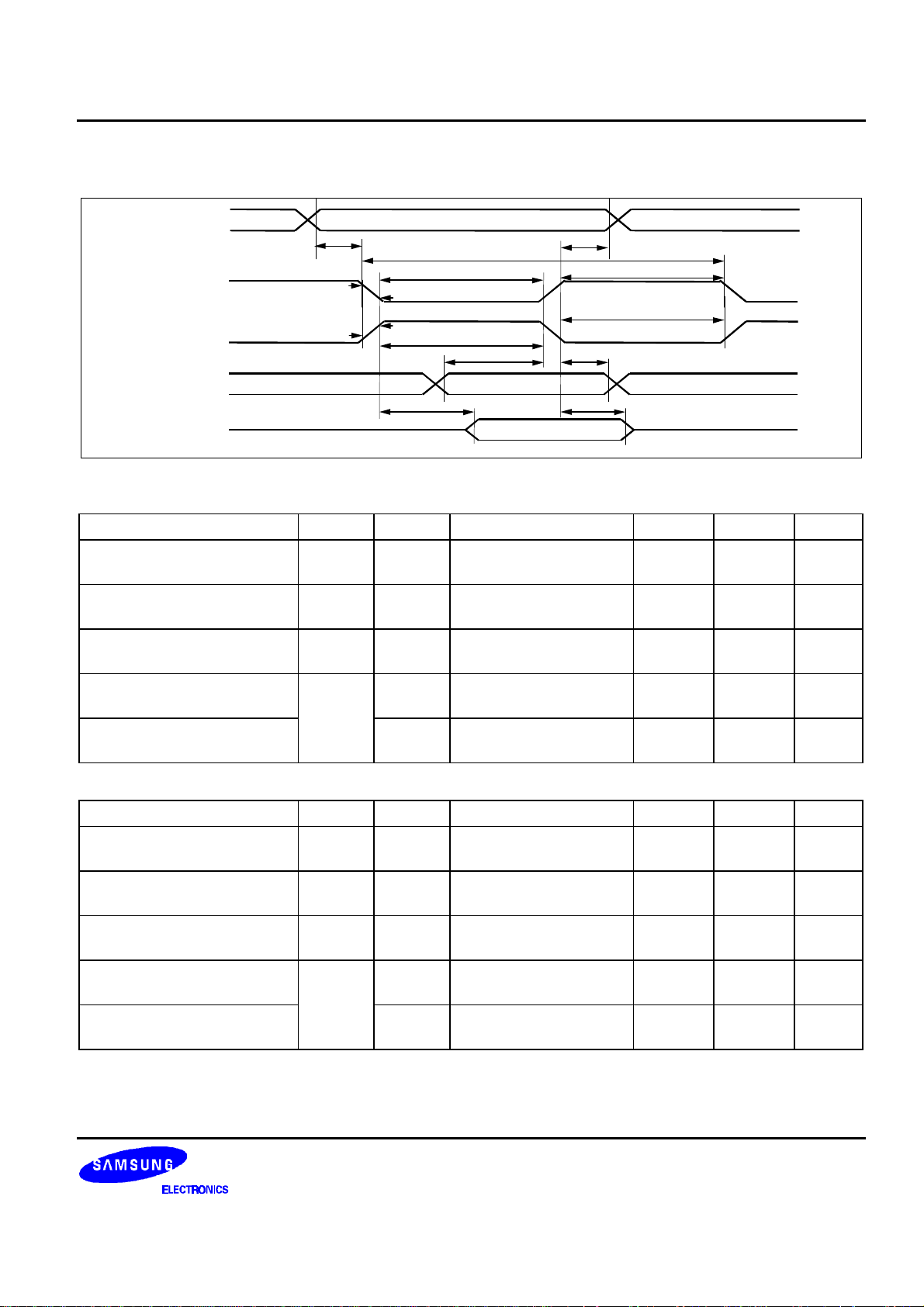
S6B0741 128 SEG / 129 COM DRIVER & CONTROLLER FOR STN LCD
Read / Write Characteristics (6800-series Microprocessor)
RS, R/W
tAH68
tEWH
tEWL
tDH68
tOD68
CSB
DB0 to DB7
( Write )
DB0 to DB7
( Read )
tAS68
0.9VDD
E
0.1VDD
0.1VDD
0.9VDD
tACC68
tCY68
tEWL
tEWH
tDS68
Figure 40. Read / Write Characteristics (6800-series Microprocessor)
(VDD = 1.8V, Ta = -40 ~ +85°C)
Item Signal Symbol Condition Min. Max. Unit
Address setup time
Address hold time
System cycle time for write
System cycle time for read
Enable width high
Enable width low
Data setup time
Data hold time
Read access time
Output disable time
Item Signal Symbol Condition Min. Max. Unit
Address setup time
Address hold time
System cycle time for write
System cycle time for read
Enable width high
Enable width low
Data setup time
Data hold time
Read access time
Output disable time
RS
RW
E_RD
(E)
DB0
to
DB7
RS
RW
E_RD
(E)
DB0
to
DB7
tAS68
tAH68
tCY68
tCY68
tEWH
tEWL
tDS68
tDH68
tACC68
tOD68
tAS68
tAH68
tCY68
tCY68
tEWH
tEWL
tDS68
tDH68
tACC68
tOD68
CL = 100 pF
CL = 100 pF
0
0
150
330
60
60
40
10
15
10
50
-
-
-
-
-
-
-
-
ns
ns
ns
ns
ns
(VDD = 2.7V, Ta = -40 ~ +85°C)
0
0
100
166
40
40
30
5
15
10
50
-
-
-
-
-
-
-
-
ns
ns
ns
ns
ns
NOTE: *1. The input signal rise time and fall time (tr, tf) is specified at 15 ns or less.
(tr + tf) < (t CY68 - tEWHW - tEWLW ) for write, (tr + tf) < (t CY68 - tEWHR - tEWLR ) for read
65
Page 70
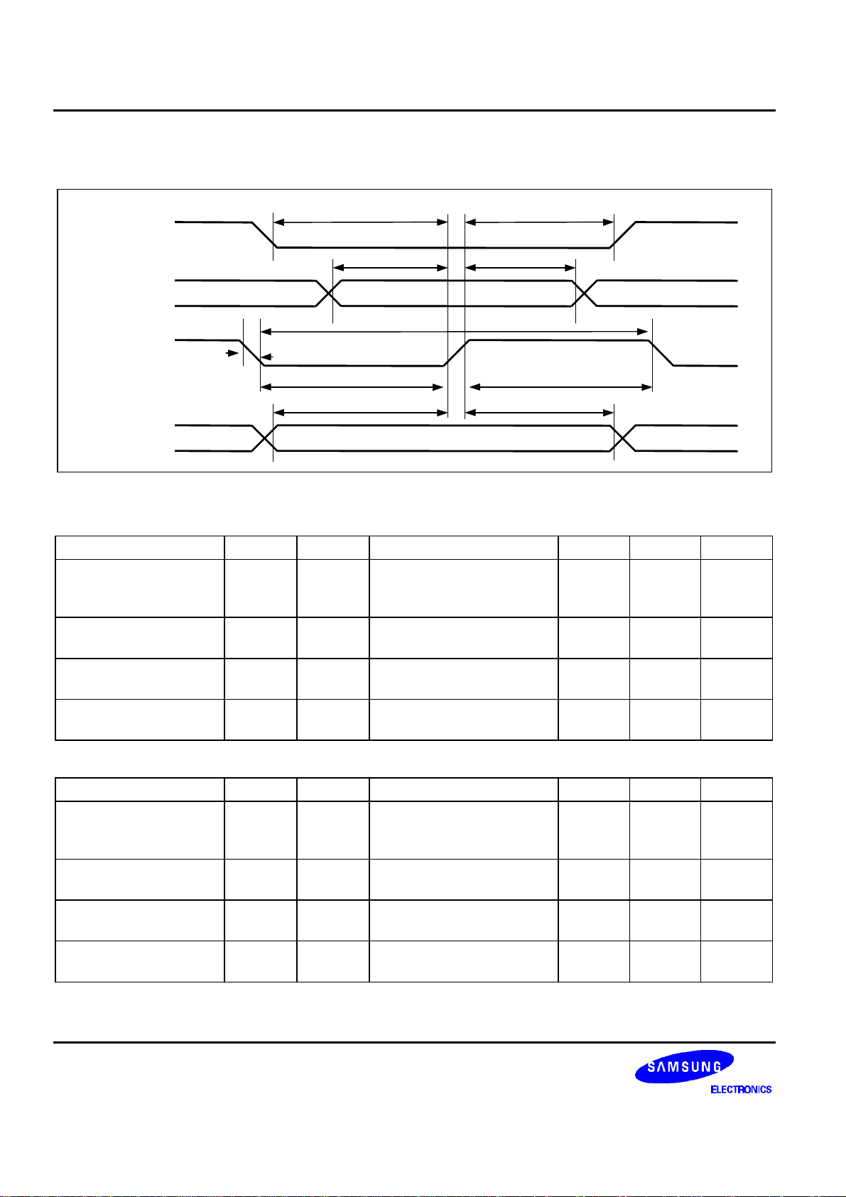
128 SEG / 129 COM DRIVER & CONTROLLER FOR STN LCD S6B0741
Serial Interface Characteristics
tCHStCSS
CSB
tAHStASS
RS
tCYS
DB6
(SCLK)
DB7
(SID)
0.9VDD
0.1VDD
tWLS
tWHS
tDHStDSS
Figure 41. Serial Interface Characteristics
Item Signal Symbol Condition Min. Max. Unit
Serial clock cycle
SCLK high pulse width
SCLK low pulse width
Address setup time
Address hold time
Data setup time
Data hold time
CSB setup time
CSB hold time
Item Signal Symbol Condition Min. Max. Unit
Serial clock cycle
SCLK high pulse width
SCLK low pulse width
Address setup time
Address hold time
Data setup time
Data hold time
CSB setup time
CSB hold time
DB6
(SCLK)
RS
DB7
(SID)
CSB
DB6
(SCLK)
RS
DB7
(SID)
CSB
tCYS
tWHS
tWLS
tASS
tAHS
tDSS
tDHS
tCSS
tCHS
tCYS
tWHS
tWLS
tASS
tAHS
tDSS
tDHS
tCSS
tCHS
(VDD = 1.8V, Ta = -40 ~ +85°C)
111
60
60
60
60
60
60
60
1/2 * tCYS
-
-
ns
-
-
-
-
-
-
-
ns
ns
ns
(VDD = 2.7V, Ta = -40 ~ +85°C)
58.8
30
30
30
30
30
30
30
1/2 * tCYS
-
-
ns
-
-
-
-
-
-
-
ns
ns
ns
NOTE: *1. The input signal rise time and fall time (tr, tf) is specified at 15 ns or less.
66
Page 71
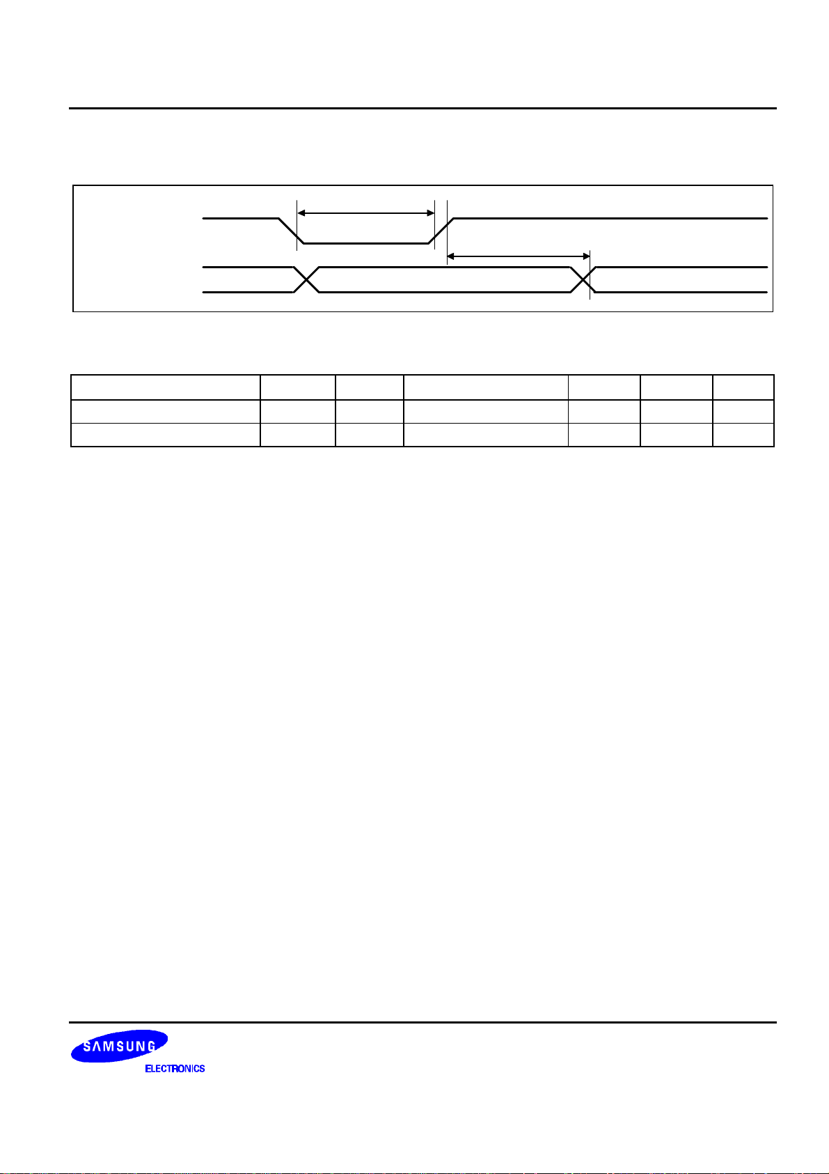
S6B0741 128 SEG / 129 COM DRIVER & CONTROLLER FOR STN LCD
Reset Input Timing
tRW
RESETB
tR
Internal status
Reset completeDuring reset
Figure 42. Reset Input Timing
(VDD = 1.8 ~ 3.3V, Ta = -40 ~ +85°C)
Item Signal Symbol Condition Min. Max. Unit
Reset low pulse width RESETB tRW 1000 - ns
Reset time - tR - 1000 ns
67
Page 72
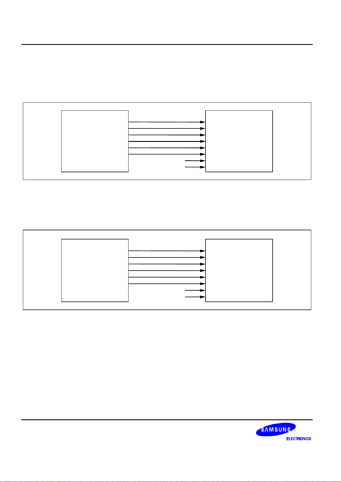
128 SEG / 129 COM DRIVER & CONTROLLER FOR STN LCD S6B0741
REFERENCE APPLICATIONS
MICROPROCESSOR INTERFACE
In Case of Interfacing with 6800-series (PS0 = “H”, PS1 = “H”)
CSB
RS
6800-series
MPU
E
RW
DB0 to DB7
RESETB
DD
V
DD
V
Figure 43. Interfacing with 6800-series (PS0 = “H”, C68 = “H”)
In Case of Interfacing with 8080-series (PS0 = “H”, PS1 = “L”)
CSB
RS
8080-series
MPU
/RD
/WR
DB0 to DB7
RESETB
DD
V
SS
V
CSB
RS
E_RD
RW_WR
DB0 to DB7
RESETB
PS0
PS1
CSB
RS
E_RD
RW_WR
DB0 to DB7
RESETB
PS0
PS1
S6B0741
S6B0741
68
Figure 44. Interfacing with 8080-series (PS0 = “H”, C68 = “L”)
Page 73
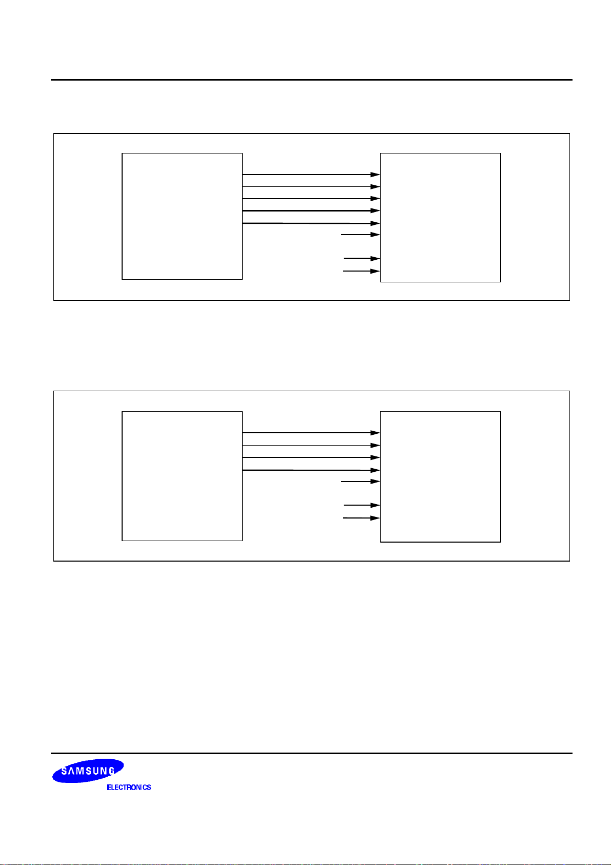
S6B0741 128 SEG / 129 COM DRIVER & CONTROLLER FOR STN LCD
In Case of 4-pin SPI mode (PS0 = "L" , PS1 = "H" )
MPU
Figure 45. Serial Interface (PS0 = “L”, PS1 = “H”)
In Case of 3-pin SPI mode (PS0 = "L" , PS1 = "L" )
MPU
CSB
RS
SID
SCLK
RESETB
OPEN
VSS
V
CSB
SID
SCLK
RESETB
OPEN
V
V
DD
SS
SS
CSB
RS
DB7(SID)
DB6(SCLK)
RESETB
DB0 to DB5
PS0
PS1
CSB
DB7(SID)
DB6(SCLK)
RESETB
DB0 to DB5
PS0
PS1
S6B0741
S6B0741
Figure 46. Serial Interface (PS0 = “L”, PS1 = “L”)
69
Page 74
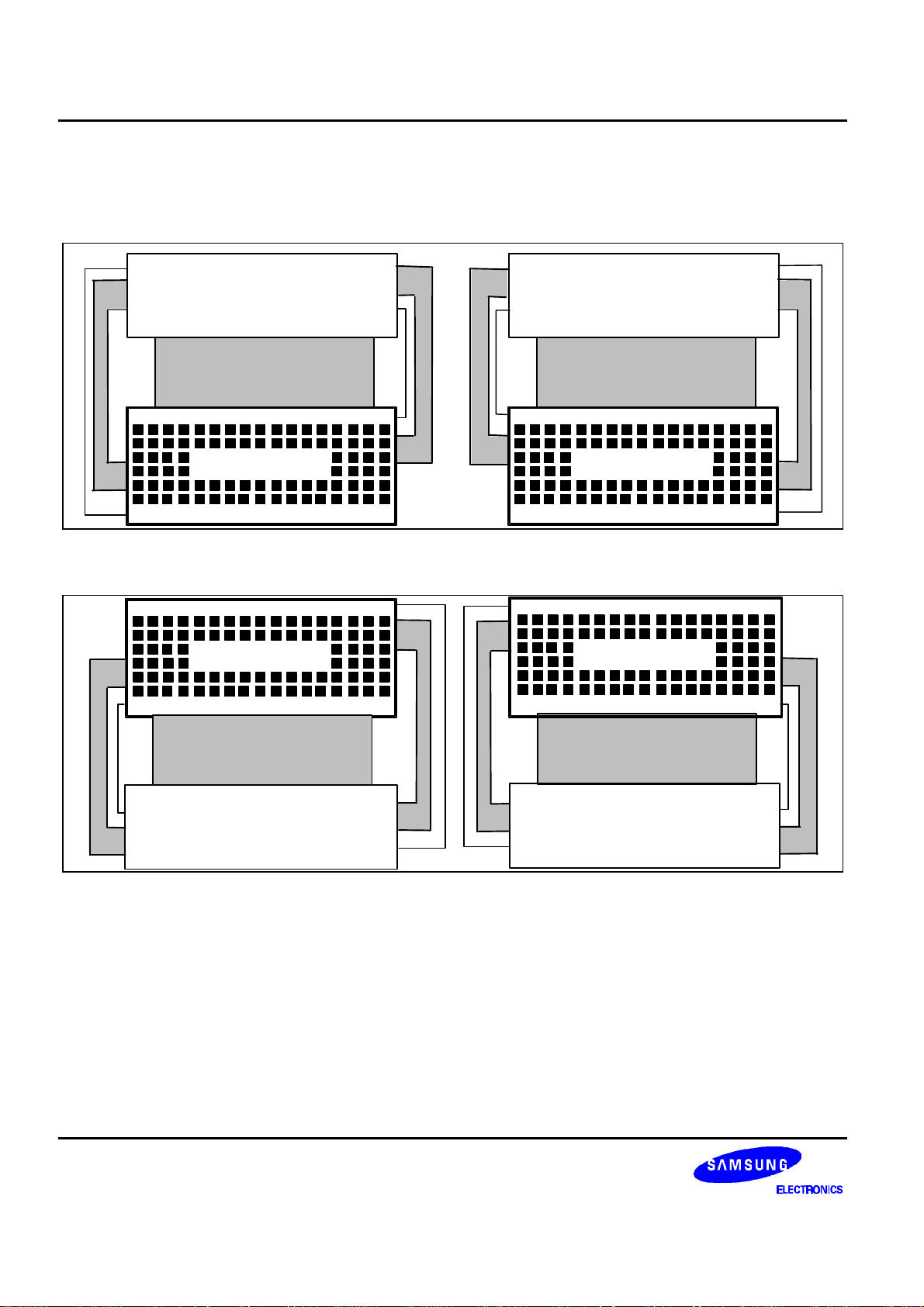
128 SEG / 129 COM DRIVER & CONTROLLER FOR STN LCD S6B0741
CONNECTIONS BETWEEN S6B0741 AND LCD PANEL
Single Chip Configuration (1/129 Duty Configurations)
COMS
COM127
:
COM64
S6B0741
(Bottom View)
SEG127 ........... SEG0
♣ ♦ ♥ ♠ Ξ
129 × 128 pixels
♣ ♦ ♥ ♠ Ξ
COM63
:
COM0
COMS
COM63
:
COM0
COMS
S6B0741
(Top View)
SEG0 ............
♣ ♦ ♥ ♠ Ξ
129 × 128 pixels
♣ ♦ ♥ ♠ Ξ
Figure 47. SHL = 0, ADC = 1 Figure 48. SHL = 0, ADC = 0
♣ ♦ ♥ ♠ Ξ
129 × 128 pixels
♣ ♦ ♥ ♠ Ξ
♣ ♦ ♥ ♠ Ξ
129 × 128 pixels
♣ ♦ ♥ ♠ Ξ
COMS
COM127
:
COM64
70
SEG0 ...........
COMS
COM0
:
COM63
S6B0741
(Bottom View)
COM64
:
COM127
COMS
SEG127 ...........
COM127
:
COM64
COMS
S6B0741
(Top View)
Figure 49. SHL = 1, ADC = 0 Figure 50. SHL = 1, ADC = 1
COMS
COM0
:
COM63
 Loading...