

Page 1

查询S71PL032J80BAW9Z0供应商
S71PL-J Based MCPs
Stacked Multi-Chip Product (MCP) Flash Memory and
RAM 256M/128/64/32 Megabit (16/8/4/2M x 16-bit) CMOS 3.0
Volt-only Simultaneous Operation Page Mode Flash
Memory and 64/32/16/8/4 Megabit (4M/2M/1M/512K/256K x
16-bit) Static RAM/Pseudo Static RAM
Data Sheet
Notice to Readers: The Advance Information status indicates that this
document contains information on one or more products under development
at Spansion LLC. The information is intended to help you evaluate this product.
Do not design in this product without contacting the factory. Spansion LLC
reserves the right to change or discontinue work on this proposed product
without notice.
ADVANCE
INFORMATION
Publication Number S71PL-J_00 Revision B Amendment 3 Issue Date March 17, 2006
Page 2

Advance Information
Notice On Data Sheet Designations
Spansion LLC issues data sheets with Advance Information or Preliminary designations to advise
readers of product information or intended specifications throughout the product life cycle, including development, qualification, initial production, and full production. In all cases, however,
readers are encouraged to verify that they have the latest information before finalizing their design. The following descriptions of Spansion data sheet designations are presented here to highlight their presence and definitions.
Advance Information
The Advance Information designation indicates that Spansion LLC is developing one or more specific products, but has not committed any design to production. Information presented in a document with this designation is likely to change, and in some cases, developmen t on the product
may discontinue. Spansion LLC therefore places the following conditions upon Advance Information content:
“This document contains information on one or more products under dev elopment at Spansion LLC. The
information is intended to help you evaluate this product. Do not design in this product without contacting the factory. Spansion LLC reserves the right to change or discontinue work on this proposed
product without notice.”
Preliminary
The Preliminary designation indicates that the product development has progressed such that a
commitment to production has taken place. This designation covers several aspects of the product life cycle, including product qualification, initial production, and the subsequent phases in the
manufacturing process that occur before full production is achieved. Changes to the technical
specifications presented in a Preliminary document should be expected while keeping these aspects of production under consideration. Spansion places the following conditions upon Preli minary content:
“This document states the current technical specifications regarding the Spansion product(s) described
herein. The Preliminary status of this document indicates that product qualification has been completed,
and that initial production has begun. Due to the phases of the manufacturing process that require
maintaining efficiency and quality, this document may be revised by subsequent versions or modifications due to changes in technical specifications.”
Combination
Some data sheets will contain a combination of products with different designations (Advance Information, Preliminary, or Full Production). This type of document will distinguish these products
and their designations wherever necessary, typically on the first page, the ordering information
page, and pages with DC Characteristics table and AC Erase and Program table (in the table
notes). The disclaimer on the first page refers the reader to the notice on this page.
Full Production (No Designation on Document)
When a product has been in production for a period of time such that no changes or only nominal
changes are expected, the Preliminary designation is removed from the data sheet. Nominal
changes may include those affecting the number of ordering part numbers available, such as the
addition or deletion of a speed option, temperature range, package type, or V
may also include those needed to clarify a description or to correct a typographical error or incorrect specification. Spansion LLC applies the following conditions to documents in this category:
“This document states the current technical specifications regarding the Spansion product(s) described
herein. Spansion LLC deems the products to have been in sufficient production volume such that subsequent versions of this document are not expected t o change. H owever, typographical or specification
corrections, or modifications to the valid combinations offered may occur.”
Questions regarding these document designations may be directed to your local AMD or Fujitsu
sales office.
range. C h a n g e s
IO
ii S71PL-J Based MCPs S71PL-J_00_B3 March 17, 2006
Page 3
S71PL-J Based MCPs
Stacked Multi-Chip Product (MCP) Flash Memory and
RAM 256M/128/64/32 Megabit (16/8/4/2M x 16-bit) CMOS 3.0
Volt-only Simultaneous Operation Page Mode Flash
Memory and 64/32/16/8/4 Megabit (4M/2M/1M/512K/256K x
16-bit) Static RAM/Pseudo Static RAM
Data Sheet
Distinctive Characteristics
MCP Features
Power supply voltage of 2.7 V to 3.1 V
High performance
— 65 ns (65 ns Flash, 70 ns pSRAM)
General Description
The S71PL series is a product line of stacked Multi-Chip Product (MCP) packages and consists
of:
One or more S29PL (Simultaneous Read/Write) Flash memory die
pSRAM or SRAM (See “Referenced Data Sheets” on page 2)
The 256Mb Flash memory consists of two S29PL127J devices. In this case, CE#f2 is used to
access the second Flash and no extra address lines are required.
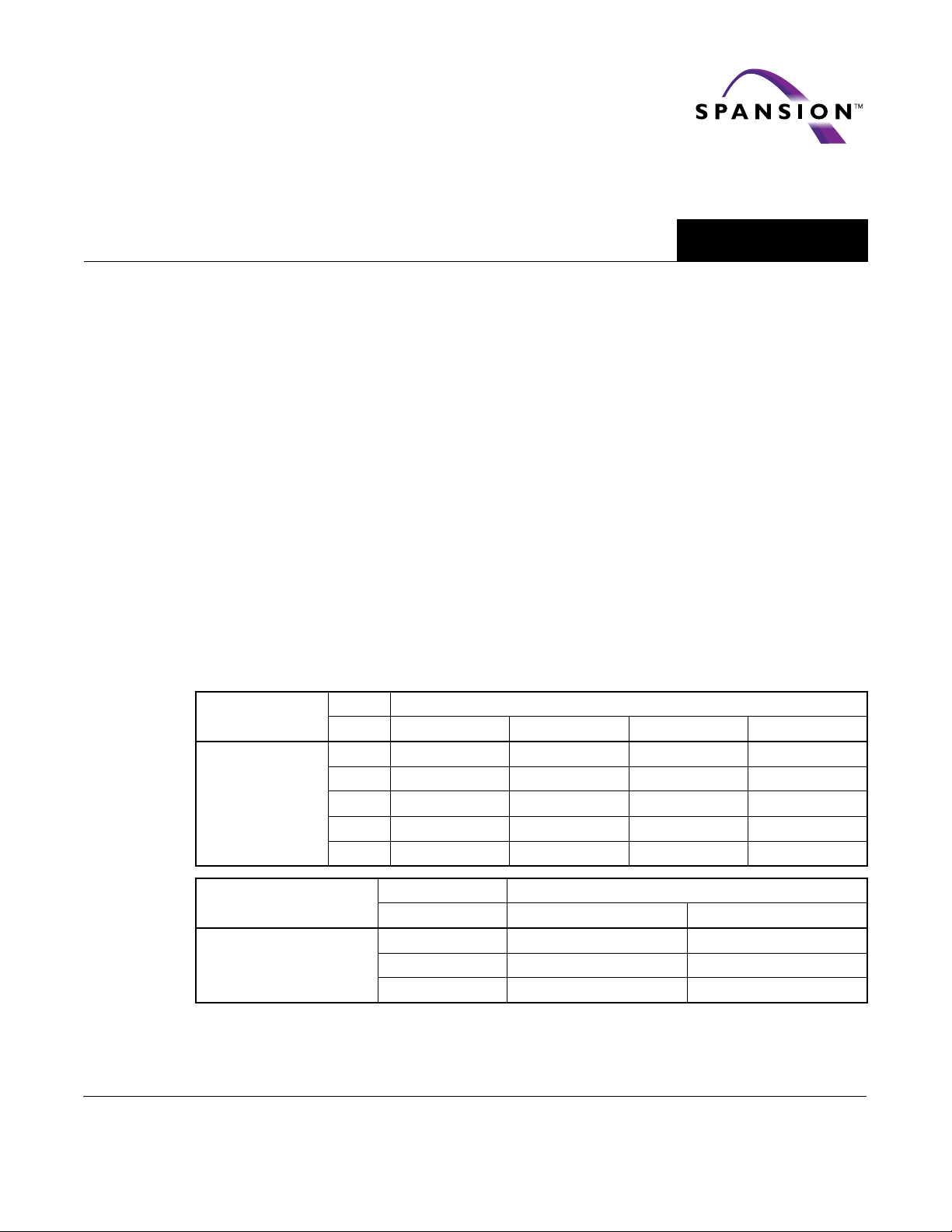
The products covered by this document are listed in the table below:
ADVANCE
INFORMATION
Packages
— 7 x 9 x 1.2mm 56 ball FBGA
— 8 x 11.6 x 1.2mm 64 ball FBGA
— 8 x 11.6 x 1.4mm 84 ball FBGA
Operating Temperature
—–25°C to +85°C
—–40°C to +85°C
Flash Memory Density
32Mb 64Mb 128Mb (Note 2) 256Mb (Note 2)
4 Mb S71PL032J40
8 Mb S71PL032J80 S71PL064J80
pSRAM Density
SRAM Density (Note 1)
Notes:
1. Not recommended for new designs; use pSRAM based MCPs instead.
2. Not recommended for new designs: use S71PL127N and S71PL256N instead.
Publication Number S71PL-J_00 Revision B Amendment 3 Issue Date March 17, 2006
This document contains information on one or more products under deve lopment at Spansion LL C. The information is int ended to he lp you ev aluate this product. Do not design in this product without contacting the factory. Spansion LLC reserves the right to change or discontinue work
on this proposed product without notice.
16 Mb S71PL032JA0 S71PL064JA0
32 Mb S71PL064JB0 S71PL127JB0
64 Mb S71PL127JC0 S71PL254JC0
Flash Memory Density
32Mb 64Mb
4 Mb S71PL032J04
8 Mb S71PL032J08 S71PL064J08
16 Mb S71PL064J0A
Page 4
Advance Information
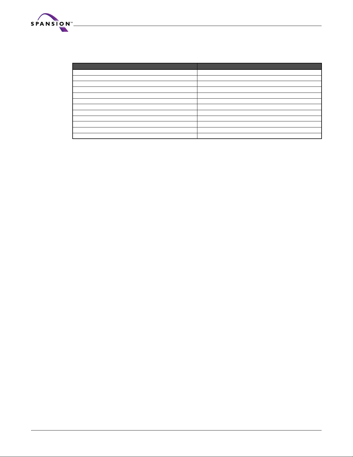
For detailed specifications, please refer to the individual data sheets listed in the following table.
Referenced Data Sheets
Document Publication Identification Number (PID)
S29PL-J S29PL-J_M0
pSRAM Type 1 psram_12
pSRAM Type 2 psram_15
8 Mb pSRAM Type 3 psram_25
16 Mb pSRAM Type 3 psram_06
pSRAM Type 4 psram_18
pSRAM Type 5 psram_21
pSRAM Type 6 psram_14
pSRAM Type 7 psram_13
4Mb/8Mb SRAM Type 1 sram_02
16 Mb SRAM Type 1 sram_06
SRAM Type 4 sram_07
2 S71PL-J Based MCPs S71PL-J_00_B3 March 17, 2006
Page 5
Advance Information
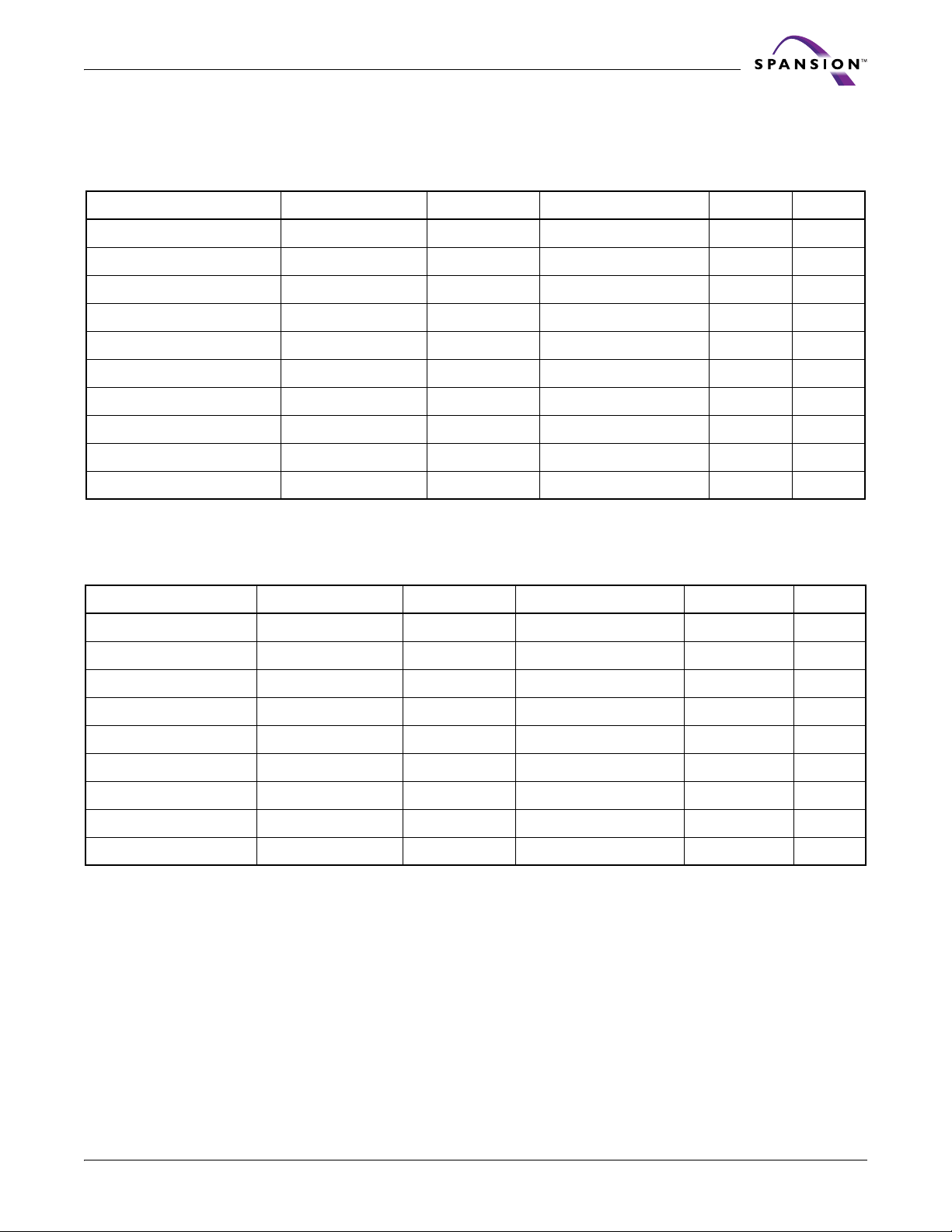
Product Selector Guide
32Mb Flash Memory
Device-Model# Flash Access time (ns) (p)SRAM density (p)SRAM Access time (ns) pSRAM type Package
S71PL032J04-0B 65 4M SRAM 70 SRAM1 TSC056
S71PL032J04-0K 65 4M SRAM 70 SRAM4 TSC056
S71PL032J40-0K 65 4M pSRAM 70 pSRAM4 TLC056
S71PL032J08-0B 65 8M SRAM 70 SRAM1 TSC056
S71PL032J80-0F 65 8M pSRAM 70 pSRAM5 TSC056
S71PL032J80-Q7 65 8M pSRAM 70 pSRAM1 TSC056
S71PL032J80-QF 65 8M pSRAM 70 pSRAM3 TSC056
S71PL032JA0-0K 65 16Mb pSRAM 70 pSRAM1 TSC056
S71PL032JA0-QF 65 16Mb pSRAM 70 pSRAM3 TSC056
S71PL032JA0-0Z 65 16M pSRAM 70 pSRAM7 TLC056
64Mb Flash Memory
Device-Model# Flash Access time (ns) (p)SRAM density (p)SRAM Access time (ns) (p)SRAM type Package
S71PL064J08-0B 65 8M SRAM 70 SRAM1 TLC056
S71PL064J80-0K 65 8M pSRAM 70 pSRAM1 TSC056
S71PL064J0A-0S 65 16M SRAM 70 SRAM1 TLC056
S71PL064JA0-0Z 65 16M pSRAM 70 pSRAM7 TLC056
S71PL064JA0-0B 65 16M pSRAM 70 pSRAM3 TLC056
S71PL064JA0-07 65 16M pSRAM 70 pSRAM1 TLC056
S71PL064JA0-0P 65 16M pSRAM 70 pSRAM7 TLC056
S71PL064JB0-QB 65 32M pSRAM 70 pSRAM2 TLC056
S71PL064JB0-0U 65 32M pSRAM 70 pSRAM6 TLC056
March 17, 2006 S71PL-J_00_B3 S71PL-J Based MCPs 3
Page 6
Advance Information
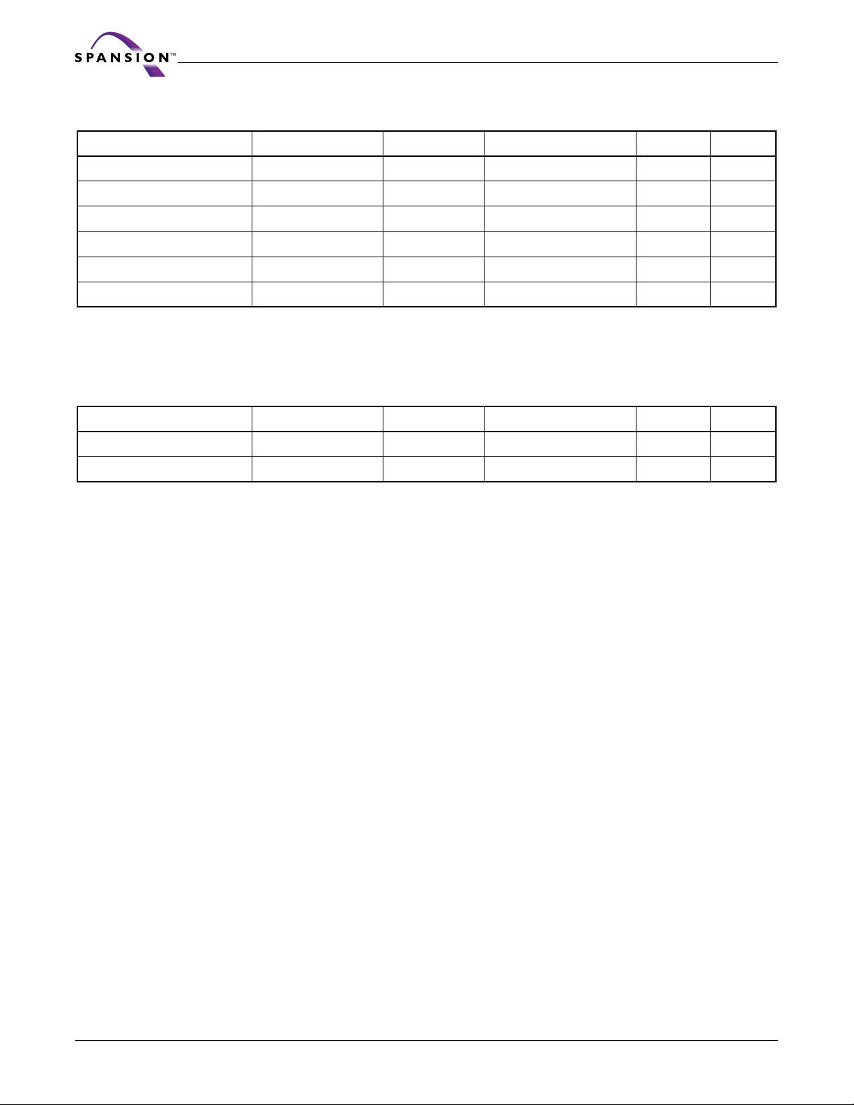
128Mb Flash Memory (Not recommended for new designs; use S71PL127N instead)
Device-Model# Flash Access time (ns) pSRAM density pSRAM Access time (ns) pSRAM type Package
S71PL127JB0-9Z 65 32M pSRAM 70 pSRAM7 TLA064
S71PL127JB0-9U 65 32M pSRAM 70 pSRAM6 TLA064
S71PL127JB0-9B 65 32M pSRAM 70 pSRAM2 TLA064
S71PL127JC0-9B 65 64M pSRAM 70 pSRAM2 TLA064
S71PL127JC0-9Z 65 64M pSRAM 70 pSRAM7 TLA064
S71PL127JC0-9U 65 64M pSRAM 70 pSRAM6 TLA064
256Mb Flash Memory (2xS29PL127J) (Not recommended for new designs: use
S71PL256N instead)
Device-Model# Flash Access time (ns) pSRAM density pSRAM Access time (ns) pSRAM type Package
S71PL254JC0-TB 65 64M pSRAM 70 pSRAM2 FTA084
S71PL254JC0-TZ 65 64M pSRAM 70 pSRAM7 FTA084
4 S71PL-J Based MCPs S71PL-J_00_B3 March 17, 2006
Page 7
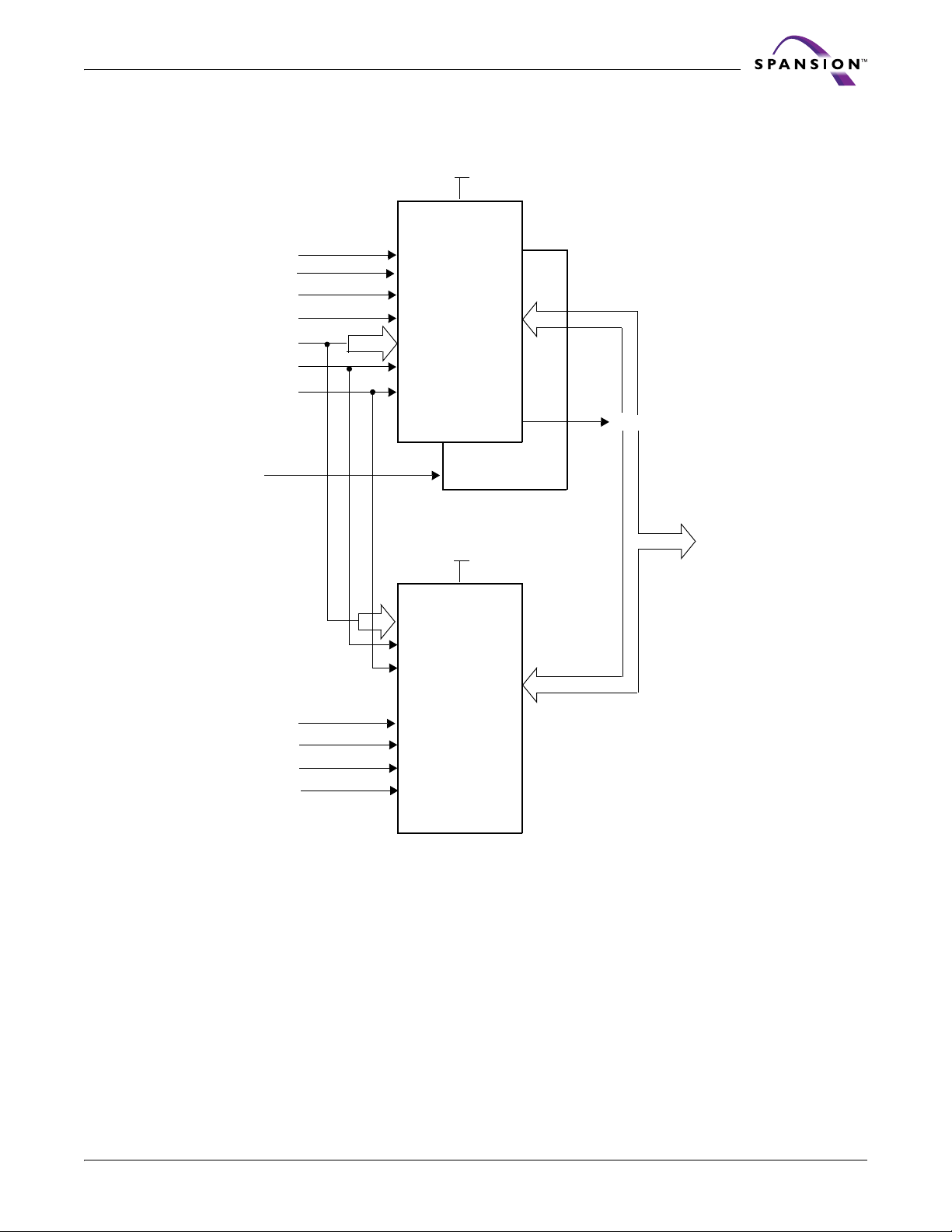
MCP Block Diagram
CE#f1
WP#/ACC
RESET#
Flash-only Address
Shared Address
OE#
WE#
CE#f2
(Note 1)
Advance Information
VCCf
V
CCVCC
Flash 1
V
SS
Flash 2
(Note 2)
RY/BY#
to DQ
DQ
V
CCS
V
CC
15
0
pSRAM/SRAM
IO15-IO
0
CE#s
UB#s
LB#s
CE#
UB#
LB#
CE2
Notes:
1. For 1 Flash + pSRAM, CE#f1=CE#. For 2 Flash + pSRAM, CE#=CE#f1 and CE#f2 is the chip-enable for the second
Flash.
2. For 256Mb only, Flash 1 = Flash 2 = S29PL127J.
March 17, 2006 S71PL-J_00_B3 S71PL-J Based MCPs 5
Page 8
Advance Information
r
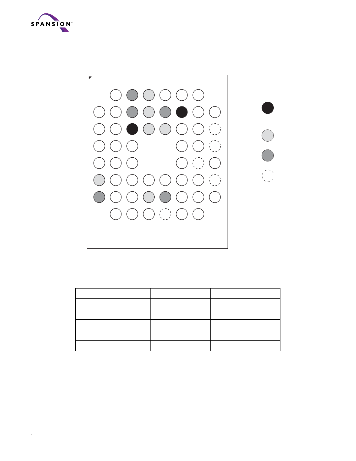
Connection Diagram (S71PL032J)
56-ball Fine-Pitch Ball Grid Array
(Top View, Balls Facing Down)
A3 A5 A6A4 A7A2
A7
B1
A3
C1
A2
D1
A1
E1
A0
F1
CE1#f
G1
B2
A6
C2
A5
D2
A4
E2
VSS
F2
OE#
G2
DQ0CE1#s
H2
DQ8
LB#
B3
UB#
C3
A18
D3
A17
E3
DQ1
F3
DQ9
G3
DQ10
H3
DQ2
WP/ACC
RST#f
RY/BY#
DQ11
B4
C4
DQ3
G4
VCCf
H4
WE#
B5
CE2s
C5
A20
F5F4
DQ4
G5
VCCs
H5
RFU
A8
B6
A19
C6
A9
D6
A10
E6
DQ6
F6
DQ13
G6
DQ12
H6
DQ5
A11
B7
A12
C7
A13
D7
A14
E7
RFU
F7
DQ15
G7
DQ7
H7
DQ14
Notes:
1. May be shared depend i ng o n densi t y.
— A19 is shared for the 16M pSRAM configuration.
— A18 is shared for the 8M pSRAM and above configurations.
2. Connecting all VCC and VSS balls to VCC and VSS is recommended.
B8
A15
C8
RFU
D8
RFU
E8
A16
F8
RFU
G8
VSS
Legend
Shared
(Note 1)
Flash only
RAM only
Reserved fo
Future Use
MCP Flash-only Addresses Shared Addresses
S71PL032JA0 A20 A19-A0
S71PL032J80 A20-A19 A18-A0
S71PL032J08 A20-A19 A18-A0
S71PL032J40 A20-A18 A17-A0
S71PL032J04 A20-A18 A17-A0
6 S71PL-J Based MCPs S71PL-J_00_B3 March 17, 2006
Page 9
Advance Information
r
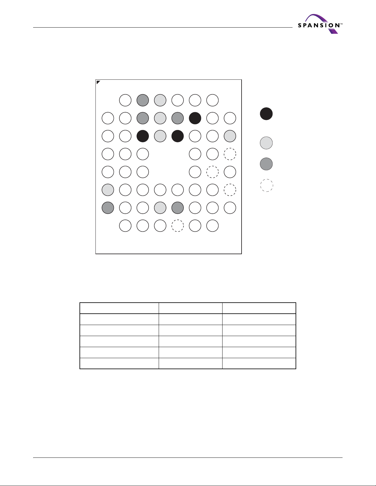
Connection Diagram (S71PL064J)
56-ball Fine-Pitch Ball Grid Array
(Top View, Balls Facing Down)
A3 A5 A6A4 A7A2
A7
LB#
WP/ACC
B2
B1 B8
A3
C1
A2
D1
A1
E1
VSS
A0
F1
CE1#f
OE#
G1
DQ0CE1#s
DQ8
B3
A6
UB#
RST#f
C2
C3
A5
A18
RY/BY#
D2
D3
A4
A17
E2
E3
DQ1
F2
F3
DQ9
G2
G3
DQ10
H2
H3
DQ2
B4
C4
DQ3
G4
VCCf
H4
DQ11
WE#
B5
CE2s
C5
A20
F5F4
DQ4
G5
VCCs
H5
RFU
A8
B6
A19
C6
A9
D6
A10
E6
DQ6
F6
DQ13
G6
DQ12
H6
DQ5
RFU
DQ15
DQ7
DQ14
Notes:
1. May be shared depend i ng o n densi t y.
— A20 is shared for the 32M pSRAM configuration.
— A19 is shared for the 16M pSRAM and above configurations.
— A18 is shared for the 8M pSRAM and above configurations.
2. Connecting all VCC and VSS balls to VCC and VSS is recommended.
A11
B7
A12
C7
A13
D7
A14
E7
F7
G7
H7
A15
C8
A21
D8
RFU
E8
A16
F8
RFU
G8
VSS
Legend
Shared
(Note 1)
Flash only
RAM only
Reserved fo
Future Use
MCP Flash-only Addresses Shared Addresses
S71PL064JB0 A21 A20-A0
S71PL064JA0 A21-A20 A19-A0
S71PL064J0A A21-A20 A19-A0
S71PL064J80 A21-A19 A18-A0
S71PL064J08 A21-A19 A18-A0
March 17, 2006 S71PL-J_00_B3 S71PL-J Based MCPs 7
Page 10
Advance Information
r
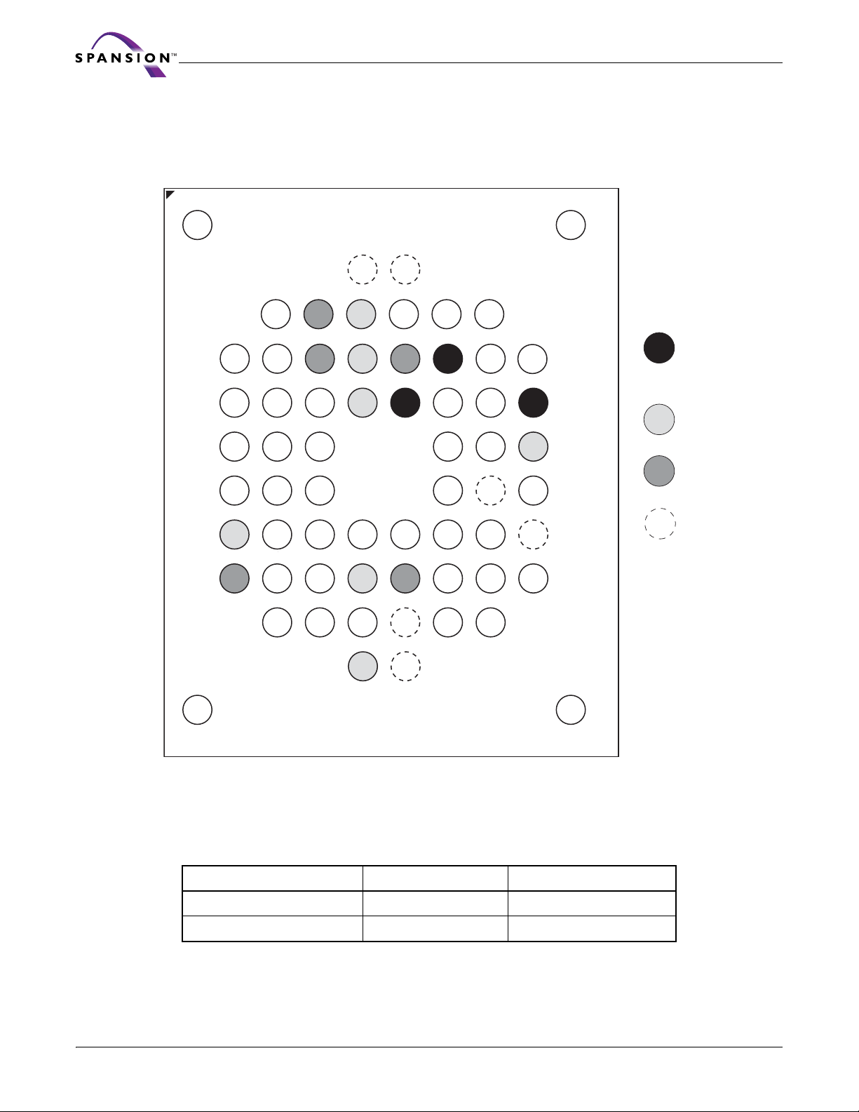
Connection Diagram (S71PL127J)
64-ball Fine-Pitch Ball Grid Array
(Top View, Balls Facing Down)
A1
NC
B6B5
C5
D5
E5
J5
K5
RFU
C6
WE#
D
CE2s
E
A20
H6H5
DQ4
J6
VCCs
K6
RFU
L6L5
RFURFU*
C7
6
A19
6
A10
DQ6
DQ13
DQ12
DQ5
C8
A8
A11
D
E7
A9
F7
G7
H7
J7
K7
D8
7
A12
E8
A13
F8
A14
G8
RFU
H8
DQ15
J8
DQ7
K8
DQ14
RFU
C
C3
A7
D2
A3
G2
A0
H2
CE#f
M1 M10
NC NC
D3
A6
E2
E3
A5
A2
F2
A1
J2
F3
A4
G3
VSS
H3
OE#
J3
DQ0CE1#s
K3
DQ8
4
LB#
D
UB#
E4
A18
F4
A17
G4
DQ1
H4
DQ9
J4
DQ10
K4
DQ2
4
WP/ACC
RST#f
RY/BY#
DQ3
VCCf
DQ11
*See notes below
D9
A15
A21
A22
A16
RFU
VSS
G9
H9
A10
NC
E
9
F9
J9
Legend
Shared
(Note 1)
Flash only
RAM only
Reserved fo
Future Use
Notes:
1. May be shared depend i ng o n densi t y.
— A21 is shared for the 64M pSRAM configuration.
— A20 is shared for the 32M pSRAM and above configurations.
2. A19 is shared for the 16M pSRAM and above configurati o ns .
MCP Flash-only Addresses Shared Addresses
S71PL127JC0 A22 A21-A0
S71PL127JB0 A22-A21 A20- A 0
3. Connecting all V
4. Ball L5 will be V
and VSS balls to Vcc & Vss is recommended.
CC
F in the 84-ball density upgrades. Do not connect to VSS or any other signal.
CC
8 S71PL-J Based MCPs S71PL-J_00_B3 March 17, 2006
Page 11
Advance Information
r
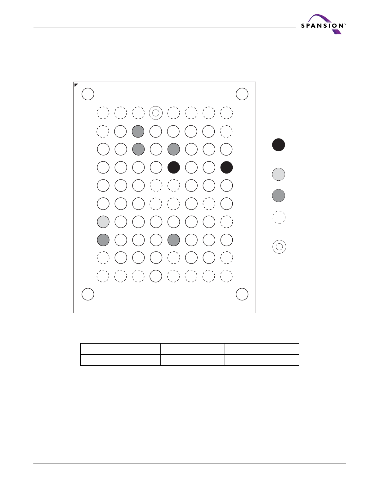
Connection Diagram (S71PL254J)
84-ball Fine-Pitch Ball Grid Array
(Top View, Balls Facing Down)
A1
NC
B2
RFU RFUB7RFUCE#F2
RFU
RFU
C3
C2
RFU
D2
A3
E2
A2
F2
A1
G2
A0
VSS
H2
J2
K2
RFU
L2
RFU
OE#
DQ0CE1#s
DQ8
RFU
CE#f1
M1 M10
NC NC
A7
D3
A6
E3
A5
F3
A4
G3
H3
J3
K3
L3
C4
LB# WE#C7A8WP/ACC
D4
RST#f
UB#
E4
A18
RY/BY#
F4
A17
G4
DQ1
H4
DQ3
DQ9
J4
VCCf
DQ10
K4
DQ2 RFUK7DQ5DQ11
L4
RFU RFUL7RFUVCCf
B6B5
C6C5
D5
D6
CE2s
E5
E
6
A20
H6H5
RFURFU
H6H5
DQ6
RFURFU
H6H5
DQ13
DQ4
J5
J6
DQ12
VCCs
K6K5
L6L5
B4
B3
D7
A19
E7
A9
F7
A10
G7
H7
J7
B8
RFUB9RFU
C8
A11C9RFU
D8
A12
E8
A13
F8
A14
G8
RFU
H8
DQ15
J8
DQ7
K8
DQ14K9RFU
L8
RFUL9RFU
D9
A15
A21
A22
A16
RFU
VSS
A10
NC
E
9
F9
G9
H9
J9
Legend
Shared
(Note 1)
Flash only
RAM only
Reserved fo
Future Use
2nd Flash Only
Notes:
1. May be shared depend i ng o n densi t y.
— A21 is shared for the 64M pSRAM configuration.
— A20 is shared for the 32M pSRAM configuration.
MCP Flash-only Addresses Shared Addresses
S71PL254JC0 A22 A21-A0
2. Connecting all Vcc & Vss balls to Vcc & Vss is recommended.
Special Handling Instructions For FBGA Package
Special handling is required for Flash Memory products in FBGA packages.
Flash memory devices in FBGA packages may be damaged if exposed to ultra-
sonic cleaning methods. The package and/or data integrity may be compromised
if the package body is exposed to temperatures abo ve 150 °C for prolonged peri-
ods of time.
March 17, 2006 S71PL-J_00_B3 S71PL-J Based MCPs 9
Page 12
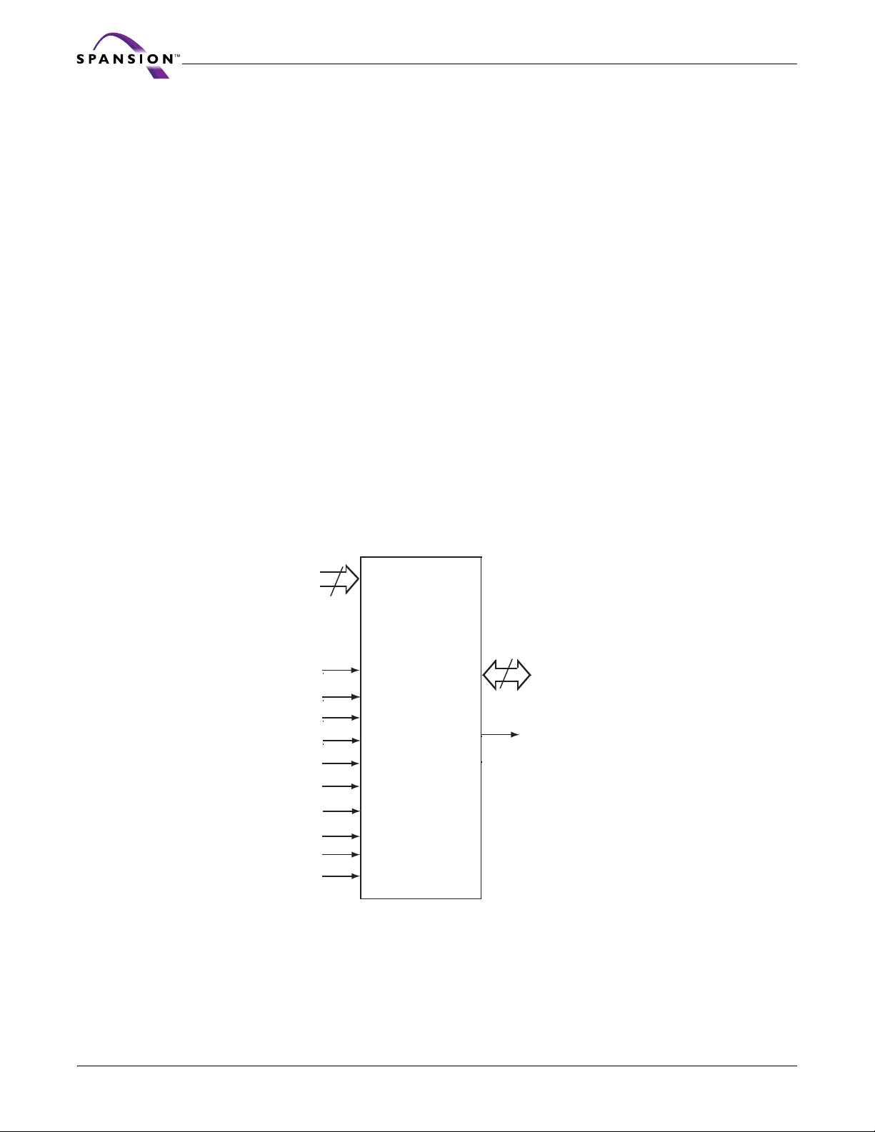
Pin Description
A21–A0 = 22 Address Inputs (Common)
DQ15–DQ0 = 16 Data Inputs/Outputs (Common)
CE1#f = Chip Enable 1 (Flash)
CE#f2 = Chip Enable 2 (Flash)
CE1#ps = Chip Enable 1 (pSRAM)
CE2ps = Chip Enable 2 (pSRAM)
OE# = Output Enable (Common)
WE# = Write Enable (Common)
RY/BY# = Ready/Busy Output (Flash 1)
UB# = Upper Byte Control (pSRAM)
LB# = Lower Byte Control (pSRAM)
RESET# = Hardware Reset Pin, Active Low (Flash 1)
WP#/ACC = Hardware Write Protect/Acceleration Pin (Flash)
f = Flash 3.0 volt-only single power supply (see Product
V
CC
ps = pSRAM Power Supply
V
CC
V
SS
NC = Pin Not Connected Internally
Advance Information
Selector Guide for speed options and voltage supply
tolerances)
= Device Ground (Common)
Logic Symbol
22
A21–A0
CE1#f
CE2#f
CE1#ps
CE2ps
OE#
WE#
WP#/ACC
RESET#
UB#
LB#
16
DQ15–DQ0
R Y/BY#
10 S71PL-J Based MCPs S71PL-J_00_B3 March 17, 2006
Page 13
Advance Information
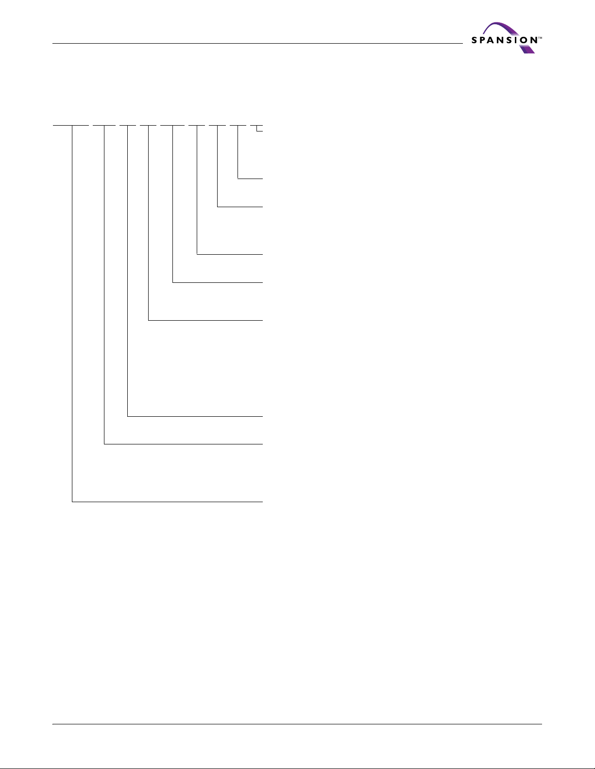
Ordering Information
The order number is formed by a valid combinations of the following:
S71PL 127 J B0 BA W 9 Z 0
PACKING TYPE
0=Tray
2 = 7” Tape and Reel
3 = 13” Tape and Reel
MODEL NUMBER
See the Valid Combinations table.
PACKAGE MODIFIER
0 = 7 x 9mm, 1.2mm height, 56 balls (TLC056 or TSC065)
9 = 8 x 11.6mm, 1.2mm height, 64 balls (TLA064 or TSB064)
T = 8 x 11.6mm, 1.4mm height, 84 balls (FTA084)
TEMPERATURE RANGE
W = Wireless (-25°C to +85°C)
PACKAGE TYPE
BA = Fine-pitch BGA Lead (Pb)-free compliant package
BF = Fine-pitch BGA Lead (Pb)-free package
pSRAM DENSITY
C0 = 64Mb pSRAM
B0 = 32Mb pSRAM
A0 = 16Mb pSRAM
80 = 8Mb pSRAM
40 = 4Mb pSRAM
0A = 16Mb pSRAM
08 = 8Mb SRAM
04 = 4Mb SRAM
PROCESS TECHNOLOGY
J = 110 nm, Floating Gate Technology
FLASH DENSITY
254 = 256Mb
127 = 128Mb
064 = 64Mb
032 = 32Mb
PRODUCT FAMILY
S71PL Multi-chip Product (MCP)
3.0-volt Simultaneous Read/Write, Page Mode Flash Memory and RAM
March 17, 2006 S71PL-J_00_B3 S71PL-J Based MCPs 11
Page 14
Advance Information
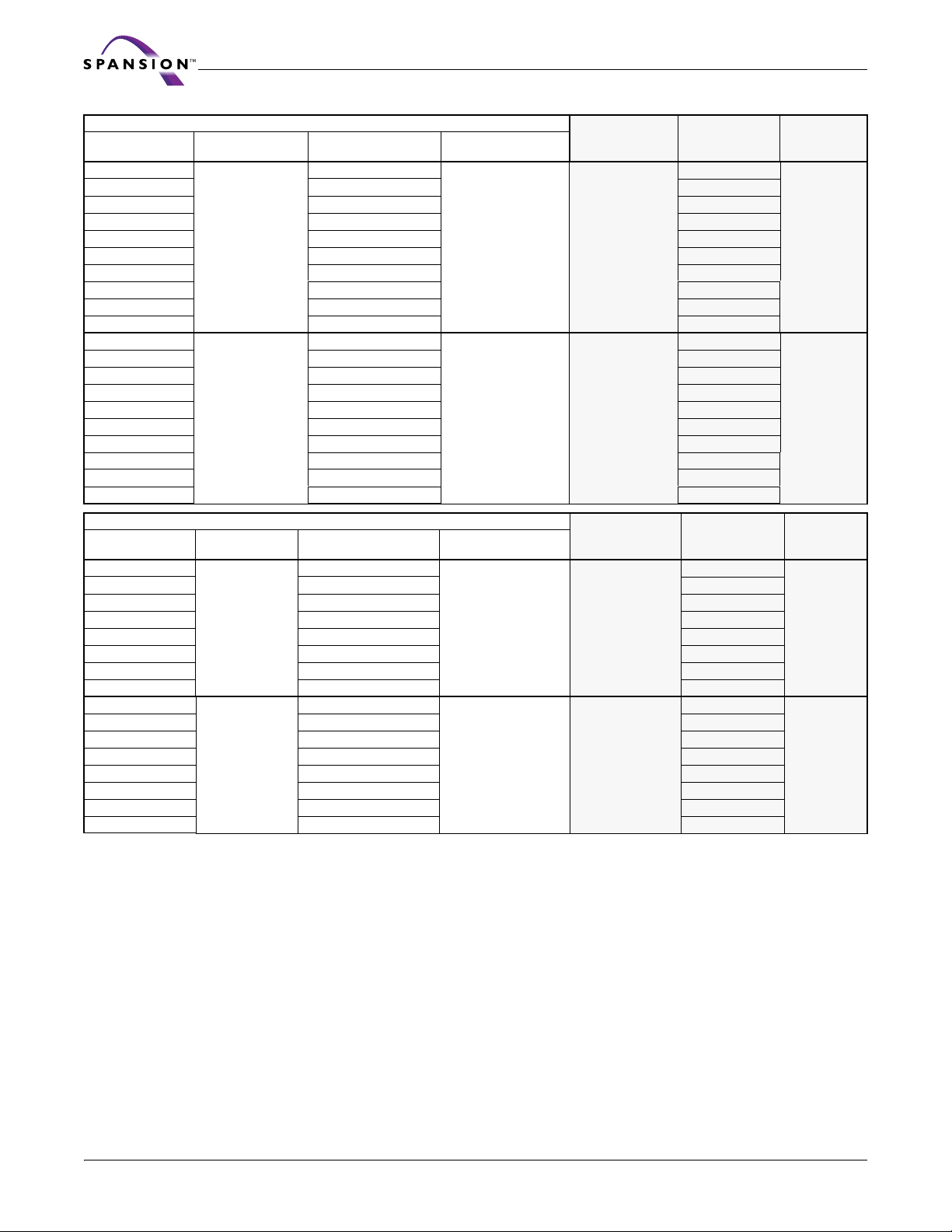
S71PL032J Valid Combinations
Base Ordering
Part Number
S71PL032J04
S71PL032J04 0K
S71PL032J40 0K
S71PL032J80 0F
S71PL032J08 0B SRAM2 / 70
S71PL032J80 Q7
S71PL032J80 QF
S71PL032JA0 07
S71PL032JA0 QF
S71PL032JA0 0Z
S71PL032J04
S71PL032J04 0K
S71PL032J40 0K
S71PL032J80 0F
S71PL032J08 0B
S71PL032J80 Q7
S71PL032J80 QF pSRAM3 / 70
S71PL032JA0 07
S71PL032JA0 QF
S71PL032JA0 0Z
Base Ordering
Part Number
S71PL064J08
S71PL064J80 0K
S71PL064J0A 0S
S71PL064JA0 0B
S71PL064JA0 07
S71PL064JA0 0P
S71PL064JB0 QB
S71PL064JB0 0U
S71PL064J08
S71PL064J80 0K
S71Pl064J0A 0S
S71PL064JA0 0B
S71PL064JA0 07
S71PL064JA0 0P
S71PL064JB0 QB
S71PL064JB0 0U
Notes:
1. Type 0 is standard. Specify other options as required.
2. BGA package marking omits leading “S” and packing type
designator from ordering part number.
Package &
Temperature
BAW
BFW
S71PL064J Valid Combinations
Package &
Temperature
BAW
BFW
Package Modifier/
Model Number Packing Type
Package Modifier/
Model Number Packing Type
0B
0B
0B
0B
0, 2, 3 (Note 1)
0, 2, 3 (Note 1)
0, 2, 3 (Note 1)
0, 2, 3 (Note 1)
Valid Combinations list configuratio ns planned to be sup ported in volume for this device. Consult your local sales office to confirm availability of specific valid combinations and to check on newly released
combinations.
Speed Options
(ns)
65
65
Speed Options
(ns)
65
65
Valid Combinations
(p)SRAM
Type/Access
Time (ns)
SRAM2 / 70
SRAM4 / 70
pSRAM4 / 70
pSRAM5 / 70
pSRAM1 / 70
pSRAM3 / 70
pSRAM1 / 70
pSRAM3 / 70
pSRAM2 / 70
SRAM2 / 70
SRAM4 / 70
pSRAM4 / 70
pSRAM5 / 70
SRAM2 / 70
pSRAM1 / 70
pSRAM1 / 70
pSRAM3 / 70
pSRAM2 / 70
(p)SRAM Type/
Access Time
SRAM1 / 70
pSRAM1 /70
SRAM1 / 70
pSRAM3 / 70
pSRAM1 / 70
pSRAM7 / 70
pSRAM2 / 70
pSRAM6 / 70
SRAM1 / 70
pSRAM1 /70
SRAM1 / 70
pSRAM3 / 70
pSRAM1 / 70
pSRAM7 / 70
pSRAM2 / 70
pSRAM6 / 70
(ns)
Package
Marking
(Note 2)
(Note 2)
Package
Marking
(Note 2)
(Note 2)
12 S71PL-J Based MCPs S71PL-J_00_B3 March 17, 2006
Page 15
Advance Information
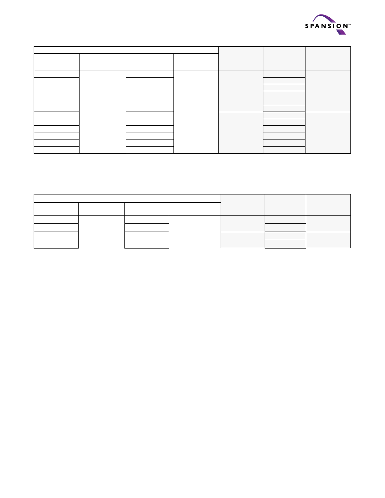
S71PL127J Valid Combinations
Base Ordering
Part Number
S71PL127JB0
S71PL127JB0 9U
S71PL127JC0 9B
S71PL127JC0 9Z pSRAM7 / 70
S71PL127JC0 9U
S71PL127JB0 9B
S71PL127JB0
S71PL127JB0 9U
S71PL127JC0 9B
S71PL127JC0 9Z
S71PL127JC0 9U
S71PL127JB0 9B
Notes:
1. Type 0 is standard. Specify other options as required.
2. BGA package marking omits leading “S” and packing type
designator from ordering part number.
Package &
Temperature
BAW
BFW
Package
Modifier/Model
Number
9Z
9Z
Packing Type
0, 2, 3 (Note 1)
0, 2, 3 (Note 1)
Valid Combinations list configuratio ns planned to be sup ported in volume for this device. Consult your local sales office to confirm availability of specific valid combinations and to check on newly released
combinations.
Speed Options
(ns)
65
65
(p)SRAM Type/
Access Time
(ns)
pSRAM7 / 70
pSRAM6 /70
pSRAM2 /70
pSRAM6 / 70
pSRAM2 / 70
pSRAM7 / 70
pSRAM6 / 70
pSRAM2 /70
pSRAM7 / 70
pSRAM6 / 70
pSRAM2 / 70
Valid Combinations
Package Marking
(Note 2)
(Note 2)
S71PL254J Valid Combinations
Base Ordering
Part Number
S71PL254JC0
S71PL254JC0 TZ
S71PL254JC0
S71PL254JC0 TZ
Notes:
1. Type 0 is standard. Specify other options as required.
2. BGA package marking omits leading “S” and packing type
designator from ordering part number.
Package &
Temperature
BAW
BFW
Model Number
TB
TB
Packing Type
0, 2, 3 (Note1)
0, 2, 3 (Note1)
Valid Combinations list configuratio ns planned to be sup ported in volume for this device. Consult your local sales office to confirm availability of specific valid combinations and to check on newly released
combinations.
Speed Options
(ns)
65
65
Valid Combinations
(p)SRAM
Type/Access
Time (ns)
pSRAM2 / 70
pSRAM7 / 70
pSRAM2 / 70
pSRAM7 / 70
Package
Marking
(Note 2)
(Note 2)
March 17, 2006 S71PL-J_00_B3 S71PL-J Based MCPs 13
Page 16
Advance Information
Physical Dimensions
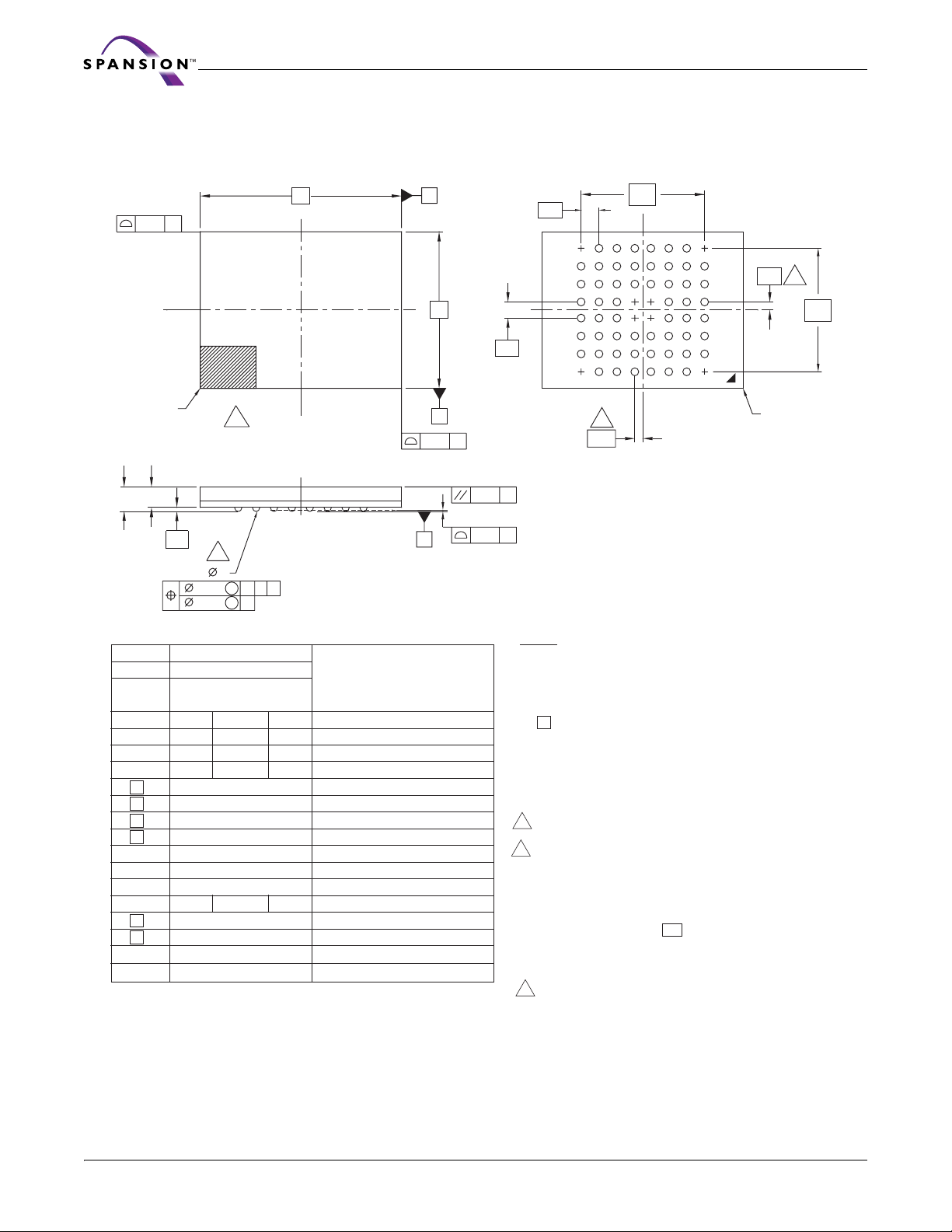
TLC056—56-ball Fine-Pitch Ball Grid Array (FBGA) 9 x 7mm Package
D
C
0.15
(2X)
PIN A1
CORNER
INDEX MARK
10
TOP VIEW
A2
A
A1
6
b
56X
0.15 MMCCAB
0.08
PACKAGE TLC 056
JEDEC N/A
D x E 9.00 mm x 7.00 mm
SYMBOL MIN NOM MAX NOTE
A --- --- 1.20 PROFILE
A1 0.20 --- --- BALL HEIGHT
A2 0.81 --- 0.97 BODY THICKNESS
D 9.00 BSC. BODY SIZE
E 7.00 BSC. BODY SIZE
D1 5.60 BSC. MATRIX FOOTPRINT
E1 5.60 BSC. MATRIX FOOTPRINT
MD 8 MATRIX SIZE D DIRECTION
ME 8 MATRIX SIZE E DIRECTION
n 56 BALL COUNT
φb 0.35 0.40 0.45 BALL DIAMETER
eE 0.80 BSC. BALL PITCH
eD 0.80 BSC BALL PITCH
SD / SE 0.40 BSC. SOLDER BALL PLACEMENT
PACKAGE
A1,A8,D4,D5,E4,E5,H1,H8 DEPOPULATED SOLDER BALLS
SIDE VIEW
C
A
0.15
(2X)
eD
D1
8
7
6
eE
5
4
3
2
1
DCEFGH
A
B
7
SD
E
B
C
SE
7
PIN A1
CORNER
E1
BOTTOM VIEW
0.20
C
C
0.08
NOTES:
1. DIMENSIONING AND TOLERANCING METHODS PER
ASME Y14.5M-1994.
2. ALL DIMENSIONS ARE IN MILLIMETERS.
3. BALL POSITION DESIGNATION PER JESD 95-1, SPP-010.
4. e REPRESENTS THE SOLDER BALL GRID PITCH.
5. SYMBOL "MD" IS THE BALL MATRIX SIZE IN THE "D"
DIRECTION.
SYMBOL "ME" IS THE BALL MATRIX SIZE IN THE
"E" DIRECTION.
n IS THE NUMBER OF POPULTED SOLDER BALL POSITIONS
FOR MATRIX SIZE MD X ME.
6 DIMENSION "b" IS MEASURED AT THE MAXIMUM BALL
DIAMETER IN A PLANE PARALLEL TO DATUM C.
7 SD AND SE ARE MEASURED WITH RESPECT TO DATUMS A
AND B AND DEFINE THE POSITION OF THE CENTER SOLDER
BALL IN THE OUTER ROW.
WHEN THERE IS AN ODD NUMBER OF SOLDER BALLS IN THE
OUTER ROW SD OR SE = 0.000.
WHEN THERE IS AN EVEN NUMBER OF SOLDER BALLS IN THE
OUTER ROW, SD OR SE = e/2
8. "+" INDICATES THE THEORETICAL CENTER OF DEPOPULATED
BALLS.
9. N/A
10 A1 CORNER TO BE IDENTIFIED BY CHAMFER, LASER OR INK
MARK, METALLIZED MARK INDENTATION OR OTHER MEANS.
3348 \ 16-038.22a
14 S71PL-J Based MCPs S71PL-J_00_B3 March 17, 2006
Page 17
Advance Information
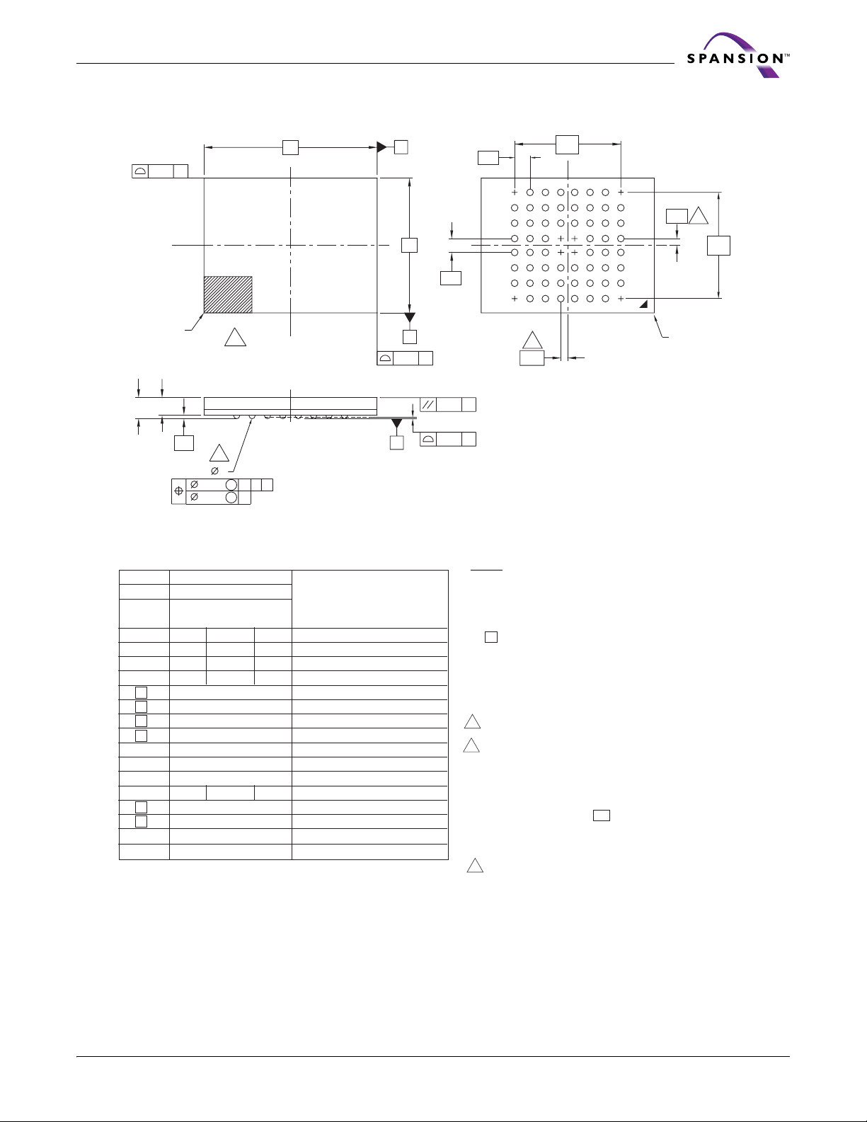
TSC056—56-ball Fine-Pitch Ball Grid Array (FBGA) 9 x 7mm Package
0.15
(2X)
PIN A1
CORNER
A
A2
C
INDEX MARK
A1
56X
0.15 MMCCAB
0.08
D1
DCEFGH
7
SD
BOTTOM VIEW
SE
7
E1
A
B
PIN A1
CORNER
C
A
0.15
(2X)
eD
8
7
6
eE
0.20
0.08
5
4
3
2
1
C
C
E
B
C
D
10
TOP VIEW
6
SIDE VIEW
b
PACKAGE TSC 056
JEDEC N/A
D x E 9.00 mm x 7.00 mm
SYMBOL MIN NOM MAX NOTE
A --- --- 1.20 PROFILE
A1 0.17 --- --- BALL HEIGHT
A2 0.81 --- 0.97 BODY THICKNESS
D 9.00 BSC. BODY SIZE
E 7.00 BSC. BODY SIZE
D1 5.60 BSC. MATRIX FOOTPRINT
E1 5.60 BSC. MATRIX FOOTPRINT
MD 8 MATRIX SIZE D DIRECTION
ME 8 MATRIX SIZE E DIRECTION
n 56 BALL COUNT
φb 0.35 0.40 0.45 BALL DIAMETER
eE 0.80 BSC. BALL PITCH
eD 0.80 BSC BALL PITCH
SD / SE 0.40 BSC. SOLDER BALL PLACEMENT
PACKAGE
A1,A8,D4,D5,E4,E5,H1,H8 DEPOPULATED SOLDER BALLS
NOTES:
1. DIMENSIONING AND TOLERANCING METHODS PER
ASME Y14.5M-1994.
2. ALL DIMENSIONS ARE IN MILLIMETERS.
3. BALL POSITION DESIGNATION PER JESD 95-1, SPP-010.
4. e REPRESENTS THE SOLDER BALL GRID PITCH.
5. SYMBOL "MD" IS THE BALL MATRIX SIZE IN THE "D"
DIRECTION.
SYMBOL "ME" IS THE BALL MATRIX SIZE IN THE
"E" DIRECTION.
n IS THE NUMBER OF POPULTED SOLDER BALL POSITIONS
FOR MATRIX SIZE MD X ME.
6 DIMENSION "b" IS MEASURED AT THE MAXIMUM BALL
DIAMETER IN A PLANE PARALLEL TO DATUM C.
7 SD AND SE ARE MEASURED WITH RESPECT TO DATUMS A
AND B AND DEFINE THE POSITION OF THE CENTER SOLDER
BALL IN THE OUTER ROW.
WHEN THERE IS AN ODD NUMBER OF SOLDER BALLS IN THE
OUTER ROW SD OR SE = 0.000.
WHEN THERE IS AN EVEN NUMBER OF SOLDER BALLS IN THE
OUTER ROW, SD OR SE = e/2
8. "+" INDICATES THE THEORETICAL CENTER OF DEPOPULATED
BALLS.
9. N/A
10 A1 CORNER TO BE IDENTIFIED BY CHAMFER, LASER OR INK
MARK, METALLIZED MARK INDENTATION OR OTHER MEANS.
3427 \ 16-038.22
March 17, 2006 S71PL-J_00_B3 S71PL-J Based MCPs 15
Page 18
Advance Information
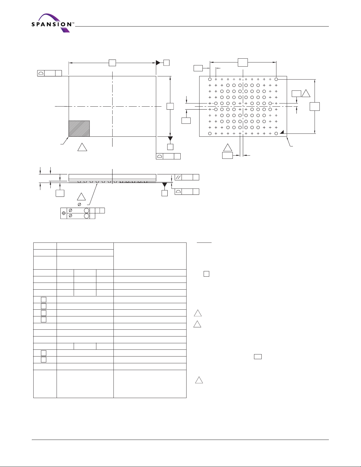
TLA064—64-ball Fine-Pitch Ball Grid Array (FBGA) 8 x 11.6mm Package
0.15
(2X)
PIN A1
CORNER
A2
A
C
A1
INDEX MARK
10
6
b
64X
0.15 M C A B
0.08 M C
D
TOP VIEW
SIDE VIEW
C
A
0.15
(2X)
eD
D1
10
9
8
7
eE
6
5
4
3
2
1
M
J
L
K
ABDCEFHG
7
SD
E
B
C
SE
7
PIN A1
CORNER
E1
BOTTOM VIEW
0.20
C
C
0.08
PACKAGE TLA 064
JEDEC N/A
D x E 11.60 mm x 8.00 mm
SYMBOL MIN NOM MAX NOTE
A --- --- 1.20 PROFILE
A1 0.17 --- --- BALL HEIGHT
A2 0.81 --- 0.97 BODY THICKNESS
D 11.60 BSC. BODY SIZE
E 8.00 BSC. BODY SIZE
D1 8.80 BSC. MATRIX FOOTPRINT
E1 7.20 BSC. MATRIX FOOTPRINT
MD 12 MATRIX SIZE D DIRECTION
ME 10 MATRIX SIZE E DIRECTION
n 64 BALL COUNT
φb 0.35 0.40 0.45 BALL DIAMETER
eE 0.80 BSC. BALL PITCH
eD 0.80 BSC BALL PITCH
SD / SE 0.40 BSC. SOLDER BALL PLACEMENT
C1,C2,C9,C10,D1,D10,E1,E10,
PACKAGE
A2,A3,A4,A5,A6,A7,A8,A9 DEPOPULATED SOLDER BALLS
B1,B2,B3,B4,B7,B8,B9,B10
F1,F5,F6,F10,G1,G5,G6,G10
H1,H10,J1,J10,K1,K2,K9,K10
L1,L2,L3,L4,L7,L8,L9,L10
M2,M3,M4,M5,M6,M7,M8,M9
NOTES:
1. DIMENSIONING AND TOLERANCING METHODS PER
ASME Y14.5M-1994.
2. ALL DIMENSIONS ARE IN MILLIMETERS.
3. BALL POSITION DESIGNATION PER JESD 95-1, SPP-010.
4. e REPRESENTS THE SOLDER BALL GRID PITCH.
5. SYMBOL "MD" IS THE BALL MATRIX SIZE IN THE "D"
DIRECTION.
SYMBOL "ME" IS THE BALL MATRIX SIZE IN THE
"E" DIRECTION.
n IS THE NUMBER OF POPULTED SOLDER BALL POSITIONS
FOR MATRIX SIZE MD X ME.
6 DIMENSION "b" IS MEASURED AT THE MAXIMUM BALL
DIAMETER IN A PLANE PARALLEL TO DATUM C.
7 SD AND SE ARE MEASURED WITH RESPECT TO DATUMS A
AND B AND DEFINE THE POSITION OF THE CENTER SOLDER
BALL IN THE OUTER ROW.
WHEN THERE IS AN ODD NUMBER OF SOLDER BALLS IN THE
OUTER ROW SD OR SE = 0.000.
WHEN THERE IS AN EVEN NUMBER OF SOLDER BALLS IN THE
OUTER ROW, SD OR SE = e/2
8. "+" INDICATES THE THEORETICAL CENTER OF DEPOPULATED
BALLS.
9. N/A
10 A1 CORNER TO BE IDENTIFIED BY CHAMFER, LASER OR INK
MARK, METALLIZED MARK INDENTATION OR OTHER MEANS.
3352 \ 16-038.22a
16 S71PL-J Based MCPs S71PL-J_00_B3 March 17, 2006
Page 19
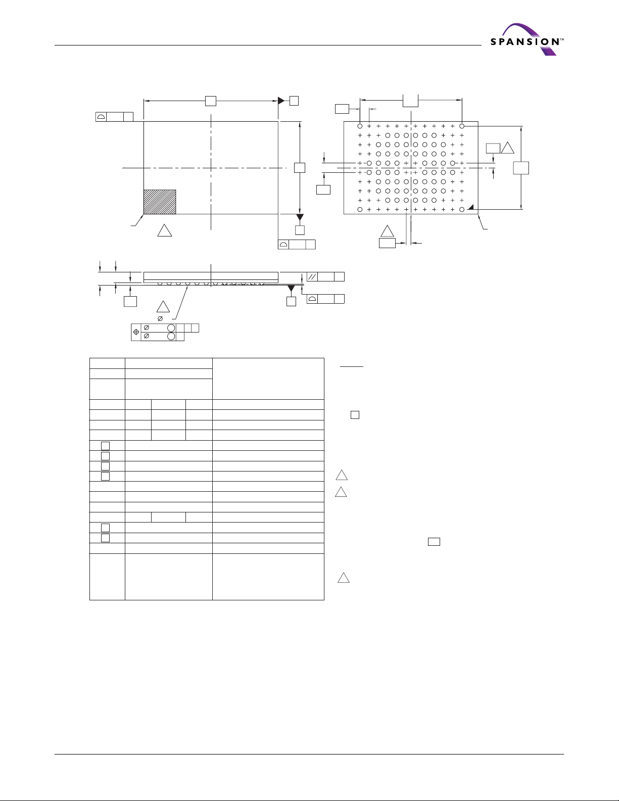
Advance Information
TSB064—64-ball Fine-Pitch Ball Grid Array (FBGA) 8 x 11.6 mm Package
D
C
0.15
(2X)
PIN A1
CORNER
INDEX MARK
10
TOP VIEW
A2
A
A1
PACKAGE TSB 064
JEDEC N/A
D x E 11.60 mm x 8.00 mm
SYMBOL MIN NOM MAX NOTE
A --- --- 1.20 PROFILE
A1 017 --- --- BALL HEIGHT
A2 0.81 --- 0.97 BODY THICKNESS
D 11.60 BSC. BODY SIZE
E 8.00 BSC. BODY SIZE
D1 8.80 BSC. MATRIX FOOTPRINT
E1 7.20 BSC. MATRIX FOOTPRINT
MD 12 MATRIX SIZE D DIRECTION
ME 10 MATRIX SIZE E DIRECTION
n 64 BALL COUNT
φb 0.35 0.40 0.45 BALL DIAMETER
eE 0.80 BSC. BALL PITCH
eD 0.80 BSC BALL PITCH
SD / SE 0.40 BSC. SOLDER BALL PLACEMENT
C1,C2,C9,C10,D1,D10,E1,E10
F1,F5,F6,F10,G1,G5,G6,G10
H1,H10,J1,J10,K1,K2,K9,K10
M2,M3,M4,M5,M6,M7,M8,M9
6
b
64X
0.15 M C A B
0.08 M C
PACKAGE
A2,A3,A4,A5,A6,A7,A8,A9 DEPOPULATED SOLDER BALLS
B1,B2,B3,B4,B7,B8,B9,B10
L1,L2,L3,L4,L7,L8,L9,L10
SIDE VIEW
C
A
0.15
(2X)
eD
D1
10
9
8
7
E
B
6
5
4
eE
3
2
1
JH
L
M
GFE
K
7
C
SD
ACDB
SE
7
PIN A1
CORNER
E1
BOTTOM VIEW
0.20
C
C
0.08
NOTES:
1. DIMENSIONING AND TOLERANCING METHODS PER
ASME Y14.5M-1994.
2. ALL DIMENSIONS ARE IN MILLIMETERS.
3. BALL POSITION DESIGNATION PER JESD 95-1, SPP-010.
4. e REPRESENTS THE SOLDER BALL GRID PITCH.
5. SYMBOL "MD" IS THE BALL MATRIX SIZE IN THE "D"
DIRECTION.
SYMBOL "ME" IS THE BALL MATRIX SIZE IN THE
"E" DIRECTION.
n IS THE NUMBER OF POPULTED SOLDER BALL POSITIONS
FOR MATRIX SIZE MD X ME.
6 DIMENSION "b" IS MEASURED AT THE MAXIMUM BALL
DIAMETER IN A PLANE PARALLEL TO DATUM C.
7 SD AND SE ARE MEASURED WITH RESPECT TO DATUMS A
AND B AND DEFINE THE POSITION OF THE CENTER SOLDER
BALL IN THE OUTER ROW.
WHEN THERE IS AN ODD NUMBER OF SOLDER BALLS IN THE
OUTER ROW SD OR SE = 0.000.
WHEN THERE IS AN EVEN NUMBER OF SOLDER BALLS IN THE
OUTER ROW, SD OR SE = e/2
8. "+" INDICATES THE THEORETICAL CENTER OF DEPOPULATED
BALLS.
9. N/A
10 A1 CORNER TO BE IDENTIFIED BY CHAMFER, LASER OR INK
MARK, METALLIZED MARK INDENTATION OR OTHER MEANS.
3351 \ 16-038.22a
March 17, 2006 S71PL-J_00_B3 S71PL-J Based MCPs 17
Page 20
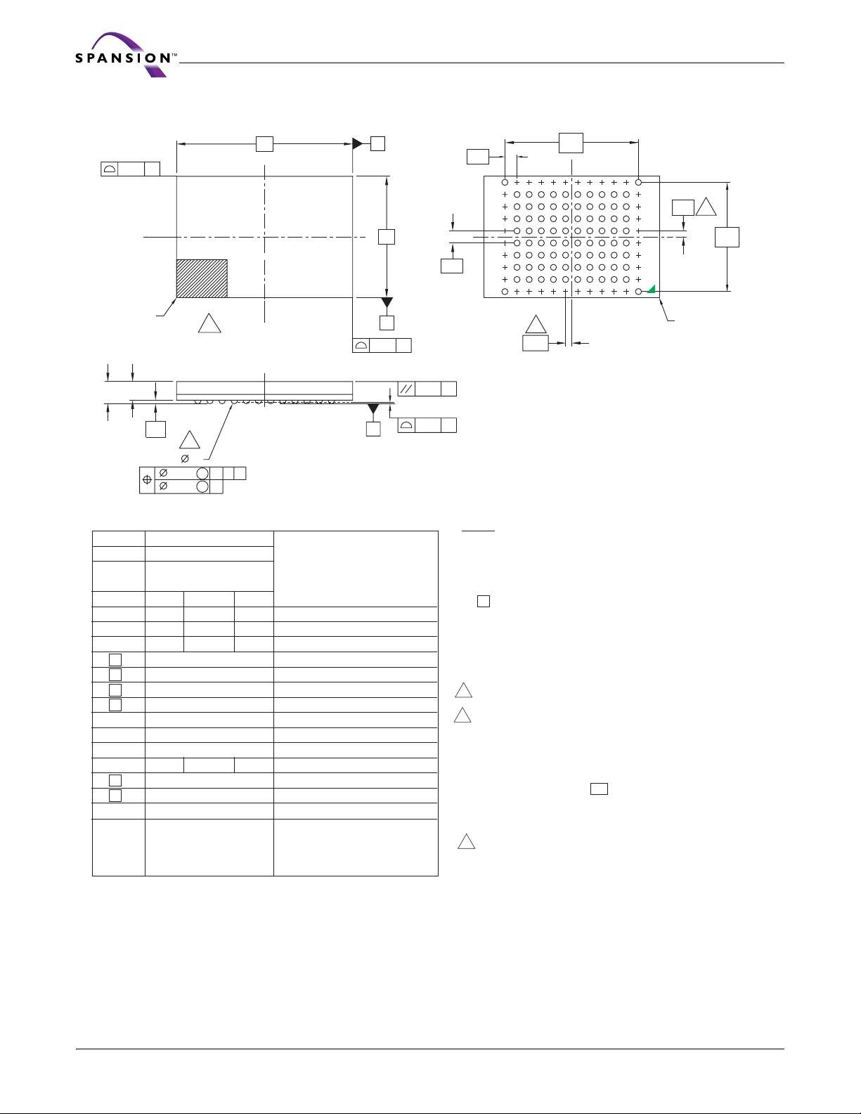
Advance Information
FTA084—84-ball Fine-Pitch Ball Grid Array (FBGA) 8 x 11.6mm Package
A
0.15
D
C
(2X)
PIN A1
CORNER
INDEX MARK
10
TOP VIEW
0.15
(2X)
A2
A
A1
6
b
84X
0.15 M C
0.08
PACKAGE FTA 084
JEDEC N/A
D x E 11.60 mm x 8.00 mm NOTE
SYMBOL MIN NOM MAX
A --- --- 1.40 PROFILE
A1 0.17 --- --- BALL HEIGHT
A2 1.02 --- 1.17 BODY THICKNESS
D 11.60 BSC. BODY SIZE
E 8.00 BSC. BODY SIZE
D1 8.80 BSC. MATRIX FOOTPRINT
E1 7.20 BSC. MATRIX FOOTPRINT
MD 12 MATRIX SIZE D DIRECTION
ME 10 MATRIX SIZE E DIRECTION
n 84 BALL COUNT
φb 0.35 0.40 0.45 BALL DIAMETER
eE 0.80 BSC. BALL PITCH
eD 0.80 BSC BALL PITCH
SD / SE 0.40 BSC. SOLDER BALL PLACEMENT
PACKAGE
A2,A3,A4,A5,A6,A7,A8,A9 DEPOPULATED SOLDER BALLS
B1,B10,C1,C10,D1,D10,E1,E10
F1,F10,G1,G10,H1,H10
J1,J10,K1,K10,L1,L10
M2,M3,M4,M5,M6,M7,M8,M9
SIDE VIEW
AB
MC
C
eD
D1
10
9
8
7
eE
6
5
4
3
2
1
ML
K
DCEFGHJ
B
7
SD
E
B
C
SE
7
E1
A
PIN A1
CORNER
BOTTOM VIEW
0.20
C
C
0.08
NOTES:
1. DIMENSIONING AND TOLERANCING METHODS PER
ASME Y14.5M-1994.
2. ALL DIMENSIONS ARE IN MILLIMETERS.
3. BALL POSITION DESIGNATION PER JESD 95-1, SPP-010.
4. e REPRESENTS THE SOLDER BALL GRID PITCH.
5. SYMBOL "MD" IS THE BALL MATRIX SIZE IN THE "D"
DIRECTION.
SYMBOL "ME" IS THE BALL MATRIX SIZE IN THE
"E" DIRECTION.
n IS THE NUMBER OF POPULTED SOLDER BALL POSITIONS
FOR MATRIX SIZE MD X ME.
6 DIMENSION "b" IS MEASURED AT THE MAXIMUM BALL
DIAMETER IN A PLANE PARALLEL TO DATUM C.
7 SD AND SE ARE MEASURED WITH RESPECT TO DATUMS A
AND B AND DEFINE THE POSITION OF THE CENTER SOLDER
BALL IN THE OUTER ROW.
WHEN THERE IS AN ODD NUMBER OF SOLDER BALLS IN THE
OUTER ROW SD OR SE = 0.000.
WHEN THERE IS AN EVEN NUMBER OF SOLDER BALLS IN THE
OUTER ROW, SD OR SE = e/2
8. "+" INDICATES THE THEORETICAL CENTER OF DEPOPULATED
BALLS.
9. N/A
10 A1 CORNER TO BE IDENTIFIED BY CHAMFER, LASER OR INK
MARK, METALLIZED MARK INDENTATION OR OTHER MEANS.
3388 \ 16-038.21a
18 S71PL-J Based MCPs S71PL-J_00_B3 March 17, 2006
Page 21

Advance Information
MCP Revision Summary
Revision A (May 3, 2004)
Initial release.
Revision A1 (May 6, 2004)
MCP Features
Corrected the high performance access times.
Connection Diagrams
Added reference points on all diagrams.
Ordering Information
Corrected package types.
Corrected the description of product family to Page Mode Flash memory.
pSRAM Type 1
Corrected the description of the 8Mb device to 512Kb Word x 16-bit.
pSRAM Type 6
Corrected the description of the 2Mb device to 128Kb Word x 16-bit.
Corrected the description of the 4Mb device to 256Kb Word x 16-bit.
Revision A2 (May 11, 2004)
General Description
Corrected the tables to reflect accurate device configurations.
Revision A3 (June 16, 2004)
Ordering Information
Corrected the Valid Combinations tables to reflect accurate device configurations.
SRAM
New section added.
Revision A4 (July 16, 2004)
Global Changes
Global Change of FASL to Spansion.
Global change to remove space between M and Mb callouts.
“32Mb Flash Memory” on page 3
Replaced “S71PL032J08-07” with “S71PL032J08-0B”.
Replaced “S71PL032JA0” with “S71PL032JA0-07”.
Added row with the following content: S71PL032JA0-08; 65; 16Mb pSRAM; 70;
pSRAM3; TLC056.
“64Mb Flash Memory” on page 3
Replaced “
Replaced “
Deleted “S71PL064J80-05” row.
Replaced “
S71PL064J08-0K” with “S71PL064J08-0B”.
S71PL064J08-0P” with “S71PL064J08-0U”.
S71PL064JA0-07” with “S71PL064JA0-0K”.
March 17, 2006 S71PL-J_00_B3 S71PL-J Based MCPs 19
Page 22

Advance Information
Replaced “
Added row with the following content:
1; TLC056.
S71PL064JA0-0Z” with
S71PL064JB0-07; 65; 32M pSRAM; 70; Psram
“32Mb Flash Memory” on page 3
Replaced “
S71PL032JA0-08” with “S71PL032JA0-0F”.
“64Mb Flash Memory” on page 3
Replaced “
S71PL032JA0-07” with “S71PL032JA0-0K”.
“128Mb Flash Memory” on page 4
Added row with the following content: S71PL127JB0-9; 65; 32M pSRAM; 70;
pSRAM; TLA064.
Replaced “S71PL127JB0-97” with “
Added row with the following content: S71PL127JC0-97; 65; 64M pSRAM; 70;
pSRAM1; TLA064.
Replaced “
In the S71Pl254JB0-TB row changed pSRAM type from “
S71PL127JC0-9P” with “S71PL127JC0-9Z”.
S71PL127JB0-9Z”.
“256Mb Flash Memory (2xS29PL127J)” on page 4
Added row with the following content: S71PL254JB0-TB; 65; 32M pSRAM; 70;
pSRAM3; FTA084.
Added row with the following content:
pSRAM2; FTA084.
pSRAM3” to “pSRAM2”.
S71PL254JC0-TB; 65; 64M pSRAM; 70;
“Connection Diagram (S71PL127J)” on page 12
Updated pins D8, D9, and L5.
Added notes 2 and 3 to drawing.
“Connection Diagram (S71PL254J)” on page 13
Updated pins D8 and D9.
Added Note 2 to drawing.
“S71PL032J Valid Combinations” on page 16
Changed S71PL032J08 (p)SRAM Type Access Time (ns) from “SRAM1” to
“SRAM2” (4 changes made in table).
Changed S71PL032JA0 (p)SRAM Type Access Time (ns) from “SRAM3 / 70” to
pSRAM3 /70”.
Deleted all cells with the following collaborated text: “BAW,BFW, BAI. BFI”.
Merged previous place holder with cell above.
“S71PL064J Valid Combinations” on page 17
In (p)SRAM Type/Access Time (ns) changed all instances of “ste t” to “pSRAM1/
70”.
In Package Modifier/Model Number changed all instances of “stet” to “07”.
Added row to BAW Package and Temperature sections with the following content:
S71PL064JB0; 07; 65 (previously inclusive); pSRAM1/70.
“S71PL127J Valid Combinations” on page 18
Changed the S71PL127JA0 Packag e Modifier/M odel Number from “9Z” to “9P” (4
instances).
20 S71PL-J Based MCPs S71PL-J_00_B3 March 17, 2006
Page 23

Advance Information
Added 4 rows with the following content: S71PL127JC0; 97; pSRAM1/70 .
“S71PL254J Valid Combinations” on page 20
Added 4 rows with the following content: S71PL254JC0; TB; pSRAM2 /7 0.
Added 4 rows with the following content: S71PL254JB0; TB; pSRAM2/70.
“S71PL-J based MCPs” on page 1
Added 254M to Megabit indicator.
Added 16 to CMOS indicator.
Revision A5 (September 14, 2004)
Product Selector Guide
Updated the 128Mb Flash Memory table.
Valid Combinations Table
Updated the S71PL127J Valid Combinations table.
Revision A6 (November 22, 2004)
Product Selector Guide
Updated the 32Mb and 64Mb tables.
Valid Combinations Tables
Updated the 32Mb and 64Mb combinations.
Physical Dimensions
Added the TSB064 package.
Revision A7 (February 8, 2005)
pSRAM Type 7
Updated all information in this section.
Revision A8 (April 6, 2005)
S29PL-J Flash
Updated all information in this section.
Revision A9 (May 12, 2005)
S71PL-J MCP
Added the S71PL064J0A option to cover the inclusion of the 16M SRAM
pSRAM Type 2
Added the latest revision for the pSRAM Type 2
SRAM Type 2
Added this module to the S71PL-J MCP
Revision A10 (June 22, 2005)
S71PL-J MCP
Removed 127/16 and 254/32 pSRAM and updated OPN for 64/16SRAM
Revision A11 (July 29, 2005)
pSRAM Type 7
Updated module
March 17, 2006 S71PL-J_00_B3 S71PL-J Based MCPs 21
Page 24

Advance Information
Revision B0 (September 29, 2005)
S29PL-J
Updated module
SRAM Type 1
Updated module
Revision B1 (October 25, 2005)
pSRAM Module Type 5
Added module
Revision B2 (January 25, 2006)
Added notices for devices not recommended for new designs
Modified the Product Selection Guide
Modified the S71PL032J, S71PL064J, S71PL127JValid Combinations tables
Revision B3 (March 17, 2006)
Modified the stucture of the document. Related data sheets are referenced rather
than be embedded. Added data sheet reference table to that effect.
Added the SRAM Type 4 option
Added the 8Mb pSRAM Type 3 option
Colophon
The products described in this document are designed, developed and manufactured as contemplated for general use, including without limitation, ordinary
industrial use, general office use, personal use, and household use, but are not designed, developed and manufactured as contemplated (1) for any use that
includes fatal risks or dangers that, unless extremely high safety is secured, could have a serious effect to the public, and could lead directly to death, personal
injury, severe physical damage or other loss (i.e., nuclear reaction control in nuclear facility, aircraft flight control, air traffic control, mass transport control,
medical life support system, missile launch control in weapon system), or (2) for any use where chance of failure is intolerable (i.e., submersible repeater and
artificial satellite). Please note that Spansion will not be liable to you and/or any third party for any claims or damages arising in connection with abovementioned uses of the products. Any semiconductor devices have an inherent chance of failure. You must protect against injury, damage or loss from such
failures by incorporating safety design measures into your facility and equipment such as redundancy, fire protection, and prevention of over-current levels
and other abnormal operating conditions. If any products described in this document represent goods or technologies subject to certain restrictions on export under the Foreign Exchange and Foreign Trade Law of Japan, the US Export Administration Regulations or the applicable laws of any other country, the
prior authorization by the respective government entity will be required for export of those products.
Trademarks and Notice
The contents of this document are subject to change without notice. This document may contain information on a Spansion LLC product under development
by Spansion LLC. Spansion LLC reserves the right to change or discontinue work on any product without notice. The information in this document is provided
as is without warranty o r guaran tee of any kind as to its accuracy, completeness, operability, fitness for particular purpose, merchantability, non-infringement
of third-party rights, or any other warranty, express, implied, or statutory. Spansion LLC assumes no liability for any damages of any kind arising out of the
use of the information in this document.
Copyright ©2004 – 2006 Spansion LLC. All Rights Reserved. Spansion, the Spansion logo, MirrorBit, ORNAND, and combinations thereof are trademarks
of Spansion LLC. Other names are for informational purposes only and may be trademarks of their respective owners.
22 S71PL-J Based MCPs S71PL-J_00_B3 March 17, 2006
 Loading...