

Page 1
A/D, D/C Converters for Image Signal Processing
MN6577F, MN6577H
Low Power 10-Bit 3-Volt CMOS A/D Converters for Image Processing
Overview
The MN6577F and MN6577H are high-speed 10-bit
CMOS analog-to-digital converters for image processing applications.
They use a half flash structure based on chopper comparators to achieve both high speed and low power consumption, and operate on a single 3 volt power supply.
Features
Maximum conversion rate: 15 MSPS (min.)
Linearity error: ±1.3 LSB (typ.)
Differential linearity error: ±0.5 LSB (typ.)
Power supply voltage: 3.0 V
Power consumption: 40 mW (typ.) (f
=15 MHz)
CLK
Applications
Digital television
Digital video equipment
Digital image processing equipment
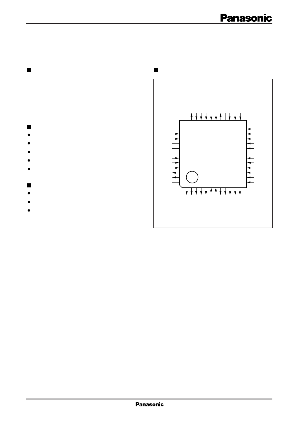
Pin Assignment
MN6577F TQFP048-P-0707
MN6577H QFH048-P-0707
RBSVRBVR3VR2VR1VRTVRTS
N.C.
V
3635343332313029282726
N.C.
AV
N.C.
N.C.
N.C.
AV
DV
DV
LINDF
OVF
N.C.
37
38
DD
39
V
IN
40
41
42
43
SS
44
SS
45
DD
46
47
48
1234567891011
D0D1D2D3D4
SS
D5D6D7D8D9
DDL
DV
DV
(TOP VIEW)
N.C.
AVSSAVDDAV
DD
25
24
POWD
23
NOE
22
CLK
21
MINV
20
LINV
19
N.C.
18
DV
17
16
15
14
13
12
DD
DV
SS
DV
SS
DV
DD
TEST1
TEST2
1
Page 2
MN6577F, MN6577H A/D, D/C Converters for Image Signal Processing
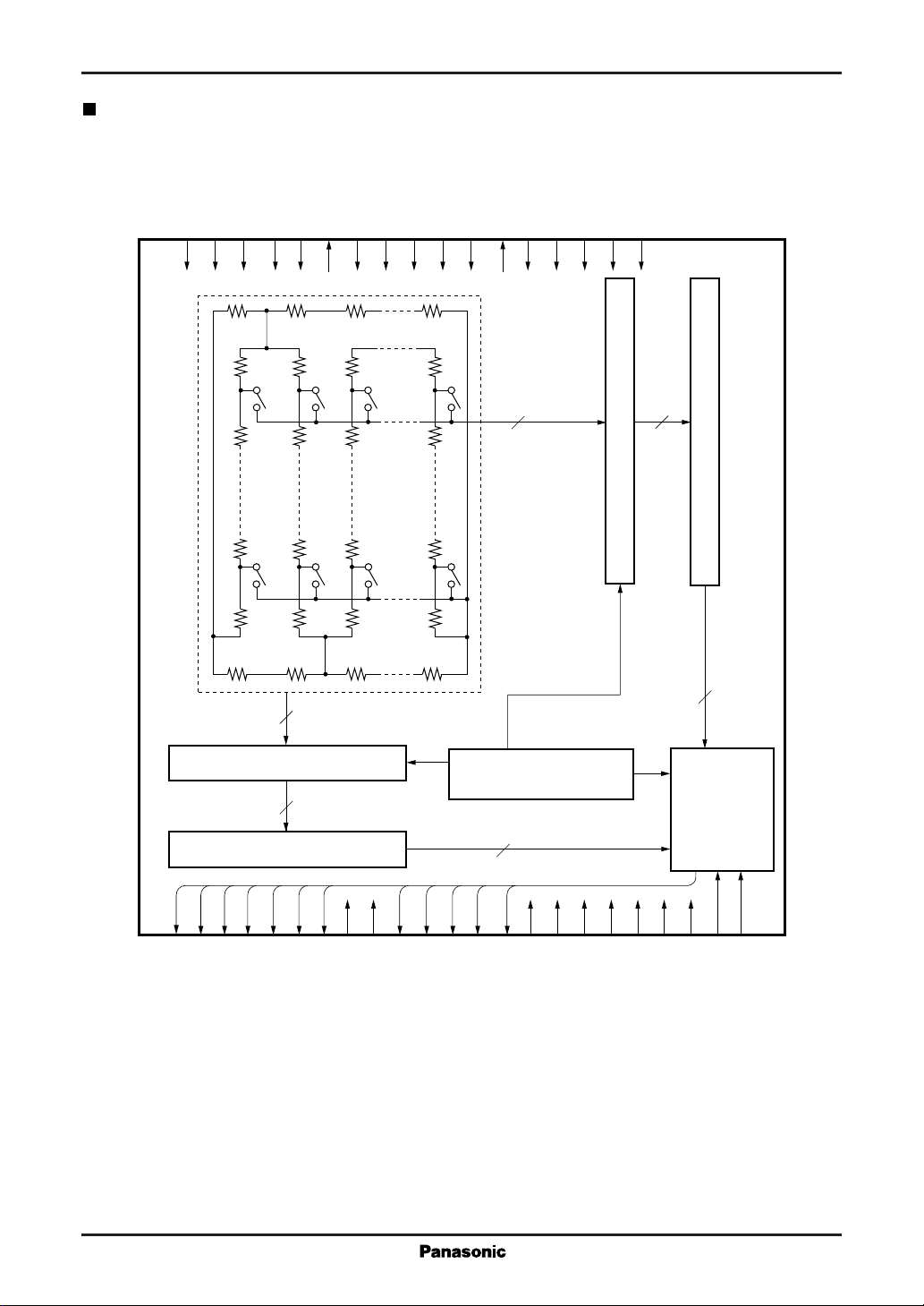
Block Diagram
Pins 19, 28, 36, 37, 40, 41, 42,
and 48 are no connention pins.
( )
DVDDDV
45
44
SS
SS
AV
43
DD
38
AV
35
V
RBS
IN
V
39
34
R3
RB
V
V
33
32
R1
R2
V
V
31
30
RTS
RT
V
V
29
DD
AV
AVSSAVDDLINV
27
26
25
MINV
21
29
Lower comparator (5 bits)
20
57
Lower encoder (5 bits)
5
31
Upper comparator (5 bits)
31
Clock generator
Error
correction
and
46
UNDF
47
1
OVF
(LSB)
D0
Encoder (5 bits)
2
3
4
5
D1
D2
D3
D4
5
6
7
8
9
10
11
12
13
14
15
16
17
SS
DV
DDL
DV
D5
D6D7D8
D9
TEST2
TEST1
DD
DV
DVSSDV
SS
18
DD
DV
data latch
22
23
CLK
NOE
24
POWD
2
Page 3
A/D, D/C Converters for Image Signal Processing MN6577F, MN6577H
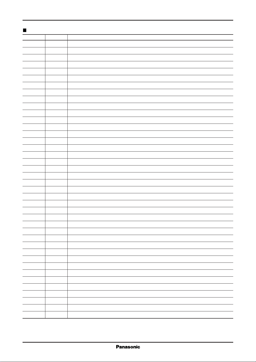
Pin Descriptions
Pin No. Symbol Function Description
1 D0 Digital code output (LSB)
2 D1 Digital code output
3 D2 Digital code output
4 D3 Digital code output
5 D4 Digital code output
6DVSSGround for digital circuits
7DVDDPower supply for digital circuits
8 D5 Digital code output
9 D6 Digital code output
10 D7 Digital code output
11 D8 Digital code output
12 D9 Digital code output (MSB)
13 TEST2 Test mode selection pin
14 TEST1 Test mode selection pin
15 DV
16 DV
17 DV
18 DV
DD
SS
SS
DD
19 N.C. No connection
20 LINV Output inversion pin
21 MINV Output inversion pin
22 CLK Sampling clock
23 NOE Digital output enable pin
24 POWD Power down mode selection pin
25 AV
26 AV
27 AV
DD
DD
SS
28 N.C. No connection
29 V
30 V
31 V
32 V
33 V
34 V
35 V
RTS
RT
R1
R2
R3
RB
RBS
36 N.C. No connection
37 N.C. No connection
38 AV
39 V
DD
IN
40 N.C. No connection
Power supply for digital circuits
Ground for digital circuits
Ground for digital circuits
Power supply for digital circuits
Power supply for analog circuits
Power supply for analog circuits
Ground for analog circuits
Reference voltage power supply (TOP)
Reference voltage input (TOP)
Intermediate reference voltage
Intermediate reference voltage
Intermediate reference voltage
Reference voltage input (BOTTOM)
Reference voltage power supply (BOTTOM)
Power supply for analog circuits
Analog signal input
3
Page 4

MN6577F, MN6577H A/D, D/C Converters for Image Signal Processing
Pin Description (continued)
Pin No. Symbol Function Description
41 N.C. No connection
42 N.C. No connection
43 AV
44 DV
45 DV
SS
SS
DD
46 UNDF Underflow output
47 OVF Overflow output
48 N.C. No connection
Absolute Maximum Ratings Ta=25˚C
Parameter Symbol Rating Unit
Power supply voltage V
Input voltage V
Output voltage V
Operating ambient temperature T
Storage temperature T
Recommended Operating Conditions
Parameter Symbol min typ max Unit
Power supply voltage V
Digital input "H" level V
voltage "L" level V
Reference "H" level V
voltage "L" level V
Clock "H" level pulse width t
Analog input voltage V
Electrical Characteristics V
Parameter Symbol Conditions min typ max Unit
Power consumption P
Resolution RES 10 bit
Linearity error E
Differential linearity error E
Maximum conversion rate F
Clock frequency f
Analog input dynamic range D
Output "H" level I
current "L" level I
Output delay time t
Analog input capacitance C
Sampling delay t
Ground for analog circuits
Ground for digital circuits
Power supply for digital circuits
"L" level pulse width t
=AVDD=DVDD=3.0V , AVSS=DVSS=0V, Ta=25˚C
DD
FC=15MSPS
C
(not including reference current)
f
L
CLK
VRT=3.0V
D
VBB=1.0V
C(max.)
CLK
R
VOH=V
OH
VOL=0.4V 1.5 mA
OL
CL=20pF 10 20 40 ns
d
I
sd
– 0.3 to +7.0 V
– 0.3 to V
– 0.3 to V
+0.3 V
DD
+0.3 V
DD
–20 to +70 ˚C
–55 to +125 ˚C
DD
0.8 V
DD
1.0 V
V
DD
V
V
V
DD
WH
WL
AIN
RB
DD
I
O
opr
stg
V
=AVDD=DVDD=3.0V, VSS=AVSS=DVSS=0V, Ta=25˚C
DD
2.85 3.00 3.30 V
IH
IL
RT
2.4 V
V
SS
2.0 V
V
SS
30 ns
30 ns
V
SS
39 72 mW
=15MSPS ±1.3 ±2.5 LSB
±0.5 ±1.0 LSB
15 MSPS
1 15 MHz
2V
– 0.8V –1.5 mA
DD
RT
– V
RB
V
18 pF
7ns
4
Page 5

A/D, D/C Converters for Image Signal Processing MN6577F, MN6577H
Timing Chart
The chip samples the analog input at the falling edge of the clock signal and provides the corresponding digital
output 2.5 clock cycles later at the rising edge of the clock signal.
t
WHtWL
Clock
Analog input
Data output
t
sd
N
(7ns)
N+1
N+2
N–3 N–2 N–1 N+1N
(20ns)
t
d
Note: The circles indicate analog signal sampling points.
N+3
N+4
5
Page 6

MN6577F, MN6577H A/D, D/C Converters for Image Signal Processing
Package Dimensions (Unit:mm)
MN6577F TQFP048-P-0707
9.00±0.20
7.00±0.10
2536
37
48
(0.75)
0.10
0.50
121
+0.10
-
0.05
0.20
SEATING PLANE
24
13
(0.75)
(1.00)
1.20max.
0.10±0.10
7.00±0.10
0.05
-
+0.10
0.125
9.00±0.20
(1.00)
0 to 10°
0.50±0.10
6
Page 7

A/D, D/C Converters for Image Signal Processing MN6577F, MN6577H
Package Dimensions (Unit:mm)(continued)
MN6577H QFH048-P-0707
9.0±0.2
±0.2
7.0
36 25
37
48
(0.75)
24
(0.75)
7.0±0.2
9.0±0.2
13
1
0.5
12
0.2±0.1
(1.0)
±0.20.1±0.1
2.5
0.1
0.05
-
+0.10
2.9 max.
0.15
0.5±0.2
0 to 10°
SEATING PLANE
7
Page 8

 Loading...