

Page 1
ESS Technology, Inc. SAM0076-051701 1
ES3207
Video CD/DVD Companion Chip
Product Brief
DESCRIPTION
The ES3207 Video CD/DVD Companion Chip provides an
optimal system design fo r a Video CD player or a DVD
player.
The ES3207, which is an enhanced version of the pincompatible ES3205, integrates most of the required
analog discrete components into a simple, cost-effective
solution and interfaces directly to the ES3210 (Video CD)
or ES3308 (DVD). No glue logic or external microcontroller
is required.
The ES3207 features include a high-quality NTSC/PAL
Digital Video Encoder (DVE), echo, echo reverb,
3DSound, surround sound, vid eo and aud io DACs , and a
PLL clock synthesiz er. There are three 9-bit video DACs
(one for composite video output and two for S-video
outputs) and two 16-bit sigma-delta audio DACs for
interfacing with current sound systems.
The DVE generates composite and S-video analog
signals. Color Space Conve rsions (CSC) are prov ided to
match the input data to the requir ed output format, then
the data is filtered to meet the selected video standards. In
addition, the ES3207 i s equipped with a remote control
interface for power on/off, microphone ports, auxiliary
ports, and an interface for accessing internal registers.
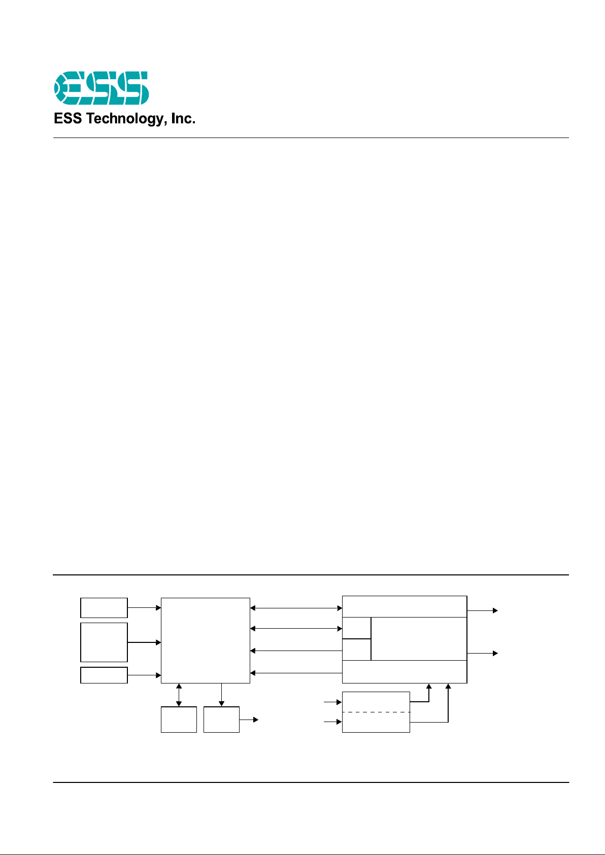
Figure 1 shows a block dia gram of a typical stand-alone
system using the ES3210 Video CD Processor Chip or the
ES3308 MPEG2 Audio/Video Decoder Chip and an
ES3207 Video CD Companion Chip.
FEATURES
• Multi-standard TV enco de r:
– CCIR601 non-square operation
– NTSC/PAL formats
– Master video mode
– 8-bit interface for YCrCb (4:2:2) input format
– Simultaneous composite and S-video output
– Interlaced operation
• Audio DACs:
– Two 16-bit sigma-delta DACs
– Accepts I
2
S format data
– Programmable functions
• 3DSound and surround sound
• Remote control inte rface f or pow er on/ of f
• Digitally controlled e cho wi th up t o 168 ms delay
• Vocal reverb for theater acoustical effects
• Dual microphone in put
• Clock synthesizer (PLL):
– Based on 27 MHz crystal input
– Generates required clocks for video encoder, audio
DAC, echo and surround sound, and video
processor
• Device Serial Communication (DSC) port for com mand
issued/register access
• Power management
• 100-Pin PQFP
• Single 5 V power supp ly
Figure 1 ES3207 Video CD Companion Chip System Block Diagram
ES3207
DRAM
Remote
VFD
VFD
Driver
Panel
Receiver
ES3210
CD-ROM
Audio DAC
3D/Echo/Surround
PLL
NTSC/PAL Video
DSC
ROM
Television
Speakers
(Video CD)
or
ES3308
(DVD)
or
DVD-ROM
Drive
Preamp
Volum e Contro l
Preamp
Volum e Contro l
Mic 1
Mic 2
Page 2
2 SAM0076-051701 ESS Technology, Inc.
ES3207 VIDEO CD CC PRODUCT BRIEF
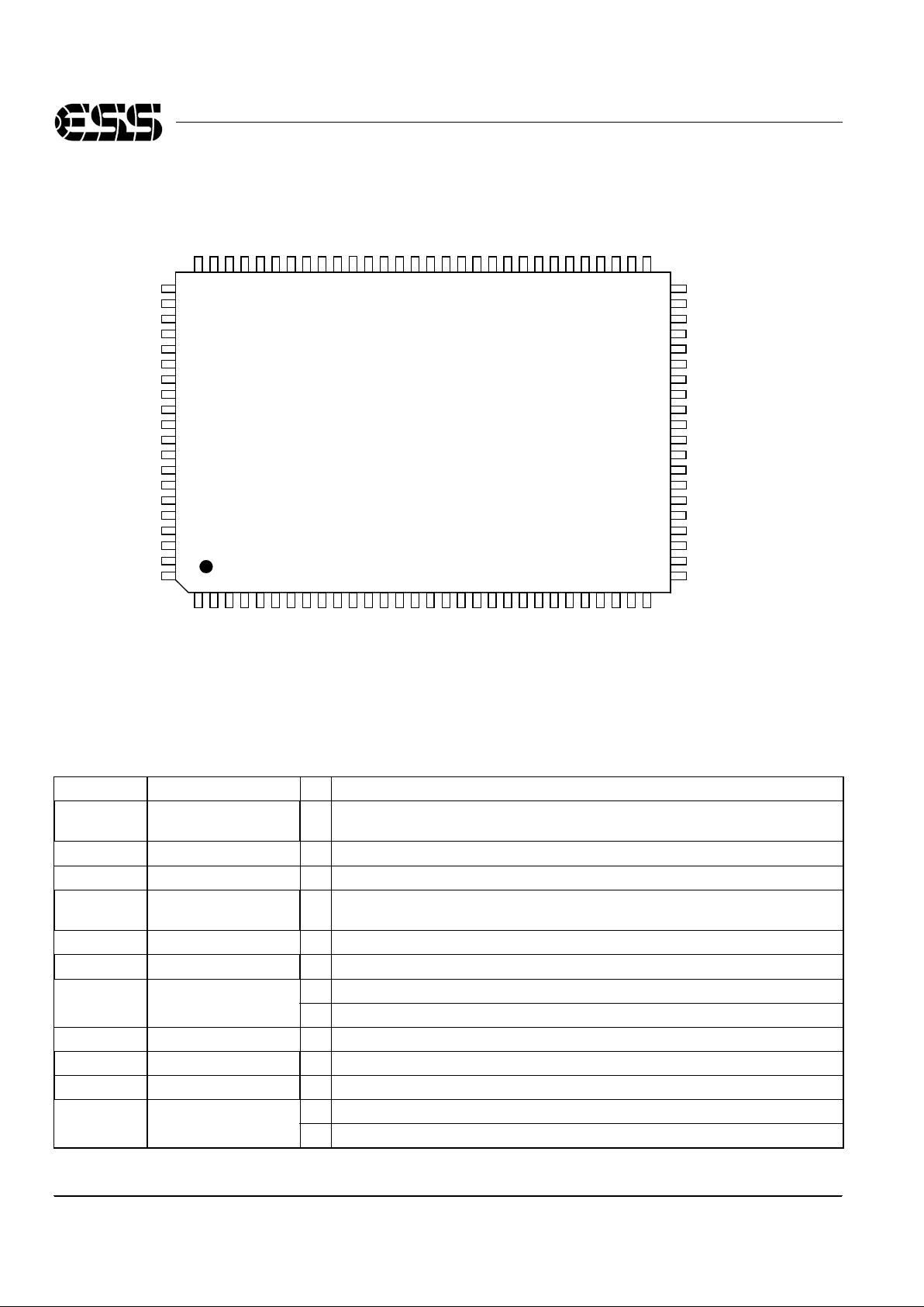
PINOUT
PINOUT
PIN DESCRIPTION
Name Number I/O Definition
VSS 1:2,25:26,29:31,72,75,
77,91,100
I Ground.
VCC 3:5,16,32,66,73,78,90 I Voltage supply, 5 V.
DSC_C 6 I Clock for programming to access internal registers.
AUX[15:0] 40:38,36:34,20,18,14,
67:70,11,9,7
I/O Auxiliary control pins.
DSC_D[7:0] 81,83,85,93,95,97,99,8 I/O Data for programming to access internal registers.
DSC_S 10 I Strobe for programming to access internal registers.
DCLK
12
O Dual-purpose pin. DCLK is the MPEG decoder clock.
EXT_CLK I EXT_CLK is the external clock. EXT_CLK is an input during bypass PLL mode.
RST# 13 I Video reset (active-low).
MUTE 15 O Audio mute.
MCLK 17 I Audio master clock.
TWS
19
I Dual-purpose pin. TWS is the transmit audio frame sync.
SPLL_OUT O SPLL_OUT is the select PLL output.
1
VSSA
MIC1
MIC2
AOL
AOR
VCCA
VCCA
VREFP
VREFM
VSSA
AUX15
AUX14
AUX13
RBCK / SER_IN
AUX12
AUX11
AUX10
RSD / SEL_PL L0
VCC
VSS
DSC_D7
HSYNC#
DSC_D6
VSYNC#
DSC_D5
YUV7
YUV6
YUV5
YUV4
VCC
VSS
YUV3
DSC_D4
YUV2
DSC_D3
YUV1
DSC_D2
YUV0
DSC_D1
VSS
TSD
AUX9
TWS / SPLL_OUT
AUX8
MCLK
VCC
MUTE
AUX7
RST#
DCLK / EXT_CLK
AUX2
DSC_S
AUX1
DSC_D0
AUX0
DSC_C
VCC
VCC
VSS
VSS
VSS
VSS
VCC
NC
NC
VSS
VSS
RSTOUT#
RWS / SEL_PLL1
TBCK
YDAC
VSSA
VSSA
VDAC
NC
VCC
AUX6
AUX5
AUX4
AUX3
XOUT
VSS
VCC
XIN
VSS
NC
VSS
VCC
PCLK
PCLK2X
VSSA
VREF
VCM
RSET
COMP
VSSA
VSSA
CDAC
VCCA
VCCA
31
30
51
50
80
81
100
234567891011121314151617181920212223242526272829
49
48
47
46
45
44
43
42
41
40
39
38
37
36
35
34
33
32
79 78 77 76 75 74 73 72 71 70 69 68 67 66 65 64 63 62 61 60 59 58 57 56 55 54 53 52
82
83
84
85
86
87
88
89
90
91
92
93
94
95
96
97
98
99
ES3207
Page 3

ESS Technology, Inc. SAM0076-051701 3
ES3207 VIDEO CD CC PRODUCT BRIEF
PIN DESCRIPTION
TSD 21 I Transmit audio data input.
TBCK 22 I Transmit audio bit clock.
RWS 23 O Dual-purpose pin. RWS is the receive audio frame sync.
SEL_PLL1 I Pins SEL_PLL[1:0] select the PLL clock frequency for the DCLK output.
RSTOUT# 24 O Reset output (active-low).
NC 27:28,65:76 No connect. Do not connect to these pins.
RSD
33
O Dual-purpose pin. RSD is the receiv e aud io dat a input.
SEL_PLL0
I SEL_PLL0 along with SEL_PLL1 select the PLL clock frequency for the DCLK out-
put. See the table for pin number 23.
RBCK
37
O Dual-purpose pin. RBCK is the recei ve aud io bit cloc k.
SER_IN
I SER_IN is the serial input DSC mode.
0 = Parallel DSC mode.
1 = Serial DSC mode.
VSSA 41,50:51,56:57,62:63 I Analog ground.
VREFM 42 I DAC and ADC minimum re fer ence. Bypa ss t o VC MR wi th 10 µF in parallel with 0.1 µF.
VREFP 43 I DAC and ADC maximum reference. Bypass to VCMR with 10 µF in parallel with 0.1 µF.
VCCA 44:45,59:60 I Analog VCC, 5 V.
AOR 46 O Right channel output.
AOL 47 O Left channel output.
MIC2 48 I Microphone input 2.
MIC1 49 I Microphone input 1.
VREF 52 I Internal resistor divider generates Common Mode Reference (CMR) voltage.
Bypass to analog ground with 0.1 µF.
VCM 53 I ADC Common Mode Referenc e (CMR) b uf fer o utput. CM R is a pproxima tely 2 .25 V.
Bypass to analog ground with 47 µF electrolytic in parallel with 0.1 µF.
RSET 54 I Full scale DAC current adjustment.
COMP 55 I Compensation pin.
CDAC 58 O Modulated chrominance output.
YDAC 61 O Y luminance data bus for sc reen video po rt.
VDAC 64 O Composite video output.
XOUT 71 O Crystal output.
XIN 74 I 27 MHz crystal input.
PCLK 79 I/O 13.5 MHz pixel clock.
PCLK2X 80 I/O 27 MHz (2 t im es p ix e l c lock).
HSYNC# 82 O Horizontal sy nc (active-l ow ).
VSYNC# 84 O Vertical sync (active-low ).
YUV[7:0] 86:89,92,94,96,98 I YUV data bus for screen video port.
Name Number I/O Definition
SEL_PLL1 SEL_PLL0 DCLK
0 0 Bypass PLL (input mode)
0 1 27 MHz (output mode)
1 0 32.4 MHz (output mode)
1 1 40.5 MHz (output mode)
Page 4

4 © 1997 ESS Technology, Inc. All rights reserved. SAM0076-051701
ES3207 VIDEO CD CC PRODUCT BRIEF
MECHANICAL DIMENSIONS
No part of this publication may be reproduced, stored in a
retrieval system, transmitted, or translated in any form or
by any means, electronic, mechanical, ma nual, opti cal, or
otherwise, without the prior written permission of ESS
Technology, Inc.
ESS Technology, Inc. makes no representations or
warranties regarding the content of this document.
All specifications are subject to change without prior
notice.
ESS Technology, Inc. assumes no responsibility for any
errors contained herein.
(P) U.S. Patent 4,214,125 and others, other patents
pending.
VideoDrive® is a registered trademark of ESS Technology,
Inc.
MPEG is the Moving Picture Experts Group of the ISO/IEC.
All other trademarks are owned by their respective
holders and are used for identification purposes only.
MECHANICAL DIMENSIONS
Symbol Description
Millimeters
Min Nom Max
D Lead to lead, X-axis 23.65 23.90 24.15
D1 Package’s outside, X-axis 19.90 20.00 20.10
E Lead to lead, Y-axis 17.65 17.90 18.15
E1 Package’s outside, Y-axis 13.90 14.00 14.10
A1 Board standoff 0.10 0.25 0.36
A2 Package thickness 2.57 2.71 2.87
bLead width0.20 0.30 0.40
e Lead pitch -0.65-
e1 Lead gap 0.24 - -
L Foot length 0.65 0.80 0.95
L1 Lead length 1.88 1.95 2.02
- Foot angle 0° -7°
- Coplanarity - - 0.102
- Leads in X-axis -30-
- Leads in Y-axis -20-
- Total leads -100-
- Package type -PQFP-
E1
A2 A1
L
E
D1
b
D
ES3207
e
1
e1
L1
100-Pin PQFP
 Loading...