

Page 1
ES2839/ES2840
V.90/V.92 PCI HSP Modem Solution
ESS Technology, Inc.
DESCRIPTION
The ES2839/ES2840 is a high-performance, two-chip, hostbased modem solution that delivers high connectivity and
throughput, using a solid-state DAA instead of a traditional
transformer DAA. The chipset consists of the ES2839 TeleDrive
modem chip and the ES2840, its accompanying high-voltage,
solid-state DAA device. Together, the ES2839 and ES2840
devices comprise a very low-cost modem solution for add-in
cards, desktops, and notebooks.
The ES2839 modem is capable of send/receive data and fax,
supports telephone answering machine (TAM), and is capable of
data/fax/voice call discrimination. With its built-in ACPI and
wake-on-ring support, the ES2839, plus the ES2840,
D3
cold
forms an ideal modem solution for notebooks and batteryoperated devices.
The ES2839 includes a PCI bus interface, codec, and lowvoltage, solid-state DAA. It also includes ADC and DAC
conversions of modem/voice signal data and provides the
interface and control logic needed to transfer data between its
serial I/O terminals and the PCI interface.
The ES2840, the high-voltage DAA device, handles the linemonitoring and filtering functions, while also protecting the
signaling characteristics, performing all AC and DC functions,
and interfacing with the line side of tip and ring operations.
The ES2839/2840 modem solution meets all requirements for
Microsoft WHQL certification, as well as V.250, V.251, and V.253
commands
The ES2839 is available in a 100-pin low-profile quad flat pack
(LQFP) package. The ES2840 is available in an industrystandard 20-pin super small outline pack (SSOP) package.
Product Brief
FEATURES
• V.90/V.92 analog data/fax/TAM modem
• Data mode capabilities:
—– V.90/V.92: 56 kbps
—– ITU-T V.34: 33.6 kbps and fallbacks
• Fax mode capabilities:
—– ITU-T V.17, V.29, V.27ter, and V.21ch2
—– Group 3 (TIA/EIA-578 Class 1 and Class 2)
• Requires minimum 166-MHz Pentium with MMX technology
• PC99/PC2001-compliant with support for V.250, V.251, and
V.253 commands
• V.80 (H.324 software-stack-compatible)
• Buzzer generator feature generates oscillation on handshaking
• Caller ID
• Data/fax/voice call discrimination
• Worldwide homologation
• Compliant with ACPI 1.0 and PCI Power Management Interface
1.0, supporting the D3
• 16-bit ADC and DAC with built-in anti-aliasing and
reconstruction filters
• Separate analog (5V) and digital (3.3V with 5V tolerance for
digital circuits) power supplies
• Internal PLL, requiring a lower frequency crystal for 18.816-MHz
input
• EEPROM interface for subsystem vendor ID
• Supports Microsoft Windows Unimodem V and TAPI
specifications
• Supports Microsoft Windows 98/SE/ME/2000
• Supports Microsoft Windows NT 4.0
wake-on-ring
cold
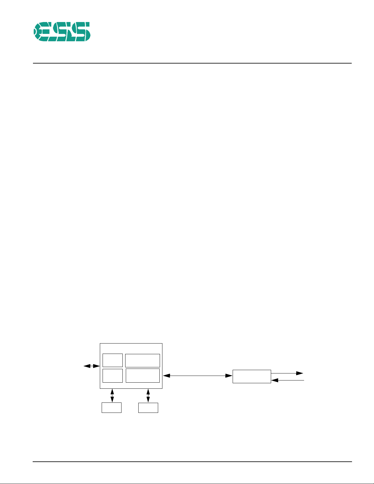
SYSTEM BLOCK DIAGRAM
Figure 1 shows the ES2839/ES2840 system block diagram.
ES2839 HSP MODEM
I/F
LOW-VOLTAGE
DAA
MC‘97
CODEC
XTAL
Figure 1 ES2839/ES2840 System Block Diagram
VOLTAGE DAA
ES2840 HIGH-
PHONE
LINE
PCI AND
MINI PCI
BUS
ESS Technology, Inc. SAM0341-041101 1
PCI I/F
EEPROM
EEPROM
Page 2
PINOUT
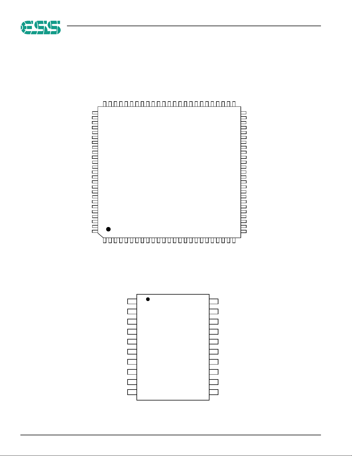
Figure 2 shows the ES2839 and ES2840 pinout diagrams.
D2
VREF
RXN
VCM
RXP
AG ND
KR XN
KR XP
ES2839/ES2840 PRODUCT BRIEF
GN D
VDD
PF7
PF 9
PF8
DSP K / PF11
D5
D3
D4
AV DD
OS CO
D6
GND
GN D
CLKR U N #
VC C
OS CI
D1
KTXP
KTXN
TXN
TXP
AGND
AVDD
VAUX
PF0
PME#
VAUXP
RST#
INTA#
VDD
PCICLK
GND
AD31
AD30
AD29
AD28
AD27
AD26
AD25
AD24
VDD
75747372717069686766656463626160595857565554535251
76
77
78
79
80
81
82
83
84
85
86
87
88
89
90
91
92
93
94
95
96
97
98
99
100
1
2345678
IDSEL
CBE3#
GND
AD23
ES2839S
100-Pin LQFP
9
101112131415161718192021222324
VDD
AD16
AD17
AD18
AD19
AD20
AD21
AD22
GND
IRDY#
CBE 2#
FRAME#
STOP#
TRDY#
DEV SEL#
PAR
CBE1#
50
PF5
49
PF4
48
LCS/PF3
47
PF2
VDD
46
45
SECS
SECLK
44
43
SEDI
42
SEDO
41
GND
40
AD0
AD1
39
AD2
38
AD3
37
AD4
36
AD5
35
AD6
34
AD7
33
VDD
32
31
CBE0#
30
AD8
AD9
29
AD10
28
AD11
27
26
AD12
25
GND
AD1 4
AD1 5
AD1 3
CLIM
D1
D2
VDD
1
2
3
4
20
19
18
17
TOUT
GAIN
LINE
LINEI
ES2840J
D3
D4
LCOM
D5
D6
CPX
5
6
7
8
9
10
20-pin
SSOP
Figure 2 ES2839 and ES2840 Pinout Diagrams
2 SAM0341-041101 ESS Technology, Inc.
16
15
14
13
12
11
INA
INB
TER1
TER2
SET
CPX\
Page 3
ES2839/ES2840 PRODUCT BRIEF
PIN DESCRIPTIONS
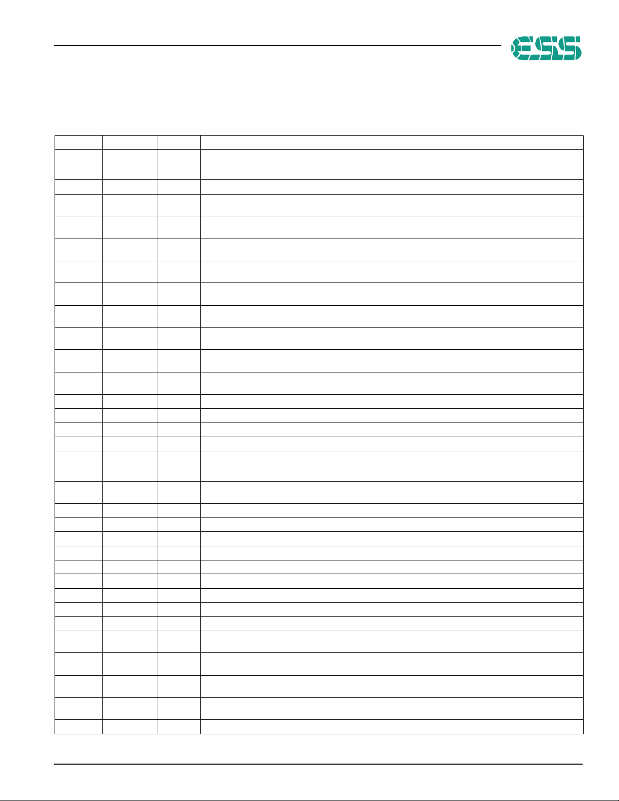
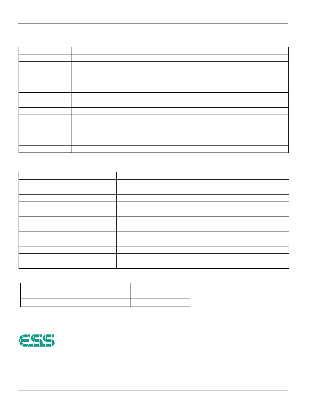
Table 1 lists the ES2839 pin descriptions, and Table 2 lists the
ES2840 pin descriptions.
Table 1 ES2839 Pin Descriptions
Name Pin Number I/O Definitions
C/BE3:0#
IDSEL 2 I Initialization device select, active-high. This pin is used as a chip select during PCI configuration read and write cycles.
GND
AD31:0
VDD
FRAME#
IRDY#
TRDY#
DEVSEL#
STOP#
PAR
SEDO 42 I Serial EPROM data output pin with internal pullup.
SEDI 43 O Serial EPROM data input.
SECLK 44 O Serial EPROM data clock input pin with internal pulldown.
SECS 45 O Serial EPROM chip select pin with internal pulldown.
PF[9:7],
PF[5:4] and
PF[2]
LCS/PF3
DSPK/PF11 57 I/O DSPK/PF11 modem speaker digital output.
OSCI 59 I 18.816-MHz crystal oscillator input.
OSCO 60 O 18.816-MHz crystal oscillator output.
D[6:5] 63, 64 I/O Isolation signal outputs.
AVDD 65, 82 P Analog voltage pins [AVDD (5V)].
AGND 68, 81 G Analog ground.
NC 66, 67, 75, 76 I No connect.
KRXP 69 O Low-voltage DAA analog differential positive output.
KRXN 70 O Low-voltage DAA analog differential negative output.
RXN 71 I Codec analog differential negative input. The DC level is Vcm, and the full-scale input is either 0.22 Vp-p ±5% or 1.1V
RXP 72 I Codec analog differential positive input. The DC level is Vcm, and the full-scale input is either 0.22 Vp-p ±5% or 1.1V
VREF 73 O Voltage reference bypass. Has a range of 1.2356V±5%. Bypass to AGND with 0.1-µF ceramic chip capacitor parallel
VCM 74 O Common mode voltage bypass. Has a range of 2.16V±5%. Bypass to AGND with 0.1-µF ceramic chip capacitor parallel
KTXP 77 I Low-voltage DAA analog differential positive input.
1, 13, 21, 31 I/O Multiplexed bus command/byte enable pins. These pins indicate cycle type during the address phase of a transaction.
3, 15, 22, 41,
52, 61, 64, 91
4:11, 23:30,
33:40, 92:99,
12, 32, 46, 51,
58, 89, 100
14 I/O Cycle frame, active-low. The current PCI bus master drives this pin to indicate the beginning and duration of a
16 I/O Initiator ready, active-low. The current PCI bus master drives this pin to indicate that, as the initiator, it is ready to transmit
17 I/O Target ready, active-low. The current PCI bus master drives this pin to indicate that, as the target device, it is ready to
18 I/O Device select, active-low. The PCI bus target device drives this pin to indicate that it has decoded the address of the
19 I/O Stop transaction, active-low. The current PCI bus target drives this pin active to indicate a request to the master to stop
20 I/O Parity, active-high. Indicates even parity across AD[31:0] and C/BE[3:0]# for both address and data phases. The signal is
47, 49, 50,
55:53,
48 I Local current sense input, pulled to ground through 4.7k Ω resistor. Otherwise, is PF# general-purpose programmable
They indicate active-low byte enable information for the current data phase during the data phases of a transaction.
These pins are inputs during slave operation and outputs during bus mastering operation.
G
Digital ground.
I/O
Address and data pins AD31:0.
P
Digital voltage pins [VDD (3.3V)].
transaction.
or receive data (and complete the current data phase).
transmit or receive data (and complete the current data phase)
current transaction as its own chip select range.
the current transaction.
delayed one PCI clock from either the address or data phase for which parity is generated.
I/O PF2, PF4, PF5, and PF[7:9] general-purpose programmable bidirectional flag pins. Can be used for interfacing with a
telephone or other device, performing such functions as phone-off-hook, phone-on-hook, ring, and caller ID. Refer to pin
descriptions of pins 48 and 57 for preprogrammed telephone interface pins.
flag I/O pin.
p-p±5%, depending on the gain setting.
p-p±5%, depending on the gain setting.
with 10-µF tantalum capacitor.
with 10-µF tantalum capacitor.
ESS Technology, Inc. SAM0341-041101 3
Page 4
ES2839/ES2840 PRODUCT BRIEF
Table 1 ES2839 Pin Descriptions (Continued)
Name Pin Number I/O Definitions
KTXN 78 I Low-voltage DAA analog differential negative input
TXN 79 O Codec negative analog output. The DC level is Vcm, and the full-scale ac output is 2.8V p-p±5%. The maximum loading
TXP 80 O Codec positive analog output. The DC level is Vcm, and the full-scale ac output is 2.8V p-p±5%. The maximum loading is
VAUX
PF0 84 I Pulled to VDD through a 4.7k Ω resistor.
PME# 85 O Power management enable interrupt output to wake up the system.
VAUXP
RST# 87 I Active-low ES2839 reset input.
INTA# 88 O
PCICLK 90 I System bus clock input.
83 I Power to device during implementation of the D3
86 I V
is 1k Ω, in parallel with 20 pF for modem applications. For audio applications with low-impedance load, the maximum
distortion-free (THD <–60-db) current is 10 mA rms.
1k Ω, in parallel with 20 pF for modem applications. For audio applications with low-impedance load, the maximum
distortion-free (THD <–60-db) current is 10 mA rms.
state required by PCI Power Management Interface specification.
cold
support detection. V
AUX
driven low.
Interrupt request, active-low. This pin is the level triggered interrupt pin dedicated to servicing internal device interrupt
sources.
pin is driven high to indicate that ACPI is supported with D3
AUXP
state. No support when
cold
Table 2 ES2840 Pin Descriptions
Names Pin Numbers I/O
CLIM 1 I/O Complex impedance termination pulldown.
D[1:2], D[5:6] 2:3, 8:9 I Isolation signal inputs.
VDR 4 P DC supply input.
D[3:4] 5, 6 O Isolation signal outputs.
LCOM 7 O Line side common ground reference.
CPX, CPX\ 10, 11 I/O DC current limit mode pulldown (pin 10) and 600Ω impedance termination pull-down (pin 11)
SET 12 O DC reference filter.
TER[2:1] 13, 14 I/O Voltage termination controls.
IN{A:B] 15, 16 I Ring and Caller ID signal inputs.
LINEI, LINE 17, 18 I Line AC signal input (pin 17) and line DC signal input (pin 18).
GAIN 19 O Transmit gain control.
TOUT 20 O Transmit gain output.
Definitions
ORDERING INFORMATION
Part Numbers
Descriptions Packages
ES2839S V.90/V.92 PCI HSP Modem 100-pin LQFP
ES2840J Modem High-Voltage DAA 20-pin SSOP
ESS Technology, Inc.
48401 Fremont Blvd.
Fremont, CA 94538
No part of this publication may be reproduced, stored in a
retrieval system, transmitted, or translated in any form or
by any means, electronic, mechanical, manual, optical, or
otherwise, without the prior written permission of ESS
Technology, Inc.
ESS Technology, Inc. makes no representations or
warranties regarding the content of this document.
All specifications are subject to change without prior
notice.
ESS Technology, Inc. assumes no responsibility for any
errors contained herein.
TeleDrive is a registered trademark of ESS Technology, Inc.
(P) U.S. patents pending.
All other trademarks are owned by their respective
holders and are used for identification purposes only.
Tel: (510) 492-1088
Fax: (510) 492-1898
4 © 2001 ESS Technology, Inc. All rights reserved. SAM0341-041101
 Loading...