

Page 1

ESS Technology, Inc. SAM0387-041101 1
ESS Technology, Inc.
ES2841/ES2840
PCI Integrated LAN V.90/V.92 Modem
Product Brief
DESCRIPTION
The ES2841/ES2840, ESS Technology’s first LAN plus hostbased TeleDrive modem chip for the PCI bus, provides desktop
and notebook computers with greater connectivity to both
packet networks and telephone networks. The ES2841/
ES2840 solution uses a solid-state DAA instead of a traditional
transformer DAA. The chipset consists of the ES2841
LAN modem chip and the ES2840, its accompanying highvoltage, solid-state DAA device. The ES2841 maximizes
integration and reduces the external component BOM cost to a
minimum.
The ES2841 device combines into a single-chip a host-based
V.90/V.92 modem, modem control buffers, modem codec, and
an IEEE 802.3-compatible Ethernet media access controller
(MAC) with an analog phoneline interface and a PCI bus
interface. This advanced high-level device integration allows the
ES2841 to be used as a host-based modem and LAN solution for
desktop and notebook systems requiring either a modem
connection or a 10/100 Ethernet connection. The ES2841 is also
capable of providing a home network connection that complies
with the Home Phoneline Networking Alliance (HomePNA) 1-Mb/
s (HPNA1.0) specification.
The ES2841 LAN feature supports 100BASE-TX (100-Mb/s
mode) and 10BASE-T (10-Mb/s mode) full-duplex operations.
The ES2841 includes a media independent interface (MII) and
reduced MII (RMII), enabling it to interface with an external PHY
transceiver used for either a LAN or HPNA-based chipset.
The ES284 modem sends and receives data and fax information
and supports the telephone answering machine (TAM) feature.
With its built-in ACPI D3
cold
wake on-LAN and wake on-ring
support, the ES2841 is an ideal modem solution for notebooks
and battery-operated devices. The ES2841 modem provides the
interface and control logic needed to transfer data between its
serial I/O terminals and the PCI interface.
The ES2841 delivers a high modem connectivity rate and high
throughput without the need of a dedicated DSP. It also
integrates a low-voltage, solid-state DAA that supports both
worldwide homologation and data/fax/voice call discrimination.
With the addition of an external high-voltage, solid-state DAA,
the ES2841 provides a very cost-effective modem/LAN solution
for add-on card, motherboard, and mini-PCI card
implementations.
The ES2840 high-voltage DAA device handles the line
monitoring and filtering functions, while also protecting the
signaling characteristics, performing all of the AC and DC
functions and interfacing with the line side of tip and ring
operations.
The ES2841 is available in a 128-pin low-profile quad flat pack
(LQFP) package. The ES2840 is available in an industry
standard 20-pin super small outline pack (SSOP) package.
FEATURES
• V.90/V.92 analog data/fax/TAM modem
• Data mode capabilities:
—– V.90/V.92: 56 kbps
—– ITU-T V.34: 33.6 kbps and fallbacks
• Fax mode capabilities:
—– ITU-T V.17, V.29, V.27ter, and V.21ch2
—– Group 3 (TIA/EIA-578 Class 1 and Class 2)
• Requires minimum 166-MHz Pentium with MMX technology
• Integrated modem codec and analog front end
• 16-bit ADC and DAC with built-in anti-aliasing and
reconstruction filters
• Integrated low-voltage DAA circuit
• Interface to the ES2840 high-voltage DAA
• 10/100-Mb/s LAN or 1-Mb/s HPNA networking capability
• Integrated on-chip 1/10/100-Mbps MAC controller capable of
interfacing with 10Base-T PHY transceiver and with 100BaseTX PHY transceiver
• MII for connecting to external 10/100-Mbps PHY transceiver
• RMII for connecting to external 10/100-Mbps PHY transceiver
• Full-duplex operation supported in MII and RMII ports with
independent transmit (TX) and receive (RX) channels
• Support for IEEE 802.3x flow control and IEEE 802.3u
autonegotiation for 10Base-T and 100Base-TX
• EEPROM interface for subsystem ID and subsystem vendor ID
• ACPI and PCI power management standard-compliant
• Wake-on-ring and wake-on-LAN capability
• On-chip FIFOs for PCI bus and both RX and TX state machines
• Supports both RJ-11 tip and ring connection and RJ-45 LAN/
Ethernet connection
• PC99/PC2001-compliant with support for V.250, V.251, and
V.253 commands
• Worldwide homologation
MODEM DRIVER SUPPORT
•
Microsoft Windows 98/SE/ME/2000
• Microsoft Windows NT 4.0
LAN DRIVER SUPPORT
•
NIC drivers for Netware 3.x and 4.x networks (16-bit and
32-bit ODI)
• Microsoft Windows networks (NDIS 2.0, 4.0, and 5.0)
• Packet driver
• Linux
Page 2
2 SAM0387-041101 ESS Technology, Inc.
ES2841/ES2840 PRODUCT BRIEF
PINOUT
PINOUT
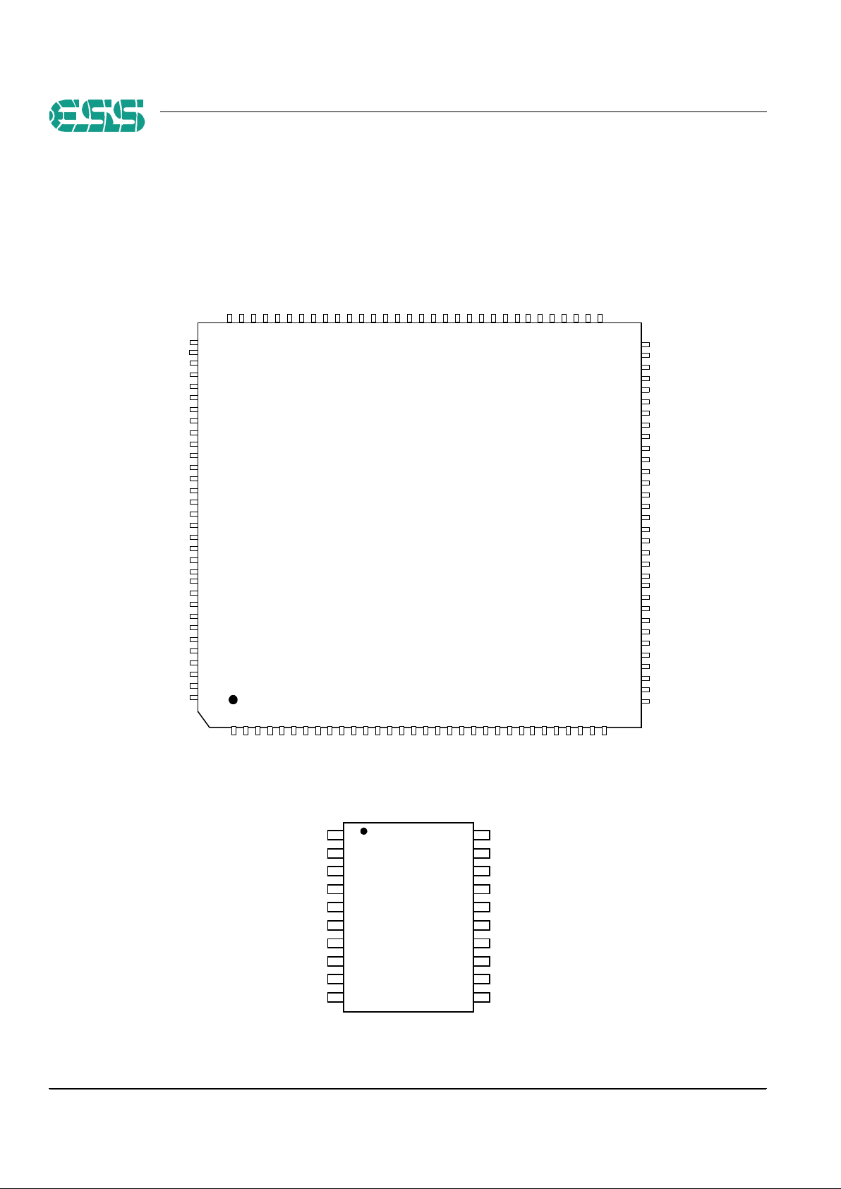
Figure 1 shows the ES2841 and 2840 pinout diagrams.
Figure 1 ES2841 and ES2840 Pinout Diagrams
1
DSPK
PF10
PF9
PF8
KTXP
OSCO
VCM
VREF
RXN
KRXN
KRXP
D3
D4
TXCLK/REFCLK
RXD1
RXD2
VAUX
RXD0
RXER/RX_ER
RXDV/CRS_DV
COL/SPEED10
GND
MDIO/SECLK
MDC/RMII_MODE
RXD3
K_EN/SECS
PF0
TXN
TXP
AGND
AVDD
PF2
PF3
PF4
PF5
TRIDRV
GND
OSCI
LINK_ST2
PWR_RSTB
RST_PHYB
KTXN
D2
ES2841S
AD16
AD17
AD18
AD19
AD21
AD22
AD23
GND
IDSEL
CBE3#
VDD
AD24
AD25
AD28
AD26
AD27
AD29
AD30
AD31
AD3
CBE0#
AD4
IRDY#
GND
FRAME#
CBE2#
VDD
96
97
64
128-Pin LQFP
AD6
AD7
VDD
AD8
AD9
AD10
AD11
AD12
AD13
AD14
AD15
33
32
GN D
CBE1#
PAR
STOP#
DEVSEL#
TRDY#
PME#
VAUXP/WOL
PCICLK
CLKRUN#
PCIGNT#
PCIREQ#
RST#
INTA#
128
VAUX
GND
D1
TXEN
TXD2
65
AD20
AD5
RXP
D5
D6
AD0
AD1
AD2
GND
VAUX
GND
RXCLK
IRQ#
CRS
LINK_ST1
VAUX
PF7
VDD
GND
SERR#
GN D
VDD
VDD
GND
SEDO/TXD0
SEDI/TXD1
TXD3
VAUX
ES2840J
1
2
3
4
5
6
7
8
9
10
20
19
18
17
16
15
14
13
12
11
CLIM
D1
D2
VDD
D3
D4
LCOM
D5
D6
CPX
TOUT
GAIN
LINE
LINEI
INA
INB
TER1
TER2
SET
CPX\
20-pin
SSOP
Page 3
ESS Technology, Inc. SAM0387-041101 3
ES2841/ES2840 PRODUCT BRIEF
PIN DESCRIPTIONS
PIN DESCRIPTIONS
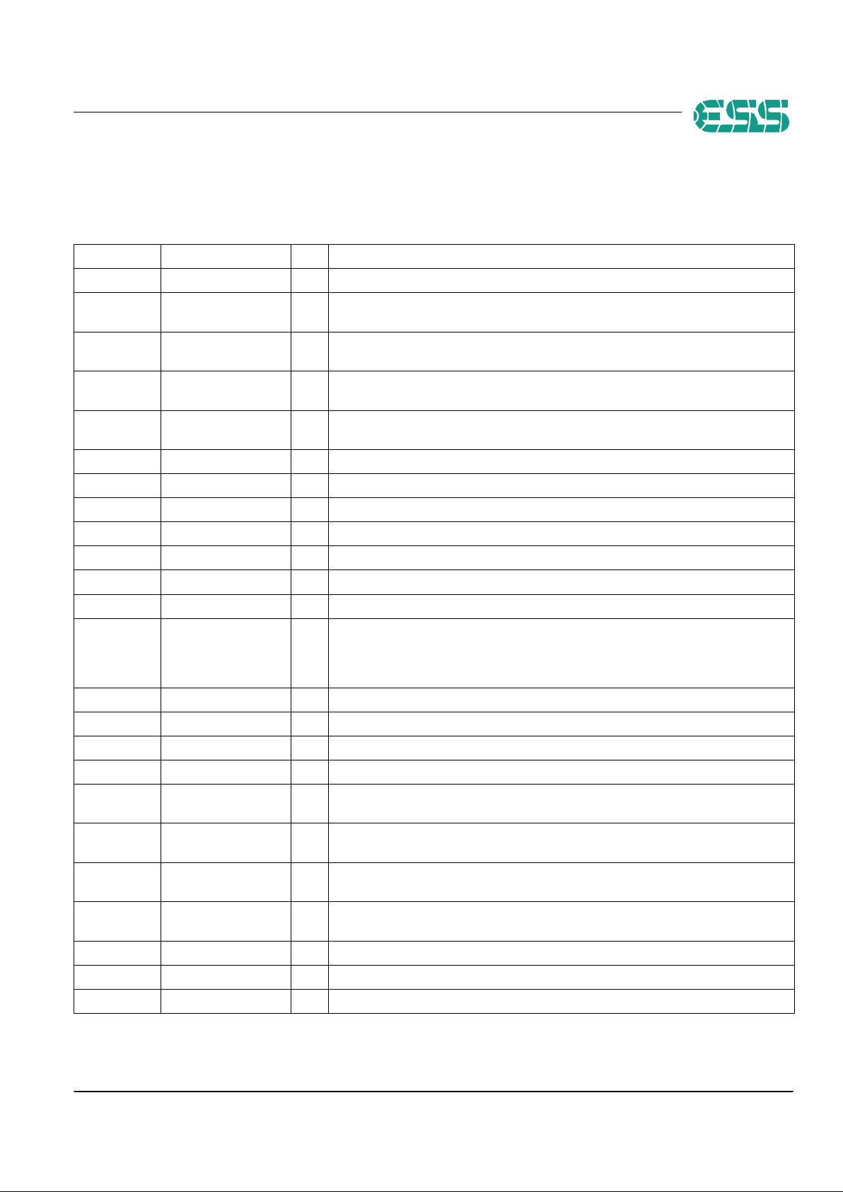
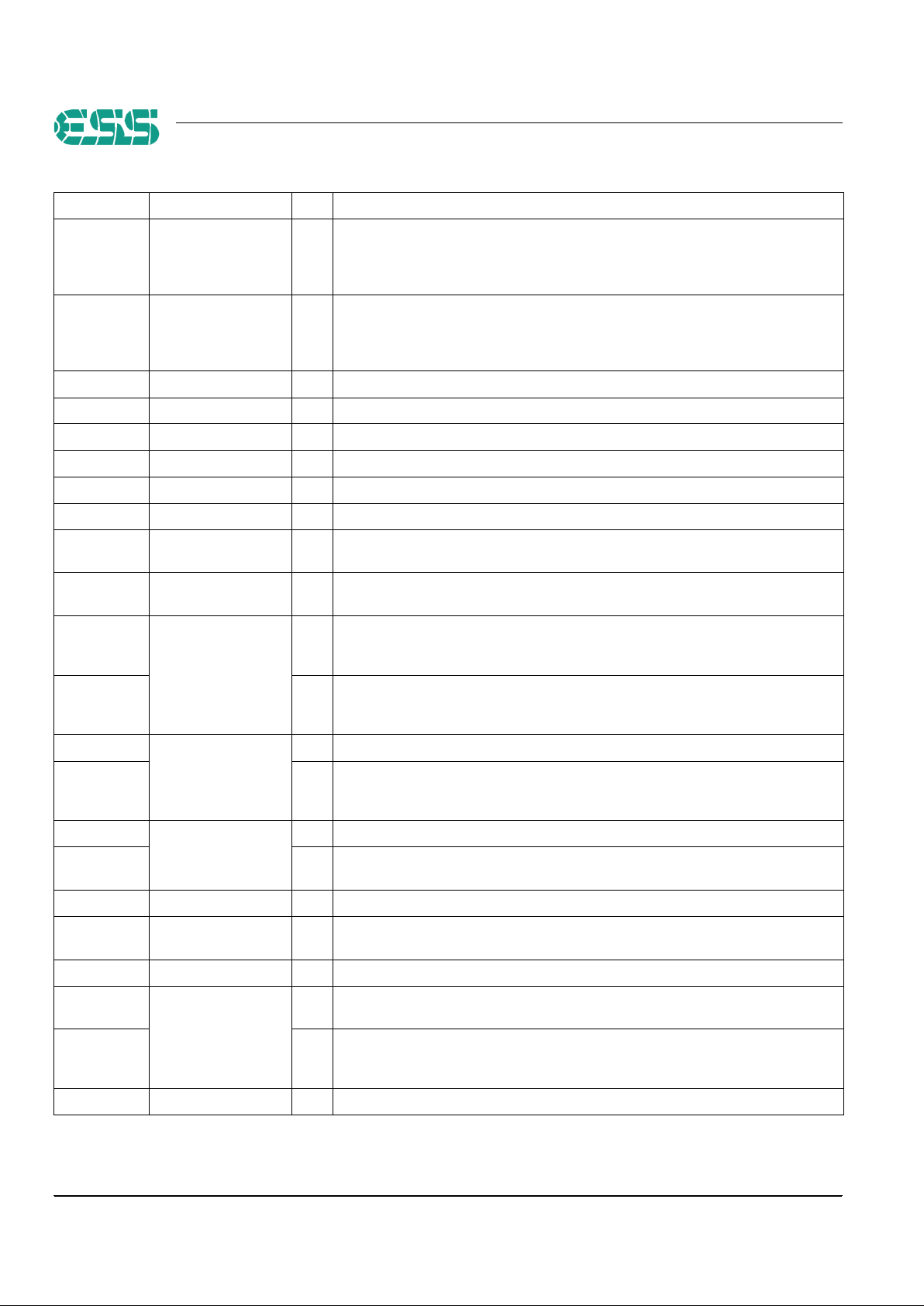
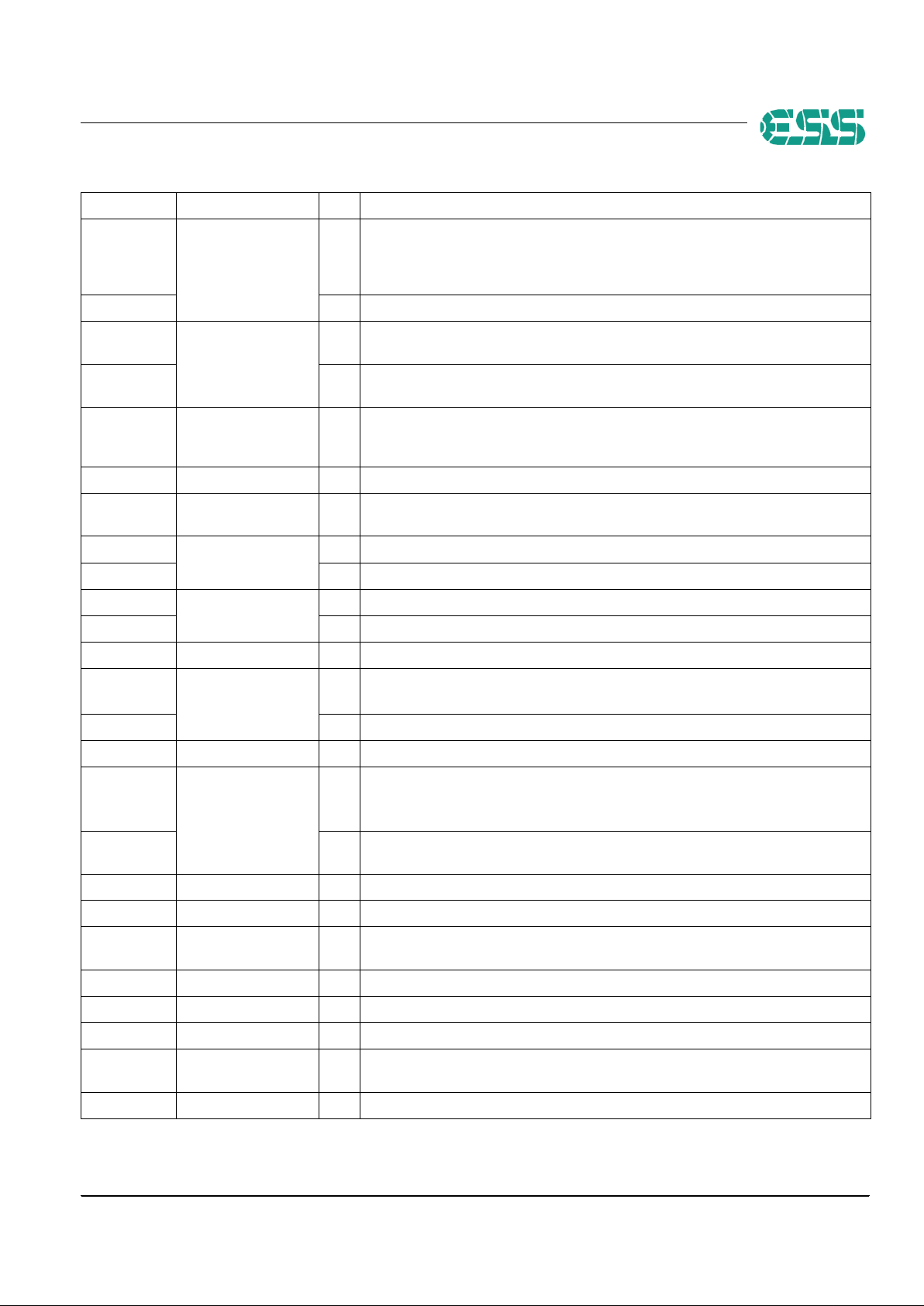
Table 1 lists the ES2841 pin descriptions, and Table 2 lists
the ES2840 pin descriptions.
Table 1 ES2841 Pin Descriptions
Names Pin Numbers I/O Definitions
IDSEL 1 I ID select.
GND 2, 3, 22, 23, 52, 53,
72, 85, 86, 116, 117
G Digital ground.
VDD 12, 13, 37, 38, 126,
127
P 3.3V digital power supply.
AD[31:0] 4:11, 24:28, 33:35,
39:46, 118:125
I/O Address and data lines from the PCI bus.
C/BE[3:0]# 14, 21, 36, 128 I/O PCI command/byte enable. During address phase of a transaction, these pins
define the bus command. During data phase, these pins define the bus enable.
FRAME# 15 I/O Cycle frame.
IRDY# 16 I/O Initiator ready.
TRDY# 17 I/O Target ready.
DEVSEL# 18 I/O Device select.
STOP# 19 I/O Stop transaction.
PAR 20 I/O Parity.
SERR# 29 OD System bus error.
PF[10:7] and
PF[5:2]
30:32, 47:51 I/O General-purpose programmable bidirectional flag. These pins can be used for
interfacing with a telephone or other device, performing such functions as caller ID,
etc. Refer to pin descriptions for pins 54, 108, and 109 for preprogrammed
telephone interface pins.
D5 and D6 54, 55 O D6 isolation signal output.
D[4:3] 56, 57 I Receive data signal inputs from external hybrid interface.
KRXP 58 O DAA analog differential receive positive output.
KRXN 59 O DAA analog differential receive negative output.
RXN 60 I Codec analog differential receive negative input. The DC level is VCM, and the full-
scale input is either 2.2Vp-p±5% or 1.1Vp-p±5%, depending on the gain setting.
RXP 61 I Codec analog differential receive positive input. The DC level is VCM, and the full-
scale input is either 2.2Vp-p±5% or 1.1Vp-p±5%, depending on the gain setting.
VREF 62 O Voltage reference bypass. Has a range of 1.235V±5%. Bypass to AGND with
0.1-mF ceramic chip capacitor parallel with 10-mF tantalum capacitor.
VCM 63 O Common mode voltage bypass. Has a range of 2.16V±5%. Bypass to AGND with
0.1-mF ceramic chip capacitor parallel with 10-mF tantalum capacitor.
D[2:1] 64, 65 O Transmit signal outputs to external hybrid interface.
KTXP 66 I DAA analog differential transmit positive input.
KTXN 67 I DAA analog differential transmit negative input.
Page 4
4 SAM0387-041101 ESS Technology, Inc.
ES2841/ES2840 PRODUCT BRIEF
PIN DESCRIPTIONS
TXN 68 O Codec analog differential transmit negative output. The DC level is VCM, and the
full-scale input is either 2.8Vp-p±5% or 1.4Vp-p±5%, depending on the gain
setting.The maximum loading is 1.2k W, in parallel with 20 pF for modem
applications.
TXP 69 O Codec analog differential transmit positive output. The DC level is VCM, and the
full-scale input is either 2.8Vp-p±5% or 1.4Vp-p±5%, depending on the gain
setting.The maximum loading is 1.2k W, in parallel with 20 pF for modem
applications.
AGND 70 G Analog ground.
AVDD 71 P 5V analog power supply.
OSCI 73 I Crystal clock input.
OSCO 74 O Crystal clock output.
VAUX 75, 88, 89, 104, 105 P 3.3V VAUX power supply for wake-on-ring and wake-on-LAN.
LINK_ST1 76 I Link status interface input from PHY.
PHY_RSTB 77 O Reset output to PHY; will follow PWR_RSTB and remain active for 1.3 msec after
PWR_RSTB. Can be toggled by bit 7 of LAN_IO register [4Ah].
PWR_RSTB 78 I Power-on reset. This is an active-low input signal when a power-on reset event
occurs.
RXER
79
I Receive error input for MII mode. Indicates that external PHY transceiver has
detected coding errors in receive data frame currently being transmitted to
RXD[3:0]. RXER is ignored while RX_DV is deasserted.
RX_ER I Receive error input for RMII mode. Indicates that external PHY transceiver has
detected coding errors in receive data frame currently being transmitted to
RXD[1:0]. RX_ER is ignored while RX_DV is deasserted.
RXDV
80
I Receive data valid.
CRS_DV I Carrier sense/receive data valid. Asserted asynchronously by the PHY when the
receive medium is nonidle. In 10Base-T mode, carrier is detected when squelch is
passed in RMII mode.
COL
81
I Collision. When selected as COL, asserted output whenever a collision is detected.
SPEED10 I Speed select pin. Acts as toggle for 10-Mb/s and 100-Mb/s operation for external
PHY transceiver in RMII mode.
CRS 82 I Carrier sense input.
RXCLK 83 I Receive clock input. Provides the nibble rate clock timing reference for the output
transfer of RXDV, RXD[3:0] and RXER/RX_ER signals and operates at 25/2.5 MHz.
IRQ# 84 I Interrupt request.
TXCLK
87
I Transmit clock input. When selected as TXCLK, provides timing reference for
transfer of the transmitted data and operates at 25/2.5 MHz.
REFCLK I Reference clock input. When selected as REFCLK, provides continuous clock
timing reference for CRS_DV, RXD[1:0], TXEN, TXD[1:0], and RX_ER. Operates at
50 MHz ±50 ppm, with a duty cycle between 35% and 65% in RMII mode.
RXD[3:0] 90:93 I Receive data pins [3:0]. When in RMII mode, only RXD[1:0] are defined.
Table 1 ES2841 Pin Descriptions (Continued)
Names Pin Numbers I/O Definitions
Page 5
ESS Technology, Inc. SAM0387-041101 5
ES2841/ES2840 PRODUCT BRIEF
PIN DESCRIPTIONS
MDIO
94
I/O When the MDIO function is selected, this pin functions as the MII management data
I/O pin. It acts as an output during the header portion of management frame
transfers and during the data portion of write operations. It also acts as an input dur-
ing the data portion of read operations.
SECLK O Serial EEPROM data clock input.
MDC
95
O When the MDC function is selected, this pin functions as the MII management data
clock pin. It runs up to 2.5 MHz.
RMII_MODE I RMII_MODE enable. The ES2841 supports both MII and RMII modes. When the
RMII_MODE signal is high, RMII mode is supported.
TRIDRV 96 O Tri-state output pin connected to the input pin of HPNA PHY to tri-state output of
HPNA PHY. When asserted high, this pin tri-states all outputs except open-drain
outputs.
LINK_ST2 97 I Link status interface input from (second) HPNA PHY.
TXEN 98 O Transmit enable. Indicates that the MAC is presenting valid data on TXD[3:0].
TXEN transitions are latched on the falling edge of REFCLK.
SEDO
99
O Serial EEPROM data input.
TXD[0] O Transmit data output pin 0.
SEDI
100
I Serial EEPROM data output pin with an internal pullup.
TXD[1] O Transmit data output pin 1.
TXD[3:2] 101, 102 O Transmit data pins 2 and 3 in MII mode. Not defined in RMII mode.
K_EN
103
I On-chip low-voltage DAA enable input. Pullup to V
AUX
to enable the on-chip low-
voltage DAA module. Strap option pin latched at power-on reset.
SECS O Serial EEPROM port chip select output.
PME# 106 OD Power management enable interrupt output to wake up the system.
VAUXP
107
I V
AUX
support detection pin. V
AUXP
is driven high at reset to indicate that ACPI is
supported with D3
cold
state. No support when driven low. Strap option pin latched
at power-on reset.
WOL O Wake-on-LAN signal output. The ES2841 asserts this signal if a change is detected
in link status, Magic Packet, or sample frame events.
PF0 108 I General-purpose programmable input pin 0.
DSPK 109 O Modem speaker digital output when selected.
CLKRUN# 110 I/O CLKRUN# is an I/O pin for PCI clock status and an output to start or accelerate
clock function.
PCIGNT# 111 I PCI grant input.
PCIREQ# 112 O PCI request output.
RST# 113 I PCI bus reset.
INTA# 114 OD Interrupt A request output, active-low. INTA# is the level triggered interrupt pin ded-
icated to servicing internal device interrupt requests.
PCICLK 115 I PCI bus clock input.
Table 1 ES2841 Pin Descriptions (Continued)
Names Pin Numbers I/O Definitions
Page 6
6 © 2001 ESS Technology, Inc. SAM0387-041101
ES2841/ES2840 PRODUCT BRIEF
ORDERING INFORMATION
No part of this publication may be reproduced, stored in a
retrieval system, transmitted, or translated in any form or
by any means, electronic, mechanical, manual, optical, or
otherwise, without the prior written permission of ESS
Technology, Inc.
ESS Technology, Inc. makes no representations or
warranties regarding the content of this document.
All specifications are subject to change without prior
notice.
ESS Technology, Inc. assumes no responsibility for any
errors contained herein.
(P) U.S. patents pending.
TeleDrive is a registered trademark of ESS Technology,
Inc.
All other trademarks are owned by their respective
holders and are used for identification purposes only.
ESS Technology, Inc.
48401 Fremont Blvd.
Fremont, CA 94538
Tel: (510) 492-1088
Fax: (510) 492-1898
ORDERING INFORMATION
Table 2 ES2840 Pin Description
Name Pin Numbers I/O
Definitions
CLIM 1 I/O Complex impedance termination pulldown.
D[1:2], D[5:6] 2:3, 8:9 I Isolation signal inputs.
VDR 4 P DC supply input.
D[3:4] 5, 6 O Isolation signal outputs.
LCOM 7 O Line side common ground reference.
CPX, CPX\ 10, 11 I/O DC current limit mode pulldown (pin 10) and 600Ω impedance termination pull-
down (pin 11)
SET 12 O DC reference filter.
TER[2:1] 13, 14 I/O Voltage termination controls.
IN{A:B] 15, 16 I Ring and caller ID signal inputs.
LINEI, LINE 17, 18 I Line AC signal input (pin 17) and line DC signal input (pin 18).
GAIN 19 O Transmit gain control.
TOUT 20 O Transmit gain output.
Part Numbers
Descriptions Packages
ES2841S PCI V.90/V.92 HSP Modem
LAN
128-pin LQFP
ES2840J Modem High-Voltage DAA 20-pin SSOP
 Loading...