

Page 1
ES2828
Modem Analog Front End
ESS Technology, Inc.
DESCRIPTION
The ES2828 TeleDrive modem chip is an analog-front-end (AFE)
chip designed to work with ESS Technology modem DSPs and
audio-accelerator chips, as well as with system core-logic
chipsets, to offer the most versatile solution for modems only or
for complete audio-modem combinations. With the addition of an
external transformer DAA, the ES2828 modem AFE chip
provides a very low-cost, complete host-based modem solution.
The ES2828 modem provides high performance, high
connectivity, and high throughput. It integrates a low-pass
continuous anti-aliasing filter, a 16-bit resolution ADC, a 16-bit
DAC, a low-pass output-reconstruction filter, and an AC-Link
interface for core-logic chipset-based modem solution.
The ES2828 includes ADC and DAC signal processing channels
and the associated data controls for each channel. The two
channels operate synchronously, so that data reception at the
ADC channel and data transmission from the DAC channel occur
during the same time interval.
The ES2828 modem solution is capable of send/receive data
and fax, supports telephone answering machine (TAM), and is
capable of data/fax/voice call discrimination. With its built-in
ACPI and D3
modem solution for notebooks and battery-operated devices.
The ES2828 modem solution meets all the requirements for
Microsoft WHQL certification, as well as V.250, V.251, and V.253
commands
The ES2828 is available in an industry-standard 48-pin lowprofile quad flat pack (LQFP) package.
wake-on-ring support, the ES2828 is an ideal
cold
Product Brief
FEATURES
• V.90/V.92 analog data/fax/TAM modem
• Data Mode capabilities:
—– V.90/V.92: 56 kbps
—– ITU-T V.34: 33.6 kbps and fallbacks
• Fax mode capabilities:
—– ITU-T V.17, V.29, V.27ter, and V.21ch2
—– Group 3 (TIA/EIA-578 Class 1 and Class 2)
• Requires minimum 166-MHz Pentium with MMX technology
• PC99/PC2001-compliant with support for V.250, V.251, and
V.253 commands
• V.80 (H.324 software-stack-compatible)
• MC‘97-compliant modem codec supporting AC-Link compatible
with Rev 2.1 of the Intel™ AC‘97 specification
• Sigma-delta modulation codec
• Software reset through command register
• Caller ID
• Data/fax/voice call discrimination
• Worldwide homologation
• 16-bit ADC and DAC with built-in anti-aliasing and
reconstruction filters
• Compliance with ACPI 1.0 and PCI Power Management
Interface 1.0, supporting the D3
• Supports Microsoft Windows Unimodem V and TAPI
specifications
• Supports Microsoft Windows 98/SE/ME/2000
• Supports Windows NT 4.0
wake-on-ring
cold
BLOCK DIAGRAMS
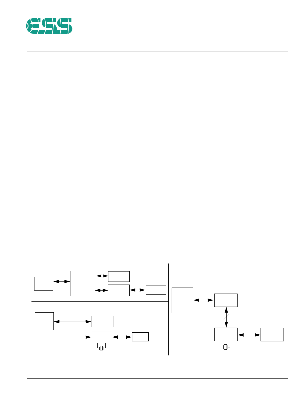
Figure 1 shows the ES2828 block diagrams.
ESS AUDIO MODEM COMBO DESIGN
ES2828
ES1921 AC‘97
Audio Codec
ES2828
Modem AFE
DAA
DAA
HOST PCI
BUS
INTERFACE
CORE-LOGIC CHIPSET-BASED MODEM DESIGN
CORELOGIC
CHIPSET
AC-Link #1
ES1980
Audio Accelerator
AC-Link #2
AC-Link
ES1921 AC‘97
Audio Codec
Modem AFE
24.576 MHz
Figure 1 ES2828 Block Diagrams
ESS Technology, Inc. SAM0315-041101 1
ESS DSP MODEM DESIGN
(CHI BUS MODE)
HOST
PCI
BUS
INTERFACE
ES2898
TeleDrive
CHI BUS
ES2828
Modem AFE
4
DAA
18.816 MHz
Page 2
PINOUT
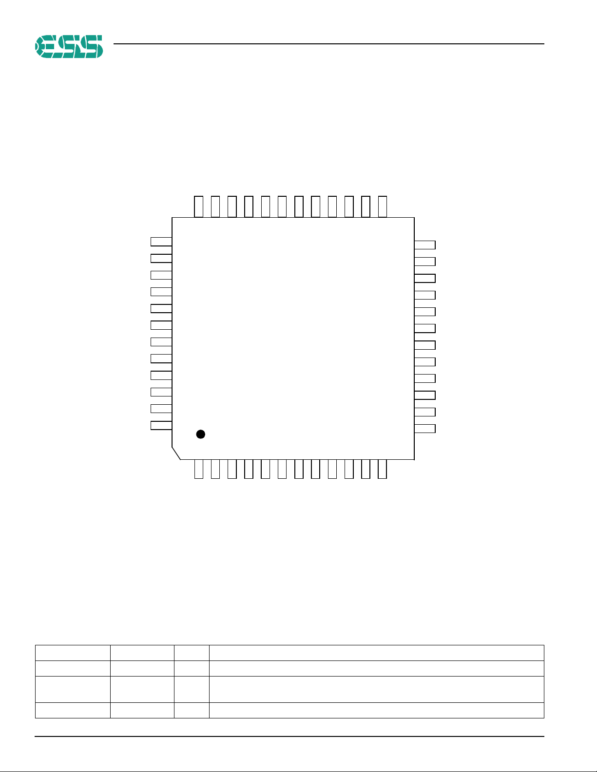
Figure 2 shows the ES2828 pinout diagram.
ES2828 PRODUCT BRIEF
SO
SC/BITCLK
FS/SYNC
CKO
DVDD
XTALO
ID0
SDATA_IN
ID1
PWDN#
XTALI
RST#
VAUX
RING#/GPIO_0
CALLID/GPIO_1
GPIO_2
LCS/GPIO_3
GPIO_4
GPIO_5
DGND
OFFHK/GPIO_6
GPIO_7
GPIO_8
GPIO_9
36 35 34 33 32 31 30 29 27 2628
37
38
39
40
41
42
43
44
45
46
47
48
1
2 3 4 5 6 7 8 9 10 11 12
DPBX
ES2828S
48-PIN LQFP
DVDD
AGND
AGND
AGND
25
24
23
22
21
20
19
18
17
16
15
14
13
AUX-
AUX+
RXIN-
RXIN+
VCM
AVDD
SI/SDATA_OUT
DVDD
CTST
DGND
HCT
VCMX
AGND
TXTX+
VRBP
VREF
VCBP
ACLINK/GPIO_B
Figure 2 ES2828 Pinout Diagram
ES2828 PIN DESCRIPTION
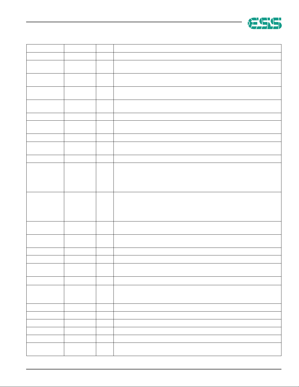
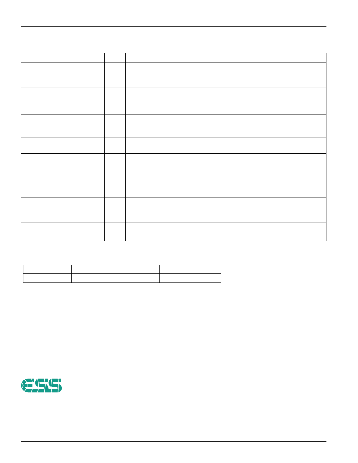
Table 1 lists the ES2828 pin descriptions.
Table 1 ES2828 Pin Descriptions
Names Pin Numbers I/O Definitions
DPBX 1 I Digital PBX detection.
ACLINK/GPIO_B 2 I/O Bus strap pin. Default is CHI Bus (internal pulldown). To implement AC-Link mode,
use a 10k Ω pullup resistor.
DVDD 3, 23, 29 P 3.3V digital power.
2 SAM0315-041101 ESS Technology, Inc.
Page 3
ES2828 PRODUCT BRIEF
Table 1 ES2828 Pin Descriptions (Continued)
Names Pin Numbers I/O Definitions
AGND 4:6, 18 I Analog ground.
AUX+ 7 I Codec analog auxiliary differential positive input. The DC level is Vcm, and the full-
scale input is either 2.2Vp-p ±5% or 1.1Vp-p±5%, depending on the gain setting.
AUX- 8 I Codec analog auxiliary differential negative input. The DC level is Vcm, and the full-
scale input is either 2.2Vp-p ±5% or 1.1Vp-p±5%, depending on the gain setting.
RXIN+ 9 I Codec analog differential positive input. The DC level is Vcm, and the full-scale input
is either 2.2Vp-p ±5% or 1.1Vp-p±5%, depending on the gain setting.
RXIN- 10 I Codec analog differential negative input. The DC level is Vcm, and the full-scale
input is either 2.2Vp-p ±5% or 1.1Vp-p±5%, depending on the gain setting.
AVDD 11 I Analog 5.0V supply.
VCM 12 O Common mode voltage bypass. Has a range of 2.16V±5%. Bypass to VCBP with
0.1-µF ceramic chip capacitor parallel with 10-µF tantalum capacitor.
VCBP 13 I Ground pin for VCM.
VREF 14 O Voltage reference bypass. Has a range of 1.2356V±5%. Bypass to GND2 with 0.1-
µF ceramic chip capacitor parallel with 10-µF tantalum capacitor.
VRBP 15 I Ground pin for VREF.
TX+ 16 O Codec positive analog output. The DC level is Vcm, and the full-scale ac output is
either 2.8Vp-p±5% or 1.4V p-p±5%, depending on the gain setting. The maximum
loading is 20k Ω in parallel with 20 pF for modem applications. For audio applications
with low-impedance load, the maximum distortion-free (THD <–60 db) current is
10 mA rms.
TX- 17 O Codec negative analog output. The DC level is Vcm, and the full-scale ac output is
either 2.8Vp-p±5% or 1.4V p-p±5%, depending on the gain setting. The maximum
loading is 20 kΩ in parallel with 20 pF for modem applications. For audio applications
with low-impedance load, the maximum distortion-free (THD <–60 db) current is
10 mA rms.
VCMX 19 O Codec common mode reference voltage output pin. 2.16V±5%, maximum, current
±500 µA, maximum, capacitive load 20 pF.
HCT 20 I Codec digital input mode control pin. The CHI bus interface uses a 4.7k Ω pulldown
resistor. The AC-Link interface uses a 10k Ω pullup resistor.
DGND 21, 44 — Digital ground.
CTST 22 I Codec sigma delta modulator test port output enable.
SI/SDATA_OUT 24 I Serial port input (default). In AC-Link mode, is AC‘97 serial data input pin. To use in
CHI bus mode, use a 4.7k Ω pulldown resistor.
SO 25 O Serial port output without V
SC/BITCLK 26 I/O, O Serial port clock output. While input must be TTL-compatible, should be able to
handle 3.3V input. In AC-Link mode, is 12.288 MHz serial data clock BITCLK output
or input for secondary codecs, depending on codec configuration.
FS/SYNC 27 O Serial port frame sync. In AC-Link mode, is 48-kHz fixed-rate sample sync.
CKO 28 O 3.3V clock output.
XTALO 30 O 24.576-MHz crystal oscillator output.
XTALI 31 I 24.576-MHz crystal oscillator input.
RST# 32 I Reset.
ID1 33 I Modem AFE configuration strap pin 1. When pulled down internally with ID0 pin 35,
helps set primary and secondary modem codec ID configuration.
AUX
support.
ESS Technology, Inc. SAM0315-041101 3
Page 4
ES2828 PRODUCT BRIEF
Table 1 ES2828 Pin Descriptions (Continued)
Names Pin Numbers I/O Definitions
PWDN# 34 I Power-down (active-low) (CHI Bus mode only).
ID0 35 I Modem AFE configuration strap pin 0. When pulled down internally with ID1 pin 33,
helps set primary and secondary modem codec ID configuration.
SDATA_IN 36 O Serial data output. Serial port output with V
V
AUX
37 I Power to device during implementation of the D3
Management Interface specification.
RING#/GPIO_0 38 I/O Ring in detection (default). This pin is used for ring detect input during the D3
state to drive the device back to its default power-up state. In AC-Link mode, is
GPIO_0 input/output.
CALLID/GPIO_1 39 I,
Caller ID (default output). Otherwise, is GPIO_1 input/output.
I/O
GPIO_2 40 I/O Voice relay control (output).
LCS/GPIO_3 41 I,
Loop current sense (default input). Otherwise, is GPIO_3 input/output.
I/O
GPIO_4 42 I/O Ring sensitivity (RISEN#) Control. (International DAA) (output).
GPIO_5 43 I/O Pulse dialing control (output).
OFFHK/GPIO_6 45 O,
Off-hook relay control (default output). Otherwise, is GPIO_6 input/output.
I/O
GPIO_7 46 I/O Current limit control (output).
GPIO_8 47 I/O Complex impedance mach control (output).
GPIO_9 48 I/O General-purpose input/output.
AUX
support.
state required by PCI Power
cold
cold
ORDERING INFORMATION
Part Number
Description Package
ES2828S Modem Analog Front End 48-pin LQFP
No part of this publication may be reproduced, stored in a
retrieval system, transmitted, or translated in any form or
by any means, electronic, mechanical, manual, optical, or
otherwise, without the prior written permission of ESS
ESS Technology, Inc.
48401 Fremont Blvd.
Fremont, CA 94538
Technology, Inc.
ESS Technology, Inc. makes no representations or
warranties regarding the content of this document.
All specifications are subject to change without prior
notice.
Tel: (510) 492-1088
Fax: (510) 492-1898
ESS Technology, Inc. assumes no responsibility for any
errors contained herein.
TeleDrive is a registered trademark of ESS Technology, Inc.
(P) U.S. patents pending.
All other trademarks are owned by their respective
holders and are used for identification purposes only.
4 © 2001 ESS Technology, Inc. All rights reserved. SAM0315-041101
 Loading...