

Page 1

VisbaTM ES3883
Video CD Companion Chip
ESS Technology, Inc.
DESCRIPTION
The Visba ES3883 video CD companion chip (CC) is the
second-generation companion chip that provides an optimal
system design for a video CD player when used with the Visba
ES3880 video CD PC. The ES3883 Visba video CD CC
integrates the CD-ROM controller (featuring direct servo control),
as well as most of the required analog discrete components, into
a simple, highly cost-effective design for a video CD player. The
Visba video CD CC provides the best quality for both video and
audio, and easily passes the highest graded level for the China
VCD standard.
The Visba video CD CC features include a high-quality NTSC/
PAL digital video encoder (DVE), echo, surround sound, audio
DACs, and PLL clock synthesizer. Additionally, there are also
three 9-bit video DACs and two 16-bit sigma-delta audio DACs.
One video DAC handles composite video output, while the other
two handle the S-video outputs. The two 16-bit sigma-delta audio
DACs offer differential outputs. The differential dual audio
outputs from these audio DACs ensure further noise reduction to
a minimum of 90 dB, enabling the Visba video CD CC to pass the
best quality audio on all video CD parameter specifications.
The DVE generates composite and S-video analog signals.
Color space conversions (CSCs) are provided to match the input
data to the required output format. Then, the data is filtered to
meet the selected video standards. In addition, the Visba video
CD CC is equipped with a remote control interface for power
standby on/off, two microphone ports, auxiliary ports, and an
interface for accessing internal registers.
The ES3883 is available in an industry-standard 100-pin plastic
quad flat pack (PQFP) package.
Product Brief
FEATURES
• Multistandard TV encoder:
— CCIR601 nonsquare operation
— NTSC/PAL formats
— Master video mode
— 8-bit interface for YCrCb (4:2:2) input format
— Simultaneous composite and S-video output
— Interlaced operation
• Audio DACs:
— Two 16-bit sigma-delta DACs
— Dual audio output, SNR better than 90 dB
— Accepts I2S format data
— Programmable functions
• Surround sound
• Remote control interface for power standby on/off
• Digitally controlled echo with up to 130-ms delay
• Dual microphone input
• Clock synthesizer (PLL):
— Based on 27-MHz crystal input
— Generates required clocks for video encoder, audio
DAC, echo and surround sound, and video processor
• Device serial communication (DSC) port for command issued/
register access
• Graphical user interface (GUI) and hyperlink
• Direct CD servo control
• Vocal assist
• Remote control
• Interrupt control
• Power management
• 100-pin PQFP
• Single 5V power supply
Figure 1 shows a block diagram of a standalone system with a
Visba video CD processor chip and a video CD companion chip.
Visba ES3883
Companion Chip
CD-ROM Controller
CD-ROM
Kit
ROM
Visba ES3880
(Video CD)
DRAM
Mic 1
Mic 2
Remote
Control
DSC
PLL
Echo/Surround/Vocal Assist
Preamp
Volume Control
Preamp
Volume Control
Figure 1 Visba ES3883 Video CD Companion Chip System Block Diagram
ESS Technology, Inc. SAM0416-052201 1
Interrupt
Control
Audio DAC
NTSC/PAL Video
VFD
Driver
VFD
Panel
Remote
Receiver
Speakers
Television
Page 2
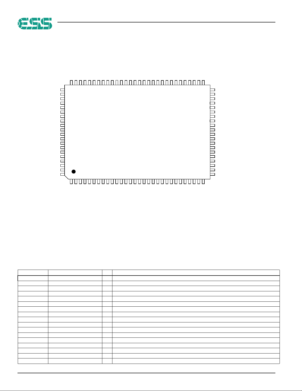
PINOUT
Figure 2 shows the Visba ES 3883 pinout diagram.
XOUT
VSS
VCC
XIN
VSS
NC
VSS
VCC
PCLK
2XPCLK
ES3883 PRODUCT BRIEF
YDAC
VSSAV
VSSAV
VDAC
ACAP
VCC
AUX6/VFD_DO
AUX5
AUX4
AUX3
VCCAV
VCCAV
COMP
VSSAV
VSSAV
CDAC
VSSAA
VREF
VREFM
RSET
DSC_D7
HSYN_B
DSC_D6
VSYN_B
DSC_D5
YUV7
YUV6
YUV5
YUV4
VCC
VSS
YUV3
DSC_D4
YUV2
DSC_D3
YUV1
DSC_D2
YUV0
DSC_D1
VSS
80
79 78 77 76 75 74 73 72 71 70 69 68 67 66 65 64 63 62 61 60 59 58 57 56 55 54 53 52
81
82
83
84
85
86
87
88
89
90
91
92
93
94
95
96
97
98
99
100
1
2 3 4 5 6 7 8 9 10 11 12 13 14 15 16 17 18 19 20 21 22 23 24 25 26 27 28 29
NC
NC
VSS
Visba ES3883
Video CD
Companion Chip
100-Pin PQFP
NC
VCC
AUX0
DSC_C
AUX2
AUX1
DSC_S
DSC_D0
DCLK/EXT_CLK
VCC
MCLK
MUTE
RESET_B
AUX7/VFD_DI
TSD
TBCK
AUX9/SQS0
AUX8/VFD_CLK
TWS/SPLL_OUT
RSTOUT_B
RWS/SEL_PLL1
51
MIC2
50
MIC1
49
AOL+
48
AOL-
47
AOR-
46
AOR+
45
VCCAA
44
VREFP
43
VCM
42
VSSAA
41
AUX15/IR
40
AUX14/SOS1
39
AUX13/SP
38
RBCK/SER_IN
37
AUX12/C2PO
36
AUX11/IRQ
35
AUX10/SQCK
34
33
RSD/SEL_PLL0
32
VCC
31
VSS
30
NC
NC
NC
NC
VSS
VSS
Figure 2 Visba ES883 Pinout Diagram
VISBA ES3883 PIN DESCRIPTIONS
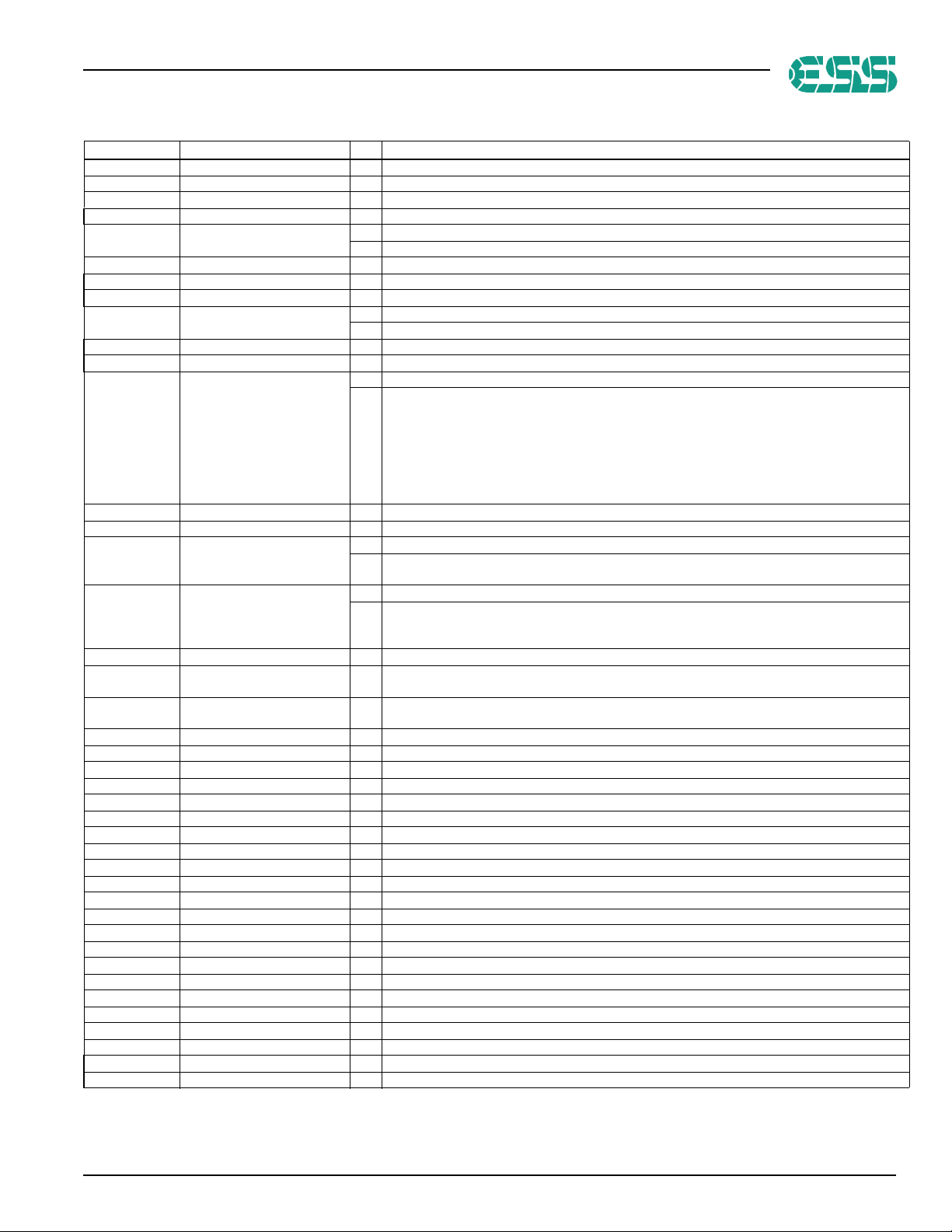
Table 1 lists the Visba ES3883 pin descriptions.
Table 1 Visba ES3883 Pin Description
Name Number I/O Definition
VSS 1,25:26,31,72,75,77,91,100 I Ground.
VCC 5,16,32,66,73,78,90 I Voltage supply, 5V.
DSC_C 6 I Clock for programming to access internal registers.
AUX0 7 I/O Servo forward or general-purpose I/O.
AUX1 9 I/O Servo reverse or general-purpose I/O.
AUX2 11 I/O Servo LDON or general-purpose I/O.
AUX3 70 I/O Servo CW/limit or general-purpose I/O.
AUX4 69 I/O Servo CCW/close or general-purpose I/O.
AUX5 68 I/O Servo data or general-purpose I/O.
AUX6 67 I/O Servo XLAT or general-purpose I/O/VFD_DO.
AUX7 14 I/O Servo BRKM/sense or general-purpose I/O/VFD_DI.
AUX8 18 I/O Servo mute/open or general-purpose I/O/VFD_CLK.
AUX9 20 I/O Servo SQS0 or general-purpose I/O.
AUX10 34 I/O Servo SQCK or general-purpose I/O.
AUX11 35 I/O 3880 IRQ or interrupt output or general-purpose I/O.
AUX12 36 I/O CD C2PO or interrupt input or general-purpose I/O.
AUX13 38 I/O Serial interrupt/CD-mute or general-purpose I/O.
2 SAM0416-052201 ESS Technology, Inc.
Page 3
ES3883 PRODUCT BRIEF
Table 1 Visba ES3883 Pin Description (Continued)
Name Number I/O Definition
AUX14 39 I/O Servo SCOR (S0S1), interrupt input, or general-purpose I/O.
AUX15 40 I/O Interrupt input or general-purpose I/O.
DSC_D[7:0] 81,83,85,93,95,97,99,8 I/O Data for programming to access internal registers.
DSC_S 10 I Strobe for programming to access internal registers.
DCLK
EXT_CLK I EXT_CLK is the external clock. EXT_CLK is an input during bypass PLL mode.
RESET_B 13 I Video reset (active-low).
MUTE 15 O Audio mute.
MCLK 17 I Audio master clock.
TWS
SPLL_OUT O SPLL_OUT is the select PLL output.
TSD 21 I Transmit audio data input.
TBCK 22 I Transmit audio bit clock.
RWS
SEL_PLL1 I SEL_PLL[1:0] select the PLL clock frequency for the DCLK output.
RSTOUT_B 24 O Reset output (active-low).
NC 2:4,27:30,76 No connect.
RSD
SEL_PLL0
RBCK
SER_IN
VSSAA 41,51 I Audio analog ground.
VCM
VREFP 43 I DAC and ADC maximum reference. Bypass to video CMR (VCMR) with 10 µF in parallel with
VCCAA 44 I Analog VCC, 5V.
AOR+, AOR- 45:46 O Right channel output.
AOL-, AOL+ 47:48 O Left channel output.
MIC1 49 I Microphone input 1.
MIC2 50 I Microphone input 2.
VREF 52 I Internal resistor divider generates CMR voltage. Bypass to analog ground with 0.1 µF.
VREFM 53 I DAC and ADC minimum reference. Bypass to VCMR with 10 µF in parallel with 0.1 µF.
RSET 54 I Full-scale DAC current adjustment.
COMP 55 I Compensation pin.
VSSAV 56:57,62:63 I Video analog ground
CDAC 58 O Modulated chrominance output.
VCCAV 59,60 I Video VCC, 5V
YDAC 61 O Y luminance data bus for screen video port.
VDAC 64 O Composite video output.
ACAP 65 I Audio CAP
XOUT 71 O Crystal output.
XIN 74 I 27-MHz crystal input.
PCLK 79 I/O 13.5-MHz pixel clock.
2XPCLK 80 I/O 27-MHz (2 times pixel clock).
HSYN_B 82 O Horizontal sync (active-low).
VSYN_B 84 O Vertical sync (active-low).
YUV[7:0] 86:89,92,94,96,98 I YUV data bus for screen video port.
12
19
23
33
37
42
O Dual-purpose. DCLK is the MPEG decoder clock.
I Dual-purpose. TWS is the transmit audio frame sync.
O Dual-purpose. RWS is the receive audio frame sync.
SEL_PLL1 SEL_PLL0 DCLK
0 0 Bypass PLL (input mode)
0 1 27 MHz (output mode)
1 0 32.4 MHz (output mode)
1 1 40.5 MHz (output mode)
O Dual-purpose. RSD is the receive audio data input.
I SEL_PLL0 and SEL_PLL1 select the PLL clock frequency for the DCLK output. Refer to the
table for pin 23.
O Dual-purpose. RBCK is the receive audio bit clock.
I SER_IN is the serial input DSC mode:
0 = Parallel DSC mode.
1 = Serial DSC mode.
I ADC common mode reference (CMR) buffer output. CMR is approximately 2.25V. Bypass to
analog ground with 47-µF electrolytic in parallel with 0.1 µF.
0.1 µF.
ESS Technology, Inc. SAM0416-052201 3
Page 4

ORDERING INFORMATION
Part Number Description Package
ES3883 Visba CD Companion Chip 100-pin PQFP
ES3883 PRODUCT BRIEF
ORDERING INFORMATION
ESS Technology, Inc.
48401 Fremont Blvd.
Fremont, CA 94538
Tel: (510) 492-1088
No part of this publication may be reproduced, stored in a
retrieval system, transmitted, or translated in any form or
by any means, electronic, mechanical, manual, optical, or
otherwise, without the prior written permission of ESS
Technology, Inc.
ESS Technology, Inc. makes no representations or
warranties regarding the content of this document.
All specifications are subject to change without prior
notice.
ESS Technology, Inc. assumes no responsibility for any
errors contained herein.
U.S. patents pending.
Visba is a trademark of ESS Technology, Inc.
MPEG is the Moving Picture Experts Group of the ISO/
IEC.
All other trademarks are owned by their respective
holders and are used for identification purposes only.
Fax: (510) 492-1898
4 © 2001 ESS Technology, Inc. All rights reserved. SAM0416-052201
 Loading...