

Page 1
ES4228/ES4227
Internet Set-Top Box Solution
Product Brief
DESCRIPTION
The ES4228 MPEG video/audio decoder works as the central
processing unit for Internet set-top box applications, while the
ES4227 compan ion chip integrates all of the nec essary discrete
components for Intern et set-top boxes. The high level of flexibility
and versatility provided by the ES4228/ES4227 chipset makes it
the most cost-effective, high-performance solution for the
Internet set-top box market.
The ES4228 includes a programmable internal RISC processor
core that makes it adaptable for use in embedded systems
applications such as set-top b oxes. The ES42 27 comp anion chi p
supplies prope r vide o sy nc cap abi li ties and p erforms NTS C- and
PAL-based video encoding and decoding as necessary to
provide broadcast quality video to the television screen.
The ES4227 is a mixed-signal chip that includes a high quality
NTSC/PAL encoder, two progra mmab le 16- bit si gma-d elt a a udio
DACs, a PLL clock synthes izer, two microp hone A/D conve rters,
an I/O expansion port, and an echo/surround sound circuit.
The ES4228 controls the ES4227 through a proprietary bus, the
Device Serial Communication (DSC) bus. The ES4227 gets
video input and audio input from the ES4228. Video format is 8bit YUV, and audio format is I
Command and register accesses are issued through the DSC
interface from the ES4228 to the ES4227 through the DSC
interface for accessing the internal registers of the ES4227. The
DSC interfac e port is compri sed of three inte rface signals, the
strobe (DSC_S), data (DSC_D), and clock (DSC_C).
The DSC port is selected when the DSC strobe goes high and
latches the data at the rising edge of the clock. Each 16-bit DSC
transfer is comprised of an address followed by data.
The digital video encoder of the ES4227 uses three 9-bit video
DACs to generate composite and S-video analog signals. One
video DAC handles the composite video output, while the other
two handle the S-video outputs. Color space conversions are
provided t o match the inpu t data to the re quired outp ut format,
then the data is filtered to meet the selected video standards.
The program mable au dio DACs of the ES 4227 offer different ial
audio outputs. These outputs ensure further noise reduction
while providing a dual audio output with a signal-to-noise ratio
better than 90 dB. The expansion I/O port is address-mapped to
the ES4228. Four pins of the port can be configured as edgetriggered interrupts, supporting critical functions such as
handling remote control and modem interrupt requests, DVD/
SVCD loader resets and modem board resets.
The ES4228 is available in an industry-standard 208-pin Plastic
Quad Flat Pack (PQFP) package, while the ES4227 is avai lable
in an industry-standard 100-pin PQFP package.
2
S.
ES4228 FEATURES
• Single-chip MPEG-2 vid eo/ audio de code r a nd syste m
parser in
208-pin PQFP package.
• 640 x 480 NTSC and 640 x 576 PAL television video resolutions
supported.
• Software-configurable for Internet e-mail and web browser
functions.
• Karaoke, On-Screen Display (OSD), Playback Control (PBC)
for Video CD 2.0 and 3.0 and trick mode functions supported.
• VideoCD 1.1, 2.0, Interactive 3.0, Super VCD and Audio CD
compatible (SVCD and DVD configurations only).
• SmartScale™ video scaling supports both X-axis and Y-axis
interpolationa and bidirectional NTSC to PAL and PAL to NTSC
conversion.
• SmartZoom ™supports 4X picture enlargement and reduction
• SmartStream™ supports video bit stream error concealment.
ES4227 FEATURES
• Multi-standard TV encoder in 100-pin PQFP package supports
CCIR601 non-square operation, NTSC/PAL formats,
simultaneous composite and S-video output, and interlaced
operation.
• Two programmable 16-bit sigma-delta audio DACs accept I
format data, and provide dual audio output with SNR better than
90 dB.
2
S
• Dual microphone input and vocal assist hardware support
provided.
• PLL clock synthesizer based on 27 MHz crystal input generates
required clocks for video encoder, audio DAC, echo and
surround sound, and video processor.
• Device Serial Communication (DSC) port for command issued/
register access.
• Digitally controlled echo with up to 130 ms delay.
SOFTWARE SUPPORT
• Software stack support for the POP3, SMTP and SNMP Internet
e-mail protocols defined by RFC 821, RFC 1157and RFC 2449.
• Software stack support provided for the HTTP Web browsing
protocol defined by RFC 1945, RFC 2068 and RFC 2616.
• Software stack support provided for the TCP/IP Internet
protocols defined by RFC 791 and RFC 793.
• Software stack support provided for RTP payload format for
MPEG-1/2 and H.261 video streaming protocols defined by
RFC 2032, RFC 2038 and RFC 2250.
• Character generation and software support for English,
Big 5/GB Chinese and Japanese fonts.
• Software support for infrared remote control and wireless
keyboard.
ESS Technology, Inc. SAM0378-053001 1
Page 2
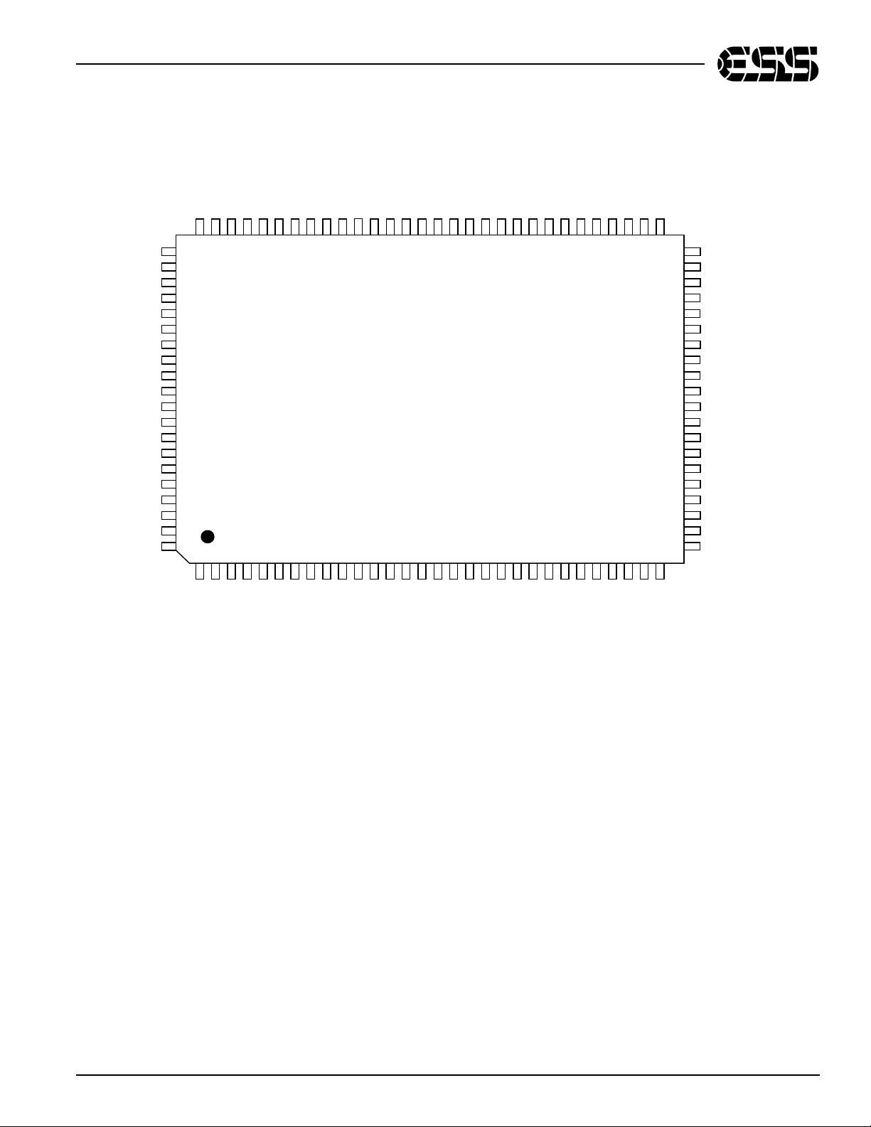
ES4228 PINOUT
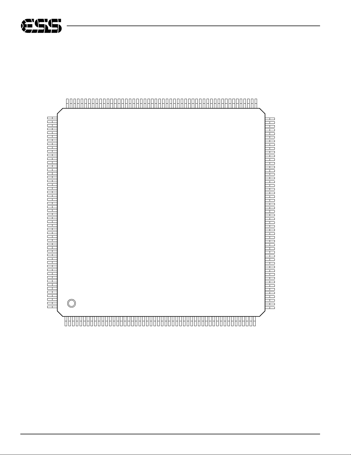
Figure 1 shows the ES4228 device pinout.
NC
NC
VSS
VCC
NC
VPP
AUX0
AUX1
AUX2
VSS
VCC
AUX3
AUX4
AUX5
AUX6
AUX7
LOE#
VSS
VCC
LCS0#
LCS1#
LCS2#
LCS3#
VSS
LD0
LD1
LD2
LD3
LD4
VCC
VSS
LD5
LD6
LD7
LD8
LD9
LD10
LD11
VSS
VCC
LD12
LD13
LD14
LD15
LWRLL#
LWRHL#
VSS
VCC
NC
NC
LA0
LA1
LA2
LA3
VSS
NC
154
155
156
157
158
159
160
161
162
163
164
165
166
167
168
169
170
171
172
173
174
175
176
177
178
179
180
181
182
183
184
185
186
187
188
189
190
191
192
193
194
195
196
197
198
199
200
201
202
203
204
205
206
207
208
1 2 3 4 5 6 7 8 9101112131415161718192021222324252627282930313233343536373839404142434445464748495051
NC
153
NC
152
NC
NC
VCC
VSS
NC
NC
145
146
147
148
149
150
151
HD4
HD5
HD6
NC
144
NCNCHD15
142
143
VSS
HD13
HD12
HD11
HD10
HD9
HD14
VCC
137
138
139
140
141
HD8
HD7
VCC
130
131
132
133
134
135
136
VSS
129
HD3
125
126
127
128
ES4228
208-Pin PQFP Package
HD2
124
HD1
123
HD0
122
VCC
121
VSS
120
HSYNC#
119
VSYNC#
118
PCLKQSCN
117
ES4228/ES4227 PRODUCT BRIEF
PCLK2XSCN
YUV7
YUV6
YUV5
VSS
VCC
YUV4
YUV3
YUV2
YUV1
YUV0
DCLK
105
106
107
108
109
110
111
112
113
114
115
116
52
104
103
102
101
100
99
98
97
96
95
94
93
92
91
90
89
88
87
86
85
84
83
82
81
80
79
78
77
76
75
74
73
72
71
70
69
68
67
66
65
64
63
62
61
60
59
58
57
56
55
54
53
VCC
VSS
DSCK
DQM
DCS0#
VCC
VSS
DCS1#
DB15
DB14
DB13
DB12
VCC
VSS
DB11
DB10
DB9
DB8
DB7
DB6
VSS
VCC
DB5
DB4
DB3
DB2
DB1
DB0
VSS
VCC
DRAS2#
DRAS1#
DRAS0#
DWE#
DOE#/DSCK_EN
DCAS#
VCC
VSS
DMA11
DMA10
DMA9
DMA8
DMA7
DMA6
VSS
VCC
DMA5
DMA4
DMA3
DMA2
DMA1
DMA0
VCC
LA4
LA5
LA6
LA7
LA8
LA9
VSS
VCC
VSS
LA11
LA12
LA13
LA10
VCC
LA14
LA15
LA16
LA17
LA18
LA19
VSS
VCC
LA21
LA20
TDMDR
RESET#
TDMCLK
TDMDX/RSEL
TDMFS
VSS
VCC
TDMTSC#
SEL_PLL2
TSD/SEL_PLL0
TWS/SEL_PLL1
MCLK
NC
VSS
VCC
TBCK
RSD
XIN
VSS
RWS
VCC
XOUT
RBCK
APLLCAP
NC
NC
NC
Figure 1 ES4228 Device Pinout
2 SAM0378-053001 ESS Technology, Inc.
Page 3
ES4228/ES4227 PRODUCT BRIEF
ES4228 PIN DESCRIPTION
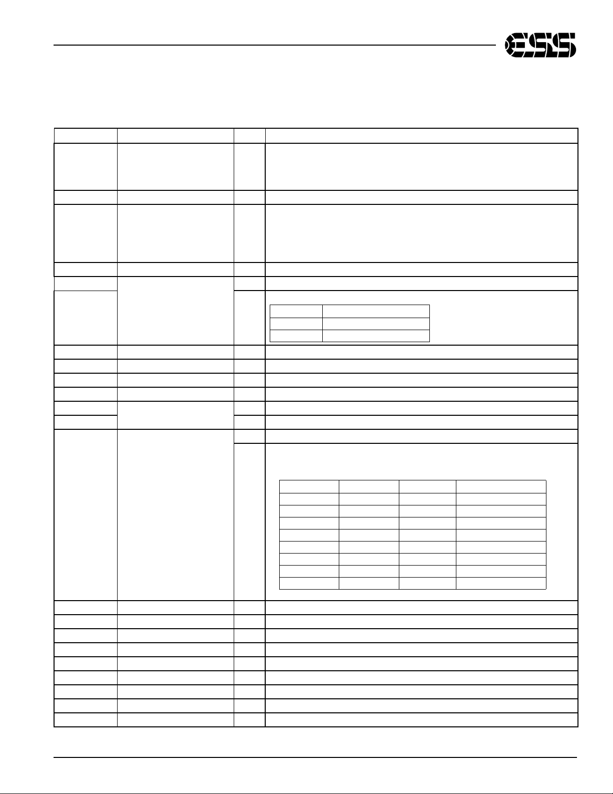
Table 1 lists the pin descriptions for the ES4228.
Table 1 ES4228 Pin Descriptions List
Name Number I/O Description
1, 9, 18, 27, 35, 44 , 5 1, 5 9,
VCC
LA[21:0] 23:19, 16:10, 7:2, 207:204 O Device address output.
VSS
RESET# 24 I Reset input, active low.
TDMDX
RSEL
TDMDR 28 I TDM receive data.
TDMCLK 29 I TDM clock input.
TDMFS 30 I TDM frame sync.
TDMTSC# 31 O TDM output enable, active low.
TWS 32 O Audio transmit frame sync.
SEL_PLL1 I Refer to the description and matrix for SEL_PLL0 pin 33.
TSD
SEL_PLL0
68, 75, 83, 92, 99, 104, 1 1 1 ,
121, 130, 139, 148, 157,
164, 172, 183, 193, 201
8, 17, 26, 34, 43, 52, 60,
67, 76, 84, 91 , 98, 103, 1 12,
120, 129, 138, 147, 156,
163, 171, 177, 184, 192,
200, 208
25
33
I
3.45 V power supply.
I
Ground.
O TDM transmit data.
I ROM Select.
RSEL Selection
0 8-bit ROM
1 16-bit ROM
O Audio transmit serial data port.
I System and DSCK output clock frequency selection at reset time. The matrix
below lists the available clock frequencies and their respecitve PLL bit
settings.
SEL_PLL2 SEL_PLL1 SEL_PLL0 Clock Output
000VCO doesn’t work.
0 0 1 27 MHz
0 1 0 Bypass mode
0 1 1 54 MHz
1 0 0 121.5 MHz
1 0 1 81 MHz
1 1 0 94.5 MHz
1 1 1 108 MHz
SEL_PLL2 36 I Refer to the description and matrix for SEL_PLL0 pin 33.
MCLK 39 I/O Audio master clock for audio DAC.
TBCK 40 I/O Audio transmit bit clock.
RSD 45 I Audio receive serial data.
RWS 46 I Audio receive frame sync.
RBCK 47 I Audio receive bit clock.
APLLCAP 48 I Analog PLL Capacitor.
XIN 49 I Crystal input.
XOUT 50 O Crystal output.
ESS Technology, Inc. SAM0378-053001 3
Page 4
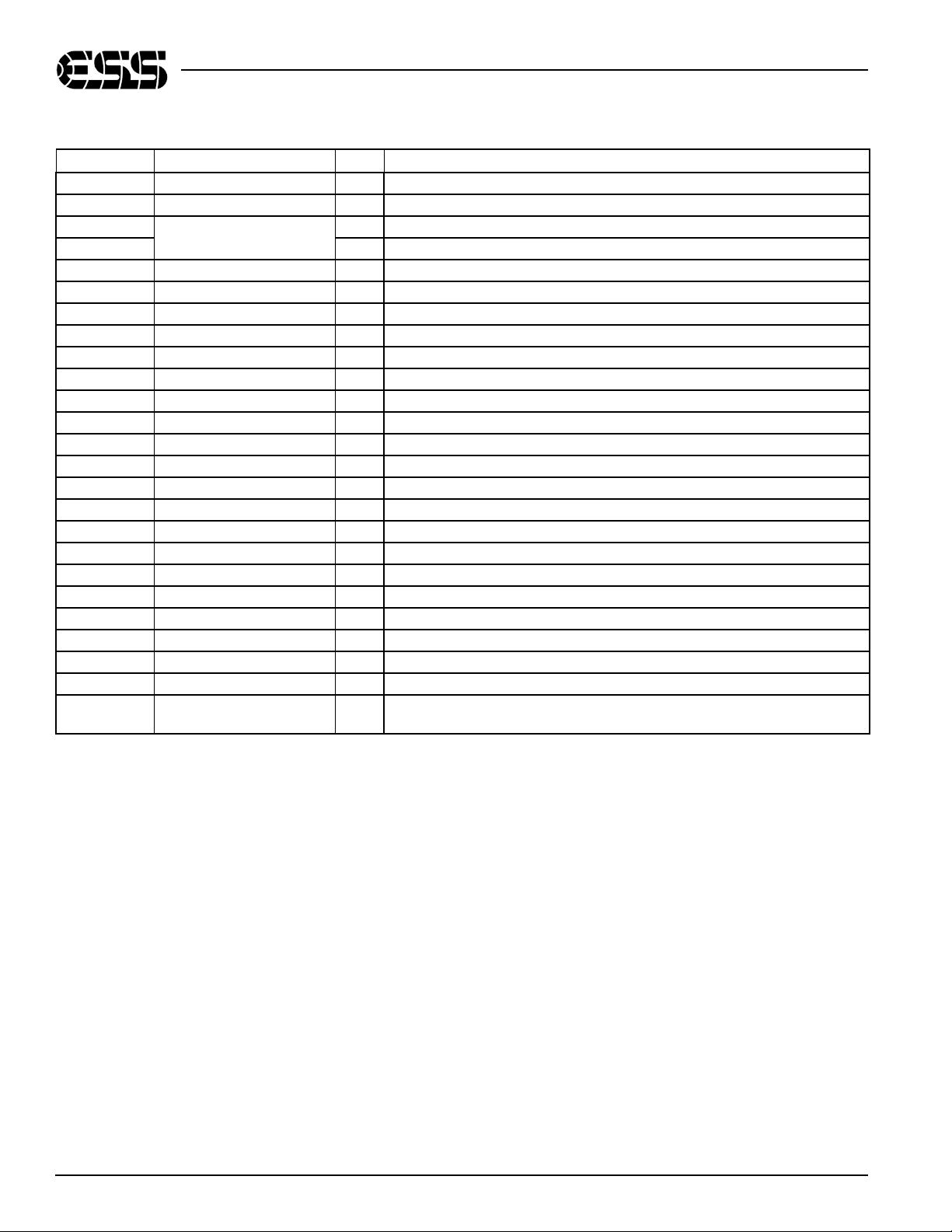
Table 1 ES4228 Pin Descriptions List (Continued)
Name Number I/O Description
DMA[11:0] 66:61, 58:53 O DRAM address bus.
DCAS# 69 O DRAM column address st robe.
DOE# 70 O DRAM output enable.
DSCK_EN O DRAM system clock enable.
DWE# 71 O DRAM write enable.
DRAS[2:0]# 74:72 O DRAM row address strobe.
DB[15:0] 96:93, 90:85 ,82:77 I/O DRAM data bus.
DCS[1:0]# 97, 100 O SDRAM chip select [1:0].
DQM 101 O Data input/output mask.
DSCK 102 O DRAM system clock to SDRAM.
DCLK 105 I Clock input (bypass/test mode).
YUV[7:0] 115:113, 110:106 O 8-bit YUV output.
PCLK2XSCN 116 I/O 2X pixel clock.
PCLKQSCN 1 1 7 I/O Pixel clock.
VSYNC# 118 I/O Vertical sync.
HSYNC# 119 I/O Horizontal sync.
HD[15:0] 141:140, 137:131, 128:122 I/O Host data bus
VPP 159 I 5 V power supply.
AUX[7:0] 169:165, 162:160 I/O Auxiliary ports.
LOE# 170 O EPROM device output enable.
LCS[3:0]# 176:173 O EPROM chip select [3:0].
LD[15:0] 197:194,191:185,182:178 I/O EPROM device data bus.
LWRLL# 198 O EPROM device low byte write enable.
LWRHL# 199 O EPROM device high byte write enable.
NC
37, 38, 41, 42, 146:142,
155:149, 158, 203:202
—
No connect.
ES4228/ES4227 PRODUCT BRIEF
4 SAM0378-053001 ESS Technology, Inc.
Page 5
ES4228/ES4227 PRODUCT BRIEF
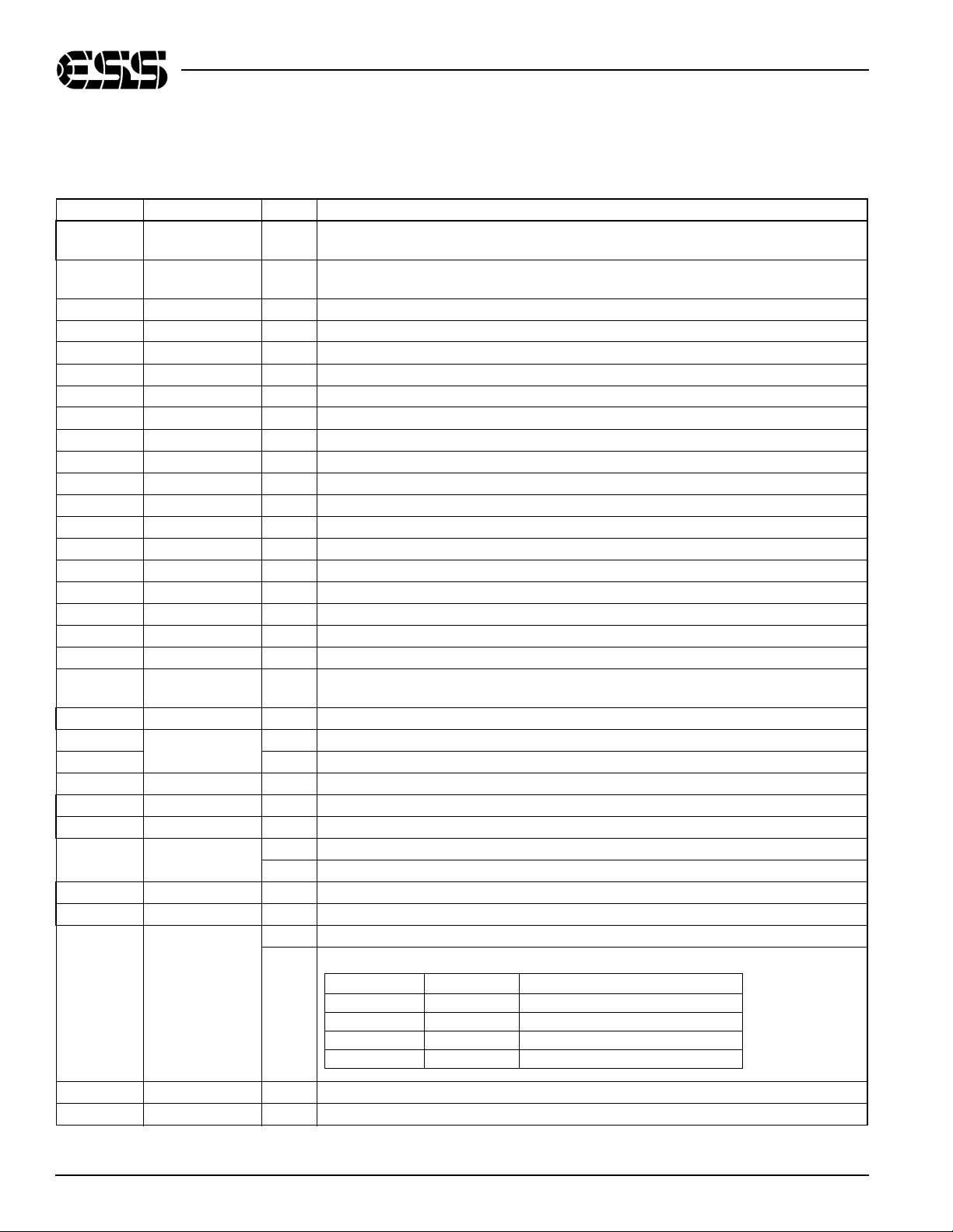
ES4227 PINOUT
Figure 2 shows the ES4227 device pinout.
XIN
VSS
NC
VSS
VCC
PCLK
2XPCLK
VCC
VCCAV
VSSAV
CDAC
VCCAV
RSET
COMP
VSSAV
VSSAA
VREF
VREFM
YDAC
VSSAV
VSSAV
VDAC
ACAP
VCC
AUX6
AUX5
AUX4
AUX3
XOUT
VSS
DSC_D7
HSYNC#
DSC_D6
VSYNC#
DSC_D5
YUV7
YUV6
YUV5
YUV4
VCC
VSS
YUV3
DSC_D4
YUV2
DSC_D3
YUV1
DSC_D2
YUV0
DSC_D1
VSS
80
79 78 77 76 75 74 73 72 71 70 69 68 67 66 65 64 63 62 61 60 59 58 57 56 55 54 53 52
81
82
83
84
85
86
87
88
89
90
91
92
93
94
95
96
97
98
99
100
1
2 3 4 5 6 7 8 9 10111213141516 17181920212223242526272829
NC
NC
NC
VSS
VCC
AUX0
DSC_C
DSC_D0
ES4227
100-pin PQFP
AUX1
AUX2
DSC_S
AUX7
MUTE
RESET#
VCC
AUX8
MCLK
AUX9
TSD
TBCK
RSTOUT#
VSS
VSS
NC
NC
NC
51
30
50
49
48
47
46
45
44
43
42
41
40
39
38
37
36
35
34
33
32
31
NC
MIC1
MIC2
AOL+
AOLAORAOR+
VCCAA
VREFP
VCM
VSSAA
AUX15/IR
AUX14
AUX13
RBCK/SER_IN
AUX12/C2PO
AUX11/IRQ
AUX10
RSD/SEL_PLL0
VCC
VSS
DCLK/EXT_CLK
TWS/SPLL_OUT
Figure 2 ES4227 Device Pinout
RWS/SEL_PLL1
ESS Technology, Inc. SAM0378-053001 5
Page 6
ES4228/ES4227 PRODUCT BRIEF
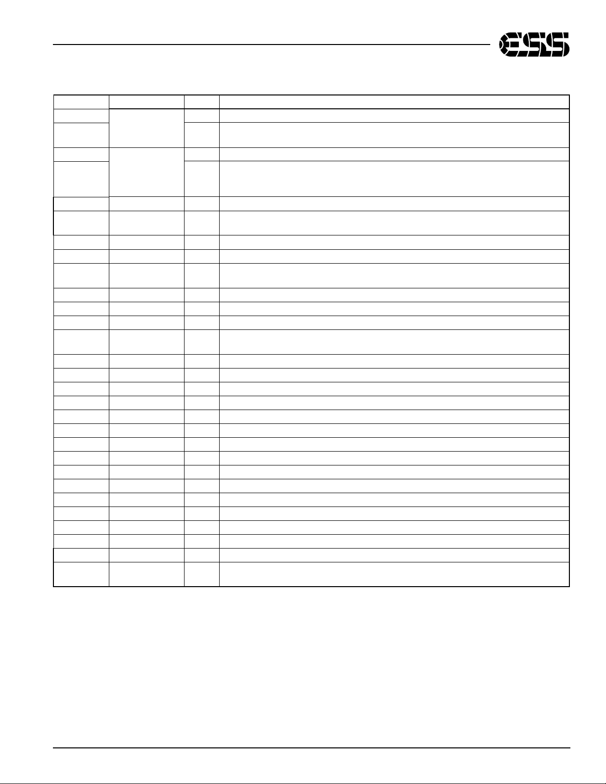
ES4227 PIN DESCRIPTION
Table 2 lists the pin descriptions for the ES4227.
Table 2 ES4227 Pin Descriptions List
Name Number I/O Definition
VSS
VCC
DSC_C 6 I Clock for programming to access internal registers.
AUX0 7 I/O General purpose I/O.
AUX1 9 I/O General purpose I/O.
AUX2 11 I/O General purpose I/O.
AUX3 70 I/O CD loader reset.
AUX4 69 I/O Modem DSP reset.
AUX5 68 I/O General purpose I/O.
AUX6 67 I/O General purpose I/O.
AUX7 14 I/O General purpose I/O.
AUX8 18 I/O General purpose I/O.
AUX9 20 I/O General purpose I/O.
AUX10 34 I/O General purpose I/O.
AUX11 35 I/O Interrupt output to ES4228.
AUX12 36 I/O CD loader C2PO.
AUX13 38 I/O General purpose I/O.
AUX14 39 I/O Interrupt input from Modem DSP.
AUX15 40 I/O IR interrupt Input.
DSC_D[7:0]
DSC_S 10 I Strobe for programming to access internal registers.
DCLK 12 O Dual-purpose pin DCLK is the ES4228 clock.
EXT_CLK I External clock input during bypass PLL mode.
RESET# 13 I Reset.
MUTE 15 O Audio mute.
MCLK 17 I Audio master clock.
TWS 19 I Dual-purpose pin TWS is the transmit audio frame sync.
SPLL_OUT O SPLL_OUT is the select PLL output.
TSD 21 I Transmit audio data input.
TBCK 22 I Transmit audio bit clock.
RWS 23 O Dual-purpose pin RWS is the receive audio frame sync.
SEL_PLL1
1, 25:26, 31, 72,
75, 77, 91, 100
5, 16, 32, 66,
73, 78, 90
8, 81, 83, 85,
93, 95, 97, 99
I
Ground.
I
5.0V power supply.
I/O
Data for programming to access internal registers.
I Pins SEL_PLL[1:0] select the PLL clock frequency for the DCLK output.
SEL_PLL1 SEL_PLL0 DCLK
0 0 Bypas s PLL (input mod e)
0 1 27 MHz (output mode) Default
1 0 32.4 MHz (output mode)
1 1 40.5 MHz (output mode)
RSTOUT# 24 O Reset output (active-low).
NC 2:4,27:30,76 No connect. Do not connect to these pins.
6 SAM0378-053001 ESS Technology, Inc.
Page 7
ES4228/ES4227 PRODUCT BRIEF
Table 2 ES4227 Pin Descriptions List (Continued)
Name Number I/O Definition
RSD
SEL_PLL0
RBCK
SER_IN
VSSAA 41,51 I Audio Analog Ground.
VCM
VREFP 43 I DAC and ADC maximum reference. Bypass to VCMR with 10 µF in parallel with 0.1 µF.
VCCAA 44 I Analog VCC, 5 V.
AOR+,
AORAOL-, AOL+ 47, 48 O Left channel output.
MIC2 49 I Microphone input 2.
MIC1 50 I Microphone input 1.
VREF
VREFM 53 I DAC and ADC minimum reference. Bypass to VCMR with 10 µF in parallel with 0.1 µF.
RSET 54 I Full scale DAC current adjustment.
COMP 55 I Compensation pin.
VSSAV 56:57, 62:63 I Video analog ground
CDAC 58 O Modulated chrominance output.
VCCAV 59, 60 I 5.0V video power supply.
YDAC 61 O Y luminance data bus for screen video port.
VDAC 64 O Composite video output.
ACAP 65 I Audio CAP
XOUT 71 O 27 MHz crystal output.
XIN 74 I 27 MHz crystal input.
PCLK 79 I/O 13.5 MHz pixel clock.
2XPCLK 80 I/O Doubled 27 MHz pixel clock.
HSYNC# 82 O Horizontal sync.
VSYNC# 84 O Vertical sync.
YUV[7:0]
86:89, 92, 94, 96,
33
37
42 I ADC Common Mode Reference (CMR) buffer output. CMR is approximately 2.25 V.
45, 46 O
52 I Internal resistor divider generates Common Mo de R e fere nce (C MR) v oltage. Bypass to
98
O Dual-purpose pin. RSD is the receive audio data input.
I SEL_PLL0 along with SEL_PLL1 select the PLL clock frequency for the DCLK output.
See the table for pin number 23.
O Dual-purpose pin. RBCK is the receive audio bit clock.
I SER_IN is the serial input DSC mode.
0 - Parallel DSC mode.
1 - Serial DSC mode.
Bypass to analog ground with 47 µF electrolytic in parallel with 0.1 µF.
Right channel output.
analog ground with 0.1 µF.
I
YUV data bus for screen video port.
ESS Technology, Inc. SAM0378-053001 7
Page 8
SYSTEM BLOCK DIAGRAM
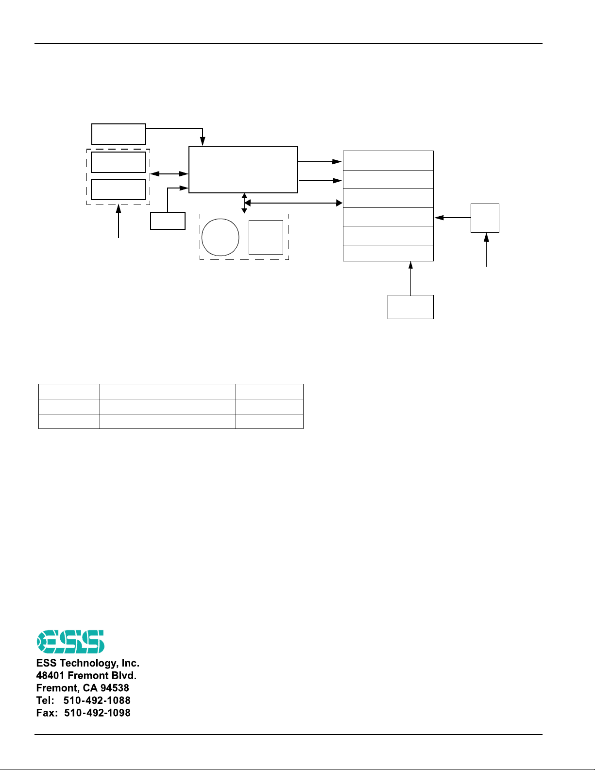
Figure 3 shows the ES4228/ES4227 chipset implemented in a
sample system block diagram.
ES4228/ES4227 PRODUCT BRIEF
ROM or
Flash ROM
ES2898
Modem
ES4228
MPEG Processor
ES2828
MC’97
DAA/Telephone
SDRAM
CD
Loader
Front
Panel /
Keypad
Line Interface
VCD/SVCD Option
Figure 3 ES4228/ES4227 System Block Diagram
ORDERING INFORMATION
Part Number Description Package
ES4228 MPEG Processor 208-pin PQFP
ES4227 Video Encoder Comp an ion Chip 100-pin PQFP
Video
Audio
DSC
ES4227
Companion Chip
Video Encoder
Audio DACs
PLL
Interrupt Port
I/O Expansion
Echo/Surround
Mic
Inputs
IR
Input
Remote
Control
No part of this publication may be reproduced, stored in a
retrieval system, transmitted, or translated in any form or
by any means, electronic, mechanical, ma nual, optical , or
otherwise, without the prior written permission of ESS
Technology, Inc.
ESS Technology, Inc. makes no representations or
warranties regarding the content of this document.
All specifications are subject to change without prior
notice.
ESS Technology, Inc. assumes no responsibility for any
errors contained herein.
(P) U.S. Patent 4,384,169 and others, other patents
pending.
MPEG is the Moving Picture Experts Group of the ISO/
IEC. References to MPEG in this document refer to the
ISO/IEC JTC1 SC29 committee draft ISO 11172 dated
January 9, 1992.
VideoDrive™, SmartScale™, SmartZoom™ and
SmartStream™ are trademarks of ESS Technology, Inc.
Dolby is a trademark of Dolby Laboratories, Inc.
H.261 refers to the International Standard described in
recommendation H.261 of the CCITT Working P arty 15-1.
All other trademarks are trademarks of their respective
companies and are used for identification purposes only.
All other trademarks are owned by their respective
holders and are used for identification purposes only.
8 © 2000—2001 ESS Technology, Inc. All rights reserved. SAM0378-053001
 Loading...