

Page 1
ES3880
Video CD MPEG Processor
Product Brief
DESCRIPTION
The ES3880 Video CD MPEG processor is ESS’ third
generation highly integrated, optimal quality, and costeffective single chip solution for Video CD players. The
ES3880 is the best quality available for both video and
audio and easily pass es the highest graded leve l for the
China VCD standard
video and audio processing and a full-fledged MPEG
system bit stream pars er. The ES3880 can be use d as a
microcontroller to provide system control, while also
performing such basic video operations as arbitrary
scaling and video filtering. The MPEG-1 system layer
bitstream is decoded at up to 9 Mb/s at Standard
Intermediate Format (SIF) resolution with a picture rate of
30 frames per seco nd. Two channels of MPEG -1 Laye r 1
or Layer 2 audio are decoded simultaneously.
The ES3880 supports SmartScale advanced scaling
techniques, along wi th SmartStream for audio and video
error concealment, and SmartZoom for enabling in/out
zooming of a particular area of a still picture or movie.
Additional features include DiscScan, TrackScan, QuickScan, OnScreen-Display (OSD), Karaoke, Playback Control (PBC)
for Video CD 2.0, and entertainment game software.
System control and house-keeping functions (keypad and
remote control) are also provided.
The ES3880 can be implem ented wi th the E S3883 Video
CD Video Encoder, which integrates most of the analog
discrete components required for a Video CD player.
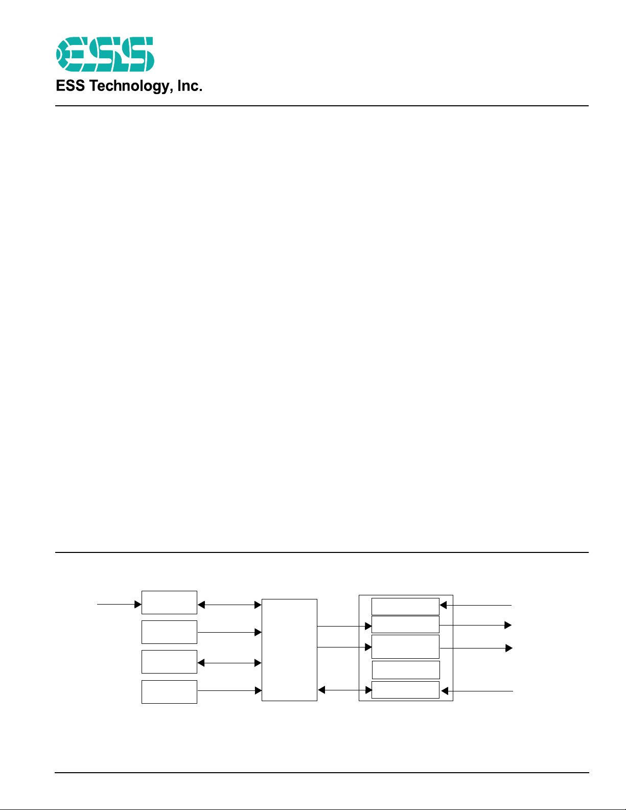
Figure 1 shows a typical Video CD system using the
ES3880 and the companion ES3883 video encoder. When
the ES3880 and ES3883 are used in the design,
enhanced support for 3DSound and SurroundSound is
realized, along with support for interactive games.
.
The ES3880 integrates MPEG-1
The ES3880 is available in an industry-standard 100-pin
Plastic Quad Flat Pack (PQFP) package.
FEATURES
• Programmable Multimedia Processor (PMP) architecture
• MPEG-1 aud i o/ video decoder and system parser
• CD block decoder functions
• Video interlacing hardware
• Color Space Conversion (CSC)
• STC interpretation and video/audio Phase-lock Loop (PLL)
• Supports both 8- and 16-bit YUV output
• 256/384 frame sampling frequency for audio system clock
• Programmable master clock for external audio DAC
• Independent bit clock for audio transmit and receive
• SmartScale video scaling supports X- and Y-axis interpolation
• SmartZoom supports 4X picture enlargement and reduction
• SmartStream supports audio and video bit stream error
concealmen t
• SmartVocal: cancels the vocal on an audio-CD
• Karaoke function
• Video Fader for fading video image (in and out)
• On-screen-Display (OSD)
• Playback Control (PBC) for Video CD 2.0
• Trick mode functions (Repeat, Goto, Set A-B, etc.)
• DiscScan, TrackScan, and QuickScan
• Video CD 1.1 and 2.0, and Audio CD compatible
• Power management
• 3.6 V power supply with 5 V tolerant I/O’s
• 100-pin PQFP
• Can be used with either serial or parallel interfaces
ES3883 Video CD
Compani on Chi p
Keypad
ESS Technology, Inc. SAM0191-052901 1
Panel
Interface
CD-ROM
DRAM
256K X 16
ROM
Echo
Audio
ES3880
Video CD
MPEG
Processor
Figure 1 ES3880 System Block Diagram
Video
DSC
Audio DAC
NTSC/PAL
Encoder
Interrupt
I/O Expansion
Microphone
Speakers
Television
IR
Page 2
ES3880 PINOUT
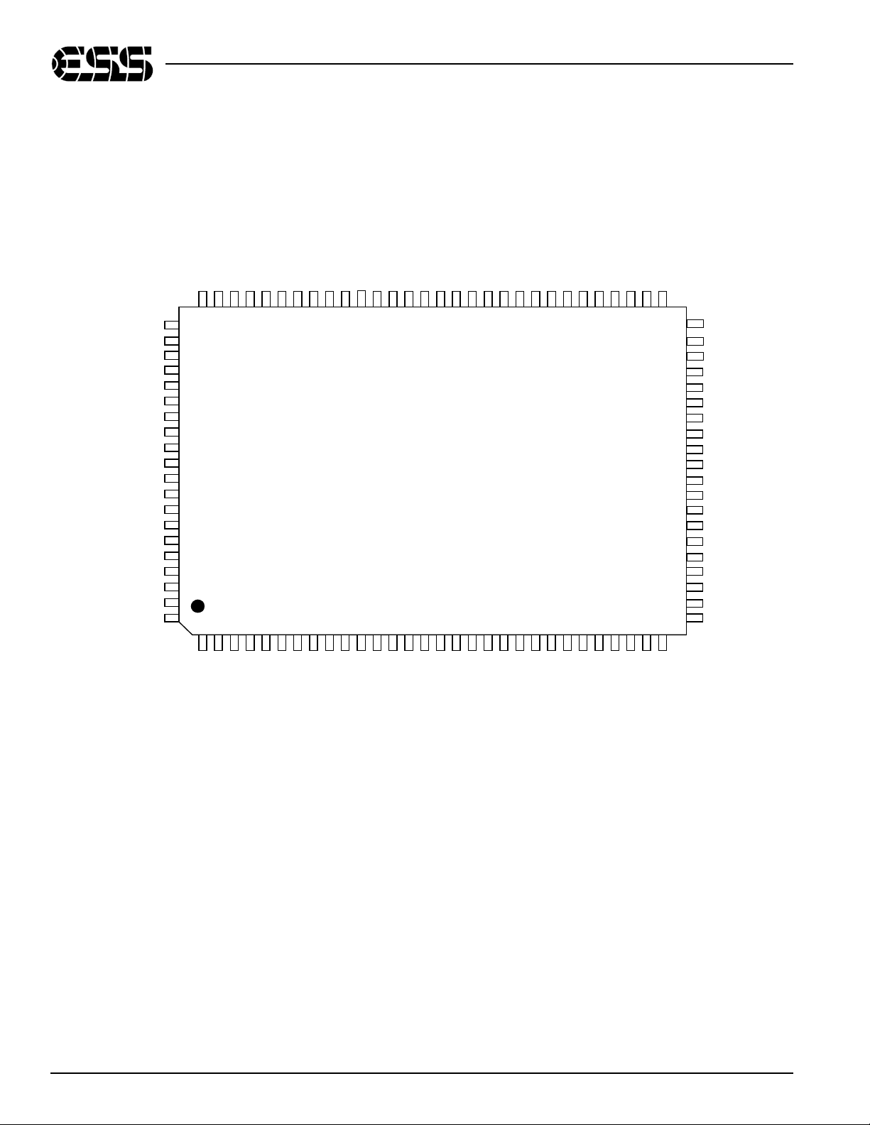
Figure 2 shows the ES3880 device pinout.
ES3880 PRODUCT BRIEF
ES3880 PINOUT
VPP
LA12
LA13
LA14
LA15
LA16
LA17
ACLK
AOUT/SEL_PLL0
ATCLK
ATFS/SEL_PLL1
DA9/DOE#
AIN
ARCLK
ARFS
TDMCLK
TDMDR
TDMFS
CAS#
VSS
LA11
LA10
VSS
80
79 78 77 76 75 74 73 72 71 70 69 68 67 66 65 64 63 62 61 60 59 58 57 56 55 54 53 52
81
82
83
84
85
86
87
88
89
90
91
92
93
94
95
96
97
98
99
100
1
2 3 4 5 6 7 8 9 10 11 12 13 14 15 16 17 18 19 20 21 22 23 24 25 26 27 28 29
VDD
RAS#
DWE#
LA9
DA0
LA8
DA1
LA7
DA2
LA6
DA3
LA5
DA4
LA4
DA5
LA3
LA2
LA1
LA0
LCS0#
LCS1#
LOE#
LCS3#
LWR#
ES3880
100-pin PQFP
DA6
DA8
DA7
DBUS0
DBUS1
DBUS2
DBUS3
DBUS4
DBUS5
LD7
DBUS6
LD6
DBUS7
LD5
DBUS8
LD4
DBUS9
LD3
DBUS10
LD2
DBUS11
LD1
DBUS12
LD0
DBUS13
AUX7
DBUS14
VDD
AUX5
AUX6
51
50
VSS
AUX4
49
AUX3
48
AUX2
47
AUX1
46
AUX0
45
PCLK
44
PCLK2X
43
CPUCLK
42
HSYNC
41
VSYNC
40
YUV7
39
YUV6
38
YUV5
37
YUV4
36
YUV3
35
YUV2
34
YUV1
33
YUV0
32
31
30
DBUS15
RESET#
VDD
VSS
Figure 2 ES3880 Device Pinout
2 SAM0191-052901 ESS Technology, Inc.
Page 3
ES3880 PRODUCT BRIEF
PIN DESCRIPTION
PIN DESCRIPTION
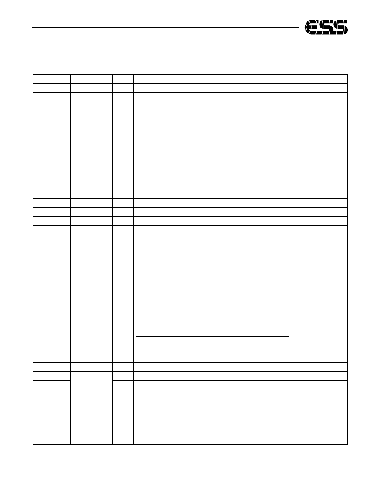
Table 1 lists the pin descriptions for the ES3880.
Table 1 ES3880 Pin Descriptions List
Name Number I/O Definition
VDD 1, 31, 51 I 3.3V power supply.
RAS# 2 O Row address strobe.
DWE# 3 O DRAM write enable.
DA[8:0] 12:4 O DRAM multiplexed row and column address bus.
DBUS[15:0] 28:13 I/O DRAM data bus.
RESET# 29 I System reset.
VSS 30, 50, 80, 100 I Ground.
YUV[7:0] 39:32 O YUV[7:0] 8-bit video data bus.
VSYNC 40 I/O Vertical sync.
HSYNC 41 I/O Horizontal sync.
CPUCLK 42 I RISC and system clock input. CPUCLK is used only if SEL_PLL[1:0] = 00 to bypass
PLL.
PCLK2X 43 I/O Doubled 54 MHz pixel clock.
PCLK 44 I/O 27 MHz pixel clock.
AUX[7:0] 54:52, 49:45 I/O Auxiliary control pins 7:0. AUX0 and AUX1 are open collectors.
LD[7:0] 62:55 I/O RISC interface data bus.
L WR# 63 O RISC interface write enable.
LOE# 64 O RISC interface output enable.
LCS[3,1, 0]# 65, 66, 67 O RISC interface chip select.
LA[17:0] 87:82, 79:68 O RISC interface address bus.
VPP 81 I 5.0V power supply.
ACLK 88 I/O Master clock for external audio DAC.
AOUT
O Audio interface serial data output when selected.
I System and DSCK output clock fr equency sele ction at reset time. The matrix below lists
the available clock frequencies and their respective PLL bit settings.
SEL_PLL0
ATCLK 90 I/O Audio transmit bit clock.
ATFS
SEL_PLL1 I Refer to the description and matrix for SEL_PLL0 pin 89.
DA9 92 O DRAM multiplexed row and column address line 9.
DOE# O DRAM output enable.
AIN 93 I Audio serial data input.
ARCLK 94 I Audio receive bit clock .
ARFS 95 I Audio receive frame sync.
TDMCLK 96 I TDM serial clock.
ESS Technology, Inc. SAM0191-052901 3
89
91
SEL_PLL1 SEL_PLL0 DCLK
0 0 Bypass PLL (input mode)
0 1 54 MHz (output mode) Def ault
1 0 67.5 MHz (output mode)
1 1 81.0 MHz (output mode)
O Audio transmit frame sync.
Page 4
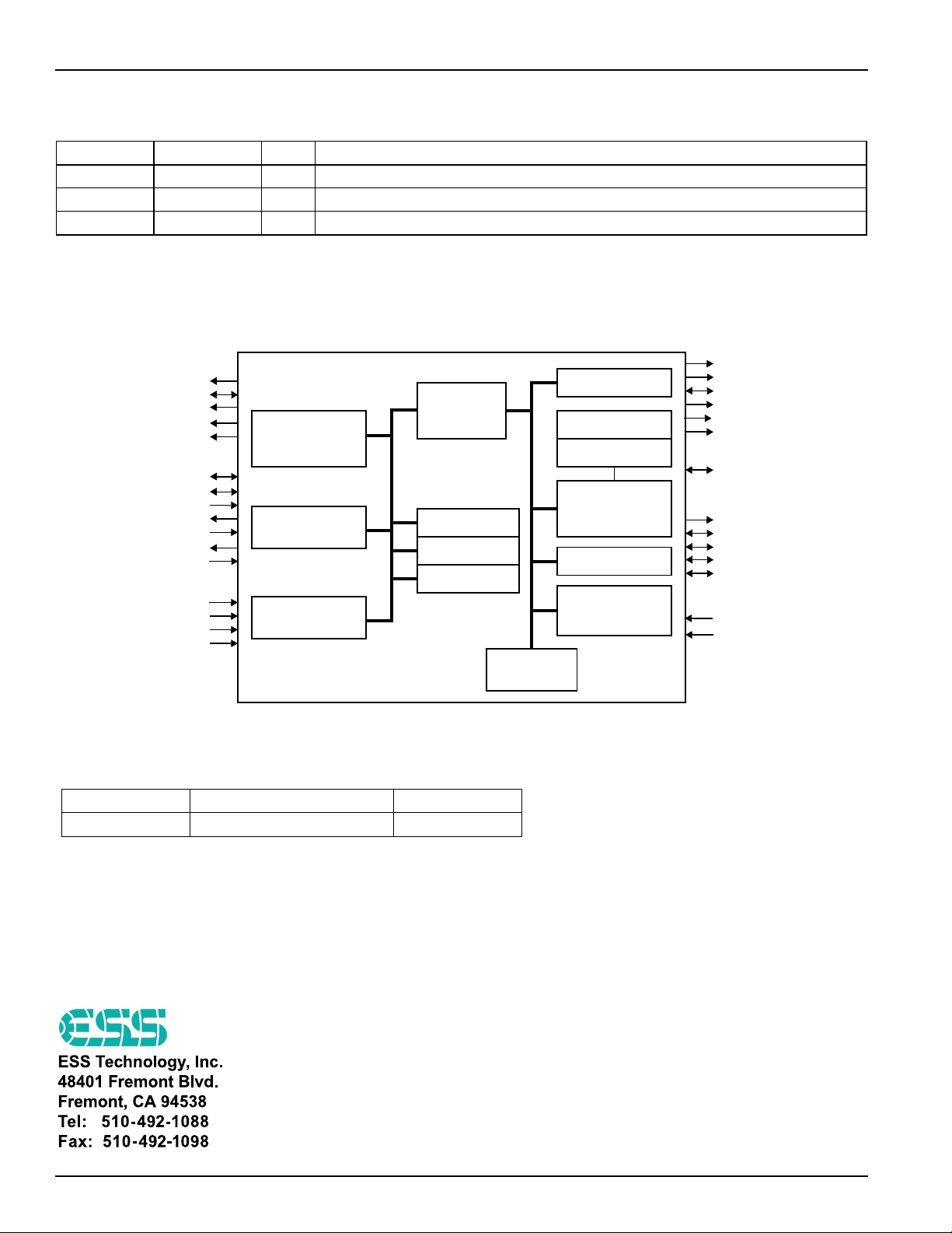
Table 1 ES3880 Pin Descriptions List (Continued)
Name Number I/O Definition
TDMDR 97 I TDM serial data receive.
TDMFS 98 I TDM frame sync.
CAS# 99 O DRAM column address strobe.
BLOCK DIAGRAM
Figure 3 provides a functional block diagram of the
ES3880.
ES3880 PRODUCT BRIEF
BLOCK DIAGRAM
Processor
Interface
LCS3#, LCS#[1:0]
Serial
Audio
Interface
LA[17:0]
LD[7:0]
LWR#
LOE#
ACLK
ATCLK
AIN
AOUT
ARFS
ATFS
ARCLK
RISC
Processor
Serial Audio
Interface
Huffman
Decoder
64x32 ROM
32x32 SRAM
Registers
TDM
Interface
SEL_PLL[1:0]
TDMCLK
TDMDR
TDMFS
TDM
Interface
Figure 3 ES3880 Functional Block Diagram
ORDERING INFORMATION
Part Number Description Package
ES3880 Video CD MPEG Processor 100-pin PQFP
DR A M Interface
DRAM DMA
Controller
2Kx32 ROM
512x32 SRAM
MPEG
Processor
Video Output
On Screen
Display
RAS#
DA[9:0]
DBUS[15:0]
DOE#
DWE#
CAS#
AUX[7:0]
YUV[7:0]
PCLK2X
PCLK
VSYNC
HSYNC
CPUCLK
RESET#
DRAM
AUX
Screen
Display
Misc.
No part of this publication may be reproduced, stored in a
retrieval system, transmitted, or translated in any form or
by any means, electronic, mechanical, ma nual, optical , or
otherwise, without the prior written permission of ESS
Technology, Inc.
ESS Technology, Inc. makes no representations or
warranties regarding the content of this document.
All specifications are subject to change without prior
notice.
ESS Technology, Inc. assumes no responsibility for any
errors contained herein.
(P) U.S. Patent 4,384,169 and others, other patents
pending.
SmartScale™, SmartStream™, and VideoDrive™ are
trademarks of ESS Technology, Inc.
MPEG is the Moving Picture Experts Group of the ISO/
IEC. References to MPEG2 in this document refer to the
ISO/IEC 13818-1.
All other trademarks are owned by their respective
holders and are used for identification purposes only.
4 © 2000 ESS Technology, Inc. All rights reserved. SAM0191-052901
 Loading...