

Page 1
ES2898/ES2828
V.90 PCI DSP Modem Solution
ESS Technology, Inc.
DESCRIPTION
The ESS Technology ES2898/ES2828 TeleDrive® chipset
is a highly integrated solution that brings advanced
modem functionality to notebooks, desktops, and add-incards. The ES2898/ES2828 chipset provides an efficient
56k (V.90) data/fax solution and adds both a telephone
answering machine (TAM) feature and a full-duplex
speakerphone feature.
The data pump algorithms run on the ES2898 DSP, along
with the echo cancellation required for implementing a fullduplex speakerphone feature. The host CPU is utilized to
run the modem controller functions, including the standard
AT command set, V.42bis data compression features,
Classes 1 and 2 fax, and ITU-T V.80 sync access to
support H.324 video conferencing applications. The
ES2898 DSP offers an integrated PCI bus interface.
The ES2828 is the companion analog-front-end (AFE)
chip to the ES2898. It integrates a low-pass, continuoustime anti-aliasing filter, a 16-bit resolution ADC, a 16-bit
DAC, a low-pass output-reconstruction filter, and a CHI
bus interface to interface to the ES2898. The ES2828
includes two signal processing channels that operate
synchronously so that data reception at the ADC channel
and data transmission from the DAC channel occur during
the same time interval. The ES2828 also incorporates an
AC-Link to interface to core logic chipsets to provide a
standalone MC‘97 host-based V.90/V.92 modem solution.
The ES2898 DSP is available in an industry-standard 100pin low-profile quad flat pack (LQFP) package. The
ES2828 is available in an industry-standard 48-pin lowprofile quad flat pack (LQFP) package.
Product Brief
MODEM FEATURES
• Data mode capabilities:
—– V.90 56 kbps
—– V.34 33.6 kbps and fallbacks
—– Standard AT command set
—– V.42 (LAPM) and MNP error correction
—– V.42bis/MNP 5 data compression
—– 3.3V power supply, 5V input tolerant
• Fax mode capabilities:
—– ITU-T V.17, V.21 ch2, V.27ter, and V.29
—– Group 3 (TIA/EIA 578 Class 1 and Class 2)
• Telephony capabilities:
—– Telephone answering machine
—– Full duplex speakerphone
—– Caller ID
• Sigma-delta modulation codec
• Programmable downsampling frequency for modem and
voice applications
• ACPI power management support
• TIES escape sequence
• V.80 (H.324 software stack compatible)
• Fully ACPI-compliant
• Microsoft Windows 98/SE/ME/2000:
—– UNIMODEM V
—– TAPI
• Microsoft Windows NT 4.0
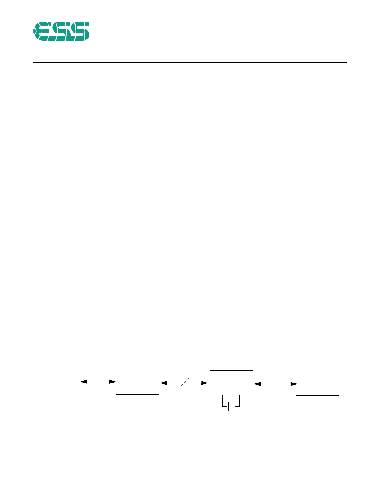
SYSTEM BLOCK DIAGRAM
Figure 1 Shows the ES2898/ES2828 system block
diagram.
CHI BUS I/F
PCI BUS
INTERFACE
ESS Technology, Inc. SAM0402-050301 1
ES2898
TeleDrive
Figure 1 ES2898/ES2828 System Block Diagram
4
ES2828
Modem AFE
DAA
18.816 MHz
Page 2
PINOUT
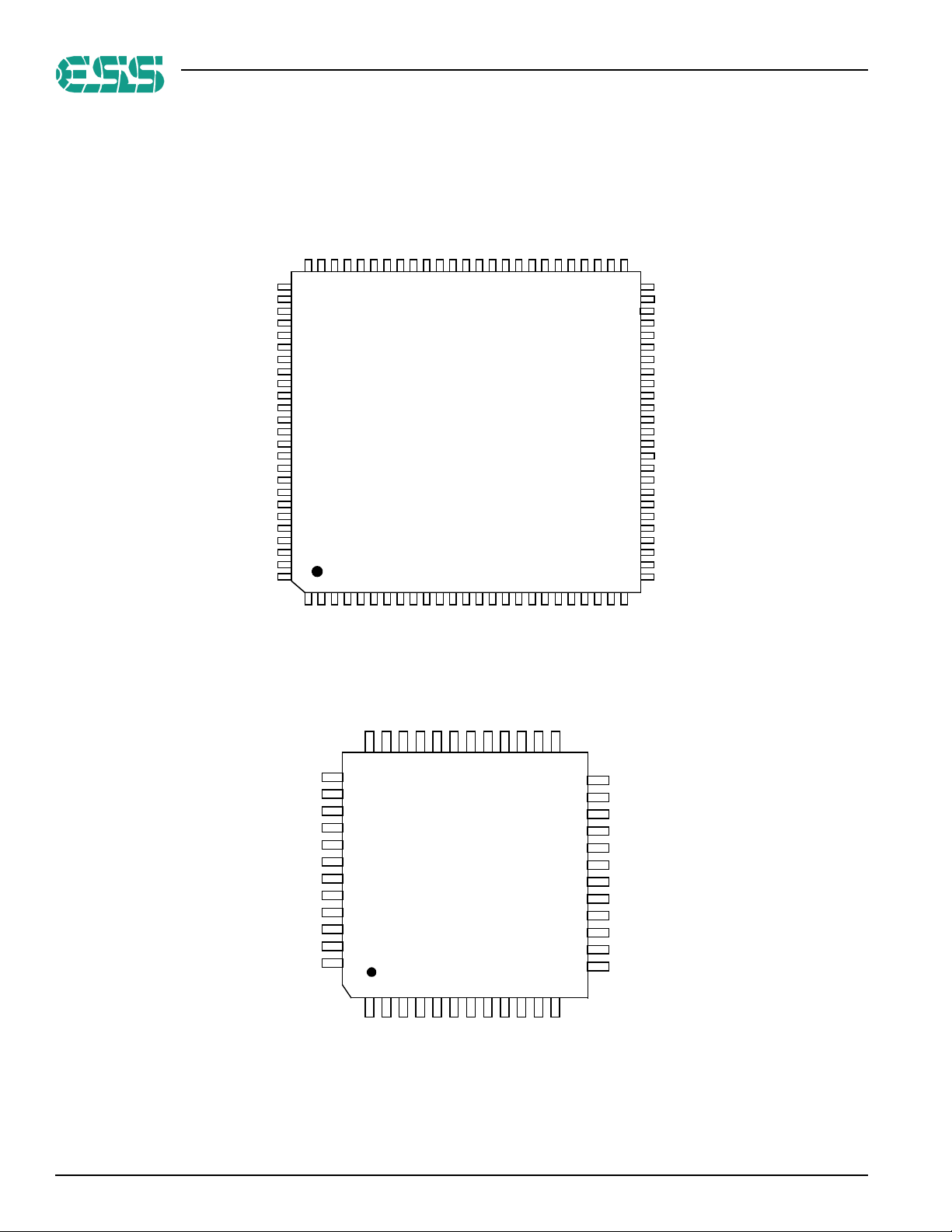
Figure 2 shows the ES2898 and ES2828 pinout diagrams.
SCLK1
RFS1
TFS1
DR1
DT1
GND
SCLK0
RFS0
TFS0
DR0
75747372717069686766656463626160595857565554535251
DT0
VDD
TEST/PF9
RING_IN
VAUX
PME#
VAUXP
VDD
PCI CLK
VDD
INTA
PAR
RST#
FRAME#
GND
IRDY#
STOP#
VDD
DAA_PM
TRDY#
IDSEL
DEVSEL#
AD31
AD30
AD29
76
77
78
79
80
81
82
83
84
85
86
87
88
89
90
91
92
93
94
95
96
97
98
99
100
1
2345678
ES2898S
100-Pin LQFP
9
101112131415161718192021222324
ES2898/ES2828 PRODUCT BRIEF
PINOUT
BSEL0
SEDO
NC
NC
NC
PF7
VDD(5V)
PF3
PF4
PF5
PF6
FL2
PF0
PF1
PF2
50
FL1
49
FL0
48
VDD
47
GND
46
VDD
45
BSEL1
44
CLKOUT
43
XTALO
42
XTALI
41
GND
40
AD0
39
AD1
38
AD2
37
AD3
36
AD4
35
AD5
34
AD6
33
AD7
32
CBE0#
31
CBE1#
30
AD8
29
AD9
28
AD10
27
AD11
26
AD12
25
VAUX
GPIO_0
GPIO_1
GPIO_2
GPIO_3
GPIO_4
GPIO_5
DGND
GPIO_6
GPIO_7
GPIO_8
GPIO_9
NC
VDD
VDD
AD28
S D ATA_I N
ID0
P W DN#
ID1
RST#
36 35 34 33 32 31 30 29 27 2628
37
38
39
40
41
42
43
44
45
46
47
48
1
ES2828S
48-PIN LQFP
2 3 4 5 6 7 8 9 10 11 12
DPBX
DVDD
A G ND
A G ND
CBE3#
X T ALI
X T ALO
DVDD
CKOFSS C
A U X-
AUX+
A G ND
RXIN+
VDD
GND
AD16
AD17
AD18
AD19
AD20
AD21
AD22
AD23
AD24
AD25
AD26
AD27
GND
GND
AD13
AD14
AD15
CBE2#
S O
25
24
SI
23
DVDD
22
CTST
DGND
21
20
HCT
VCMX
19
18
AGND
17
TX-
16
TX+
VRBP
15
VREF
14
VCBP
13
V C M
A V DD
RXIN-
A C LIN K/ GPIO_ B
Figure 2 ES2898 and ES2828 Pinout Diagrams
2 SAM0402-050301 ESS Technology, Inc.
Page 3
ES2898/ES2828 PRODUCT BRIEF
PIN DESCRIPTIONS
PIN DESCRIPTIONS
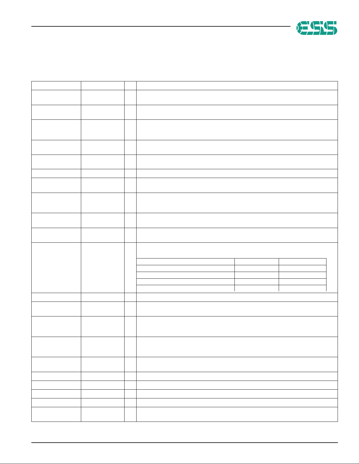
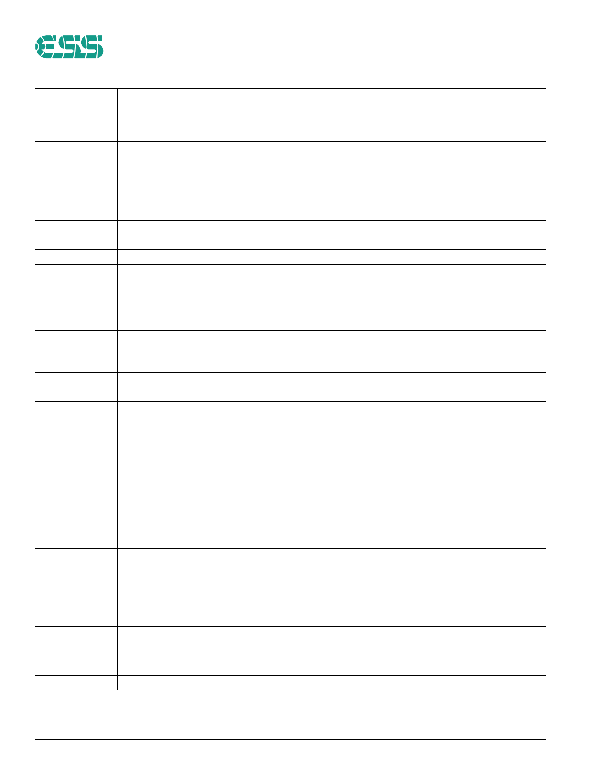
Table 1 lists the ES2898 pin descriptions. Table 2 lists the
ES2828 pin descriptions.
Table 1 ES2898 Pin Descriptions
Names Pin Numbers I/O Definitions
AD[16:31]
GND 14, 20, 22, 41, 47,
C/BE[3:0]#
VDD 16, 18, 46, 48, 77,
VDD
PERR# 19 O Parity error output.
AD[0:15]
XTALI 42 I ES2898 clock input. This pin can be driven by either a crystal or an oscillator. When using a
XTALO 43 O Works in conjunction with XTALI when a crystal is used. When an oscillator is used, XTALO is
CLKOUT 44 O Fixed-frequency clock output. The frequency of this pin is the same as the crystal input of the
BSEL1 / BSEL0 45, 61 I Used to determine the operating mode of the ES2898. These pins are sampled at the falling
FL0 49 O Used as flag 0 output during normal operation.
FL1 50 O Used as flag 1 output during normal operation while the bypass circuitry is included. Will be
FL2 51 O Functions as flag 2 output during normal operation, and can also be used to provide a pass-
PF[7:0] 52, 53, 54, 55, 56,
VDD(5V) 60 I Digital supply voltage. If the ES2898 interfaces with a 5V input, tie this pin to 5V. Otherwise, tie
SEDO 62 I Serial EEPROM data input.
SECS 63 O Serial EEPROM chip select.
SEDI 64 O Serial EEPROM serial data output.
SECLK 65 O Serial EEPROM clock.
SCLK1 66 I/O One of two serial clock inputs. This clock can be generated either by the ES2898 or by the
1:13, 98, 99, 100 I
71, 90
15, 21, 31, 32 I
83, 85, 93
17 I
23:30, 33:40 I/O
57, 58, 59
When the ES2898 interfaces a PCI bus, these pins function as AD[16:31]. The PCI bus
implements a 32-bit multiplexed address and data bus.
— Ground.
Bus command/byte enable. These pins are multiplexed. During the address phase of a bus
transaction, these pins define the bus command. During the data phase, these pins are used as
byte enables.
I Digital supply voltage, 3.3V.
When the ES2898 interfaces a PCI bus, use an internal chip select and tie the CS pin to this
VDD pin through a pullup 10k Ω resistor.
When the ES2898 interfaces a PCI bus, these pins function as AD[15:0]. The PCI bus
implements a 32-bit multiplexed address and data bus.
crystal, XTALO is used as the other crystal pin. When using an oscillator, the output of the
oscillator is connected to XTALI. An internal clock doubler doubles the frequency at XTALI.
left unconnected.
DSP clock. The clock is stopped during D2 and D3 states when the ST_CLKOUT bit is set.
edge of reset and are encoded as follows:.
Configuration BSEL1 (pin 45) BSEL0 (pin 61)
Reserved 0 0
Reserved 0 1
PCI interface 1 0
Generic 16-bit host interface 1 1
activated during power-down mode.
through reset to the ES2828. To bring the devices out of reset, write a logic zero. FL2 carries
the reset signal for the ES2828.
I/O General-purpose programmable bidirectional flag pins. These pins can be used for interfacing
with a telephone or other device, performing such functions as phone-off-hook, phone-on-hook,
ring, caller ID, etc. PF[0] is specially designed to support the ring function.
this pin to 3.3V.
ES2828.
ESS Technology, Inc. SAM0402-050301 3
Page 4
ES2898/ES2828 PRODUCT BRIEF
PIN DESCRIPTIONS
Table 1 ES2898 Pin Descriptions (Continued)
Names Pin Numbers I/O Definitions
RFS1 67 I/O Receive frame for serial port 1. Can be generated either internally or externally. This signal is
TFS1 68 I/O Transmit frame for serial port 1. Can be generated either internally or externally.
DR1 69 I Data receive pin for serial port 1.
DT1 70 O Data transmit pin for serial port 1.
SCLK0 72 I/O One of two serial clock inputs. This clock can be generated either by the ES2898 or by the
RFS0 73 I/O Receive frame for serial port 0. Can be generated either internally or externally. This signal is
TFS0 74 I/O Transmit frame for serial port 0. Can be generated either internally or externally.
DR0 75 I Data receive pin for serial port 0.
DT0 76 O Data transmit pin for serial port 0.
TEST / PF9 78 I Used during device test. Tie this pin to ground through a 4.7k Ω resistor.
RING_IN 79 I Used for ring detect input during the D3
V
AUX
80 I Power to device during implementation of the D3
PME# 81 O PME# output.
VAUXP
82 I
CLK 84 I PCI bus input clock. Functions as PCI CLK pin and operates at 33 MHz.
INTA# 86 O Interrupt A. Used to request an interrupt from the PCI bus.
PAR 87 I/O Parity pin. PAR is stable and valid one clock after the address phase. For data phases, PAR is
FRAME# 89 I/O Cycle frame. FRAME# is driven by the current master to indicate the beginning and duration of
IRDY# 91 I/O Initiator ready. IRDY# is used in conjuction with TRDY# and indicates the bus master’s ability to
STOP# 92 I/O Stop. STOP# indicates the current target is requesting the master to stop the current
TRDY# 95 O Target ready. TRDY# is used in conjuction with IRDY# and indicates the bus master’s ability to
IDSEL 96 O Initialization device select. IDSEL is used as a chip select during configuration read and write
DEVSEL# 97 O Device select. When actively driven, DEVSEL# indicates that the driving device has decoded its
RESET# 88 I Active-low ES2898 reset input.
DAA_PM 94 O DAA power control output.
asserted one clock before data is sent on the DR1 pin.
ES2828.
asserted one clock before data is sent on the DR0 pin.
state to drive the device back to its default power-up
cold
state.
state required by PCI Power Management
cold
Interface specification.
V
support detection input. V
AUX
D3
state. No support when driven low.
cold
pin is driven high to indicate that ACPI is supported with
AUXP
stable and valid one clock after either IRDY# is asserted on a write transaction or TRDY# is
asserted on a read transaction.
an access. FRAME# is asserted to indicate the start of a bus transaction. When FRAME# is
deasserted, the transaction is in the final data phase or has been completed.
complete the current data phase of a transaction. During a write transaction, IRDY# indicates
that valid data is present on AD[16:31] and AD[0:15]. During a read transaction, IRDY#
indicates that master is prepared to accept data. Wait cycles are inserted until both IRDY# and
TRDY# are asserted together.
transaction.
complete the current data phase of a transaction. During a write transaction, TRDY# indicates
that valid data is present on AD[16:31] and AD[0:15]. During a read transaction, TRDY#
indicates that master is prepared to accept data. Wait cycles are inserted until both TRDY# and
IRDY# are asserted together.
transactions.
address as the target of the current access. As an input, DEVSEL# indicates whether any
device on the bus has been selected.
4 SAM0402-050301 ESS Technology, Inc.
Page 5
ES2898/ES2828 PRODUCT BRIEF
Table 2 ES2828 Pin Descriptions
Names Pin Numbers I/O Definitions
DPBX 1 I Digital PBX detection.
ACLINK/GPIO_B 2 I/O Default for CHI bus mode (internal pulldown). Pull high for AC-Link mode.
DVDD 3, 23, 29 P 3.3V digital power.
AGND 4:6, 18 I Analog ground.
AUX+ 7 I Codec analog auxiliary differential positive input. The DC level is Vcm, and the full-scale input is
either 0.22 Vp-p ±5% or 1.1 Vp-p±5%, depending on the gain setting.
AUX- 8 I Codec analog auxiliary differential negative input. The DC level is Vcm, and the full-scale input is
either 0.22 Vp-p ±5% or 1.1 Vp-p±5%, depending on the gain setting.
RXIN+ 9 I Codec analog differential positive input. The DC level is Vcm, and the full-scale input is either 0.22
Vp-p ±5% or 1.1 Vp-p±5%, depending on the gain setting.
RXIN- 10 I Codec analog differential negative input. The DC level is Vcm, and the full-scale input is either
0.22 Vp-p ±5% or 1.1 Vp-p±5%, depending on the gain setting.
AVDD 11 I Analog 5.0V supply.
VCM 12 O Common mode voltage bypass 1. Has a range of 2.16V±5%. Bypass to VCBP with 0.1-µF
VCBP 13 I Ground pin for VCM.
VREF 14 O Voltage reference bypass. Has a range of 1.2356V±5%. Bypass to VRBP with 0.1-µF ceramic
VRBP 15 I Ground pin for VREF.
TX+ 16 O Codec positive analog output. The DC level is Vcm, and the full-scale ac output is either 2.8V
TX- 17 O Codec negative analog output. The DC level is Vcm, and the full-scale ac output is either 2.8V
VCMX 19 O Codec common mode reference voltage output. 2.16V±5%, maximum current ±500 µA, maximum
HCT 20 I Codec digital input mode control.
DGND 21, 44 P Digital ground.
CTST 22 I Codec sigma delta modulator test port output enable.
SI 24 I Serial port input (default).
SO 25 O Serial port output without V
SC 26 I/O Serial port clock output. While input must be TTL-compatible, should be able to handle 3.3V input.
ceramic chip capacitor parallel with 10-µF tantalum capacitor.
chip capacitor parallel with 10-µF tantalum capacitor.
p-p±5% or 1.4V p-p±5%, depending on the gain setting. The maximum loading is 1k Ω, in parallel
with 20 pF for modem applications. For audio applications with low-impedance load, the maximum
distortion-free (THD <–60 db) current is 10 mA rms.
p-p±5% or 1.4V p-p±5%, depending on the gain setting. The maximum loading is 1k Ω, in parallel
with 20 pF for modem applications. For audio applications with low-impedance load, the maximum
distortion-free (THD <–60 db) current is 10 mA rms.
capacitive load 20 pF.
support.
AUX
FS 27 O Serial port frame sync.
CKO 28 O 3.3V clock output.
XTALO 30 O 24.576-MHz crystal oscillator output.
XTALI 31 I 24.576-MHz crystal oscillator input.
RST# 32 I Reset.
ESS Technology, Inc. SAM0402-050301 5
Page 6
ES2898/ES2828 PRODUCT BRIEF
ORDERING INFORMATION
Table 2 ES2828 Pin Descriptions (Continued)
Names Pin Numbers I/O Definitions
ID1 33 I Modem AFE configuration strap pin 1. When pulled down internally with ID0 pin 35, helps set
primary and secondary modem codec ID configuration.
PWDN# 34 I Power down.
ID0 35 I Modem AFE configuration strap pin 0. When pulled down internally with ID1 pin 33, helps set
SDATA_IN 36 O Serial port output with V
V
AUX
GPIO_0 38 I GPIO_0 input/output.
GPIO_1 39 I/O GPIO_1 input/output.
GPIO_2 40 I/O Used for voice relay control pin (output).
GPIO_3 41 I/O GPIO_3 input/output.
GPIO_4 42 I/O GPIO_4 input/output.
GPIO_5 43 I/O GPIO_5 input/output.
GPIO_6 45 I/O GPIO_6 input/output.
GPIO_7 46 I/O GPIO_7 input/output.
GPIO_8 47 I/O GPIO_8 input/output.
GPIO_9 48 I/O GPIO_9 input/output.
37 I Power to device during implementation of the D3
primary and secondary modem codec ID configuration.
support.
AUX
state required by PCI power management
Interface specification.
cold
ORDERING INFORMATION
Part Numbers
ES2898S V.90 PCI DSP Modem
ES2828S Modem Analog Front End 48-pin LQFP
Descriptions Packages
100-pin LQFP
ESS Technology, Inc.
48401 Fremont Blvd.
Fremont, CA 94538
No part of this publication may be reproduced, stored in a
retrieval system, transmitted, or translated in any form or
by any means, electronic, mechanical, manual, optical, or
otherwise, without the prior written permission of ESS
Technology, Inc.
ESS Technology, Inc. makes no representations or
warranties regarding the content of this document.
All specifications are subject to change without prior
notice.
ESS Technology, Inc. assumes no responsibility for any
errors contained herein.
TeleDrive is a registered trademark of ESS Technology, Inc.
(P) U.S. patents pending.
All other trademarks are owned by their respective
holders and are used for identification purposes only.
Tel: (510) 492-1088
Fax: (510) 492-1898
6 © 2001 ESS Technology, Inc. SAM0402-050301
 Loading...