


 Loading...
F C C I n f o r m a t i o n
Federal Communications Commission Radio Frequency Interference Statement
This equipment has been tested and found to comply with the limits for a Class B Digital Device, pursuant to Part 15 of the FCC Rules. These limits are designed to provide reasonable protection against harmful interference in a residential installation. This equipment generates, uses and can radiate radio frequency energy and, if not installed and used in accordance with the instructions, may cause harmful interference to radio communication. However, there is no guarantee that interference will not occur in a particular installation. If this equipment does cause harmful interference to radio or television reception, which can be determined by turning the equipment off and on, the user is encouraged to try to correct the interference by one or more of the following measures:
•Reorient or relocate the receiving antenna.
•Increase the distance between the equipment and receiver.
•Connect the equipment to an outlet on a circuit different from that to which the receiver is connected.
•Consult the dealer or an experienced radio/TV technician for help.
Changes or modifications not expressly approved by the mainboard manufacturer could void the user’s authority to operate this equipment. To ensure compliance the subject device must use shielded interface cables.
Version 1.01
Copyright © September 1996 All rights reserved
This publication may not be copied, reproduced, translated, transmitted or reduced to any printed or electronic medium or to any machine readable form, or stored in a retrieval system, either in whole or in part without the written consent of the copyright holders.
The contents of this publication are subject to change. The manufacturer reserves the right to alter the contents of this publication at any time and without notice. The contents of this publication may contain inaccuracies or typographical errors and is supplied for informational use only.
Products are noted in this publication for identification purposes only. Microsoft is a registered trademark and Windows is a trademark of Microsoft Corporation. Pentium is a trademark of Intel Corporation. All other product names or brands may be trademarks or registered trademarks of their respective holders.
Part No.: MN–083–B11–81
C o n t e n t s
Introduction ............................................................................................................................................................................................................... |
1 |
–1 |
Manual Features .............................................................................................................................................................................................. |
1 |
–1 |
Package Contents ........................................................................................................................................................................................... |
1 |
–2 |
Feature Summary ........................................................................................................................................................................................... |
1 |
–2 |
Static Electric Discharge Precautions ........................................................................................................................................... |
1 |
–4 |
Hardware Configuration ..................................................................................................................................................................................... |
2 |
–1 |
Configuration Quick Reference ................................................................................................................................................................ |
2 |
–1 |
CPU Configuration & Installation .................................................................................................................................................. |
2 |
–1 |
CPU Voltage ..................................................................................................................................................................................... |
2 |
–1 |
External Clock Frequency & External Clock Factor .................................................................................................... |
2 |
–3 |
DRAM Installation .................................................................................................................................................................................. |
2 |
–7 |
DIMM Voltage Settings .............................................................................................................................................................. |
2 |
–8 |
Onboard Connectors ...................................................................................................................................................................................... |
2 |
–9 |
Drive Controller & I/O Port Connectors .................................................................................................................................... |
2 |
–9 |
System Enclosure Connectors ...................................................................................................................................................... |
2 |
–1 2 |
Other Connectors ................................................................................................................................................................................. |
2 |
–1 4 |
Power Input Connector ........................................................................................................................................................... |
2 |
–1 4 |
Keyboard & PS/2 Mouse Connectors ........................................................................................................................... |
2 |
–1 4 |
IDE Activity LED Connector .................................................................................................................................................... |
2 |
–1 4 |
CPU Fan Power Connector .................................................................................................................................................... |
2 |
–1 4 |
PR5 Hardware Configuration ................................................................................................................................................................. |
2 |
–1 6 |
CPU Options & Installation ............................................................................................................................................................ |
2 |
–1 6 |
Related Terminology ................................................................................................................................................................. |
2 |
–1 6 |
CPU Settings ................................................................................................................................................................................. |
2 |
–1 8 |
System Memory Configuration ................................................................................................................................................... |
2 |
–2 6 |
DIMM Voltage Settings ........................................................................................................................................................... |
2 |
–2 9 |
Installing Memory Modules ........................................................................................................................................................... |
2 |
–3 0 |
Level 2 Cache Options ..................................................................................................................................................................... |
2 |
–3 2 |
Onboard Connectors ................................................................................................................................................................................... |
2 |
–3 3 |
Disk Drive Controller & I/O Port Connectors ...................................................................................................................... |
2 |
–3 3 |
System Enclosure Connectors ...................................................................................................................................................... |
2 |
–3 5 |
Other Connectors ................................................................................................................................................................................. |
2 |
–3 5 |
Power Input Connector ........................................................................................................................................................... |
2 |
–3 5 |
Keyboard & PS/2 Mouse Connectors ........................................................................................................................... |
2 |
–3 5 |
IDE Activity LED Connector .................................................................................................................................................... |
2 |
–3 7 |
CPU Fan Power Connector .................................................................................................................................................... |
2 |
–3 7 |
DIP Switch & Jumper Summary ................................................................................................................................................. |
2 |
–3 8 |
JP3: Clear CMOS Memory .................................................................................................................................................... |
2 |
–3 9 |
JP8: Flash ROM Type ............................................................................................................................................................... |
2 |
–4 0 |
Software Configuration ....................................................................................................................................................................................... |
3 |
–1 |
The BIOS CMOS Setup Utility .................................................................................................................................................................. |
3 |
–1 |
Accessing The CMOS Setup Utility ................................................................................................................................................ |
3 |
–1 |
Standard CMOS Setup ........................................................................................................................................................................ |
3 |
–4 |
BIOS Features Setup ............................................................................................................................................................................ |
3 |
–8 |
Chipset Features Setup .................................................................................................................................................................... |
3 |
–1 3 |
Power Management Setup ............................................................................................................................................................ |
3 |
–1 4 |
PCI & Onboard I/O Setup ............................................................................................................................................................. |
3 |
–1 8 |
Load BIOS Defaults ............................................................................................................................................................................ |
3 |
–2 2 |
Load Setup Defaults .......................................................................................................................................................................... |
3 |
–2 3 |
Password Setting ................................................................................................................................................................................ |
3 |
–2 4 |
IDE HDD Auto Detection .................................................................................................................................................................. |
3 |
–2 5 |
HDD Low Level Format .................................................................................................................................................................... |
3 |
–2 5 |
Save And Exit Setup .......................................................................................................................................................................... |
3 |
–2 5 |
Exit Without Saving ........................................................................................................................................................................... |
3 |
–2 5 |
Updating The BIOS ...................................................................................................................................................................................... |
3 |
–2 5 |
IDE Driver Disk ............................................................................................................................................................................................... |
3 |
–2 5 |
Technical Information .......................................................................................................................................................................................... |
4 |
–1 |
CPU Specifications .......................................................................................................................................................................................... |
4 |
–1 |
Intel CPUs ................................................................................................................................................................................................... |
4 |
–2 |
AMD K5 CPUs ........................................................................................................................................................................................... |
4 |
–9 |
Cyrix CPUs ............................................................................................................................................................................................... |
4 |
–1 0 |
IDE Installation Guide ................................................................................................................................................................................ |
4 |
–1 1 |
IDE Transfer Modes ............................................................................................................................................................................ |
4 |
–1 1 |
Installing IDE Devices ........................................................................................................................................................................ |
4 |
–1 2 |
IDE Cables ...................................................................................................................................................................................... |
4 |
–1 2 |
Example IDE Configurations .......................................................................................................................................................... |
4 |
–1 2 |
BIOS Setup ............................................................................................................................................................................................. |
4 |
–1 7 |
IDE Hard Disk Formatting ............................................................................................................................................................... |
4 |
–1 7 |
Technical Support ......................................................................................................................................................................................... |
4 |
–1 8 |
Troubleshooting Guidelines ............................................................................................................................................................ |
4 |
–1 8 |
The Troubleshooting Form .............................................................................................................................................................. |
4 |
–1 9 |

Section 1
Manual Features
Package Contents
Feature Summary
I n t r o d u c t i o n
This manual has the information you will need to install, configure and use your PR5 mainboard. This section covers manual features, what is included in the PR5 package and a summary of the PR5’ s features.
M a n u a l F e a t u r e s
This manual is designed to present information in both summary and detail so that whether you are unfamiliar with a topic or just need to get some specific information, you can find what you need with a minimum of effort. The summarized information is intended for experienced users. Please refer to the detailed explanations if you are unfamiliar with a topic.
A list of the main topics in each section appears in the sidebar on the first page. The manual is divided into four sections:
Section 1: Introduction
Section 2: Hardware Configuration
Section 3: Software Configuration
Section 4: Technical Information
Illustrations and tables identify locations and settings and sidebar notes and pointers are used to highlight important information.
Sidebar Notes
Summary information, tips and important points generally are in the sidebar on the left side of the page. If the information in the sidebar is not sufficient for you, check the main text nearby for additional information or refer to the component location noted in the sidebar.
Pointers
Cautions, important information, tips and key points are highlighted by the following icons:
!Cautions & Important Information
|
Tips & Key Points |
|
P a c k a g e C o n t e n t s
If your PR5 is already installed in a system you can skip this section. If you are installing the PR5 yourself, please check and make sure that all items listed are present and undamaged. If anything is missing or damaged, please contact your vendor for instructions.
The PR5 package contains the following items:
•PR5 mainboard
•Cable pack including:
1Parallel cable/port assembly
1Dual serial cable/port assembly
1Floppy controller ribbon cable
2IDE controller ribbon cables
1USB cable/port assembly (optional)
•Support Disk floppy disk
•User’ s Manual
The cables connect to the port and controller connector headers on the mainboard. This is explained in Section 2.
The Support Disk has drivers for use with various operating systems. These are covered in Section 3.
F e a t u r e S u m m a r y
The PR5 mainboard incorporates a variety of perfor- mance-enhancing features and is designed for use in File Server and Workstation computers and other high-end applications. It uses Intel’ s 430VX chipset, its PCI expansion bus supports the concurrent PCI 2.1 standard and it has two Universal Serial Bus (USB) ports.
The memory subsystem includes an upgradable 256KB Pipeline Burst Level 2 cache and support for both 72-pin Fast Page Mode (FPM) and EDO SIMM memory modules as well as 168-pin DIMM modules. This design supports both current memory standards and provides an upgrade path to future high-performance 64-bit memory.
The PR5’ s feature list includes:
CPU Support – Socket 7 ZIF socket for Pentium and compatible CPUs as follows:
•Intel Pentium 75 – 200MHz CPUs
•AMD AMD-K5 75 – 100MHz CPUs
•Cyrix 6x86 P120+, 133+, 150+ and 166+ CPUs
•Future Pentium-class CPUs
Chipset – Intel 430VX:
•Incorporates concurrent PC Rev. 2.1 for enhanced interface card speed
L2 Cache – Pipeline Burst Level 2 cache:
•256KB onboard
•Upgradable to 512KB using COAST module in upgrade socket
System DRAM – Expandable up to 128MB in multiple configurations (no DIMM sockets on PR5B):
•Four 72-pin sockets for Fast Page or EDO DRAM SIMM memory modules
•Two 168-pin sockets for Fast Page, EDO or SDRAM DIMM memory modules
•Supports Intel-specified 3.3V Unbuffered DRAM for DIMM modules
System BIOS – Award BIOS with support for:
•Plug and Play
•Advanced Power Management
•DMI (Desktop Management Interface) features including system suspend
Onboard Multi I/O – Onboard I/O ports and disk controllers including:
•Two Universal Serial Bus (USB) ports
•One EPP/ECP bidirectional parallel port
•Two high-speed 16550-compatible serial ports
•Floppy disk controller supports 360KB, 720KB, 1.2MB, 1.44MB and 2.88MB formats
•Enhanced IDE hard disk controller supports PIO Mode 0 – 4 and Bus Mastering
Additional Features – Other features include:
•“AT” dimensions for ease of installation
•Expansion bus with four ISA and three PCI slots
•Support for the 3-Mode floppy disk standard
•Can boot from either of two hard disk drives allowing support for dual operating systems

Static Electric Discharge Precautions
Static electric discharge can deliver a high-voltage shock to the mainboard sufficient to damage or destroy components on the board. Because of this, it is important to observe precautions when you handle the mainboard and any devices you install on it, including the CPU, memory modules and expansion cards.
There are several simple precautions you can take:
•Use an anti-static wrist strap, which can be purchased inexpensively from most computer stores. Connect the strap lead to a grounded metallic object and put on the strap before touching any components.
•Put components on an anti-static pad or keep them in their anti-static packaging until you install them.
•If you don’ t have a wrist strap or pad, make sure to touch a metallic object such as the system case to ground yourself before handling any components.
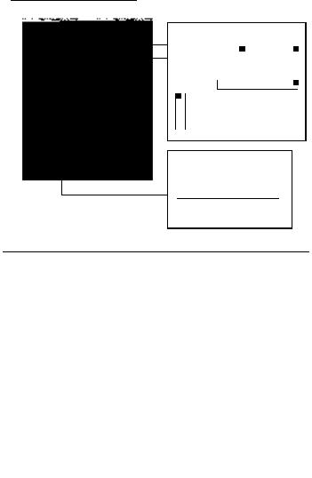
PR5 Mainboard Layout Key
1.ISA Bus Expansion Slots
2.PCI Bus Expansion Slots
3.USB Port Connector
4.Floppy Disk Drive Controller Connector
5.IDE Controller Connectors IDE1 (left) & IDE2 (right)
6.PS/2 Mouse (left) & Keyboard (right) Connectors
7.Power Input Connectors
8.COM1 (left) & COM2 (right) Serial, LPT Parallel Port Connectors
9. SIMM Memory module sockets 1 – 4 (left to right) 10. DIMM Memory module sockets 1 & 2 (left to right) 11. DS DIP switches
12 . CMOS Battery
13. VC DIP switches
14. Flash BIOS Chip
15. COAST PB SRAM cache module socket
16. Heat Sinks
AB –PR5 PCI Mainboard Layout
U l tr a
I O
1 |
2 |
|
|
|
|
|
|
8 2 3 7 1 |
|
|
1 |
|
2 |
|
P I I X 3 |
|
|
|
|
|
|
||
1 |
1 |
3 |
1 |
4 |
1 |
5 |
|
1 |
|
|
|
|
1 6
P e n t i u m C P U
6
7
3 8
4 |
1 |
0 |
5 9
8 2 4 3 7 V X
PB S RA M
4 3 8 V X
PB S RA M |
4 3 8 V X |

System Block Diagram
Section 2
Configuration Quick Reference
PR5 Hardware Configuration:
CPU Configuration
Memory Configuration
L2 Cache Configuration
Onboard Connectors
DIP & Jumper Summary
H a r d w a r e C o n f i g u r a t i o n
This chapter is about how to configure the PR5. The first section is a summary for the experienced user. The second explains the same material in detail. If your PR5 is already installed in a system you can use this section if you need to reconfigure the mainboard.
C o n f i g u r a t i o n Q u i c k R e f e r e n c e
This section provides a summary of the information needed to configure the PR5 mainboard for installation. Please refer to the section PR5 Hardware Configuration for detailed information.
CPU Configuration & Installation
The PR5 has a Socket 7 Zero Insertion Force (ZIF) socket. There are several CPU configuration settings required, including CPU voltage, External Clock Frequency and External Clock Factor. Detailed CPU reference information is in Section 4.
CPU Voltage
The following charts show the CPU voltage DIP switch settings for Intel, AMD and Cyrix CPUs. Reference information on required voltages is in Section 4.
CPU Voltage Settings
You must set the CPU voltage using DIP switch block VC1-8. The switches are labeled on the block. The following charts list the settings.
Default Setting : 3.38V.
See Section 4 for detailed information on determining CPU voltage.
VC DIP Switch Block Location
VC Block
1 |
ON |
2 |
|
3 |
|
4 |
|
5 |
|
6 |
|
7 |
|
8 |
DIP |
|

Intel Pentium CPU Vcore/Vio Settings
Vcore/Vio |
V C 1 |
V C 2 |
V C 3 |
V C 4 |
V C 5 |
V C 6 |
V C 7 |
V C 8 |
|
|
|
|
|
|
|
|
|
2 . 7 V / 3 . 3 V |
O F F |
O F F |
O F F |
O F F |
O N |
O F F |
O F F |
O N |
|
|
|
|
|
|
|
|
|
2 . 8 V / 3 . 3 V |
O F F |
O F F |
O F F |
O N |
O F F |
O F F |
O F F |
O N |
|
|
|
|
|
|
|
|
|
2 . 9 3 V / 3 . 3 V |
O F F |
O F F |
O N |
O F F |
O F F |
O F F |
O F F |
O N |
|
|
|
|
|
|
|
|
|
3 . 3 8 V / 3 . 3 V |
O F F |
O N |
O F F |
O F F |
O F F |
O F F |
O F F |
O N |
|
|
|
|
|
|
|
|
|
3 . 5 2 V / 3 . 3 V |
O N |
O F F |
O F F |
O F F |
O F F |
O F F |
O F F |
O N |
|
|
|
|
|
|
|
|
|
Note: The factory |
default |
setting |
is 3.38V. |
(VRE=3.52V, |
STD/VR=3.38V) |
|
|
|
AMD AMD –K5 CPU Vcore/Vio Settings
Vcore/Vio |
V C 1 |
V C 2 |
V C 3 |
V C 4 |
V C 5 |
V C 6 |
V C 7 |
V C 8 |
|
|
|
|
|
|
|
|
|
2 . 7 V / 3 . 3 8 V |
O F F |
O F F |
O F F |
O F F |
O N |
O F F |
O N |
O F F |
|
|
|
|
|
|
|
|
|
2 . 8 V / 3 . 3 8 V |
O F F |
O F F |
O F F |
O N |
O F F |
O F F |
O N |
O F F |
|
|
|
|
|
|
|
|
|
2 . 9 3 V / 3 . 3 8 V |
O F F |
O F F |
O N |
O F F |
O F F |
O F F |
O N |
O F F |
|
|
|
|
|
|
|
|
|
3 . 3 8 V / 3 . 3 V |
O F F |
O N |
O F F |
O F F |
O F F |
O F F |
O F F |
O N |
|
|
|
|
|
|
|
|
|
3 . 5 2 V / 3 . 3 V |
O N |
O F F |
O F F |
O F F |
O F F |
O F F |
O F F |
O N |
|
|
|
|
|
|
|
|
|
Note: The factory default Vcore setting is 3.38V.
The voltage figures shown are the mid-point of a range, e.g. the range of 3.52V is 3.45V to 3.6V
Cyrix 6x86 CPU Vcore/Vio Settings
Vcore/Vio |
V C 1 |
V C 2 |
V C 3 |
V C 4 |
V C 5 |
V C 6 |
V C 7 |
V C 8 |
|
|
|
|
|
|
|
|
|
2 . 7 V / 3 . 3 V |
O F F |
O F F |
O F F |
O F F |
O N |
O F F |
O F F |
O N |
|
|
|
|
|
|
|
|
|
2 . 8 V / 3 . 3 V |
O F F |
O F F |
O F F |
O N |
O F F |
O F F |
O F F |
O N |
|
|
|
|
|
|
|
|
|
2 . 9 3 V / 3 . 3 V |
O F F |
O F F |
O N |
O F F |
O F F |
O F F |
O F F |
O N |
|
|
|
|
|
|
|
|
|
3 . 3 8 V / 3 . 3 V |
O F F |
O N |
O F F |
O F F |
O F F |
O F F |
O F F |
O N |
|
|
|
|
|
|
|
|
|
3 . 5 2 V / 3 . 3 V |
O N |
O F F |
O F F |
O F F |
O F F |
O F F |
O F F |
O N |
|
|
|
|
|
||||
Note: Recommended setting for 6x86 CPUs is 3.52V/3.3V. |
|
|
|
|
||||
The voltage figures shown are the mid-point of a range, e.g. the range of 3.52V is 3.45V |
to 3.6V |
|||||||
External Clock Frequency & External Clock Factor
The charts in this section show the DIP switch settings for both the CPU external clock frequency and clock factor. Only some of the switches in the DS block apply to these settings.
DS DIP Switch Block Location
External Clock Settings
You must set the correct external clock settings using DIP switch block DS1-8. The switches are labeled on the block. These charts list the settings.
Default Setting : Pentium 133. See Section 4 for detailed CPU information.
DS Block
1 |
ON |
2 |
|
3 |
|
4 |
|
5 |
|
6 |
|
7 |
|
8 |
DIP |
|
Clock Generator Chip
Important Note
The PR5 uses one of several clock generator chips. The DS DIP switch block settings vary depending on which chip is installed. To determine the correct settings you need to know which clock chip is installed. The position of the chip on the mainboard is noted above. The chip part information is printed on the top of the chip. The options are:
ICS :
I C S 9 1 5 9 - 1 4
PhaseLink:
PLL52C59 -14T or PLL52C61-01 or PLL52C61-21
These clock generator chips support a “Normal”and a “Turbo” mode. Normal mode is the CPU manufacturer’s rated clock speed. Turbo mode is an overclock mode that increases the CPU’s clock speed by 2.5% over the Normal rating. For maximum stability and compatibility you should use the Normal mode for the CPU you are installing.

Intel Pentium CPUs
Clock Chip: PLL52C61-01 or PLL52C61-21
|
Ext. Clock Factor |
Ext. Clock Freq.: Normal/Turbo |
ISA |
Spd |
Refresh |
|||
|
|
|
|
|
|
|
|
|
CPU:Ext/Int Clock |
D S 1 |
D S 2 |
D S 3 |
D S 4 |
D S 7 |
D S 5 |
|
D S 6 |
|
|
|
|
|
|
|
||
P 7 5 : 5 0 / 7 5 M H z |
O F F |
O F F |
O N / – O N / – O N / – |
O F F |
|
O F F |
||
|
|
|
|
|
|
|
|
|
P 9 0 : 6 0 / 9 0 M H z |
O F F |
O F F |
O N / O F F |
O N / O F F |
O F F / O N |
O N |
|
O F F |
|
|
|
|
|
|
|
||
P 1 0 0 : 6 6 / 1 0 0 M H z O F F |
O F F |
O F F / O F F O N / O F F |
O N / O F F |
O N |
|
O F F |
||
|
|
|
|
|
|
|
|
|
P 1 2 0 : 6 0 / 1 2 0 M H z O F F |
O N |
O N / O F F |
O N / O F F |
O F F / O N |
O N |
|
O F F |
|
|
|
|
|
|
|
|
||
P 1 3 3 : 6 6 / 1 3 3 M H z O F F |
O N |
O F F / O F F O N / O F F |
O N / O F F |
O N |
|
O F F |
||
|
|
|
|
|
|
|
|
|
P 1 5 0 : 6 0 / 1 5 0 M H z O N |
O N |
O N / O F F |
O N / O F F |
O F F / O N |
O N |
|
O F F |
|
|
|
|
|
|
|
|
||
P 1 6 6 : 6 6 / 1 6 6 M H z O N |
O N |
O F F / O F F O N / O F F |
O N / O F F |
O N |
|
O F F |
||
|
|
|
|
|
|
|
||
P 2 0 0 : 6 6 / 2 0 0 M H z O N |
O F F |
O F F / O F F O N / O F F |
O N / O F F |
O N |
|
O F F |
||
|
|
|
|
|
|
|||
Clock Chip: PLL52C59-14T or ICS9159-14 |
|
|
|
|
|
|||
|
|
|
|
|
|
|||
|
Ext. Clock Factor |
Ext. Clock Freq. — (Norm/Turbo) |
ISA |
Spd |
Refresh |
|||
|
|
|
|
|
|
|
|
|
CPU:Ext/Int Clock |
D S 1 |
D S 2 |
D S 3 |
D S 4 |
D S 7 |
D S 5 |
|
D S 6 |
|
|
|
|
|
|
|
|
|
P 7 5 : 5 0 / 7 5 M H z |
O F F |
O F F |
O N |
O N |
O F F / O N |
O F F |
|
O F F |
|
|
|
|
|
|
|
|
|
P 9 0 : 6 0 / 9 0 M H z |
O F F |
O F F |
O F F |
O N |
O F F / O N |
O N |
|
O F F |
|
|
|
|
|
|
|
|
|
P 1 0 0 : 6 6 / 1 0 0 M H z O F F |
O F F |
O N |
O F F |
O F F / O N |
O N |
|
O F F |
|
|
|
|
|
|
|
|
|
|
P 1 2 0 : 6 0 / 1 2 0 M H z O F F |
O N |
O F F |
O N |
O F F / O N |
O N |
|
O F F |
|
|
|
|
|
|
|
|
|
|
P 1 3 3 : 6 6 / 1 3 3 M H z O F F |
O N |
O N |
O F F |
O F F / O N |
O N |
|
O F F |
|
|
|
|
|
|
|
|
|
|
P 1 5 0 : 6 0 / 1 5 0 M H z O N |
O N |
O F F |
O N |
O F F / O N |
O N |
|
O F F |
|
|
|
|
|
|
|
|
|
|
P 1 6 6 : 6 6 / 1 6 6 M H z O N |
O N |
O N |
O F F |
O F F / O N |
O N |
|
O F F |
|
|
|
|
|
|
|
|
|
|
P 2 0 0 : 6 6 / 2 0 0 M H z O N |
O F F |
O N |
O F F |
O F F / O N |
O N |
|
O F F |
|
|
|
|
|
|
|
|
|
|
N o t e :
ICS9159-14 does not support Turbo mode at 75MHz
ISA Spd. – ISA Bus Clock speed, see page 2-19
Refresh – DRAM refresh [reserved for future use] always OFF
DS8 – reserved for future use, always OFF

A M D –K 5 C P U s (A M D - S S A / 5 & A M D - K 5 )
Clock Chip: PLL52C61-01 or PLL52C61-21
|
Ext. Clock Factor |
Ext. Clock Freq.: Normal/Turbo |
ISA |
Spd |
Refresh |
|||
|
|
|
|
|
|
|
|
|
CPU:Ext/Int Clock |
D S 1 |
D S 2 |
D S 3 |
D S 4 |
D S 7 |
D S 5 |
|
D S 6 |
|
|
|
|
|
|
|
|
|
P R 7 5 : 5 0 / 7 5 M H z |
O F F |
O F F |
O N / — |
O N / — |
O N / — |
O F F |
|
O F F |
|
|
|
|
|
|
|
|
|
P R 9 0 : 6 0 / 9 0 M H z |
O F F |
O F F |
O N / O F F |
O N / O F F |
O F F / O N |
O N |
|
O F F |
|
|
|
|
|
|
|
||
P R 1 0 0 : 6 6 / 1 0 0 M H z O F F |
O F F |
O F F / O F F O N / O F F |
O N / O F F |
O N |
|
O F F |
||
|
|
|
|
|
|
|
|
|
P R 1 2 0 : 6 0 / 9 0 M H z |
O F F |
O F F |
O N / O F F |
O N / O F F |
O F F / O N |
O N |
|
O F F |
|
|
|
|
|
|
|
||
P R 1 3 3 : 6 6 / 1 0 0 M H z O F F |
O F F |
O F F / O F F O N / O F F |
O N / O F F |
O N |
|
O F F |
||
|
|
|
|
|
|
|
|
|
P R 1 5 0 : 6 0 / 1 2 0 M H z O F F |
O N |
O N / O F F |
O N / O F F |
O F F / O N |
O N |
|
O F F |
|
|
|
|
|
|
|
|
||
P R 1 6 6 : 6 6 / 1 3 3 M H z O F F |
O N |
O F F / O F F O N / O F F |
O N / O F F |
O N |
|
O F F |
||
|
|
|
|
|
|
|||
Clock Chip: PLL52C59-14T or ICS9159-14 |
|
|
|
|
|
|||
|
|
|
|
|
|
|||
|
Ext. Clock Factor |
Ext. Clock Freq. — (Norm/Turbo) |
ISA |
Spd |
Refresh |
|||
|
|
|
|
|
|
|
|
|
CPU:Ext/Int Clock |
D S 1 |
D S 2 |
D S 3 |
D S 4 |
D S 7 |
D S 5 |
|
D S 6 |
|
|
|
|
|
|
|
|
|
P R 7 5 : 5 0 / 7 5 M H z |
O F F |
O F F |
O N |
O N |
O F F / O N |
O F F |
|
O F F |
|
|
|
|
|
|
|
|
|
P R 9 0 : 6 0 / 9 0 M H z |
O F F |
O F F |
O F F |
O N |
O F F / O N |
O N |
|
O F F |
|
|
|
|
|
|
|
|
|
P R 1 0 0 : 6 6 / 1 0 0 M H z O F F |
O F F |
O N |
O F F |
O F F / O N |
O N |
|
O F F |
|
|
|
|
|
|
|
|
|
|
P R 1 2 0 : 6 0 / 9 0 M H z |
O F F |
O F F |
O F F |
O N |
O F F / O N |
O N |
|
O F F |
|
|
|
|
|
|
|
|
|
P R 1 3 3 : 6 6 / 1 0 0 M H z O F F |
O F F |
O N |
O F F |
O F F / O N |
O N |
|
O F F |
|
|
|
|
|
|
|
|
|
|
P R 1 5 0 : 6 0 / 1 2 0 M H z O F F |
O N |
O F F |
O N |
O F F / O N |
O N |
|
O F F |
|
|
|
|
|
|
|
|
|
|
P R 1 6 6 : 6 6 / 1 3 3 M H z O F F |
O N |
O N |
O F F |
O F F / O N |
O N |
|
O F F |
|
|
|
|
|
|
|
|
|
|
N o t e :
ICS9159-14 does not support Turbo mode at 75MHz
ISA Spd. – ISA Bus Clock speed, see page 2-19
Refresh – DRAM refresh [reserved for future use] always OFF
DS8 – reserved for future use, always OFF

Cyrix 6x86 CPUs
Clock Chip: PLL52C61-01 or PLL52C61-21
|
Ext. Clock Factor |
Ext. Clock Freq.: Normal/Turbo |
ISA |
Spd |
Refresh |
|||
|
|
|
|
|
|
|
|
|
CPU:Ext/Int Clock |
D S 1 |
D S 2 |
D S 3 |
D S 4 |
D S 7 |
D S 5 |
|
D S 6 |
|
|
|
|
|
|
|
|
|
P 1 2 0 + : 5 0 / 1 0 0 M H z O F F |
O N |
O N / — |
O N / — |
O N / — |
O F F |
|
O F F |
|
|
|
|
|
|
|
|
||
P 1 3 3 + : 5 5 / 1 1 0 M H z O F F |
O N |
O N / — |
O F F / — O N / — |
O N |
|
O F F |
||
|
|
|
|
|
|
|
|
|
P 1 5 0 + : 6 0 / 1 2 0 M H z O F F |
O N |
O N / O F F |
O N / O F F |
O F F / O N |
O N |
|
O F F |
|
|
|
|
|
|
|
|
||
P 1 6 6 + : 6 6 / 1 3 3 M H z O F F |
O N |
O F F / O F F O N / O F F |
O N / O F F |
O N |
|
O F F |
||
|
|
|
|
|
|
|
||
P 2 0 0 + : 7 5 / 1 5 0 M H z O F F |
O N |
O N / — |
O F F / — O F F / — |
O N |
|
O F F |
||
|
|
|
|
|
|
|||
Clock Chip: PLL52C59-14T or ICS9159-14 |
|
|
|
|
|
|||
|
|
|
|
|
|
|||
|
Ext. Clock Factor |
Ext. Clock Freq. — (Norm/Turbo) |
ISA |
Spd |
Refresh |
|||
|
|
|
|
|
|
|
|
|
CPU:Ext/Int Clock |
D S 1 |
D S 2 |
D S 3 |
D S 4 |
D S 7 |
D S 5 |
|
D S 6 |
|
|
|
|
|
|
|
|
|
P 1 2 0 + : 5 0 / 1 0 0 M H z O F F |
O N |
O N |
O N |
O F F / O N |
O F F |
|
O F F |
|
|
|
|
|
|
|
|
|
|
P 1 3 3 + : 5 5 / 1 1 0 M H z O F F |
O N |
O F F |
O F F |
O F F / — |
O N |
|
O F F |
|
|
|
|
|
|
|
|
|
|
P 1 5 0 + : 6 0 / 1 2 0 M H z O F F |
O N |
O F F |
O N |
O F F / O N |
O N |
|
O F F |
|
|
|
|
|
|
|
|
|
|
P 1 6 6 + : 6 6 / 1 3 3 M H z O F F |
O N |
O N |
O F F |
O F F / O N |
O N |
|
O F F |
|
|
|
|
|
|
|
|
|
|
P 2 0 0 + : 7 5 / 1 5 0 M H z O F F |
O N |
O F F |
O F F |
O N / — |
O N |
|
O F F |
|
|
|
|
|
|
|
|
|
|
N o t e :
ICS9159-14 does not support Turbo mode at 75MHz
ISA Spd. – ISA Bus Clock speed, see page 2-19
Refresh – DRAM refresh [reserved for future use] always OFF
DS8 – reserved for future use, always OFF

!
Impo rtant N ote: Double-sided Modules
There is an important limitation in using double-sided SIMM or DIMM modules. Double-sided modules in one bank prevents the use of a corresponding bank of the other type of module. For example:
•If bank SIMM1/2 has 2-sided modules installed, you can not use the DIMM2 socket.
•If bank SIMM3/4 has 2-sided modules installed, you can not use the DIMM1 socket.
•If bank DIMM1 has a 2-sided module installed, you can not use the SIMM3/ 4 sockets.
•If bank DIMM2 has a 2-sided module installed, you can not use the SIMM1/ 2 sockets.
Double-sided modules are modules with memory chips mounted on both sides.
DRAM Installation
The PR5 has numerous possible system memory configurations using the four 72-pin SIMM sockets and the two 168-pin DIMM sockets. The SIMM sockets work in banks of two to provide a 64-bit data path. SIMM1/SIMM2 are one bank, SIMM3/SIMM4 are another. The DIMM sockets are each a bank, for a total of four banks. Please note the following.
•Installed memory is auto-detected by the BIOS
•Minimum installation 2 SIMMs or 1 DIMM module for a 64-bit data path
•Fast Page (FP), EDO and SDRAM are all supported, SDRAM only in DIMM modules
•SIMMs: single or double-sided modules of 4MB and up supported
•DIMMs: single or double-sided modules of 8MB and up supported
•DIMM sockets support both 5-volt (FP or EDO) and 3.3-volt (Unbuffered) DRAM; voltage for both sockets is set by jumper JP11 (see next page)
•Pairs of SIMMs must be the same memory type, size and speed but the type and size of a second pair can be different
•Memory Banks: SIMM1 & SIMM2 SIMM3 & SIMM4 D I M M 1
D I M M 2
•Bank sequence doesn’ t matter, use any combination as long as other requirements are followed
•DRAM speed must be at least 70ns, can be faster
•Parity checking is not supported
•Maximum 128MB supported
There are numerous allowable memory configurations. Since bank sequence is not important, as long as you use SIMMs in pairs you can use any combination of banks.
However, for maximum performance it best to use the same type of DRAM in all banks installed. SDRAM provides higher performance than EDO DRAM and EDO is faster than Fast Page Mode DRAM.
!
DIMM Voltage Settings
Jumper JP11 sets the voltage supplied to the DIMM sockets. FP & EDO modules use the 5-Volt setting.
Default Setting : 3-Volt.
DIMM Voltage Settings
The DIMM sockets support both 5-volt and 3.3-volt unbuffered DRAM. The voltage setting for both DIMM sockets is controlled by jumper JP11. The socket voltage setting must match the voltage of the DRAM on any DIMM modules you install. The jumper settings are shown below.
Jumper JP11 Location
x |
Pi n 1 |
|
|
||
x |
J P 1 1 |
|
x |
||
|
JP 11: DIM M V oltage
|
|
|
Pins 1-2 |
Pins 2-3 |
|
|
|
|
|
|
|
5 |
-Volt |
DIMM |
Short |
N A |
|
|
|
|
|
|
|
3 |
-Volt |
DIMM |
N A |
Short |
[Default] |
|
|
|
|
|
|
N o t e : |
|
|
|
|
|
5 |
-Volt = FP or EDO DRAM |
|
|
|
|
3 |
-Volt |
= 3.3-Volt Unbuffered |
DRAM |
|
|
O n b o a r d C o n n e c t o r s
The PR5 has onboard connector headers for the disk controllers, I/O ports, system enclosure connections and several other features. Pin 1 locations are noted for cable orientation.
Drive Controller & I/O Port Connectors
The PR5 has floppy disk drive, Enhanced IDE controller, serial, parallel and USB port connector headers onboard.
Drive Controller Connectors
The Floppy Disk Drive Controller connector is a 34-pin header. The two Enhanced IDE Controller connectors for Channel 1 and Channel 2 are 40-pin headers. Ribbon cables are supplied for each connector. When installing drives, make sure the colored edge of the drive’ s ribbon cable is at the Pin 1 end of the both the onboard connector and the drive. Their positions and Pin 1 locations are shown below.
F D C
I D E 1 |
I D E 2 |
Controller Connector Locations |
|
|
|
|
|
|
I/O Port Connectors
The PR5 has two serial, one parallel, a connector for an IrDA-compatible Infrared port and a dual-port USB connector onboard. Combination ribbon cable to external port cables are supplied for each connector except the Infrared port. When installing ports, make sure the colored edge of the ribbon cable is at the Pin 1 end of the onboard connector. Their positions and Pin 1 locations are shown below and the pin assignments for the Infrared and USB ports are shown in the table on page 2-11.
I/O Port Connector Locations
I/O Port Connectors
There are five connectors:
JP2: Infrared port (5-pin)
USB: USB ports (16-pin)
COM1: COM1 serial port (10-pin)
COM2: COM2 serial port (10-pin)
LPT: LPT1 printer port (26-pin)
Pin 1: Upper left-hand corner for
USB, upper right-hand corner for
COM & LPT as shown at right.
C O M 1 |
C O M 2 |
LPT
U S B
JP2 IR Connector
x |
x |
x |
x |
x |
|
|
|
|
Pi n 1 |
Connector |
Summary |
|
|
|
|
|
|
N a m e |
# Pins |
Function |
|
|
|
|
|
I D E 1 |
4 0 |
IDE Channel 1 connector |
|
|
|
|
|
I D E 2 |
4 0 |
IDE Channel 2 connector |
|
|
|
|
|
F D C |
3 4 |
Floppy Disk connector |
|
|
|
|
|
LPT |
2 6 |
Parallel Port connector |
|
|
|
|
|
C O M 1 |
1 |
0 |
Serial Port COM1 connector |
|
|
|
|
C O M 2 |
1 |
0 |
Serial Port COM2 connector |
|
|
|
|
U S B |
1 |
6 |
Universal Serial Bus connector |
|
|
|
|
Infrared & USB |
Port |
Connectors |
|
|
|
|
||
|
|
|
|
|
|
|
|
|
|
|
|
|
Pin Function |
|
|||
|
|
|
|
|
|
|
|
|
IR Port |
|
|
|
|
|
|
|
|
|
|
|
|
|
|
|
|
|
Pin |
1 |
|
|
+5-Volts |
DC |
|
||
|
|
|
|
|
|
|
|
|
Pin |
2 |
|
|
Not used |
|
|||
|
|
|
|
|
|
|
|
|
Pin |
3 |
|
|
Receive Data |
|
|||
|
|
|
|
|
|
|
|
|
Pin |
4 |
|
|
Ground |
|
|
|
|
|
|
|
|
|
|
|
|
|
Pin |
5 |
|
|
Transmit Data |
|
|||
|
|
|
|
|
|
|
|
|
USB |
Ports: USB |
1 |
– Pins |
1-8, USB 2 |
– Pins 9-16 |
|
||
|
|
|
|
|
|
|
|
|
Pin |
1 |
|
|
+5-Volts |
|
|||
|
|
|
|
|
|
|
|
|
Pin |
2 |
|
|
Ground |
|
|
|
|
|
|
|
|
|
|
|
|
|
Pin |
3 |
|
|
U S B P 0 |
– |
|
|
|
|
|
|
|
|||||
|
|
|
|
|
|
|
|
|
Pin |
4 |
|
|
Ground |
|
|
U S B |
1 |
|
|
|
|
|
|
|
|
|
Pin |
5 |
|
|
U S B P 0 |
+ |
|
|
|
|
|
|
|
|
||||
|
|
|
|
|
|
|
|
|
Pin |
6 |
|
|
Ground |
|
|
|
|
|
|
|
|
|
|
|
|
|
Pin |
7 |
|
|
Ground |
|
|
|
|
|
|
|
|
|
|
|
|
|
Pin |
8 |
|
|
Ground |
|
|
|
|
|
|
|
|
|
|
|
|
|
Pin |
9 |
|
|
+5-Volts |
|
|||
|
|
|
|
|
|
|
|
|
P in |
10 |
|
|
Ground |
|
|
|
|
|
|
|
|
|
|
|
||
P i n 1 1 |
|
|
U S B P 0 – |
|
|
|
||
|
|
|
|
|||||
|
|
|
|
|
|
|
|
|
P in |
12 |
|
|
Ground |
|
|
U SB |
2 |
|
|
|
|
|
|
|
|
|
P in |
13 |
|
|
U S B P 0 |
+ |
|
|
|
|
|
|
|
|
||||
|
|
|
|
|
|
|
|
|
P in |
14 |
|
|
Ground |
|
|
|
|
|
|
|
|
|
|
|
|
|
P in |
15 |
|
|
Ground |
|
|
|
|
|
|
|
|
|
|
|
|
|
P in |
16 |
|
|
Ground |
|
|
|
|
|
|
|
|
|
|
|
|
|
Note: The USB connector is for two ports. Pins 1 through 8 are for the first port, and pins 9 through 16 are for the second.
System Enclosure Connectors
The system enclosure (case) connections are in a header block which includes the Hardware Reset, Suspend Switch, Turbo LED, Speaker and Keylock connectors. Your system case may or may not have all of these features. The location of the connector block and the pin assignments are shown below.
Enclosure Features Connectors
Enclosure Connectors
There are five connectors in the |
|
|||
block, the other pins are unused: |
3 |
|||
Reset: Pins 1&2 [1] |
|
|
||
Suspend Switch: Pins 6&7 [2] |
2 |
|||
Turbo LED: Pins 8&9 [3] |
|
|||
Speaker: Pins |
11 |
– 14 |
[4 ] |
|
Keylock: Pins |
16 |
– 20 |
[5] |
|
Connectors are labeled at right. |
|
|||
|
|
|
|
1 |
x |
x |
|
|
x |
x |
|
|
x |
x |
5 |
|
x |
x |
|
|
x |
x |
|
|
x |
x |
|
|
x |
x |
|
|
x |
x |
|
|
x |
x |
4 |
|
x |
x |
||
|

Enclosure Features Connectors
Not every pin in the connector block for system case features is used. Which features are used depends on the specific case design. If your case does not have a Keyboard Lock, you can still connect a Power LED lead to Pin 20 and either Pin 16 or 18. Refer to the chart at right for the pin assignments.
Enclosure Features Connector Block
Feature |
|
Pin Function |
|
||
|
|
|
|
|
|
Hardware |
Reset |
Connector |
|
|
|
|
|
|
|
|
|
Pin |
1 |
|
Ground |
|
|
|
|
|
|
|
|
Pin |
2 |
|
Reset signal |
|
|
|
|
|
|
|
|
Suspend |
Switch |
Connector |
|
|
|
|
|
|
|
|
|
Pin |
6 |
|
Ground |
|
|
|
|
|
|
|
|
Pin 7 |
|
Suspend |
|
|
|
|
|
|
|||
Turbo LED Connector |
|
|
|||
|
|
|
|
|
|
Pin |
8 |
|
– Negative |
(anode) |
pin |
|
|
|
|
|
|
Pin |
9 |
|
+ Positive |
(cathode) |
pin |
|
|
|
|
||
Speaker |
Connector |
|
|
||
|
|
|
|
|
|
P i n |
1 1 |
|
+5-Volts DC |
|
|
|
|
|
|
|
|
P in |
12 |
|
Ground |
|
|
|
|
|
|
|
|
P in |
13 |
|
Ground |
|
|
|
|
|
|
|
|
P in |
14 |
|
Sound signal |
|
|
|
|
|
|||
Keylock & Power LED Connector |
|
|
|||
|
|
|
|
|
|
P in |
16 |
|
Ground |
|
|
|
|
|
|
||
P in |
17 |
|
Keyboard inhibit signal |
||
|
|
|
|
|
|
P in |
18 |
|
Ground |
|
|
|
|
|
|
|
|
P in |
19 |
|
Unused |
|
|
|
|
|
|
||
Pin |
20 |
|
+5-Volts DC (for Power LED) |
||
|
|
|
|
|
|
N o t e : |
|
|
|
|
|
Pins |
3,4, |
5, 10, |
15 are unused |
|
|
Other Connectors
There are several other connectors on the PR5, including the power input, keyboard, PS/2 mouse, IDE LED activity light and CPU fan connectors. Their locations and pin assignments are shown below and at right.
Power Input Connector
The system power supply connector is a 12-pin connector, divided into two sections, P8 and P9.
Keyboard & PS/2 Mouse Connectors
The external keyboard connector is a standard “AT” DIN keyboard connector. The PS/2 mouse connector is a 6- pin header block for a PS/2 mouse port.
IDE LED Activity Light Connector
The IDE LED activity light connector is a 4-pin connector header which will accept either a 2-pin or 4-pin IDE LED activity light connector lead.
CPU Fan Power Connector
The CPU fan power connector is a 3-pin connector header which will accept either a 2-pin or 3-pin CPU fan power lead connector.
Connector Locations
|
|
|
|
|
|
|
|
|
J 4 |
J2 |
Keyboard |
||||
|
|
|
|
|
|
|
|
|
P S / 2 |
|
|
|
Po r t |
||
|
|
|
|
|
|
|
|
|
|
|
|||||
|
|
|
|
|
|
|
|
|
Po r t |
|
|
|
|
|
|
|
|
|
|
|
|
|
|
|
|
|
|
|
|
|
|
|
|
|
|
|
|
|
|
|
|
|
|
|
|
|
J 1 |
|
|
|
|
|
|
|
|
|
P 8 |
|
|
|
P 9 |
||
|
|
|
|
|
|
|
|
|
Power |
Connectors |
|||||
J5 IDE LED |
x |
+ |
|
|
|
|
|
JP9 CPU Fan |
Power |
||||||
|
|
|
|
|
|||||||||||
|
|
|
|
|
|
|
|
|
|
|
|
|
|||
|
x |
|
|
|
|
|
|
|
x |
x |
|
|
x |
||
|
x |
|
|
|
|
|
|
|
|
+ |
|
|
1 |
|
|
|
|
|
|
|
|
|
|
|
|
|
|
|
|||
|
|
|
|
|
|
|
|
|
|
|
|
|
|
||
|
x |
+ |
|
|
|
|
|
|
|
|
|
|
|
|
|

Other Onboard Connectors
!
Power Supply Lead Connectors
Some system power supplies have two leads that connect to the J1 power input connector. If this is the case, you must connect the power supply leads so that the black wires are grouped together in the middle.
Power |
Input Connector J1 |
|
|
|
|
|
|
|
|
||
Pin |
1 |
Powergood |
|
||
|
|
|
|
|
|
Pin |
2 |
+5-Volts |
DC |
|
|
|
|
|
|
|
|
Pin |
3 |
+12 -Volts |
|
DC |
|
|
|
|
|
|
|
Pin |
4 |
–12-Volts |
DC |
|
|
|
|
|
|
|
|
Pin |
5 |
Ground |
|
|
|
|
|
|
|
|
|
Pin |
6 |
Ground |
|
|
|
|
|
|
|
|
|
Pin |
7 |
Ground |
|
|
|
|
|
|
|
|
|
Pin |
8 |
Ground |
|
|
|
|
|
|
|
|
|
Pin |
9 |
–5-Volts |
DC |
|
|
|
|
|
|
|
|
P in |
10 |
+5-Volts |
DC |
|
|
|
|
|
|
|
|
P i n |
1 1 |
+5-Volts |
DC |
|
|
|
|
|
|
|
|
P in |
12 |
+5-Volts |
DC |
|
|
|
|
|
|
||
IDE Activity LED Connector J5 |
|
|
|
||
|
|
|
|
|
|
Pin |
1 |
+ Positive |
(cathode) |
pin |
|
|
|
|
|
|
|
Pin |
2 |
– Negative |
(anode) |
pin |
|
|
|
|
|
|
|
Pin |
3 |
– Negative |
(anode) |
pin |
|
|
|
|
|
|
|
Pin |
4 |
+ Positive |
(cathode) |
pin |
|
|
|
|
|
||
CPU Fan Power Connector JP9 |
|
|
|
||
|
|
|
|
|
|
Pin |
1 |
Ground |
|
|
|
|
|
|
|||
Pin |
2 |
+12-Volts DC for fan power |
|||
|
|
|
|
|
|
Pin |
3 |
Ground |
|
|
|
|
|
|
|
|
|
P R 5 H a r d w a r e C o n f i g u r a t i o n
This section describes how to configure the PR5 mainboard hardware in more detail than the Configuration Quick Reference at the beginning of this section. It is intended for users who are less familiar with computer hardware. If your PR5 is already installed in a system you will not need much of this information unless you need to reconfigure your system.
This section covers all the standard features on the board plus the upgrade options. Since you are more likely to need the upgrade options, they come first. The section is organized as follows
•CPU Options & Installation
•System Memory Configuration
•Level 2 Cache Options
•Onboard Connectors
•DIP Switch and Jumper Summary
The information in this section augments the Configuration Quick Reference. So these sections provide additional detail, with some review.
CPU Options & Installation
The PR5 supports a wide assortment of CPU chips from various manufacturers. It is also designed to provide as much upgradability as current information on future CPUs allows. We must note, however, that only the CPUs listed in the manual have been certified to work with the PR5.
Related Terminology
To make it easier to understand the information this section you may want to review the following terms.
Clock
You’ ll see this term used in several ways. Here it doesn’ t refer to keeping time and is not the clock that keeps the date and time setting for the system. The mainboard relies on the system clock to provide digital timing pulses at a constant frequency. The signal the clock generates synchronizes all operations on the board. This “clock frequency” , or the number of signals per second is what we usually think of as the clock “speed” of the system.
In Pentium-based designs there is more than one clock speed. The mainboard components run at one speed and the CPU will run at the same speed in its external activity, but will run at some multiple of that speed internally.
External Clock
The External Clock, also sometimes referred to as the external CPU clock or bus clock, is the CPU’ s input clock. The CPU will interface with other components at this speed and its internal clock speed is a multiple of this external speed. The internal speed is set by the Clock Multiplier Factor. For example, the Intel Pentium P90, P120 and P150 CPUs all have the same external clock, 60MHz, but have different clock factors.
Internal Clock
The Internal Clock is a multiple of the external clock and is the speed used to list the processor’ s operating speed. The internal speed is set by the Clock Multiplier Factor. For example, the Intel Pentium P150 CPU has a 150MHz internal clock speed, a 2.5 multiple of the 60MHz external clock.
Clock Multiplier Factor
The clock multiplier factor is the factor by which the external clock is multiplied to set the CPU’ s internal clock speed. The PR5 has four options: 1.5, 2, 2.5, 3. For example, the Pentium P166 requires a 66MHz external clock and a 2.5 clock multiplier factor to establish its 166MHz internal clock speed. Note: The full clock frequencies are rounded off for convenience when listed, so while 66 x 2.5 = 165, the actual clock speed is 166MHz.
ISA Bus Clock
This is the clock speed of the ISA expansion bus and may also be referred to as the ISA speed, AT Bus Clock or AT clock. The original specification was 8MHz. The slower speed ensures compatibility with all ISA expansion cards. Newer ISA expansion cards may be able to operate at faster speeds, which provide increased performance. The PR5 can be set for slower or faster ISA Bus clock speeds. The slower speed ensures maximum compatibility.

CPU Voltage – Vcore & Vio
The CPU input voltage has two components, Vcore and Vio. Vcore provides the power for internal processing and Vio for the external interface. The two settings are linked, so the VC DIP settings cover both of them.
P–Rating
The “P–Rating” is a categorization used to rate the performance of some Pentium-compatible CPUs. The rating system was created because some CPUs perform at a higher effective speed than their internal clock speed indicates. For example, the Cyrix 6x86 P166+ has a clock speed of 133MHz, but performs at an effective speed equal to or greater than 166MHz. The P–rating indicates the effective, rather than the actual clock speed of the CPU.
CPU Settings
To configure the PR5 for the CPU you will install you have to set the switches on the two CPU configuration DIP switch blocks DS and VC. The procedure is as follows:
|
1. |
Set the Clock Multiplier Factor using switches DS1 |
|
and DS2 on the DS DIP switch block. |
|
|
|
|
|
2. |
Set the External Clock configuration using switches |
|
|
DS3, DS4 and DS7 on the DS DIP switch block. |
|
3. |
Set the ISA Bus Clock configuration using switch |
|
|
DS5 on the DS DIP switch block. |
|
4. |
Make sure DS6 on the DS DIP switch block is OFF. |
|
|
This controls DRAM refresh and is reserved for use |
|
|
with future CPUs. The default setting is OFF. |
|
5. |
Make sure DS8 on the DS DIP switch block is OFF. |
|
|
This is reserved for use with future CPUs. The de- |
|
|
fault setting is OFF. |
|
6. |
Set the Vcore/Vio configuration using the VC DIP |
|
|
switch block. |
|
7. |
Make sure jumper JP10 is set to the default “Open” |
|
|
setting (no jumper cap connecting the two pins). |
In order to give you more CPU configuration options we have included Turbo settings which increase system performance somewhat as well as the standard CPU configurations which maintain maximum stability and compatibility. The Turbo settings are labeled as such and all other settings are standard. The charts on the following pages show the settings for various CPUs.

DS & VC DIP Switch Block Locations
VC Block
1 |
ON |
2 |
|
3 |
|
4 |
|
5 |
|
6 |
|
7 |
|
8 |
DIP |
|
DS Block
1 |
ON |
2 |
|
3 |
|
4 |
|
5 |
|
6 |
|
7 |
|
8 |
DIP |
|
DS5 ISA Bus Clock Settings
External Clock |
D S 5 |
Bus Clock |
|
|
|
5 0 M h z |
O n |
6 . 2 5 M H z |
|
|
|
|
O f f |
8 . 3 3 M H z |
|
|
|
6 0 M H z |
O n |
7 . 5 M H z |
|
|
|
|
O f f |
1 0 M H z |
|
|
|
6 6 M H z |
O n |
8 . 2 5 M H z |
|
|
|
|
O f f |
1 1 M H z |
|
|
|
N o t e :
The suggested setting is highlighted in bold face type in the chart. DS5 ON: ISA Bus Clock = External Clock ÷ 8
DS5 OFF: ISA Bus Clock = External Clock ÷ 6 Factory default setting is ON

Intel Pentium CPU Clock Multiplier Factor
Clock Factor |
D S 1 |
D S 2 |
Clock Factor x External Clock=Internal Clock Speed (in MHz) |
|
|
|
|
1 . 5 |
O F F |
O F F |
1 . 5 x 5 0 = 7 5 ; 1 . 5 x 6 0 = 9 0 ; 1 . 5 x 6 6 = 1 0 0 |
|
|
|
|
2 |
O F F |
O N |
2 x 6 0 = 1 2 0 ; 2 x 6 6 = 1 3 3 |
|
|
|
|
2 . 5 |
O N |
O N |
2 . 5 x 6 0 = 1 5 0 ; 2 . 5 x 6 6 = 1 6 6 |
|
|
|
|
3 |
O N |
O F F |
3 x 6 0 = 1 8 0 ; 3 x 6 6 = 2 0 0 |
|
|
|
|
Note: The factory default setting 2
*The internal clock speed also indicates which Pentium it is for e.g. “75” is for P75, “90” is for P90 etc.
Intel Pentium CPU Vcore/Vio Settings
Vcore/Vio |
V C 1 |
V C 2 |
V C 3 |
V C 4 |
V C 5 |
V C 6 |
V C 7 |
V C 8 |
|
|
|
|
|
|
|
|
|
2 . 7 V / 3 . 3 V |
O F F |
O F F |
O F F |
O F F |
O N |
O F F |
O F F |
O N |
|
|
|
|
|
|
|
|
|
2 . 8 V / 3 . 3 V |
O F F |
O F F |
O F F |
O N |
O F F |
O F F |
O F F |
O N |
|
|
|
|
|
|
|
|
|
2 . 9 3 V / 3 . 3 V |
O F F |
O F F |
O N |
O F F |
O F F |
O F F |
O F F |
O N |
|
|
|
|
|
|
|
|
|
3 . 3 8 V / 3 . 3 V |
O F F |
O N |
O F F |
O F F |
O F F |
O F F |
O F F |
O N |
|
|
|
|
|
|
|
|
|
3 . 5 2 V / 3 . 3 V |
O N |
O F F |
O F F |
O F F |
O F F |
O F F |
O F F |
O N |
|
|
|
|
|
|
|
|
|
Note: The factory |
default |
setting |
is 3.38V. |
(VRE=3.52V, |
STD/VR=3.38V) |
|
|
|
Loading...