

Yaesu VX-5R Service Manual

50/144/430 MHz Triple-Band
Heavy Duty FM Transceiver
VX-5R
Technical Supplement
©2003 VERTEX STANDARD CO., LTD. E126990A
VERTEX STANDARD CO., LTD.
4-8-8 Nakameguro, Meguro-Ku, Tokyo 153-8644, Japan
VERTEX STANDARD
US Headquarters
10900 Walker Street, Cypress, CA 90630, U.S.A.
International Division
8350 N.W. 52nd Terrace, Suite 201, Miami, FL 33166, U.S.A.
YAESU EUROPE B.V.
P.O. Box 75525, 1118 ZN Schiphol, The Netherlands
YAESU UK LTD.
Unit 12, Sun Valley Business Park, Winnall Close
Winchester, Hampshire, SO23 0LB, U.K.
VERTEX STANDARD HK LTD.
Unit 5, 20/F., Seaview Centre, 139-141 Hoi Bun Road,
Kwun Tong, Kowloon, Hong Kong
Introduction
This manual provides the technical information necessary for servicing
the VX-5R Triple-Band Heavy Duty FM Transceiver.
Servicing this equipment requires expertise in handing surface-mount
chip components. Attempts by non-qualified persons to service this
equipment may result in permanent damage not covered by the war-
ranty, and may be illegal in some countries.
Two PCB layout diagrams provided for each double-sided board in
this transceiver. Each side of the board is referred to by the type of the
majority of components installed on that side ("Side A" or "Side B"). In
most cases one side has only chip components, and the other has ei-
ther a mixture of both chip and leaded components (trimmers, coils,
electrolytic capacitors, ICs, etc.), or leaded components only.
While we believe the information in this manual to be correct, VER-
TEX STANDARD assumes no liability for damage that may occur as a
result of typographical or other errors that may be present. Your coop-
eration in pointing out any inconsistencies in the technical informa-
tion would be appreciated.
Contents
Specification.......................................................................................................................................... 2
Exploded View & Miscellaneous Parts ............................................................................................ 3
Block Diagram ...................................................................................................................................... 5
Interconnection Diagram .................................................................................................................... 6
Circuit Description ............................................................................................................................. 7
Alignment ............................................................................................................................................ 11
Board Unit (Schematics, Layouts & Parts)
CNTL Unit ......................................................................................................................................................................17
AF Unit ............................................................................................................................................................................ 35
RF Unit ............................................................................................................................................................................51
VCO Unit ........................................................................................................................................................................ 73

Specifications
General
Frequency Ranges:
Channel Steps:
Frequency Stability:
Repeater Shift (default):
Emission Type:
Antenna Impedance:
Supply Voltage:
Current Consumption:
Operating Temperature:
Case Size:
Weight:
Transmitter
RF Power Output:
Modulation Type:
Maximum Deviation:
Spurious Emission:
Microphone Impedance:
Receiver
Circuit Type:
Intermediate Frequencies:
Sensitivity:
Selectivity:
AF Output:
Rx: 0.5 - 1.8 MHz (BC Band)
1.8 - 16 MHz (SW Band)
48 - 59 MHz (50 MHz HAM)
59 - 108 MHz (FM)
108 - 137 MHz (Air Band)
137 - 174 MHz (144 MHz HAM)
174 - 222 MHz (VHF-TV)
222 - 420 MHz (ACT1: Action Band 1)
420 - 470 MHz (430 MHz HAM)
470 - 729 MHz (UHF-TV)
800 - 999 MHz (ACT2: Action Band 2, Cellular Blocked)
Tx: 50 - 54 MHz
144 - 146 MHz or 144 - 148 MHz
430 - 440 MHz or 430 - 450 MHz
5/9/10/12.5/15/20/25/50/100 kHz
±5 ppm (–10°C to +60°C)
±600 kHz (144 MHz)
±1.6/5.0/7.6 MHz (430 MHz)
F2, F3
50 W
Nominal: 7.2 V DC, Negative Ground
Operating: 10 - 16 V DC, Negative Ground (EXT DC jack)
150 mA (Receive)
55 mA (Standby, Saver Off)
25 mA (Standby, Saver On)
400 µA (Auto Power Off)
1.6 A (5 W Tx, 50 MHz)
1.7 A (5 W Tx, 144 MHz)
1.9 A (4.5 W Tx, 430 MHz)
–20°C to +60°C
58 (W) x 88 (H) x 27 (D) mm (w/o knob & antenna)
255 g
5 W (@ 13.8 V EXT DC IN)
5 W (@ 7.2 V, 50 MHz/144 MHz)
4.5 W (@ 7.2 V, 430 MHz)
Variable Reactance
±5 kHz
At least 60 dB below
2 kW
Double-Conversion Superheterodyne
1st: 47.25 MHz (N-FM)
45.8 MHz (W-FM)
2nd: 450 kHz (N-FM)
10.7 MHz (W-FM)
0.16 µV for 12 dB SINAD (50 - 54 MHz/144-148 MHz, N-FM)
0.9 µV for 12 dB SINAD (76 - 108 MHz/174 - 222 MHz, W-FM)
0.18 µV for 12 dB SINAD (430 - 450 MHz, N-FM)
3 µV for 12 dB SINAD (470 - 729 MHz, except 540-630 MHz, W-FM)
15 kHz/35 kHz (-6 dB/-60 dB: N-FM)
400 mW @ 8 W for 10 % THD (@ 7.2V DC)
Specifications are subject to change without notice, and are guaranteed within amateur bands only.
2
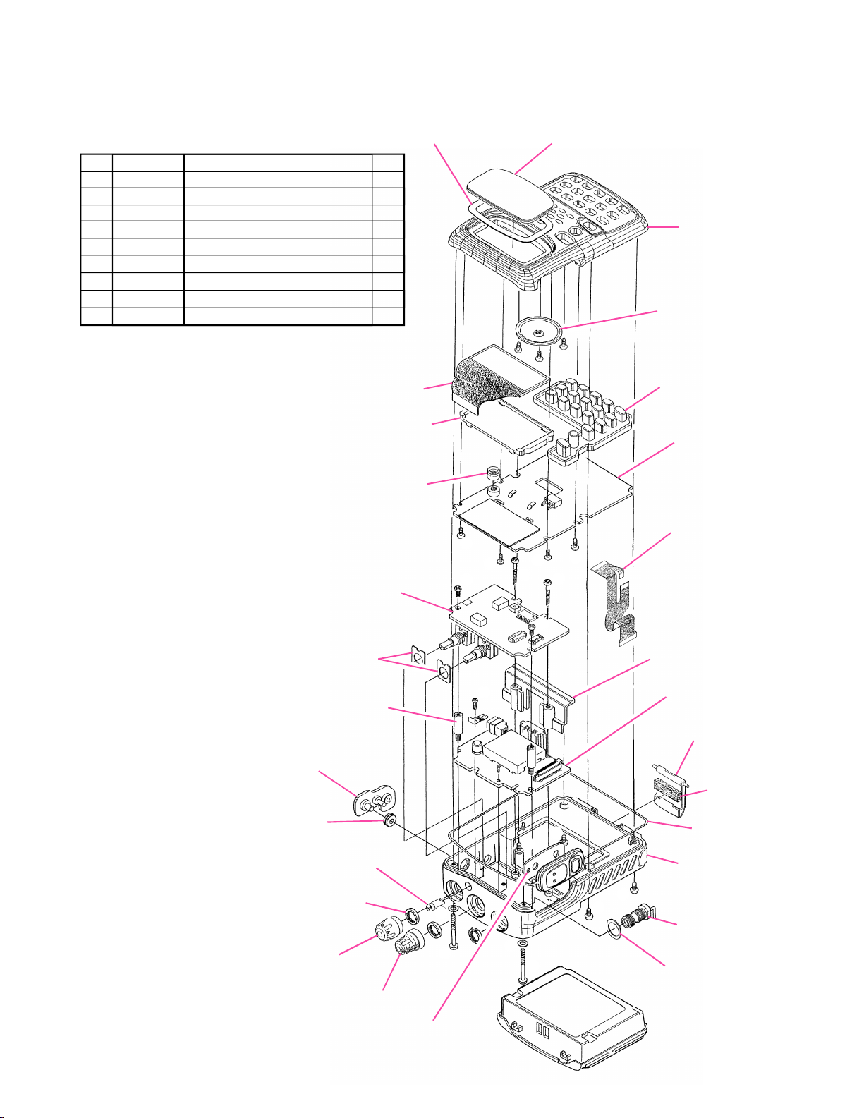
Exploded View & Miscellaneous Parts
No.
À
Á
Â
Ã
Ä
Å
Æ
Ç
È
YAESU P/N
U9900063
U44104002
U44115002
U9900089
U44105007
U20104002
U9900088
U9900090
U9900066
TAPTITE SCREW 2X3.3Ni
TAPTITE SCREW M2X4Ni
TAPTITE SCREW M2X15Ni
TAPTITE SCREW M2X22B
TAPTITE SCREW M2X5B
BINDING HEAD SCREW M2X4Ni
NYLON WASHER WN-1
TAPTITE SCREW M2X3NI (Lot.5-)
TAPTITE SCREW M1.7X3NI#1 (Lot.5-)
Description
Non-designated parts are available only as
part of a designated assembly.
RA0139300
LIGHT GUIDE (LCD)
RA0140200
MIC HOLDER RUBBER
RA0142600
DOUBLE FACE (WINDOW)
Qty.
3
4
2
2
4
2
2
1
1
Q7000291
LCD UNIT
AF UNIT
Á
Å
Á
À
À
Á
Â
RA0139400
WINDOW
À
Á
Â
CP6330003 (USA)
CP6330004 (EXPORT)
CP6330005 (GERMANY)
CP6330006 (KOREA)
CP6330008 (VX 5RS)
PANEL-SUB ASS'Y
M4090130
SPEAKER
RA0138000
RUBBER KNOB (KEY BOARD)
CNTL Unit
FPC CABLE
FR003100B
RA0139800
PACKING PAD(VR/ENC)
RA0139700
STUD (2pcs)
RA0139500
RUBBER CAP
R3152440
PACKING PAD
RA0139600
LIGHT GUIDE
RA0142400
RING NUT (6×0.75) (2pcs)
RA0143600
ENCODER KNOB
RA0143500
VOLUME KNOB
Æ
Ã
RA0140000
TIE PLATE (PTT)
Ç
È
Æ
Ä
Ã
Å
Ä
Ä
RA0139200
HOLDER PLATE
Ä
RF Unit
RA014030A (Lot. 69~)
RA0140300
LATCH NAIL
RA0155600
PACKING SHEET
RA0139100
RUBBER KNOB (PTT)
RA0363100 (VX 5RS)
RA013790A (VX 5R:Lot. 5~)
RA0137900 (VX 5R)
REAR CASE
RA0145000
SMA CONNECTOR ASS'Y
RA0160400 (Lot. 2~)
RA0139900
PACKING PAD (SMA)
3

Note:
4
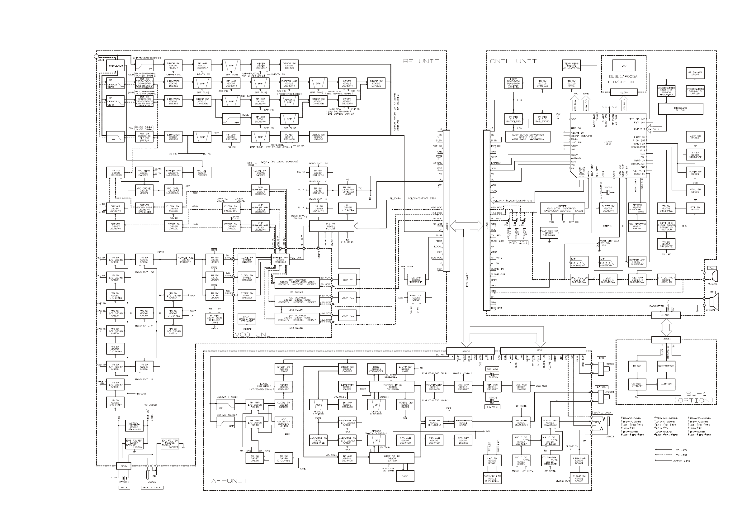
Block Diagram
5

Interconnection Diagram
6

Circuit Description
The VX-5R internal assembly consists of the RF Unit,
Control (CNTL) Unit, and the AF Unit. The RF Unit con-
tains the receiver front end, PLL IC, power and switching
circuits, and the VCO Unit for transmit and receive local
signal oscillation. The CNTL Unit contains the CPU and
audio ICs, as well as the power circuitry for the LCD. The
AF Unit contains the IF, plus audio ICs.
Receiver Signal Flow
The VX-5R includes five receiver front ends, each opti-
mized for a particular frequency range and mode combi-
nation.
(1) Triplexer
Signals between 0.5 and 540 MHz received at the anten-
na terminal pass through an input low-pass filter com-
posed of L3059, L3060, C3176, and C3175.
Received 430 MHz signals then pass through a low-pass
filter, CF3002 (GLP9-450M), to the UHF T/R switch circuit composed of diode switch D3034 (RLS135), D3038
(1SV307), and D3041 (1SV271).
Received 145 MHz signals, after passing through the first
low-pass filter, are passed through low-pass filter CF3003
(GLP8-148M) to the VHF T/R switch circuit, composed of
diode switch D3035 (RLS135), D3039 (1SV307), D3043
(1SV271), and Q3055 (DTC143ZE).
On the 6-meter band, the 50 MHz signals, after passing
through the first low-pass filter, are passed through low-
pass filter L3055, C3164, C3169, and C3163 to the 50 MHz
T/R switch circuit composed of diode switches D3036
(RLS135) and D3040 (1SV307).
(2) 145 MHz Band Reception
Received signals between 140 and 150 MHz pass
through the Triplexer circuit, VHF T/R switch circuit, pro-
tector diode D3003 (1SS362), and 1st VHF band switch
D3010 (DAN235E) before additional filtering by a band-
pass filter consisting of C3023, L3010, and C3032. The sig-
nals are then applied to RF amplifier Q3013 (2SC5374).
The amplified RF signal is band-pass filtered by CF3001
(LFB30N11B0146B010PT) and applied through the 2nd
VHF band switch circuit D3025 (DAN235E) to the first
mixer, Q3020 (2SC5374).
Meanwhile, VHF output from pin 5 of the VCO Unit is
amplified by Q3023 (2SC5374) and applied through diode T/R switch D3030 (DAN222) to mixer Q3020 as the
first local signal.
The 47.25 MHz intermediate frequency product of the
mixer is delivered to the AF Unit.
(3) 435 MHz Band and 222 ~ 540 MHz Reception
Received signals between 430 and 450 MHz pass
through the Triplexer circuit, UHF T/R switch circuit, pro-
tector diode D3002 (1SS362), and a variable band-pass
filter composed of L3006, D3008 (HVC358B), and C3017
before application to RF amplifier Q3007 (2SC5374).
The amplified RF signal is then filtered by a two-stage
variable band-pass filter composed of L3014, D3012
(HVC358B), C3040, C3044, D3015 (HVC358B), C3054, and
L3020, then further amplified by Q3016 (2SC5374). The
output of Q3016 is applied to a variable band pass filter
composed of L3029, D3024 (HVC358B), and C3079 so that
only signals within the desired frequency range are deliv-
ered to the first mixer, Q3019 (2SC5374).
Meanwhile, UHF output from pin 2 of the VCO Unit is
amplified by Q3022 (2SC5374) and applied through diode T/R switch D3032 (HN2D01FU) to mixer Q3019 as the
“430 Local” first local signal. The 47.25 MHz intermedi-
ate frequency product of the mixer is delivered to the AF
Unit.
The “TUNE” voltage from the CPU on the CNTL Unit
is amplified by DC amplifier Q3056 (TC75S51F) and ap-
plied to varactors D3008, D3012, D3015, and D3024 in the
variable frequency band-pass filters. By changing the elec-
trostatic capacitance of the varactors, optimum filter char-
acteristics are provided for each specific operating fre-
quency.
(4) 50 MHz Band and 47 ~ 76 MHz Reception
Received signals between 50 and 54 MHz pass through
the Triplexer circuit, T/R switch circuit, protector diode
D3004 (1SS362), and a variable band-pass filter composed
of L3007, C3015, C3021, L3009, and C3025 before applica-
tion to RF amplifier Q3009 (2SC4400).
The amplified RF signal is then filtered by a two-stage
variable band-pass filter composed of L3017, D3013
(HVC300A), C3047, C3048, D3016 (HVC300A), C3055, and
L3021, then further amplified by Q3009, so that only sig-
nals within the desired frequency range are delivered to
the first mixer, Q3017 (2SC4400).
Meanwhile, 50 MHz output from pin 7 of the VCO Unit
is amplified by Q3024 (2SC5374) and applied through
diode T/R switch D3046 (DAN222) to mixer Q3017 as the
“50 Local” first local signal. The 47.25 MHz intermediate
frequency product of the mixer is delivered to the AF Unit.
The “TUNE” voltage from the CPU on the CNTL Unit
is amplified by DC amplifier Q3056 (TC75S51F) and ap-
plied to varactors D3013 and D3016 in the variable fre-
7

Circuit Description
quency band-pass filters. By changing the electrostatic
capacitance of the varactors, optimum filter characteris-
tics are provided for each specific operating frequency.
(5) 0.5 ~ 16 MHz Reception
Received signals in the MF and HF bands pass through
the Triplexer circuit, T/R switch circuit, and protector di-
ode D3004 (1SS362), then they flow to the AF Unit.
The RF signal is then filtered by a low-pass filter com-
posed of L2014 and C2018 (0.5 ~ 1.8 MHz) or a high-pass
filter composed of C2109 and L2016 (1.8 ~ 16 MHz), then
further amplified by Q2025 (FC119), so that only signals
within the desired frequency range are delivered to the
first mixer, Q2026 (2SC4400).
Meanwhile, 50 MHz output from pin 7 of the VCO Unit
is amplified by Q3024 (2SC5374) and applied through
diode T/R switch D3046 (DAN222) to mixer Q2026 as the
“BC Local” first local signal. The 47.25 MHz intermediate
frequency product of the mixer is delivered to pin 24 of
“Narrow IF” IC Q2005.
(6) 76 ~ 222 MHz Reception
Received signals between 76 and 140 MHz or 150 to 222
MHz pass through the Triplexer circuit, VHF T/R switch
circuit, protector diode D3003 (1SS362), and 1st VHF
band switch D3010 (DAN235E) before additional filter-
ing by a band-pass filter composed of C3024, L3007, and
C3033 prior to application to RF amplifier Q3011
(2SC5374).
The amplified RF signal is then filtered by a variable
band-pass filter composed of D3018, D3019 (HVC362´2),
L3023, D3021 (1T412), C3068, L3026, D3022, and D3023
(HVC362). The output of D3023 is applied to a variable
band pass filter so that only signals within the desired
frequency range are delivered to the first mixer, Q3020
(2SC5374).
Meanwhile, VHF output from pin 5 of the VCO Unit is
amplified by Q3023 (2SC5374) and applied through diode T/R switch D3030 (DAN222) to mixer Q3020 as the
first local signal.
The 45.8 MHz intermediate frequency product of the
mixer is delivered to the AF Unit.
(7) 540 ~ 800 MHz Reception
Received signals between 540 and 800 MHz are high-
pass filtered by C3001, L3003, C3007, L3005, C3014, and
L3008, and then passed through high-band diode switch
D3009 (HSC277) before application to high-band RF amplifier Q3010 (2SC5277). The amplified RF signal is then
8
filtered by a variable band-pass filter composed of D3018,
D3019 (HVC362´2), L3023, D3021 (1T412), C3068, L3026,
D3022, and D3023 (HVC362´2). The output of the filter
is applied to first mixer Q3018 (2SC5277), along with the
800 Local first local signal derived from UHF OUT pin 2
of the VCO Unit, which was amplified by Q3022
(2SC5374) and applied through diode T/R switch D3032.
The 47.25 MHz intermediate frequency product of the
mixer is delivered to the AF Unit.
(8) 47.25 MHz First Intermediate Frequency
The 47.25 MHz first intermediate frequency from the
first mixers is delivered from the RF Unit to the AF Unit
through jacks J3002 and J2002. On the AF Unit, the IF for
AM and FM-narrow signals is passed through NAR/WIDE
switch D2001 (DAP222) and 47.25 MHz monolithic crystal filter XF2001 to Narrow-IF amplifier Q2002 (2SC4400)
for input to pin 24 of Narrow IF IC Q2005 (TK10930V)
after amplitude limiting by D2003 (DA221).
Meanwhile, a portion of the output of reference oscilla-
tor Q2018 (2SC4617) and 11.7 MHz crystal X2001 is multiplied fourfold by Q2013 (2SC4400) to provide the 46.8
MHz second local signal, which is applied to the Narrow-
IF IC. Within the IC, this signal is mixed with the 47.25
MHz first intermediate frequency signal to produce the
450 kHz second intermediate frequency.
This second IF is filtered by ceramic filter CF2001
(CFWM450F) and amplified by the limiting amplifier
within the Narrow IF IC before quadrature detection by
ceramic discriminator CD2001 (CDBM450C7).
Demodulated audio exits from pin 12 of the Narrow IF
IC through Narrow-IF mute analog switch Q2010
(HN1J02FU) and squelch gate Q2020 (2SJ144GR) before
de-emphasis at Q2011 (UMX3N).
The resulting audio is amplified by AF amplifier Q2019
(TDA7233D) and passed through MIC/EAR jack J2003 to
the internal speaker, SP1001, or an external earphone.
(9) Squelch Control
Signal components in the neighborhood of 15 kHz con-
tained in the discriminator output pass through an active
band-pass filter composed of R2019, R2021, R2014, C2025,
and C2029, as well as the operational amplifier between
pins 19 and 20 within Narrow-IF IC Q2005. They are then
rectified by D2002 (DA221) to obtain a DC voltage corre-
sponding to the level of noise. This voltage is applied to
pin 99 of CPU Q1003 (HD6473877UX), which compares
the input voltage with a previously set threshold. When

Circuit Description
the input voltage drops below the threshold, normally due
to the presence of a carrier, squelch gate Q2020
(2SJ144GR) turns on, allowing any demodulated audio
to pass. At the same time, pin 73 of the CPU goes high,
causing the green side of BUSY/TX lamp D2011
(BRPG1211C) to light up.
Transmitter Signal Flow
(1) Modulation
Voice signal input from either built-in microphone
MC1001 (EM-140) on the CNTL Unit or external jack J2003
on the AF Unit is pre-emphasized by C1012 and R1010,
and processed by microphone amplifier Q1014-4
(NJM3403AV) and IDC (instantaneous deviation control)
circuit Q1014-1 to prevent over-modulation, then fed
through an active low-pass filter at Q1014-2.
During CTCSS operation, the voice signal is mixed with
the “TONE ENC” subaudible tone signal from pin 90 of
the CPU and delivered to the RF Unit through jacks J1001
and J3002. During DTMF operation, the DTMF tones from
pin 91 of the CPU are passed to the IDC stage.
(2) 145 MHz Band Transmission
Modulating audio from the CNTL Unit passes through
deviation-setting potentiometer VR1002 to “VHF MOD”
pin 4 of the VCO Unit, which is mounted on the RF Unit.
This signal is applied to varactor D4004 (HVC358B) in the
tank circuit of VHF VCO Q4004 (2SC5374), which oscil-
lates at the desired VHF transmitting frequency. The mod-
ulated VCO signal is buffered by amplifier Q4006
(2SC5374) and Q3023, and delivered through VHF T/R
diode switch D3030 to the RF Unit. The modulated low-
level VHF transmit signal from the VCO is passed through
diode switch D3029 (DAN222) to amplifier Q3027
(2SC5374). The modulated VHF transmit signal from the
VCO is amplified by Q3034 (2SK3074) and RF power amplifier Q3039 (2SK3075) up to 0.1, 0.5, or 5 W (depending
on the power level selected by the operator). The RF out-
put passes through TX diode switch D3035 to low-pass
filter CF3003, to suppress harmonics and spurious prod-
ucts before delivery to the antenna at the antenna termi-
nal.
(3) 145 MHz Band Transmit/Receive Switching
Closing PTT switch S1002 on the CNTL Unit pulls the
base of Q1001 (DTA144EE) low, causing the collector to
go high. This signal is passed to pin 39 (“PTT”) of CPU
Q1003, allowing the CPU to recognize that the PTT switch
has been pushed. When the CPU detects closure of the
PTT switch, pin 13 (“TX”) goes high. This control signal is
delivered to the RF Unit, where it switches Q3054 (UMW1)
and Q3051 (CPH6102) to produce the “TX” control signal
that activates Q3031 (2SA1774). At the same time, PLL
division data is sent to PLL IC Q3021 (FQ7925) from the
CPU, and “RX” pin 4 goes low, to disable the receiver
power saver. Also, Q3041 (UMD6N) is switched so as to
disable the receiver circuits. The red side of the BUSY/TX
lamp D2011 also lights up.
(4) 435 MHz Band Transmission
Modulating audio from the CNTL Unit passes through
deviation-setting potentiometer VR1003 to “VHF MOD”
pin 2 of the VCO Unit, which is mounted on the RF Unit.
This signal is applied to varactor D4001 (HVC355B) in
the tank circuit of UHF VCO Q4002 (2SC5374), which
oscillates at the desired UHF transmitting frequency. The
modulated VCO signal is buffered by amplifier Q4006
(2SC5374) and Q3022, and delivered through UHF T/R
diode switch D3032 to the RF Unit. The modulated low-
level UHF transmit signal from the VCO is passed through
diode switch D3029 (DAN222) to amplifier Q3027
(2SC5374), then amplified by driver Q3034 (2SK3074)
and RF power amplifier Q3039 (2SK3075) up to 0.1, 0.5
or 4.5 W (depending on the power level selected by the
operator). The RF output passes through TX diode switch
D3034 and low-pass filtered at CF3002 to suppress har-
monics and spurious products before delivery to the an-
tenna at the antenna terminal.
(5) 435 MHz Band Transmit/Receive Switching
Closing “PTT” switch S1002 on the CNTL Unit pulls
the base of Q1001 (DTA144EE) low, causing the collector
to go high. This signal is passed to pin 39 (“PTT”) of CPU
Q1003, allowing the CPU to recognize that the PTT switch
has been pushed. When the CPU detects closure of the
PTT switch, pin 13 (“TX”) goes high. This control signal is
delivered to the RF Unit, where it switches Q3054 (UMW1)
and Q3051 (CPH6102) to produce the “TX” control signal
that activates Q3032 (2SA1774). At the same time, PLL
division data is sent to PLL IC Q3021 (FQ7925) from the
CPU, and “RX” pin 4 goes low, to (A) disable the receiver
power saver and (B) switch Q3041 (UMD6N) to disable
the receiver circuits. The red side of BUSY/TX lamp D2011
lights up under this condition.
9

Circuit Description
(6) 50 MHz Band Transmission
Modulating audio from the CNTL Unit passes through
deviation-setting potentiometer VR1001 to “50 MHz
MOD” pin 6 of the VCO Unit, which is mounted on the
RF Unit. This signal is applied to varactors D4007 and
D4008 (HVC300A´2) in the tank circuit of VHF VCO
Q4005 (2SC5374), which oscillates at the desired 50 MHz
transmitting frequency. The modulated VCO signal is buff-
ered by amplifier Q4006 (2SC5374) and Q3024, and delivered through 50 MHz T/R diode switch D3033 (1SS355)
to the RF Unit. The modulated low-level 50 MHz trans-
mit signal from the VCO is passed through diode switch
D3033 to amplifier Q3029 (2SC5374), then amplified by
RF power amplifier Q3039 (2SK3075) up to 0.1, 0.5 or 5
W (depending on the power level selected by the opera-
tor). The RF output passes through TX diode switch D3036
and low-pass filtered by L3055, C3164, C3169, and C3163
to suppress harmonics and spurious products before de-
livery to the antenna at the antenna terminal.
(7) 50 MHz Band Transmit/Receive Switching
Closing “PTT” switch S1002 on the CNTL Unit pulls
the base of Q1001 (DTA144EE) low, causing the collector
to go high. This signal is passed to pin 39 (“PTT”) of CPU
Q1003, allowing the CPU to recognize that the PTT switch
has been pushed. When the CPU detects closure of the
PTT switch, pin 13 (“TX”) goes high. This control signal is
delivered to the RF Unit, where it switches Q3054 (UMW1)
and Q3051 (CPH6102) to produce the TX control signal
that activates Q3030 (2SA1774). At the same time, PLL
division data is sent to PLL IC Q3021 (FQ7925) from the
CPU, and “RX” pin 4 goes low, to (A) disable the receiver
power saver and (B) switch Q3041 (UMD6N) to disable
the receiver circuits. The red side of BUSY/TX lamp D2011
lights up under this condition.
PLL Frequency Synthesizer
PLL IC Q3021 on the RF Unit consists of a data shift
register, reference frequency divider, phase comparator,
charge pump, intermittent operation control circuit, and
band selector switch. Serial PLL data from the CPU is con-
verted into parallel data by the shift register in the PLL IC
and is latched into the comparative frequency divider and
reference frequency divider to set a frequency dividing
ratio for each. An 11.7 MHz reference signal produced by
X2001 and Q2018 (2SC4617) on the AF Unit is sent to
“REF” pin 12 of the PLL IC. The internal reference fre-
quency divider divides the 11.7 MHz reference by 2,050
(or 1,640) to obtain a reference frequency of 5 kHz (or 6.25
kHz), which is applied to the phase comparator. Mean-
while, a sample of the output of VHF VCO Q4004
(2SC5374), UHF VCO Q4002 (2SC5374), or 50 MHz VCO
Q4005 (2SC5374) is buffered by Q4006 (2SC5374), then
passed to pin 8 of the PLL IC, where it is frequency-divid-
ed by the internal comparative frequency divider to pro-
duce a comparative frequency which is applied to the
phase comparator. The phase comparator compares the
phase between the reference frequency and comparative
frequency, producing an output pulse corresponding to
the phase difference between them. This pulse is sent to
the charge pump, and the output from the charge pump
passes through a loop filter composed of L3034, R3079,
C3097, and either R3084, C3104, R3088, and C3109 for
VHF, or R3083, C3103, R3087 and C3108 for UHF, or
C3099, R3085, C3105, R3089 and C3110 for 50 MHz, which
convert the pulse into a corresponding smoothed varac-
tor control voltage (VCV). The VCV is applied to varactor
D4004 in the VHF VCO tank circuit, or to varactor D4001
in the UHF VCO tank circuit, or to varactors D4007 and
D4008 in the 50 MHz VCO, to eliminate phase difference
between the reference frequency and comparative frequen-
cy, thereby locking the VCO oscillation frequency to the
reference crystal. The VCO frequency is determined by
the frequency dividing ratio sent from the CPU to the PLL
IC. During receiver power save operation, the PLL circuit
operates intermittently to reduce current consumption,
and the “intermittent operation control” circuit reduces
the lock-up time in this mode of operation.
10
Alignment
Introduction
The VX-5R is carefully aligned at the factory for the spec-
ified performance across the amateur band. Realignment
should therefore not be necessary except in the event of a
component failure. If a sudden problem occurs during
normal operation, it is likely due to component failure;
realignment should not be done until after the faulty com-
ponent has been replaced.
The following procedures cover the adjustments that are
not normally required once the transceiver has left the
factory. However, if damage occurs and some parts sub-
sequently are replaced, realignment may be required.
We recommend that servicing be performed only by au-
thorized VERTEX STANDARD service technicians who
are experienced with the circuitry and fully equipped for
repair and alignment. If a fault is suspected, contact the
dealer from whom the transceiver was purchased for in-
structions regarding repair. Authorized VERTEX STAN-
DARD service technicians realign all circuits and make
complete performance checks to ensure compliance with
factory specifications after replacing any faulty compo-
nents. Those who do undertake any of the following align-
ments are cautioned to proceed at their own risk. Prob-
lems caused by unauthorized attempts at realignment are
not covered by the warranty policy. Also, Yaesu reserves
the right to change circuits and alignment procedures in
the interest of improved performance, without notifying
owners.
Under no circumstances should any alignment be at-
tempted unless the normal function and operation of the
transceiver are clearly understood, the cause of the mal-
function has been clearly pinpointed and any faulty com-
ponents replaced, and realignment determined to be ab-
solutely necessary.
The following test equipment (and familiarity with its
use) is necessary for complete realignment. Correction of
problems caused by misalignment resulting from use of
improper test equipment is not covered under the war-
ranty policy. While most steps do not require all of the
equipment listed, the interactions of some adjustments
may require that more complex adjustments be performed
afterwards.
Do not attempt to perform only a single step unless it is
clearly isolated electrically from all other steps. Have all
test equipment ready before beginning and, follow all of
the steps in a section in the order presented.
Required Test Equipment
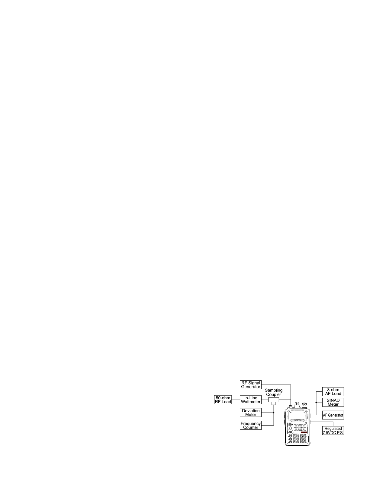
m RF Signal Generator with calibrated output level at 500 MHz
m Deviation Meter (linear detector)
m In-line Wattmeter with 5% accuracy at 500 MHz
m 50-ohm, 10-W RF Dummy Load
m 8-ohm AF Dummy Load
m Regulated DC Power Supply adjustable from 3 to 15 V DC, 2A
m Frequency Counter: 0.2-ppm accuracy at 500 MHz
m AF Signal Generator
m AC Voltmeter
m DC Voltmeter: high impedance
m UHF Sampling Coupler
m SINAD Meter
Alignment Preparation & Precautions
A 10-ohm RF load and in-line wattmeter must be con-
nected to the main antenna jack in all procedures that call
for transmission, as accurate alignment is not possible with
an antenna. After completing one step, read the next step
to see if the same test equipment is required. If not, re-
move the test equipment (except dummy load and watt-
meter, if connected) before proceeding.
Correct alignment requires that the ambient tempera-
ture be the same as that of the transceiver and test equip-
ment, and that this temperature be held constant between
20~30°C (68~86°F). When the transceiver is brought into
the shop from hot or cold air, it should be allowed some
time to come to room temperature before alignment.
Whenever possible, alignments should be made with os-
cillator shields and circuit boards firmly affixed in place.
Also, the test equipment must be thoroughly warmed up
before beginning.
Note: Signal levels in dB referred to in the alignment procedure
are based on 0 dBµ=0.5 µV (closed circuit).
Test Setup
Set up the test equipment as shown below for transceiver
alignment, and apply 7.5 V DC power to the transceiver.
Refer to the drawings for Alignment Points.
Alignment Setup
11
Alignment
PLL Reference Frequency
With the wattmeter, dummy load, and frequency counter
connected to the antenna jack, set the transceiver frequen-
cy to 435.000 MHz. Transmit, and adjust TC1001 on the
AF Unit, if necessary, so the counter frequency is within
100 Hz of the displayed frequency on the VX-5R.
50 MHz band Tx Deviation Adjustment
m With the wattmeter, dummy load and deviation meter
connected to the antenna jack, set the transceiver to
52.000 MHz. Inject a 1 kHz audio tone at a level of 80
mV (rms) to the MIC jack.
m Transmit, and adjust VR1001 to obtain ±4.2-4.5 kHz de-
viation, as indicated on the deviation meter (±3.7-4.0 kHz
for A1, A2A, A2B, and A3 versions).
144 MHz band Tx Deviation Adjustment
m With the wattmeter, dummy load and deviation meter
connected to the antenna jack, set the transceiver to the
center of the 144 MHz band (145 MHz or 146 MHz).
Inject a 1 kHz audio tone at a level of 80 mV (rms) to the
MIC jack.
m Transmit, and adjust VR1002 to obtain ±4.2-4.5 kHz de-
viation, as indicated on the deviation meter (±3.7-4.0 kHz
for A1, A2A, A2B and A3 versions).
430 MHz band Tx Deviation Adjustment
m With the wattmeter, dummy load and deviation meter
connected to the antenna jack, set the transceiver to the
center of the 430 MHz band (435 MHz or 440 MHz).
Inject a 1 kHz audio tone at a level of 80 mV (rms) to the
MIC jack.
m Transmit, and adjust VR1003 to obtain ±4.2-4.5 kHz de-
viation, as indicated on the deviation meter (±3.7-4.0 kHz
for A1, A2A, A2B and A3 versions).
CTCSS Tx Deviation Adjustment
m With the wattmeter, dummy load and deviation meter
connected to the antenna jack, set the transceiver to the
center of 144 MHz band, and enable the CTCSS encod-
er at a frequency of 88.5 Hz.
m Transmit, and adjust VR1004 to obtain ±0.6-0.8 kHz as
indicated on the deviation meter.
FM Wide Alignment
m With the transceiver and RF signal generator both tuned
to 78.1 MHz, modulate the RF signal generator with a 1
kHz tone at a deviation of ±20 kHz, at a level of +40 dBµ
at the antenna jack.
m Adjust T2001 for optimum quieting as indicated on the
SINAD meter.
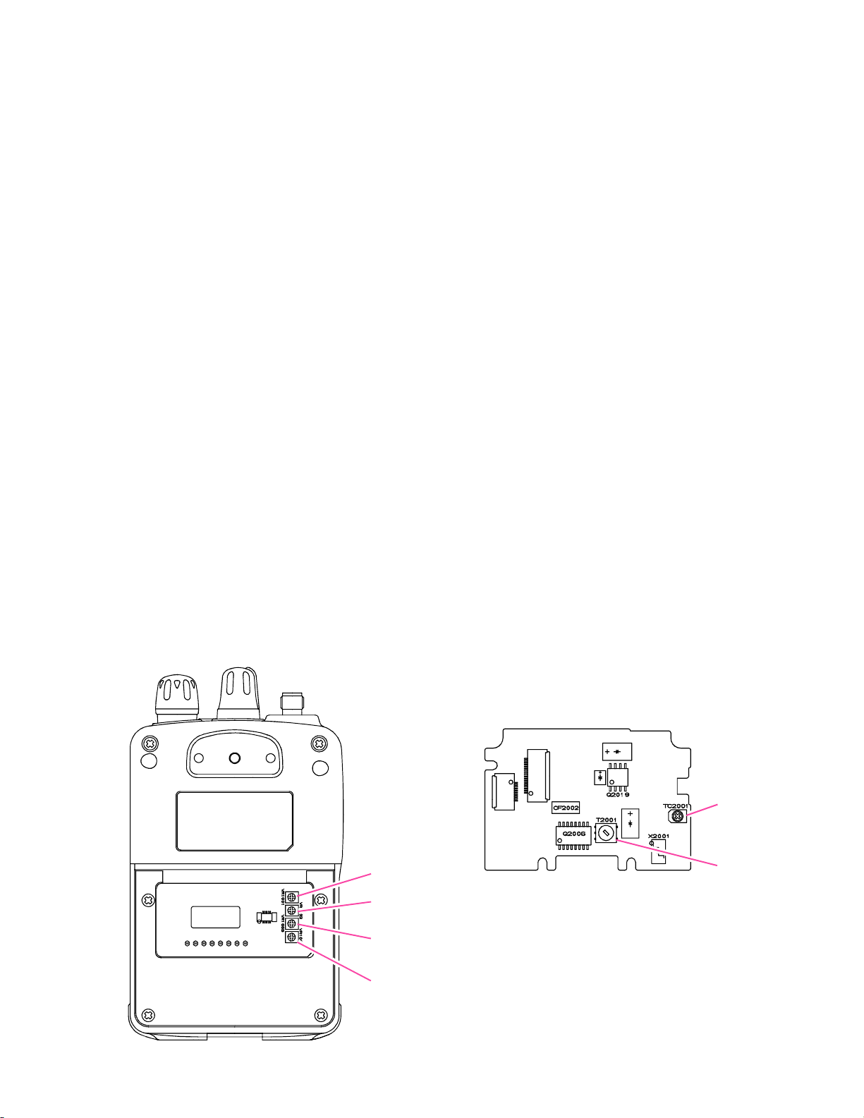
Back of the Transceiver Body
VR1001
VR1002
VR1003
VR1004
TC2001
T2001
12
Alignment Points

Internal System Alignment Routine
This uses a programmed routine in the transceiver which
simplifies many previously complex discrete component
settings and adjustments with digitally-controlled settings
via front panel buttons and LCD indications. Transceiver
adjustments include:
m Squelch Hysteresis
m Squelch Threshold & Tight Adjustment
m S-Meter Full Scale & S-1 Adjustment
m Wide-FM S-Meter Full Scale & S-1 Adjustment
m Power Output Adjustment (Hi/L3/L2/L1)
Alignment
DIAL to select the next setting.
Squelch Preset Tight (TIGH SQL) [54]
m Adjust the generator level to –4.0 dBµ, then presses the
MR button twice. Rotate the DIAL to select the next set-
ting.
S-Meter S-1 Adjustment (S1 LEVEL) [12]
m Adjust the generator level to –7.0 dBµ (1 kHz tone @
±3.5 kHz deviation), then presses the MR button twice.
Rotate the DIAL to select the next setting.
To begin, set the transceiver to the center of the 50 MHz,
144 MHz, and 430 MHz bands. Next, select the 50 MHz
band, then turn the transceiver off.
Now, press and hold the BAND, TXPO and 0 button
together while powering the radio on again. The display
will show the first setting.
Note that the first few settings are not adjustable and
are left as set from the factory.
In the alignment process, each adjustment is selected by
rotating the DIAL. Alignment is performed by:
m Pressing the MR button;
m Injecting a signal of the required frequency and level;
then
m Pressing the MR button after a level setting or adjust-
ment is made. This second pressing of the MR button
stores the entry.
To exit the alignment routine, press the HOME button.
After performing the system alignment in its entirety, in-
dividual settings can be returned to and adjusted should
the need arise.
In the section to follow, typical default values (as set at
the factory) are shown in brackets (e.g. [119]), to serve as a
general guideline. As each transceiver is individually op-
timized at the factory, the precise settings for the trans-
ceiver on your bench may be slightly different.
S-Meter Full-Scale Adjustment (S9 LEVEL) [106]
m Adjust the generator level to +20 dBµ (1 kHz tone @
±3.5 kHz deviation), then presses the MR button twice.
Rotate the DIAL to select the next setting.
Wide-FM S-Meter S-1 Adjustment (S1 LEVEL) [13]
m Adjust the generator level to –0 dBµ (1 kHz tone @ ±20
kHz deviation), then presses the MR button twice. Rotate the DIAL to select the next setting.
Wide-FM S-Meter Full-Scale Adjustment (S9 LEVEL) [131]
m Adjust the generator level to +20 dBµ (1 kHz tone @ ±20
kHz deviation), then presses the MR button twice. Rotate the DIAL to select the next setting.
High TX Power Adjustment (HI POWER) [112]
m Transmit, and adjust the output power level for 5.1-5.5
W by rotating the DIAL, then presses the MR button
twice. Rotate the DIAL to select the next setting.
L3 Tx Power Adjustment (L3 POWER) [74]
m Transmit, and adjust the output power level for 2.3-2.7
W by rotating the DIAL, then presses the MR button
twice. Rotate the DIAL to select the next setting.
L2 Tx Power Adjustment (L2 POWER) [42]
m Transmit and adjust the output power level for 0.8-1.2
W by rotating the DIAL, then presses the MR button
twice. Rotate the DIAL to select the next setting.
50 MHz Band Alignment
Squelch Hysteresis Adjustment (HIS SQL) [0]
m Press the MR button, then rotate the DIAL for minimum
squelch hysteresis. Press the MR button, then rotate the
DIAL to select the next setting.
Squelch Preset Threshold (THLD SQL) [88]
m Inject a –15.0 dBµ RF signal (1 kHz tone @ ±3.5 kHz
deviation), then presses the MR button twice. Rotate the
L1 Tx Power Adjustment (L1 POWER) [21]
m Transmit, and adjust the output power level for 0.2-0.4
W by rotating the DIAL, then presses the MR button twice.
This completes the 50 MHz band internal alignment rou-
tine; press the BAND button to activate the 144 MHz band
internal alignment routine.
13

Alignment
144 MHz Band Alignment
Squelch Hysteresis Adjustment (HIS SQL) [0]
m Press the MR button, then
squelch hysteresis. Press the MR button, then rotate the
to select the next setting.
Squelch Preset Threshold (THLD SQL) [92]
m Inject a –15.0 dBµ RF signal (1 kHz tone @ ±3.5 kHz
deviation), then presses the MR button twice. Rotate the
DIAL to select the next setting.
Squelch Preset Tight (TIGH SQL) [44]
m Adjust the generator level to –4.0 dBµ, then presses the
MR button twice. Rotate the DIAL to select the next set-
ting.
S-Meter S-1 Adjustment (S1 LEVEL) [24]
m Adjust the generator level to –7.0 dBµ (1 kHz tone @
±3.5 kHz deviation), then presses the MR button twice.
Rotate the DIAL to select the next setting.
S-Meter Full-Scale Adjustment (S9 LEVEL) [120]
m Adjust the generator level to +20 dBµ (1 kHz tone @
±3.5 kHz deviation), then presses the MR button twice.
Rotate the DIAL to select the next setting.
Wide-FM S-Meter S-1 Adjustment (S1 LEVEL) [51]
m Adjust the generator level to –0 dBµ (1 kHz tone @ ±20
kHz deviation), then presses the MR button twice. Rotate the DIAL to select the next setting.
Wide-FM S-Meter Full-Scale Adjustment (S9 LEVEL) [170]
m Adjust the generator level to +20 dBµ (1 kHz tone @ ±20
kHz deviation), then presses the MR button twice. Rotate the DIAL to select the next setting.
High TX Power Adjustment (HI POWER) [118]
m Transmit, and adjust the output power level for 5.1-5.5
W by rotating the DIAL, then presses the MR button
twice. Rotate the DIAL to select the next setting.
L3 Tx Power Adjustment (L3 POWER) [76]
m Transmit, and adjust the output power level for 2.3-2.7
W by rotating the DIAL, then presses the MR button
twice. Rotate the DIAL to select the next setting.
L2 Tx Power Adjustment (L2 POWER) [44]
m Transmit, and adjust the output power level for 0.8-1.2
W by rotating the DIAL, then presses the MR button
twice. Rotate the DIAL to select the next setting.
rotate the
DIAL
for minimum
DIAL
L1 Tx Power Adjustment (L1 POWER) [21]
m Transmit, and adjust the output power level for 0.2-0.4
W by rotating the DIAL, then presses the MR button twice.
This completes the 144 MHz band internal alignment
routine; press the BAND button to activate the 430 MHz
band internal alignment routine.
UHF band Alignment
Squelch Hysteresis Adjustment (HIS SQL) [0]
m Press the MR button, then rotate the DIAL for minimum
squelch hysteresis. Press the MR button, then rotate the
DIAL to select the next setting.
Squelch Preset Threshold (THLD SQL) [86]
m Inject a –15.0 dBµ RF signal (1 kHz tone @ ±3.5 kHz
deviation), then presses the MR button twice. Rotate the
DIAL to select the next setting.
Squelch Preset Tight (TIGH SQL) [55]
m Adjust the generator level to –4.0 dBµ, then presses the
MR button twice. Rotate the DIAL to select the next set-
ting.
S-Meter S-1 Adjustment (S1 LEVEL) [7]
m Adjust the generator level to –7.0 dBµ (1 kHz tone @
±3.5 kHz deviation), then presses the MR button twice.
Rotate the DIAL to select the next setting.
S-Meter Full-Scale Adjustment (S9 LEVEL) [96]
m Adjust the generator level to +20 dBµ (1 kHz tone @
±3.5 kHz deviation), then presses the MR button twice.
Rotate the DIAL to select the next setting.
Wide-FM S-Meter S-1 Adjustment (S1 LEVEL) [13]
m Adjust the generator level to 0 dBµ (1 kHz tone @ ±20
kHz deviation), then presses the MR button twice. Rotate the DIAL to select the next setting.
Wide-FM S-Meter Full-Scale Adjustment (S9 LEVEL) [134]
m Adjust the generator level to +20 dBµ (1 kHz tone @ ±20
kHz deviation), then presses the MR button twice. Rotate the DIAL to select the next setting.
High TX Power Adjustment (HI POWER) [172]
m Transmit, and adjust the output power level for 4.6-5.0
W by rotating the DIAL, then presses the MR button
twice. Rotate the DIAL to select the next setting.
14

Alignment
L3 Tx Power Adjustment (L3 POWER) [119]
m Transmit, and adjust the output power level for 2.3-2.7
W by rotating the DIAL, then presses the MR button
twice. Rotate the DIAL to select the next setting.
L2 Tx Power Adjustment (L2 POWER) [69]
m Transmit, and adjust the output power level for 0.8-1.2
W by rotating the DIAL, then presses the MR button
twice. Rotate the DIAL to select the next setting.
L1 Tx Power Adjustment (L1 POWER) [35]
m Transmit, and adjust the output power level for 0.2-0.4
W by rotating the DIAL, then presses the MR button twice.
This completes the internal alignment routine for all bands.
To save all settings and exit, press the HOME button.
15

Alignment
Note:
16
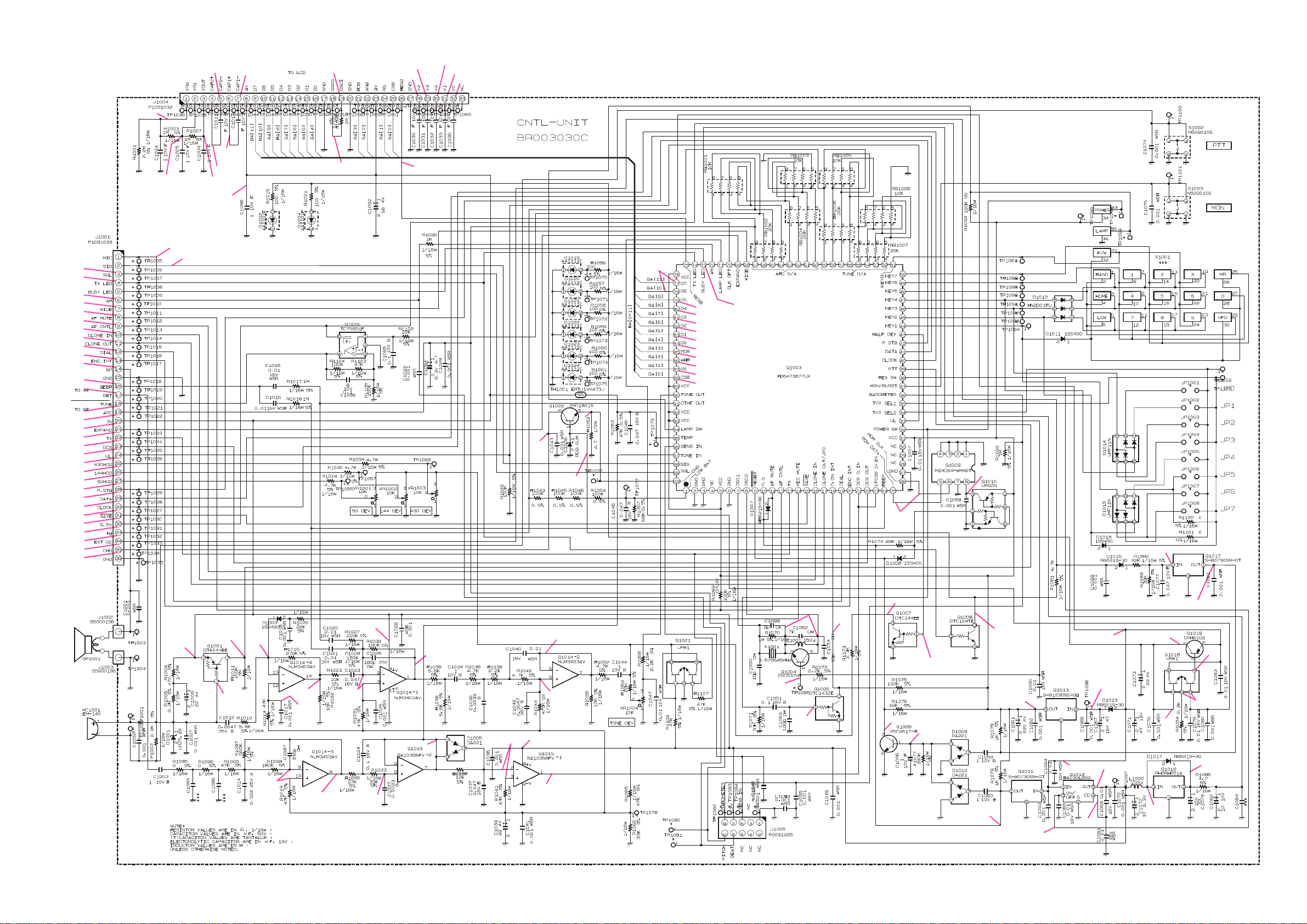
Circuit Diagram
1.0V(0V)
0V(3.0V)
0V(0V)[2.6V]
0V(0V){2.6V}
3.0V(3.0V)
2.9V(2.9V)
3.0V(3.0V)
3.0V(3.0V)
3.0V(3.0V)
3.0V(3.0V)
0V(0V)
0V(0V)
3.0V(3.0V)
4.3V(4.3V)
6.4V(6.4V)
3.0V(1.2V)
3.0V(3.0V)
9.0V(9.0V)
3.0V(3.0V)
0.2V(0V)
1.6V(1.6V)
4.6V
(4.6V)
6.0V(6.0V)
1.5V(1.5V)
1.7V(1.7V)
2.0V(2.0V)
1.0V(1.0V)
4.0V(4.0V)
3.0V(3.0V)
5.1V(5.1V)
6.1V(6.1V)
0V(0V)
0V(0V)
0V(0V)
0V(0V)
0V(0V)
3.0V(3.0V)
0V(0V)
0V(0V)
3.0V(3.0V)
0V(0V)
3.0V(3.0V)
BUSY LED ON: 3.0V
0V(0V)
CNTL Unit
1.7V(0V)
0V(1.8V)
3.0V(3.0V)
0.1V(0.1V)
0V(3.0V)
1.5V(2.2V)
0V(0V)
0V(0V)
0V(0V)
0V(0V)
3.0V(0V)
0V(0V)
0V(0V)
3.0V(3.0V)
6.5V(6.5)
7.3V(6.7V)
7.5V(7.1V)
0V(0V)
3.0V
(3.0V)
0V(3.0V)
2.4V
(1.2V)
2.5V
(0V)
0V(0V)
1.2V
(0V)
1.2V
(0V)
3.0V(0V)
1.2V(1.2V)
1.2V(0V)
1.2V(1.2V)
0V
(0V)
1.3V(0V)
0.5V(0V)
3.0V(3.0V)
0.7V(0V)
0V
(0V)
2.4V
(2.4V)
1.8V(1.8V)
0.3V
(0V)
3.0V
(0V)
3.0V(0V)
0V(0V)
3.0V(0V)
3.0V(0V)
0V(0V)
3.0V(0V)
0.7V(0V)
3.0V(0V)
7.3V(0V)
7.1V(0V)
2.4V(0V)
0.5V(0V)
0.5V
(0V)
0.3V(0V)
6.8V(0V)
0V(0V)
1.2V
(1.2V)
1.2V(1.2V)
1.2V(1.2V)
×× : RX
(××) : TX
[××] : AM RX
{××} : FM-W RX
2.0V(2.0V)
7.3V(0V)
3.0V(0V)
7.3V(0V)
1.3V(0V)
3.0V(0V)
3.0V
(0V)
6.5V(0V)
17

CNTL Unit
Note:
18
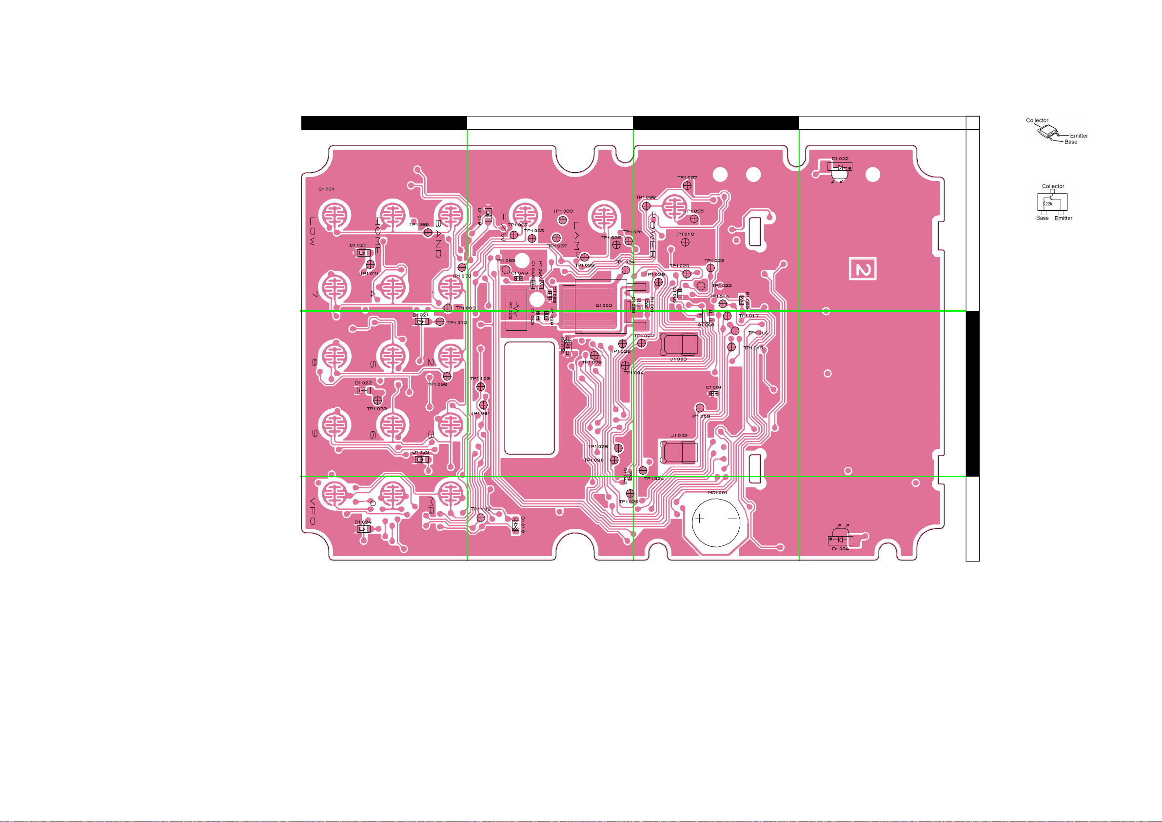
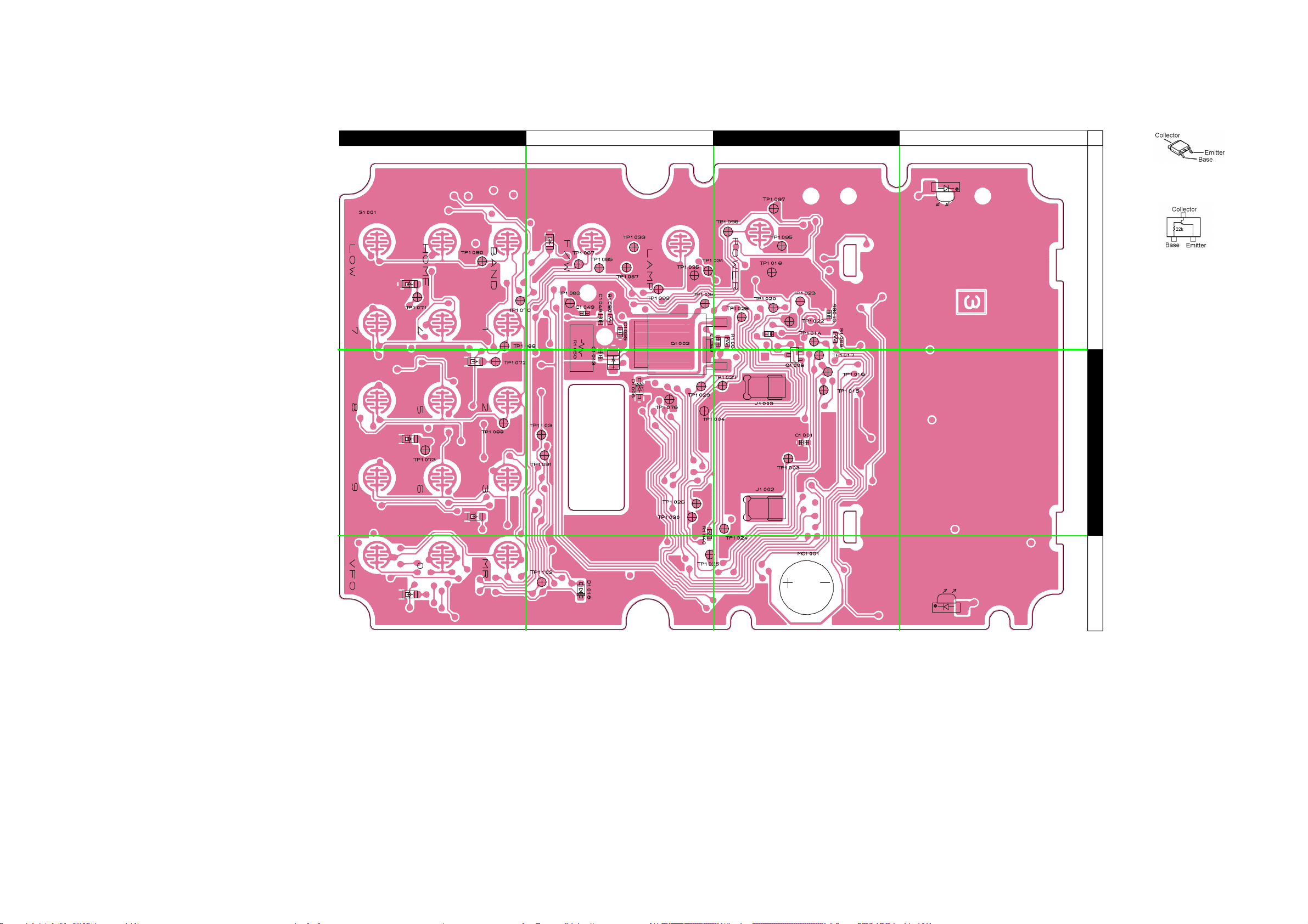
Parts Layout
CNTL Unit
A CB D
2SD1801S
(Q1002)
1
DTC124TE (05)
(Q1008)
2
3
Side A
19
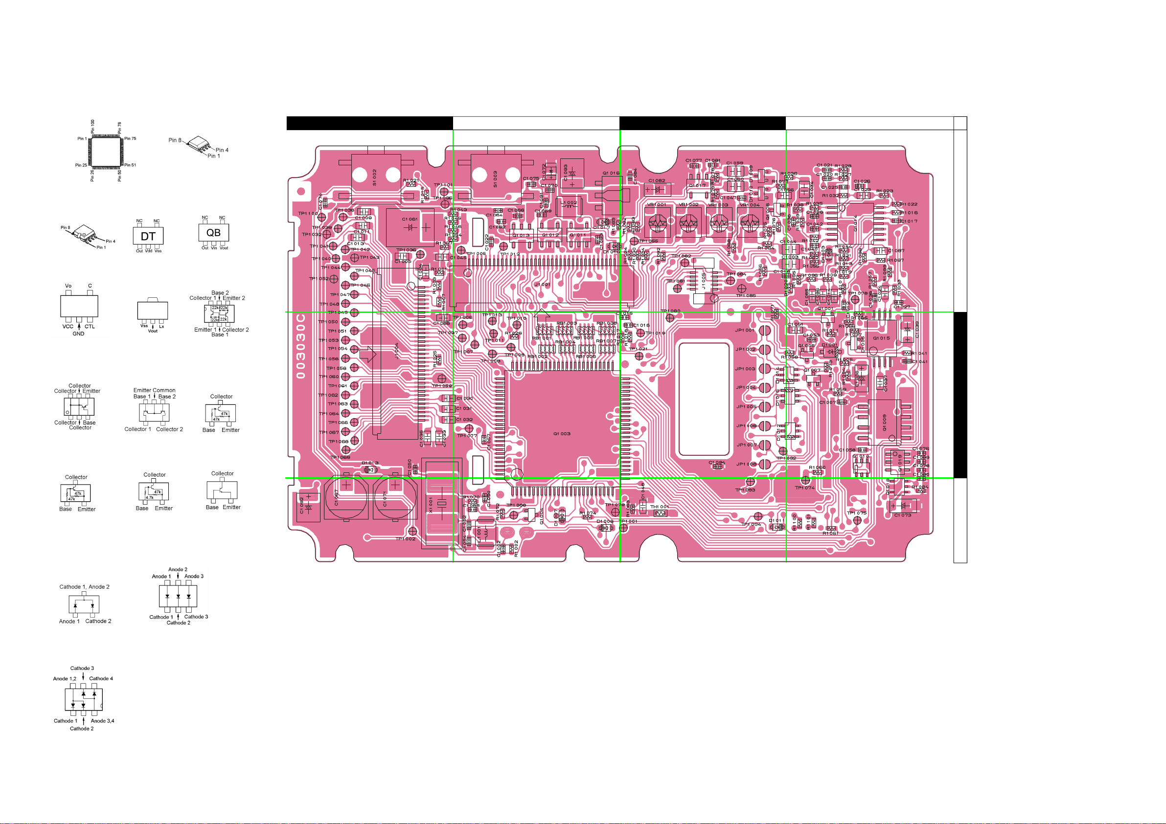
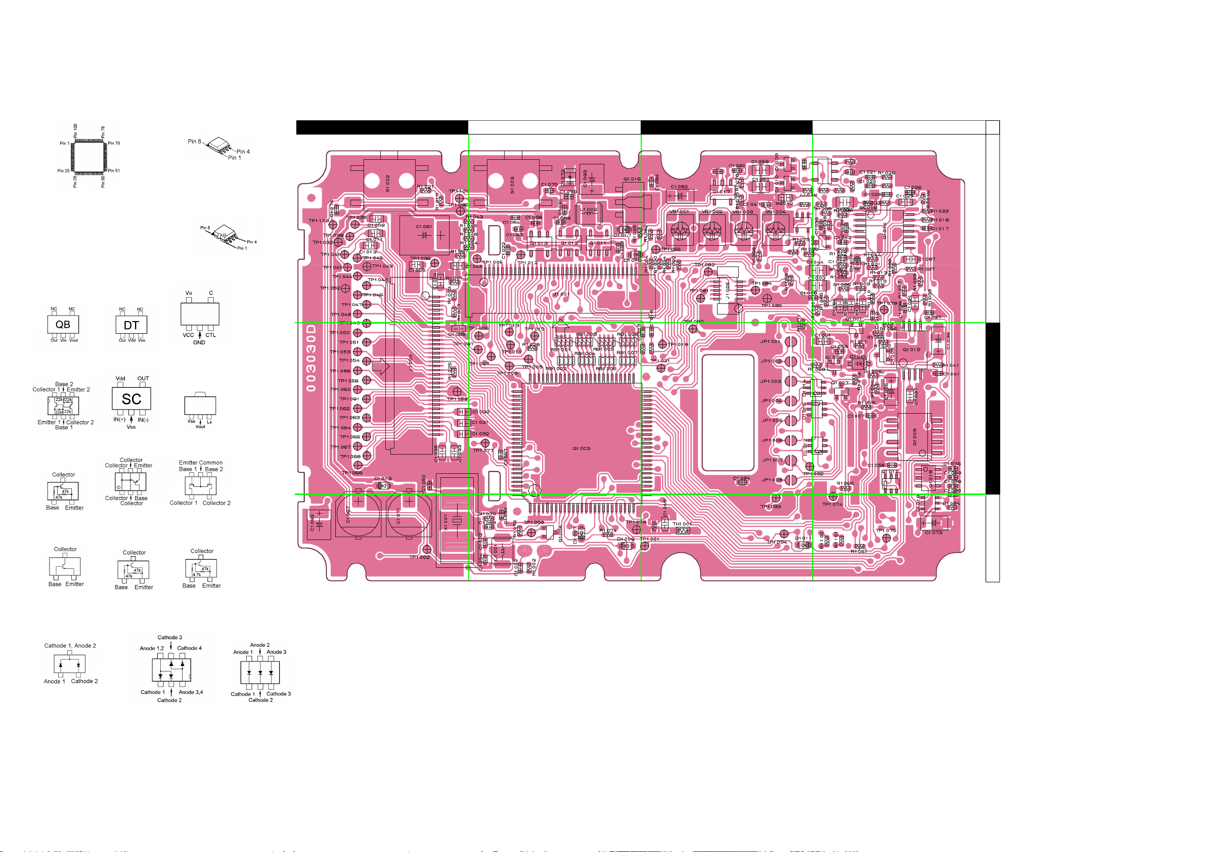
CNTL Unit
Parts Layout
HD6473877UX
(Q1003)
NJM3403AV
(Q1014)
M24C64-WMN
(Q1009)
a cb d
1
BA10358FV
(Q1015)
BA030LBSG
(Q1012)
CPH6102 (AB)
(Q1019)
DTA144EE (16)
(Q1001)
S-80730SN (DT)
(Q1011, 1017)
RH5RH651A
(Q1016)
UMW1 (W1)
(Q1018)
DTC143ZE (E23)
(Q1005)
S-81230SG (QB)
(Q1013)
UMD2N (D2)
(Q1010)
DTC144EE (26)
(Q1007)
2SC4617 (BR)
(Q1006)
2SC5374 (NA)
(Q1004)
2
3
DA221 (K)
(D1005, 1009, 1010)
UMP11N (P11)
(D1014, 1015)
20
HN2D01FU (A1)
(D1012)
Side B
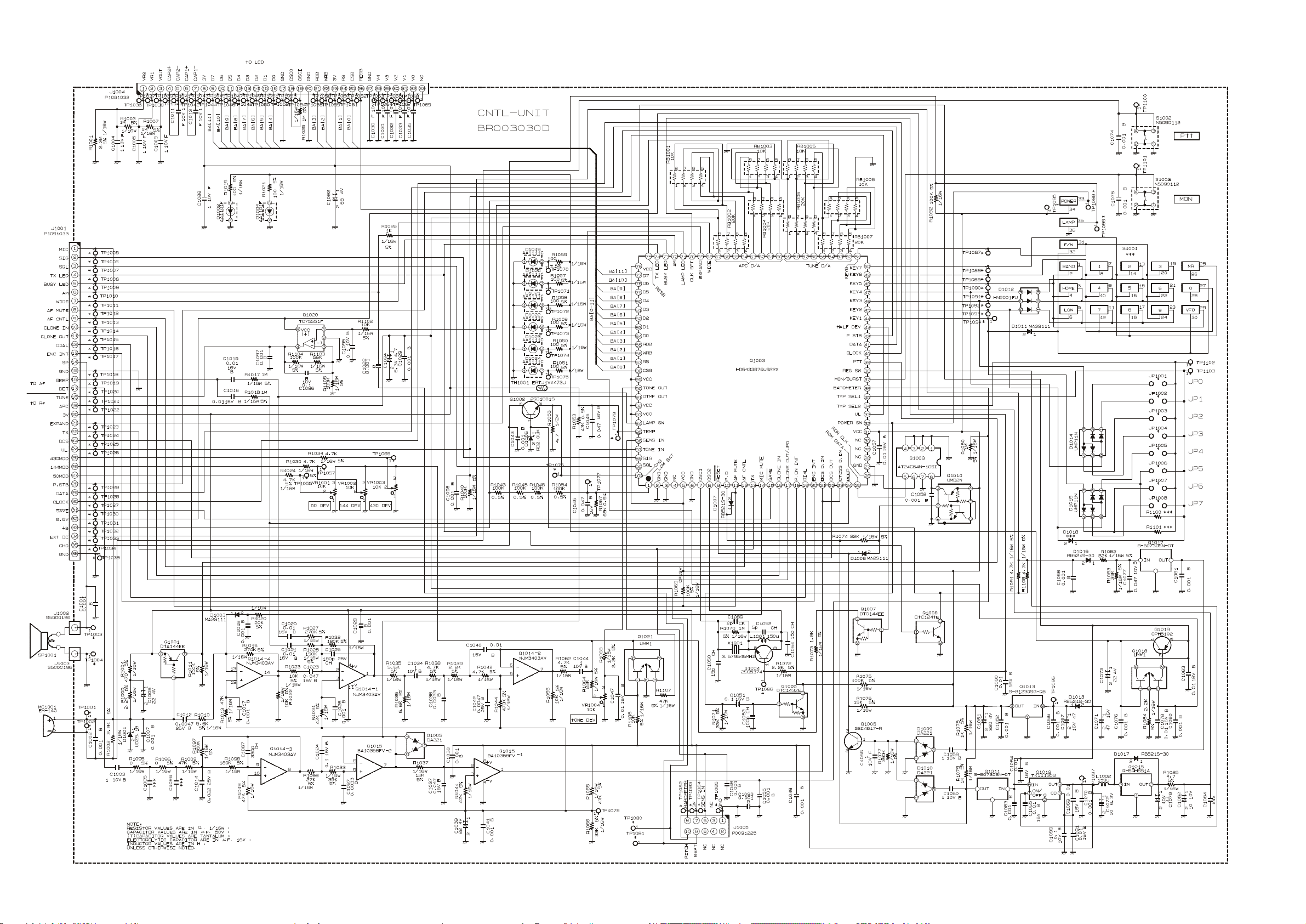
Circuit Diagram
CNTL Unit (Lot 2 ~)
21

CNTL Unit (Lot 2 ~)
Note:
22
Parts Layout
CNTL Unit (Lot 2 ~)
A CB D
2SD1801S
(Q1002)
1
DTC124TE (05)
(Q1008)
2
3
Side A
23
CNTL Unit (Lot 2 ~)
Parts Layout
NJM3403AV
(Q1014)
M24C64-WMN (Lot. 1~)
HD6473877UX (Lot. 1~)
HD6433876UB17X (Lot. 2~, USA)
HD6433876UB18X (Lot. 2~, EXP)
HD6433876UB18X (Lot. 4~, GER)
HD6433876UB25X (Lot. 6~, USA)
HD6433876UB23X (Lot. 12~, EXP, GER)
(Q1003)
AT24C64N (Lot. 18~)
(Q1009)
BA10358FV
(Q1015)
a cb d
1
S-81230SG (QB)
(Q1013)
UMD2N (D2)
(Q1010)
DTA144EE (16)
(Q1001)
2SC4617 (BR)
(Q1006)
2SC5374 (NA)
(Q1004)
S-80730SN (DT)
(Q1011, 1017)
TC75S51F (SC)
(Q1020)
CPH6102 (AB)
(Q1019)
DTC144EE (26)
(Q1007)
BA030LBSG
(Q1012)
RH5RH651A
(Q1016)
UMW1 (W1)
(Q1018, 1021)
DTC143ZE (E23)
(Q1005)
2
3
Side B
DA221 (K)
(D1005, 1009, 1010)
24
UMP11N (P11)
(D1014, 1015)
HN2D01FU (A1)
(D1012)
 Loading...