

Page 1
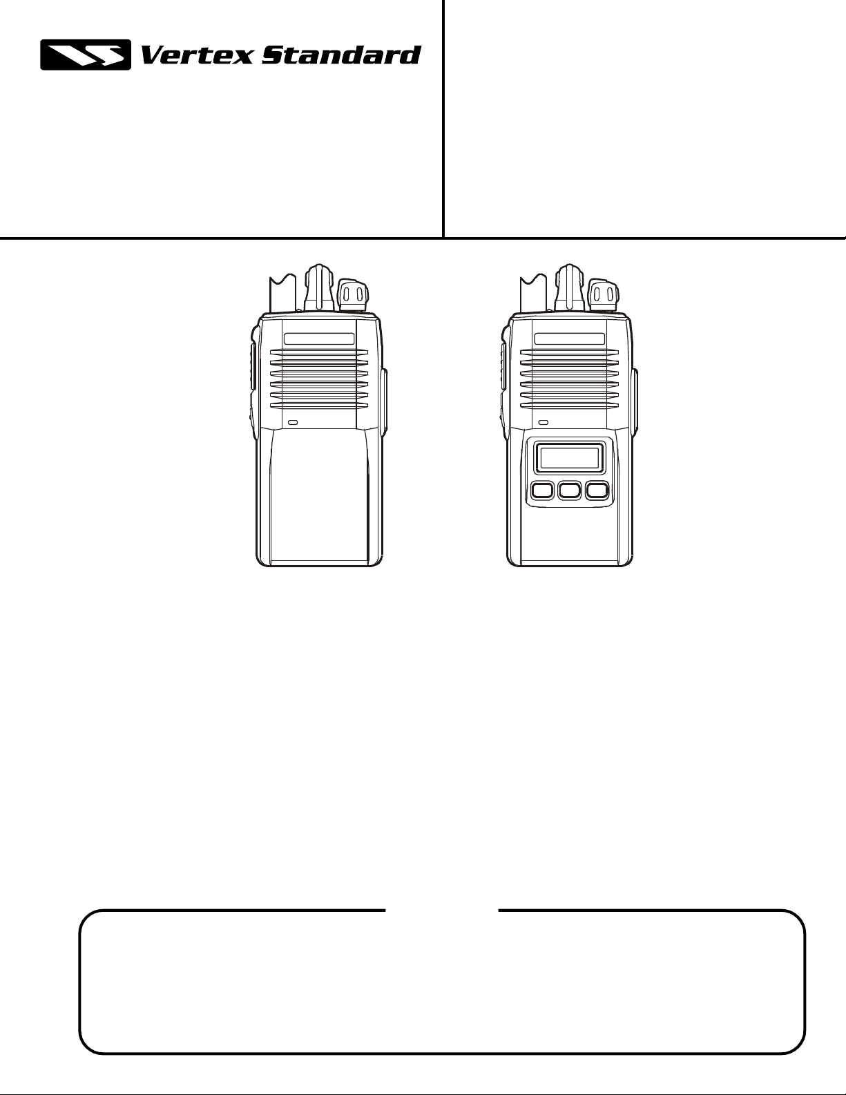
VHF FM Transceiver
VX-160V/-180V
Service Manual
©2002 VERTEX STANDARD CO., LTD. Printed in Japan.
VERTEX STANDARD CO., LTD.
4-8-8 Nakameguro, Meguro-Ku, Tokyo 153-8644, Japan
VERTEX STANDARD
US Headquarters
10900 Walker Street, Cypress, CA 90630, U.S.A.
International Division
8350 N.W. 52nd Terrace, Suite 201, Miami, FL 33166, U.S.A.
YAESU EUROPE B.V.
P.O. Box 75525, 1118 ZN Schiphol, The Netherlands
YAESU UK LTD.
Unit 12, Sun Valley Business Park, Winnall Close
Winchester, Hampshire, SO23 0LB, U.K.
VERTEX STANDARD HK LTD.
Unit 5, 20/F., Seaview Centre, 139-141 Hoi Bun Road,
Kwun Tong, Kowloon, Hong Kong
VX-160V VX-180V
Introduction
This manual provides technical information necessary for servicing the VX-160V and VX-180V FM Transceiver.
Servicing this equipment requires expertise in handling surface-mount chip components. Attempts by non-qualified
persons to service this equipment may result in permanent damage not covered by the warranty, and may be illegal in
some countries.
Two PCB layout diagrams are provided for each double-sided circuit board in the transceiver. Each side of is referred
to by the type of the majority of components installed on that side (“leaded” or “chip-only”). In most cases one side has
only chip components, and the other has either a mixture of both chip and leaded components (trimmers, coils, electrolytic capacitors, ICs, etc.), or leaded components only.
While we believe the technical information in this manual to be correct, VERTEX STANDARD assumes no liability
for damage that may occur as a result of typographical or other errors that may be present. Your cooperation in pointing
out any inconsistencies in the technical information would be appreciated.
Contents
Operating Manual Reprint ........................... 2
Cloning ............................................................. 6
Specifications................................................... 7
Exploded View & Miscellaneous Parts ...... 8
Block Diagram.................................................9
Circuit Description ................................10
Alignment ................................................12
Board Unit (
MAIN Unit............................................................... 17
Schematics, Layouts & Parts
)
1
Page 2
Operating Manual Reprint
Controls & Connectors Before You Begin
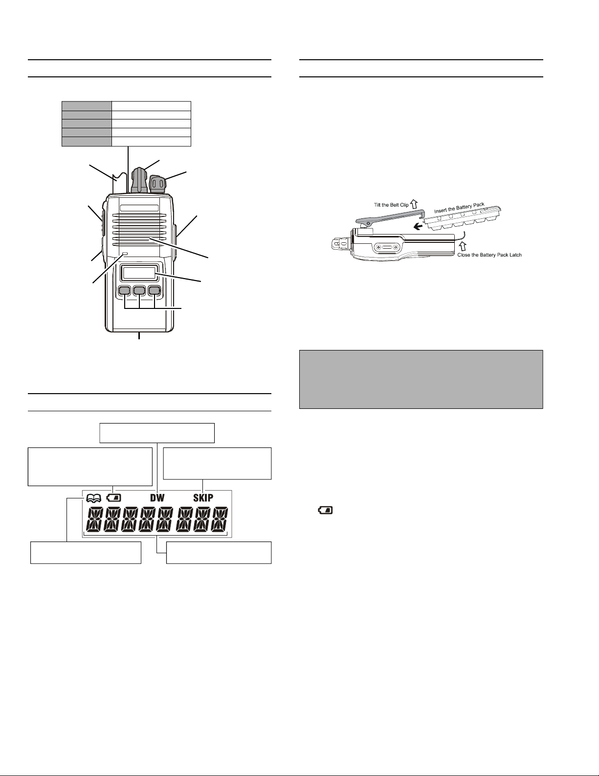
LED Indicator
Glows Green Monitor on
Blinking Green Busy Channel (or SQL off)
Glows Red Transmitting
Blinking Red Battery Voltage is low
Blinking Yellow Receiving a Selective Call
Antenna
Push To Talk
(
PTT) Switch
Monitor Button
Microphone
Battery Pack Latch
CH (Channel) Selector
VOL/PWR Knob
MIC/SP Jack
(
External Mic/Earphone
Speaker
LCD (VX-180)
Soft KEY (VX-180)
Display Icons & Indicators (VX-180 Only)
Battery Pack Installation and Removal
r To install the battery, hold the transceiver with your
left hand, so your palm is over the speaker and your
thumb is on the top of the belt clip. Insert the battery
pack into the battery compartment on the back of the
radio while tilting the Belt Clip outward, then close
the Battery Pack Latch until it locks in place with a
“Click.”
)
r To remove the battery, turn the radio off and remove
any protective cases. Open the Battery Pack latch on
the bottom of the radio, then slide the battery downward and out from the radio while holding the Belt
Clip.
Caution!
Do not attempt to open any of the rechargeable NiCd packs, as they could explode if accidentally shortcircuited.
This indicator confirms that
DUAL WATCH is active.
This icon is the “Low Battery” indicator, which appears when the
battery voltage becomes too low
for proper operation.
This indicator confirms that
DUAL 2-TONE DECODE is active.
This indicator confirms that
this channel will be skipped
during scan.
8 Character Alpha-numeric
Invertible Display
Low Battery Indication
r As the battery discharges during use, the voltage gradu-
ally becomes lower. When the battery voltage reaches
6.3 volts, substitute a freshly charged battery and recharge the depleted pack. The TX/BUSY indicator on
the top of the radio will blink red (on the VX-180, the
“ ” icon will appear on the LCD) when the battery
voltage is low.
r Avoid recharging Ni-Cd batteries often with little use
between charges, as this can degrade the charge capacity. We recommend that you carry an extra, fullycharged pack with you so the operational battery may
be used until depletion (this “deep cycling” technique
promotes better long-term battery capacity).
2
Page 3
Operation
Operating Manual Reprint
Preliminary Steps
r Install a charged battery pack onto the transceiver, as
described previously.
r Screw the supplied antenna onto the Antenna jack.
Never attempt to operate this transceiver without an
antenna connected.
r If you have a Speaker/Microphone, we recommend that
it not be connected until you are familiar with the ba-
sic operation of the VX-160/-180.
Operation Quick Start
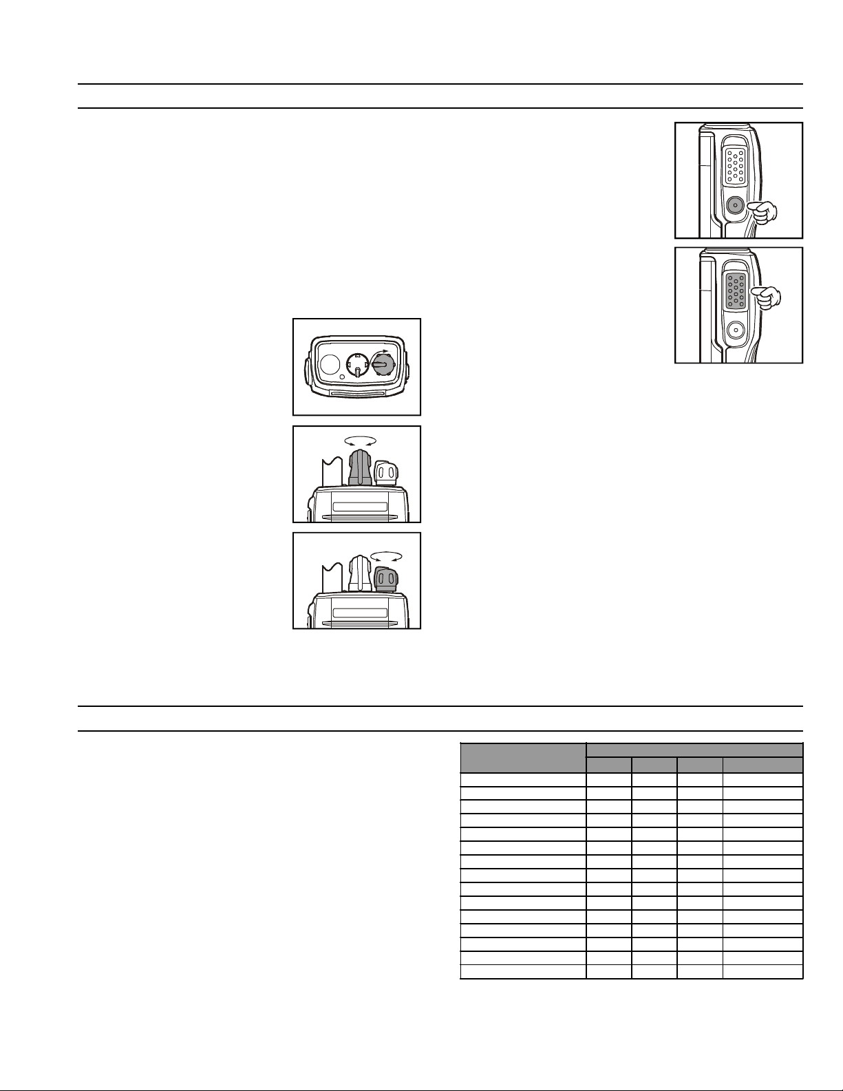
r Turn the top panel’s VOL/
PWR knob clockwise to turn
on the radio on.
r Turn the top panel’s CH selec-
tor knob to choose the desired
operating channel.
r Rotate the VOL/PWR knob to
set the volume level. If no sig-
nal is present, press and hold
in the MONITOR key (the
lower button on the left side)
for more than 1 seconds; back-
ground noise will now be heard, and you may use this
to set the VOL/PWR knob for the desired audio level.
r Press and hold in the MONI-
TOR key for more than 1 sec-
onds (or press the MONITOR
key twice) to quiet the noise
and resume normal (quiet)
monitoring.
r To transmit, press and hold in
the PTT switch. Speak into the
microphone area of the front
panel grille (lower left-hand
corner) in a normal voice level.
To return to the Receive mode,
release the PTT switch.
r If a Speaker/Microphone is available, remove the plas-
tic cap and its two mounting screws from the right side
of the transceiver, then insert the plug from the Speaker/
Microphone into the MIC/SP jack; secure the plug using the screws supplied with the Speaker/Microphone.
Hold the speaker grille up next to your ear while receiving. To transmit, press the PTT switch on the
Speaker/Microphone, just as you would on the main
transceiver’s body.
Note:Save the original plastic cap and its mounting
screws. They should be re-installed when not using the Speaker/Microphone.
Key Functions
The VX-180 provides programmable [A], [B], and [C]
function keys, and both the VX-160 and VX-180 provide
programmable MONITOR keys. These “Soft” keys functions can be customized (set to other functions), via programming by your VERTEX STANDARD dealer, to meet
your communications/network requirements. Some features may require the purchase and installation of optional
internal accessories. The possible Soft key programming
features are illustrated at the right, and their functions are
explained in the next chapter. For further details, contact
your VERTEX STANDARD dealer.
For future reference, check the box next to each function
that has been assigned to the Soft key on your particular
radio, and keep it handy.
Function
None
Monitor
Low Power
Lock*
Lamp*
Channel Up*
Channel Down*
Scan
Follow-me Scan
Dual Watch
Talk Around
Add/Del*
Call/Reset
Speed Dial
TX Save Off
* VX-180 only
Soft Key
[A] [B] [C]
MONITOR key
3
Page 4

Operating Manual Reprint
Description of Operating Functions
Monitor
Press the assigned Soft key momentarily to override (disable) the Tone squelch.
Background noise or incoming signals will now be heard
whether or not a matching tone is present on the signal).
Press and hold in the assigned Soft key for more than 1
seconds to override both the Noise and Tone squelch.
Again press and hold in the assigned Soft key for more
than 1 seconds (or press the assigned Soft key twice) to
resume normal (quiet) Noise and Tone squelch action.
Low Power
Press the assigned Soft key to set the radio's transmitter
to the “Low Power” mode, thus extending battery life.
Press the assigned Soft key again to return to “High
Power” operation when in difficult terrain.
Lock
Press the assigned Soft key to lock the Soft keys (except
Lock and Monitor key); thus, the [A], [B], [C], and MONI-
TOR keys can be disabled to prevent radio settings from
being disturbed.
Lamp
Press the assigned Soft key to illuminate the LCD for
five seconds.
Channel Up
Press the assigned Soft key to switch to a higher operating channel number.
Channel Down
Press the assigned Soft key to switch to a lower operating channel number.
Scan
The Scanning feature is used to monitor multiple channels programmed into the transceiver. While scanning, the
radio will check each channel for the presence of a signal,
and will stop on a channel if a signal is present.
r To activate scanning:
Press the assigned Soft key.
The scanner will search the channels, looking for active ones; it will pause each time it finds a channel on
which someone is speaking.
r To stop scanning:
Press the assigned Soft key.
Operation will revert to the channel to which the CH
knob is set.
Follow-Me Scan
“Follow-Me” Scan feature checks a User-assigned Priority Channel regularly as you scan the other channels. Thus,
if only Channels 1, 3, and 5 (of the 8 available channels)
are designated for “Scanning,” the user may nonetheless
assign Channel as the “User-assigned” Priority Channel
via the “Follow-Me” feature.
Press the assigned Soft key to activate “Follow-Me” scanning, then turn the CH selector knob to the channel which
you want to designate as the “User-Assigned Priority
Channel”. When the scanner stops on an “active” channel, the User-assigned Priority Channel will automatically
be checked every few seconds.
Dual Watch
The Dual Watch feature is similar to the Scan feature,
except that only two channels are monitored: the current
operating channel, and the “Priority” channel.
r To activate Dual Watch:
Press the assigned Soft key.
The scanner will search the two channels; it will pause
each time it finds a channel on which someone is speaking.
r To stop Dual Watch:
Press the assigned Soft key.
Operation will revert to the channel to which the CH
knob is set.
Talk Around
Press the assigned Soft to activate the Talk Around feature when you are operating on duplex channel systems
(separate receive and transmit frequencies, utilizing a “repeater” station). The Talk Around feature allows you to
bypass the repeater station and talk directly to a station
that is nearby. This feature has no effect when you are
operating on “Simplex” channels, where the receive and
transmit frequencies are already the same.
Note that your dealer may have made provision for “Talk
Around” channels by programming “repeater” and “Talk
Around” frequencies on two adjacent channels. If so, the
key may be used for one of the other Pre-Programmed
Functions.
Add/Del
The Add/Del feature allows the user to arrange a custom
Scan.
Press the assigned Soft key to delete/restore the current
channel to/from your scanning list.
When you delete a current channel, “SKIP” will appear
on the LCD after pressing the Soft key. When you restore a current channel, “SKIP” indicator on the LCD
will turn off.
4
Page 5

Operating Manual Reprint
Description of Operating Functions
Call/Reset
When the 2-tone selective calling unit is installed, press
the assigned Soft key to silence the receiver and reset for
another call, when a communication is finished.
Speed Dial
Your Dealer may have pre-programmed Auto-Dial telephone number memories into your radio.
To dial a number, just press the Dealer-assigned Soft key
for Speed Dialing. The DTMF tones sent during the dialing sequence will be heard in the speaker.
Accessories & Options
FNB-64 7.2 V 700 mAh Ni-Cd Battery
FNB-V57 7.2 V 1100 mAh Ni-Cd Battery
FBA-25 Alkaline Battery Case
NC-77B 120 VAC Overnight Desktop Charger
NC-77C 230-240 VAC Overnight Desktop Charger
VAC-800 Desktop Rapid Charger
VAC-6800 6-unit Multi Charger
MH-45B4B Speaker/Microphone
MH-37A4B Earpiece Microphone
VC-25 VOX Headset
VCM-1 Mobile Mounting Bracket (for VAC-800)
LCC-160/S Leather Case (for VX-160)
LCC-180/S Leather Case (for VX-180)
CT-42 PC Programming Cable
CT-27 Radio to Radio Programming Cable
CE44 Programming Software
TX Save Off
Press the assigned Soft key to disable the Transmit Battery Saver, if you are operating in a location where high
power is almost always needed.
The Transmit Battery Saver helps extend battery life by
reducing transmit power when a very strong signal from
an apparently nearby station is being received. Under some
circumstances, though, your hand-held radio may not be
heard well at the other end of the communication path,
and high power may be necessary at all times.
5
Page 6
Cloning
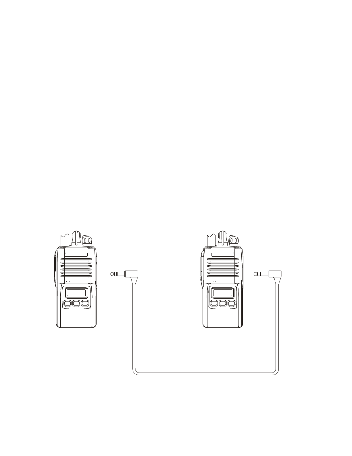
The VX-160/-180 includes a convenient “Cloning” feature, which allows the programming data from one transceiver to
be transferred to another VX-160/-180. Here is the procedure for Cloning one radio's data to another.
1. Turn both transceivers off.
2. Remove the plastic cap and its two mounting screws
from the MIC/SP jack on the right side of the transceiver. Do this for both transceivers.
3. Connect the optional CT-27 cloning cable between the
MIC/SP jacks of the two transceivers.
4. Press and hold in the PTT and MONITOR switches
(just below the PTT switch) while turning the transceiver on. Do this for both transceivers (the order of
the switch-on does not matter). “CLONE” will appear
on the displays (for the VX-180) of both transceivers
when Clone mode is successfully activated in this step;
in the case of the VX-160, no change will be observed
at this point.
5. On the Destination transceiver, press the MONITOR
switch. “LOADING” will appear on the LCD (for VX-
180; for VX-160, the TX/BUSY indicator on the top
of the radio will glow Green).
6. Press the PTT switch on the source transceiver; “SEND-
ING” will appear on the Source transceiver (for VX180; for VX-160, the TX/BUSY indicator on the top
of the radio will glow Red), and the data will be transferred.
7. If there is a problem during the cloning process, “ER-
ROR” will appear on the LCD (for VX-180; for VX-
160, the TX/BUSY indicator on the top of the radio
will blink Red); check your cable connections and battery voltage, and try again.
8. If the data transfer is successful, the display will re-
turn to “CLONE” (for VX-180; for VX-160, the TX/
BUSY indicator on the top of the radio will turn off).
Turn both transceivers off and disconnect the CT-27
cable. You can then turn the transceivers back on, and
begin normal operation.
9. Replace the plastic cap and its two mounting screws.
Optional Cloning Cable CT-27
6
Page 7

Specifications
GENERAL Specifications
Frequency Range (MHz): 134 - 160 (A)
148 - 174 (C)
Number of Channels: 16 channels
Channel Spacing: 12.5 / 25 kHz (15 / 30 kHz)
PLL Steps 2.5 / 6.25 kHz
Power Supply voltage: 7.5 VDC ± 20%
Operating Temperature Range: –22°F to +140°F (–30°C to +60°C)
Frequency Stability: ±2.5 ppm
Dimensions (WHD): 2.3" (W) x 4.7" (H) x 1.2" (D) (58 x 120 x 31 mm)
Weight (approx.): 0.81 lb. (365 g) w/FNB-64
RECEIVER Specifications (Measurements made per EIA standard TIA/EIA-603)
Sensitivity
EIA 12 dB SINAD : 0.20 µV
20 dB Quieting : 0.30 µV
Adjacent channel selectivity: 65 dB (25 kHz) / 60 dB (12.5 kHz)
Intermodulation: 65 dB
Spurious and Image Rejection: 65 dB
Hum & Noise 45 dB
Audio output: 500 mW @4 Ohms, 5% THD
TRANSMITTER Specifications (Measurements made per EIA standard TIA/EIA-603)
Power output: 5.0 / 1.0 W
Modulation: 16K0F3E, 11K0F3E
Conducted Spurious Emissions: 60 dB Below Carrier
FM Hum & Noise: 40 dB (25 kHz) / 35 dB (12.5 kHz)
Audio distortion (@ 1 kHz): < 5 %
Measurements per EIA standards unless noted above. Specifications subject to change without notice or obligation.
7
Page 8
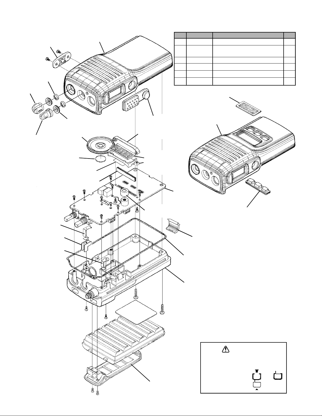
Exploded View & Miscellaneous Parts
RA029600A (Lot. 17~)
RA0173500
CAP
Â
R6147510
RING NUT (x 2 pcs)
RA0296100
VOLUME KNOB
RA029620A (Lot. 3~)
RA0296200 (Lot. 1~)
KNOB (CH)
RA0309800 (Lot. 20~)
MYLAR SHEET (SP)
RA0334900A
REFLECTOR SHEET (VX-180)
RA0294800
INTER CONNECTOR (VX-180)
RA0107000
TERMINAL PLATE R
RA010340A
TERMINAL HOLDER
RA0296000 (Lot. 1~)
FRONT CASE ASSY (VX-160)
Â
RA0210600
RUBBER PACKING (x 2 pcs)
M4090151A (Lot. 10~)
M4090151 (Lot. 1~)
SPEAKER
À
À
À
À
À
Á
À
À
À
RA0294200
PTT KNOB
RA0294400
LCD HOLDER (VX-180)
G6090139
LCD (VX-180)
RA029450A (Lot. 10~)
RA0294500
LIGHT GUIDE (VX-180)
À
RA0110200
Á
HOLDER RUBBER
REF. VXSTD P/N Description Qty.
MAIN Unit
À U44104002 TAPTITE SCREW M2X4NI 10
U44104002
Á
(VX-180U)
TAPTITE SCREW M2X4NI 2
 U20206007 BINDING HEAD SCREW M2.6X6B 2
à U24110002 TAPTITE SCREW M2X10NI 2
Ä U02206007 SEMS SCREW SM2.6X6B 2
Å U00103002 PAN HEAD SCREW M2X3NI 1
RA0210900
WINDOW
RA029590B (Lot. 17~)
RA0295900 (Lot. 1~)
FRONT CASE ASSY (VX-180)
RA0293900
RUBBER KNOB
RA0123500
LATCH NAIL B
TERMINAL PLATE L
À
Ä
Ä
Å
Ã
CP7064001
BELT CLIP ASSY
Ã
RA0294300 (Lot. 1~)
RA029430A (Lot. 4~)
RUBBER PACKING
RA029310D (Lot. 26~)
RA029310C (Lot. 20~)
RA029310B (Lot. 11~)
RA029310A (Lot. 3~)
RA0293100
REAR CASE ASSY
(w/SMA CONNECTOR, TERMINAL PLATE L,
PAN HEAD SCREW M2X3NI)
CAUTION
The mic element must be desoldered
and removed from the PCB on order to reinstall its protective rubber cover.
Therefore, be
careful not to remove
this cover unless mic
element replacement
is necessary.
ÁÀ
8
Page 9
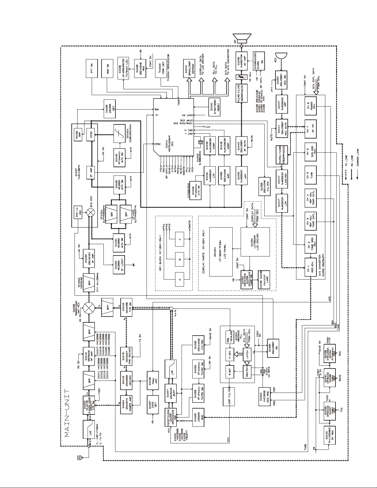
Block Diagram
9
Page 10

Circuit Description
Receive Signal Path
Incoming RF from the antenna jack is delivered to the
RF Unit and passes through a low-pass filter consisting
of coils L1001, L1002, and L1031, capacitors C1004,
C1005, C1008, C1010, C1014, C1016, and C1221, and
antenna switching diode D1003 (RLS135 TE-17).
Signals within the frequency range of the transceiver
enter a varactor-tuned band-pass filter consisting of coils
L1010 and L1011, capacitors C1044, C1046, C1060,
C1065, and C1068, and diodes D1011 (HVC358B),
D1012 (HVC358B), D1013 (HVC358B), and D1014
(HVC358B), then are amplified by Q1012 (2SC5006-
T1) and enter a varactor-tuned band-pass filter consisting
of coils L1017 and L1021, capacitors C1084, C1086,
C1095, and C1097, and diodes D1018 (HVC358B) and
D1019 (HVC358B), before mixing by first mixer Q1026
(SGM2016AM-T7).
Buffered output from the VCO is amplified by Q1007
(2SC5005-T1) to provide a pure first local signal between 190.25 and 218.25 MHz for injection to the first
mixer. The 44.25 MHz first mixer product then passes
through monolithic crystal filter XF1002 (HDF0042, 5.5
kHz BW) to strip away unwanted mixer products, and the
IF signal is then amplified by Q1033 (2SC4215Y
TE85R).
The amplified first IF signal is applied to FM IF subsystem IC Q1037 (TA31136FN-EL), which contains the
second mixer, second local oscillator, limiter amplifier,
noise amplifier, and RSSI amplifier.
The second local signal is produced from the PLL reference/second local oscillator of 14.60 MHz crystal
X1001. The 14.60 MHz reference signal is tripled by
Q1036, capacitor C1209, and coil L1029, and the resulting 43.8 MHz second local signal is then delivered to the
mixer section of Q1037, which produces the 450 kHz second IF when mixed with the first IF signal.
The second IF then passes through ceramic filter
CF1001 (ALFYM450G=K on “Narrow” channels) or
CF1002 (ALFYM450F=K on “Wide” channels) to strip
away all but the desired signal, and then is applied to the
limiter amplifier in Q1037, which removes amplitude
variations in the 450 kHz IF, before detection of the speech
by the ceramic discriminator, CD1001 (CDBC450CX24).
Detected audio from Q1037 is applied to the audio
high-pass filter, and then passes via the volume control to
the audio amplifier Q1039 (NJM2070M-TE2), which
provides up to 1/2 Watt to the optional headphone jack or
a 4-ohm loudspeaker.
10
Squelch Control
The squelch circuitry consists of a noise amplifier and
band-pass filter within Q1037, and noise detector D1018
(1SS355 TE-17).
When no carrier is received, noise at the output of the
detector stage in Q1037 is amplified and band-pass filtered by the noise amplifier section of Q1037 and the network between pins 7 and 8, and then is rectified by D1028.
The resulting DC squelch control voltage is passed to
pin 37 of the microprocessor Q1014 (M37516E6HP). If
no carrier is received, this signal causes pin 24 of Q1014
to go high and pin 20 to go high. Pin 24 signals Q1060
(RT1P441U-T11-1) to disable the supply voltage to the
audio amplifier Q1039, while pin 20 holds the green
(Busy) half of the LED off, when pin 24 is high and pin
20 is high.
Thus, the microprocessor blocks output from the audio amplifier, and silences the receiver, while no signal is
being received (and during transmission, as well).
When a carrier appears at the discriminator, noise is
removed from the output, causing pin 37 of Q1014 to go
low and the microprocessor to activate the “Busy” LED
via Q1014.
The microprocessor then checks for CTCSS or CDCSS
code squelch information, if enabled. If not transmitting
and CTCSS or CDCSS is not activated, or if the received
tone or code matches that programmed, audio is allowed
to pass through the audio amplifier Q1039 (NJM2070M
TE2) to the loudspeaker by the enabling of the supply
voltage to it via Q1037.
Transmit Signal Path
Speech input from the microphone is amplified by
Q1017 (NJM2902V TE1);
and R1054, the audio is amplified in another section of Q1017.
The processed audio may then be mixed with a CTCSS
tone generated by Q1014 (M37516E6HP) for frequency
modulation of the PLL carrier (up to ±5 kHz from the
unmodulated carrier) at the transmitting frequency.
If a CDCSS code is enabled for transmission, the code
is generated by microprocessor Q1014 (M37516E6HP)
and delivered to D1004 (HVC350B TRF) for CDCSS
modulating.
The modulated signal from the VCO Q1002
(2SC5231C8-TL) is buffered by Q1007 (2SC5005-T1).
The low-level transmit signal then passes through the T/
R switching diode D1016 (DAN235E-TL) to driver amplifiers Q1015 (2SC5227-4-TB) and Q1016
(2SK2596BXTL), then the amplified transmit signal is
applied to the final amplifier Q1024 (2SK2974-T11),
which delivers up to 5 watts of output power.
The transmit signal then passes through the antenna
switch D1003 (RLS135 TE-11) and is low-pass filtered,
to suppress harmonic spurious radiation, before delivery
to the antenna.
after pre-emphasis by C1066
Page 11

Circuit Description
Automatic Transmit Power Control
Current from the final amplifier is sampled by R1108,
R1115, and R1125, and is rectified by Q1057 (IMZ2A
T108). The resulting DC is fed back through Q1032
(FMW1 T98) to the drive amplifier Q1016 and final amplifier Q1024, for control of the power output.
The microprocessor selects “High” or “Low” power levels.
Transmit Inhibit
When the transmit PLL is unlocked, pin 7 of PLL chip
Q1005 goes to a logic “Low,” and unlock detector Q1056
(2SA1586Y TE85R) goes to a logic “High.” The resulting DC unlock control voltage is passed to pin 14 of the
microprocessor, Q1014. While the transmit PLL is unlocked, pin 22 of Q1014 remains high, which then turns
off Q1029 (CPH6102-TL) and the Automatic Power Controller Q1032 (FMW1 T98) to disable the supply voltage
to the drive amplifiers Q1015/Q1016 and final amplifier
Q1024, thereby disabling the transmitter.
Spurious Suppression
Generation of spurious products by the transmitter is
minimized by the fundamental carrier frequency being
equal to final transmitting frequency, modulated directly
in the transmit VCO. Additional harmonic suppression is
provided by a low-pass filter consisting of coils L1001,
L1002, and L1031 plus capacitors C1004, C1005, C1008,
C1010, C1014, C1016, and C1221, resulting in more than
60 dB of harmonic suppression prior to delivery of the
RF signal to the antenna.
PLL Frequency Synthesizer
The PLL circuitry on the Main Unit consists of VCO
Q1002 (2SC5231C8-TL), VCO buffer Q1007
(2SC5005), and PLL subsystem IC Q1005
(MB15A02PFV1-G-BND-EF), which contains a reference divider, serial-to-parallel data latch, programmable
divider, phase comparator, and charge pump.
Frequency stability is maintained by temperature compensating thermistor TH1004. The output from TH1004
is applied to pin 39 of Q1014. Q1014 outputs thermal
data to D/A converter Q1052 (M62364FP 600D), which
produces a DC voltage corresponding to the thermal data.
The resulting DC voltage is applied to varactor diode
D1004 (HVC350B TRF) to stabilize the 14.60 MHz Reference Frequency.
While receiving, VCO Q1002 oscillates between
190.25 and 218.25 MHz according to the transceiver version and the programmed receiving frequency. The VCO
output is buffered by Q1007, then applied to the prescaler
section of Q1005. There the VCO signal is divided by 64
or 65, according to a control signal from the data latch
section of Q1005, before being sent to the programmable
divider section of Q1005.
The data latch section of Q1005 also receives serial
dividing data from the microprocessor, Q1014, which
causes the pre-divided VCO signal to be further divided
in the programmable divider section, depending upon the
desired receive frequency, so as to produce a 2.5 kHz or
3.125 kHz derivative of the current VCO frequency.
Meanwhile, the reference divider section of Q1005
divides the 14.60 MHz crystal reference (from the reference oscillator, Q1022) by 5840 (or 4672) to produce the
2.5 kHz (or 3.125 kHz) loop references (respectively).
The 2.5 kHz (or 3.125 kHz) signal from the programmable divider (derived from the VCO) and that derived
from the reference oscillator are applied to the phase detector section of Q1004, which produces a pulsed output
with pulse duration depending on the phase difference
between the input signals.
This pulse train is filtered to DC and returned to the
varactor D1037 (HVC358B) and D1042 (HVC355B).
Changes in the level of the DC voltage are applied to the
varactor, affecting the reference in the tank circuit of the
VCO according to the phase difference between the signals derived from the VCO and the crystal reference oscillator.
The VCO is thus phase-locked to the crystal reference
oscillator. The output of the VCO Q1002, after buffering
by Q1007, is applied to the first mixer as described previously.
For transmission, the VCO Q1002 oscillates between
146 and 174 MHz according to the model version and
programmed transmit frequency. The remainder of the PLL
circuitry is shared with the receiver. However, the dividing data from the microprocessor is such that the VCO
frequency is at the actual transmit frequency (rather than
offset for IFs, as in the receiving case). Also, the VCO is
modulated by the speech audio applied to D1005 (1SV229
TPH3), as described previously.
Receive and transmit buses select which VCO is made
active, using Q1059 (RT1N441U-T11-1) and Q1059
(RT1P441U-T11-1).
Miscellaneous Circuits
Push-To-Talk Transmit Activation
The PTT switch on the microphone is connected to
pin 48 of microprocessor Q1014, so that when the PTT
switch is closed, pin 23 of Q1014 goes low. This signal
disables the receiver by disabling the 5 V supply bus at
Q1036 (DTB123EK T146) to the front-end, FM IF subsystem IC Q1037, and the receiver VCO circuitry.
At the same time, Q1027 (FMW1 T98) and Q1029
(CPH6102-TL) activate the transmit 5V supply line to
enable the transmitter.
11
Page 12

Alignment
Introduction
The VX-160/-180 has been aligned at the factory for
the specified performance across the entire frequency
range specified. Realignment should therefore not be necessary except in the event of a component failure. All component replacement and service should be performed only
by an authorized Vertex Standard representative, or the
warranty policy may be voided.
The following procedures cover the sometimes critical and tedious adjustments that are not normally required
once the transceiver has left the factory. However, if damage occurs and some parts are replaced, realignment may
be required. If a sudden problem occurs during normal
operation, it is likely due to component failure; realignment should not be done until after the faulty component
has been replaced.
We recommend that servicing be performed only by
authorized Vertex Standard service technicians who are
experienced with the circuitry and fully equipped for repair and alignment. Therefore, if a fault is suspected, contact the dealer from whom the transceiver was purchased
for instructions regarding repair. Authorized Vertex Standard service technicians realign all circuits and make complete performance checks to ensure compliance with factory specifications after replacing any faulty components.
Those who do undertake any of the following alignments
are cautioned to proceed at their own risk. Problems caused
by unauthorized attempts at realignment are not covered
by the warranty policy. Also, Vertex Standard must reserve the right to change circuits and alignment procedures in the interest of improved performance, without
notifying owners. Under no circumstances should any
alignment be attempted unless the normal function and
operation of the transceiver are clearly understood, the
cause of the malfunction has been clearly pinpointed and
any faulty components replaced, and the need for realignment determined to be absolutely necessary. The following test equipment (and thorough familiarity with its correct use) is necessary for complete realignment. Correction of problems caused by misalignment resulting from
use of improper test equipment is not covered under the
warranty policy. While most steps do not require all of
the equipment listed, the interactions of some adjustments
may require that more complex adjustments be performed
afterwards. Do not attempt to perform only a single step
unless it is clearly isolated electrically from all other steps.
Have all test equipment ready before beginning, and follow all of the steps in a section in the order presented.
Required Test Equipment
r Avionics Radio Tester with calibrated output level at
500 MHz
r In-line Wattmeter with 5% accuracy at 500 MHz
r 50-ohm, 10-W RF Dummy Load
r Regulated DC Power Supply (standard 7.5V DC, 2A)
r Frequency Counter: ±0.2 ppm accuracy at 500 MHz
r AF Signal Generator
r AC Voltmeter
r DC Voltmeter
r UHF Sampling Coupler
r IBM PC/compatible Computer with Microsoft DOS
v3.0 or later operating system
r Vertex Standard CT-42 Connection Cable and CE44
Alignment program
Alignment Preparation & Precautions
A 50-ohm RF Dummy load and in-line wattmeter must
be connected to the main antenna jack in all procedures
that call for transmission, except where specified otherwise. Correct alignment is not possible with an antenna.
After completing one step, read the following step to
determine whether the same test equipment will be required. If not, remove the test equipment (except dummy
load and wattmeter, if connected) before proceeding.
Correct alignment requires that the ambient temperature be the same as that of the transceiver and test equipment, and that this temperature be held constant between
20° and 30°C (68°~ 86°F). When the transceiver is brought
into the shop from hot or cold air, it should be allowed
time to come to room temperature before alignment.
Whenever possible, alignments should be made with
oscillator shields and circuit boards firmly affixed in place.
Also, the test equipment must be thoroughly warmed up
before beginning.
Note:Signal levels in dB referred to in this procedure are
based on 0 dBµ = 0.5 µV (closed circuit).
Important Note
When connecting the CT-42 plug into the MIC/SP
jack of the VX-160/-180, you must remove the plastic cap and its mounting screws prior to programming.
Please remember to re-attach the cap and screws when
the programming is complete.
12
Page 13
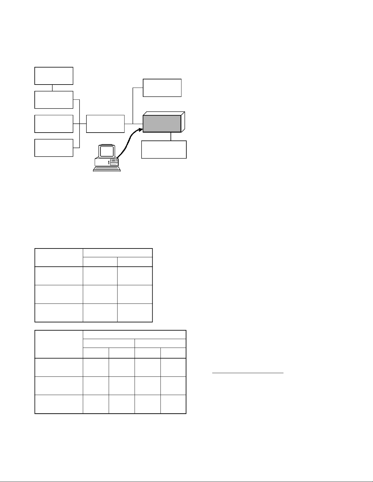
Alignment
Set up the test equipment as shown below for transceiver alignment, and apply 7.5V DC power to the transceiver.
50-ohm
Dummy Load
RF Signal
Generator
Inline Wattmeter
Deviation Meter
Frequency
Counter
RF Sampling
Coupler
CT-42 connection
Cable
PC
COM port
Transceiver
MIC/SP
Power Supply
7.5V DC
The transceiver must be programmed for use in the
intended system before alignment is attempted. The RF
parameters are loaded from the file during the alignment
process.
In order to facilitate alignment over the complete operating rang of the equipment, it is recommended that the
channel data in the transceiver be preset as per the chart
below.
Channels
Low Band Edge 134.000 148.000
(Channel 1) (Low POWER) (Low POWER)
Band Center 147.000 161.000
(Channel 2) (High POWER)(High POWER)
High Band Edge 160.000 174.000
(Channel 3) (High POWER)(High POWER)
Channel
Low Band Edge
(Channel 1)
Band Center
(Channel 2)
High Band Edge
(Channel 3)
Frequency (MHz)
Ver. A Ver. C
Tone-Frequency (Hz) / DCS-code
Ver. A Ver. C
CTCSS DCS CTCSS DCS
– – – –
151.4 – 151.4 –
– 627 – 627
The alignment tool outline
Installation of the Alignment tool
The “alignment mode” is a software-based protocol,
accessed by an “Alignment Mode” command from the
computer while switching the transceiver on.It is operated by the alignment tool automatically. During use of
the alignment mode, normal operation is suspended. The
alignment tool program provides all needed operation capability.
The alignment tool consists of an executable file
“CE44.exe” and an accmpanying configuration file
“CE44.cfg” which should be loaded per standard DOS
procedures. Create a suitable directory, then copy these
foles from the distribution diskette into the new directory.
For example, if copying the file from Drive A, use the
following DOS command sequence:
c:\ mkdir align [enter]
c:\ cd align [enter]
c:\ align\ copy a:ce44.*
No further installation steps are required. If you wish
to utilize a different name for the alignment directory, it
will not matter to the executable file.
Booting the Alignment Tool
Change to the “align” directory (or the directory name
you utilized in the previous section). Now type on the
command line: ce44 [ENTER] to boot the alignment tool.
The introductory screen will appear, and you may press
any key to enter the main screen.
Entering Alignment Mode
To enter the alignment mode, turn the transceiver off,
Select “Radio” then “Adjust” parameter. Now, turn the
transceiver back on. When the command has been successful, a message on the computer screen will confirm
that the transceiver is now in the “Alignment” mode.
Alignment Sequence
Although the data displayed on the computer's screen
during alignment is temporary data, it is important you
follow the basic alignment sequence precisely, so that the
displayed data and the data loaded into the transceiver are
identical.
Basic Alignment Sequence
1. Enter the alignment mode
2. Upload data from transceiver
3. Align data
4. Download data to transceiver
13
Page 14

Alignment
PLL VCV (Varactor Control Voltage)
r Connect the DC voltmeter between TP3 on the Main
Unit and ground.
r Set the transceiver to CH 3 (high band edge), and ad-
just L1004 on the Main Unit for 3.7~3.8 V on the DC
voltmeter.
r Set the transceiver to CH 1 (low band edge), and con-
firm the low-end VCV is 0.9 ~ 1.5 V while transmitting, and also while receiving.
Transmitter Output Power
High Power
r Set the transceiver to CH 2 (band center).
r Open the “Adjust” window on the CE44 program, then
select the “RF Power (High)” parameter.
r Press the [ENTER] key to enable programming of this
parameter; use the
power meter reading is 5.5 W (± 0.1 W). Confirm that
the current consumption is 2.2 A or lower.
r Press the [ENTER] key to lock in the new data.
Low Power
r Set the transceiver to CH 1 (Low band edge).
r Open the “Adjust” window on the CE44 program, then
select the “RF Power (Low)” parameter.
r Press the [ENTER] key to enable programming of this
parameter; use the
power meter reading is 1.0 W (± 0.1 W) (for “RF Power
Low”). Confirm that the current consumption is 1.0 A
or lower.
r Press the [ENTER] key to lock in the new data.
[¡]
[¡]
or
or
[¢]
arrow keys so that the
[¢]
arrow keys so that the
MIC Sensitivity
r Set the transceiver to CH 2 (band center).
r Inject a 1 kHz tone at –37 dBm to the MIC jack.
CLONE GND
SP
IN
r Open the “Adjust” window on CE44, then select the
“MIC Sensitivity” parameter.
r Press the [ENTER] key to enable programming of this
parameter; use the
deviation meter reading is ±3.0 kHz (±0.1 kHz) (for
25 kHz steps) deviation.
r Press the [ENTER] key to lock in the new data.
[¡]
or
[¢]
arrow keys so that the
14
L1004TP3
Page 15

Alignment
MAX Deviation
r Set the transceiver to CH 2 (band center).
r Inject a 1 kHz tone at –17 dBm to the MIC jack.
r Open the “Adjust” window on CE44, then select the
“MAX Deviation” parameter.
r Press the [ENTER] key to enable programming of this
parameter; use the
deviation meter reading is ±4.2 kHz (±0.1 kHz) (for
25 kHz steps) or ±2.1 kHz (±0.1 kHz) (for 12.5 kHz
steps) deviation.
r Press the [ENTER] key to lock in the new data.
[¡]
or
[¢]
arrow keys so that the
CTCSS Deviation
r Set the transceiver to CH 2 (band center).
r Open the “Adjust” window on CE44, then select the
“CTCSS Deviation” parameter.
r Press the [ENTER] key to enable programming of this
parameter; use the
deviation meter reading is ±0.8 kHz (±0.1 kHz) (for
25 kHz steps) or ±0.5 kHz (±0.1 kHz) (for 12.5 kHz
steps) deviation.
r Press the [ENTER] key to lock in the new data.
[¡]
or
[¢]
arrow keys so that the
DCS Deviation
r Set the transceiver to CH 3 (high band edge).
r Open the “Adjust” window on CE44, then select the
“DCS Deviation” parameter.
r Press the [ENTER] key to enable programming of this
parameter; use the
deviation meter reading is ±0.75 kHz (±0.1 kHz) (for
25 kHz steps) or ±0.35 kHz (±0.1 kHz) (for 12.5 kHz
steps) deviation.
r Press the [ENTER] key to lock in the new data.
[¡]
or
[¢]
arrow keys so that the
RF Frequency
r Set the transceiver to CH 2 (band center).
r Open the “Adjust” window on CE44, then select the
“RF Frequency” parameter.
r Press the [ENTER] key to enable programming of this
parameter; use the
frequency counter displays the band center frequency
(±100 Hz) for the version being aligned.
r Press the [ENTER] key to lock in the new data.
[¡]
or
[¢]
arrow keys so that the
Sensitivity
r Set the transceiver to CH 3 (high band edge).
r Tune the RF signal generator to the same frequency as
the transceiver’s, then set the generator output level to
40 dBµ with ±3.0 kHz deviation @ 1 kHz tone modu-
lation.
r Open the “Adjust” window on CE44, then select the
“RX Tune” parameter.
r Press the [ENTER] key to enable programming of this
parameter. Use the
best sensitivity; ultimately, the radio should be aligned
so that the RF signal generator output level is –6 dBµ
EMF (0.25 µV) or less for 12 dB SINAD.
r Press the [ENTER] key to lock in the new data.
[¡]
or
[¢]
arrow keys to tune for
15
Page 16

Alignment
Note:
16
Page 17

Circuit Diagram
SQL Open:0.73V
SQL Close:0.74V
SQL Open:2.78V
SQL Close:2.78V
SQL Open:0.0V
SQL Close:0.0V
SQL Open:1.97V
SQL Close:1.97V
MAIN Unit
2.76V
(2.80V)
4.19V
(0.0V)
0.0V
(4.21V)
3.91V
(3.91V)
4.21V
(4.26V)
0.0V
(4.21V)
0.0V
(0.0V)
2.17V
(2.28V)
5.0V
(0.0V)
0.78V
(0.24V)
4.21V
(4.26V)
0.0V
(0.0V)
3.33V
(3.38V)
5.07V
(5.11V) 5.0V
4.9V
(4.94V)
(5.0V)
2.7V
(4.32V)
5.08V
(0.0V)
3.47V
(0.0V)
5.0V
(3.75V)
0.0V
(4.95V)
0.0V
(0.71V)
0.0V
(5.0V)
0.0V
(0.0V)
0.0V <2.07V> {0.75V}
7.52V
LED On:4.27V
LED Off:4.63V
5.0V
(5.0V)
LED On:2.77V
LED Off:0.0V
<6.6V>
{6.77V}
<7.18V>
{7.37V}
<7.22V>
{7.36V}
<5.04V>
{5.04V}
<2.04V>
{0.72V}
<2.7V>
{1.35V}
<7.2V>
{7.34V}
SQL Open:0.73V
SQL Close:0.73V
<2.07V>
{0.74V}
<6.6V>
{6.77V}
SQL Open:0.0V
SQL Close:0.0V
<2.61V>{1.34V}
5.0V
Wide:4.97V Narrow:1.22V
Wide:3.15V
Narrow:1.9V
5.0V
2.44V
1.59V
1.25V
Wide:3.71V
Narrow:0.0V
5.0V
1.56V
2.48V
Wide:4.97V
Narrow:1.19V
1.27V
2.94V2.49V
Wide:3.13V
Narrow:1.87V
Wide:3.71V
Narrow:0.0V
1.24V
1.56V
0.0V
5.0V
1.57V
1.24V
1.57V
Wide:0.0V
Narrow:0.0V
Wide:4.98V
Narrow:0.0V
1.27V
(2.29V)
(5.0V)
(0.0V)
(2.30V)
(2.26V)
(2.29V)
(2.24V)
(2.27V)
4.99V
(4.99V)
4.84V
(4.84V)
0.0V
(2.27V)
(2.31V)
0.0V
(0.0V)
(2.31V)
0.0V
(1.68V)
5.0V
(5.0V)
0.0V
(0.0V)
(2.27V)
4.97V
(5.0V)
5.0V
(2.31V)
(2.31V)
5.0V
0.0V
2.1V
0.0V <5.07V>
{5.06V}
7.5V
(7.27V)
4.73V
(4.2V)
7.5V <7.33V> {7.43V}
5.0V
(4.42V)
7.5V
(7.31V)
7.5V
(6.64V)
5.0V
(4.95V)
5.0V
(5.0V)
0.0V
(5.0V)
3.23V
(3.23V)
5.0V
(0.0V)
5.0V (0.0V)
5.0V
(5.0V)
0.0V
(5.0V)
5.0V
(5.0V)
4.43V
(4.46V)
4.99V
2.92V
4.92V
4.99V
(7.35V)
6.96V
(6.75V)
7.5V
(7.38V)
5.0V
(5.0V)
5.06V
(5.09V)
SQL Open:5.0V
SQL Close:5.0V
SQL Open:5.0V
SQL Close:0.0V
SQL Open:0.7V
SQL Close:0.0V
SQL Open:0.59V SQL Close:0.9V
SQL Open:
0.6V
SQL Close:
5.0V
0.0V
SQL Open:0.26V SQL Close:7.5V
SQL Open:7.5V
SQL Close:7.5V
RX : XX
TX : XX
TX HIGH : <XX>
TX LOW : {XX}
1.02V
SQL Open:6.83V
SQL Close:
7.5V
1 4.98V 9 1.11V
2 4.72V 10 5.00V
3 3.81V 11 4.14V
4 5.02V 12 0.55V
5 4.64V 13 0.34V
6 4.64V 14 1.67V
7 0.81V 15 0.00V
8 0.66V 16 0.97V
Q1037
SQL Open
1.55V
SQL Open:3.43V
SQL Close:0.04V
SQL Open:7.5V
SQL Close:0.21V
1 -- -- -2 -- -- -3 5.00V 5.00V 5.0V
4 4.77V 4.77V 4.78V
5 2.53V 2.53V 2.11V
6 0.0V 0.0V 0.0V
7 4.77V 4.77V 4.77V
8 2.41V 2.41V 4.42V
9 -- -- -10 -- -- -11 -- -- --
5.0V
(4.86V)
5.0V
(4.22V)
Q1005
SQL Close SQL Open TX High
0.0V
(4.84V)
17
Page 18
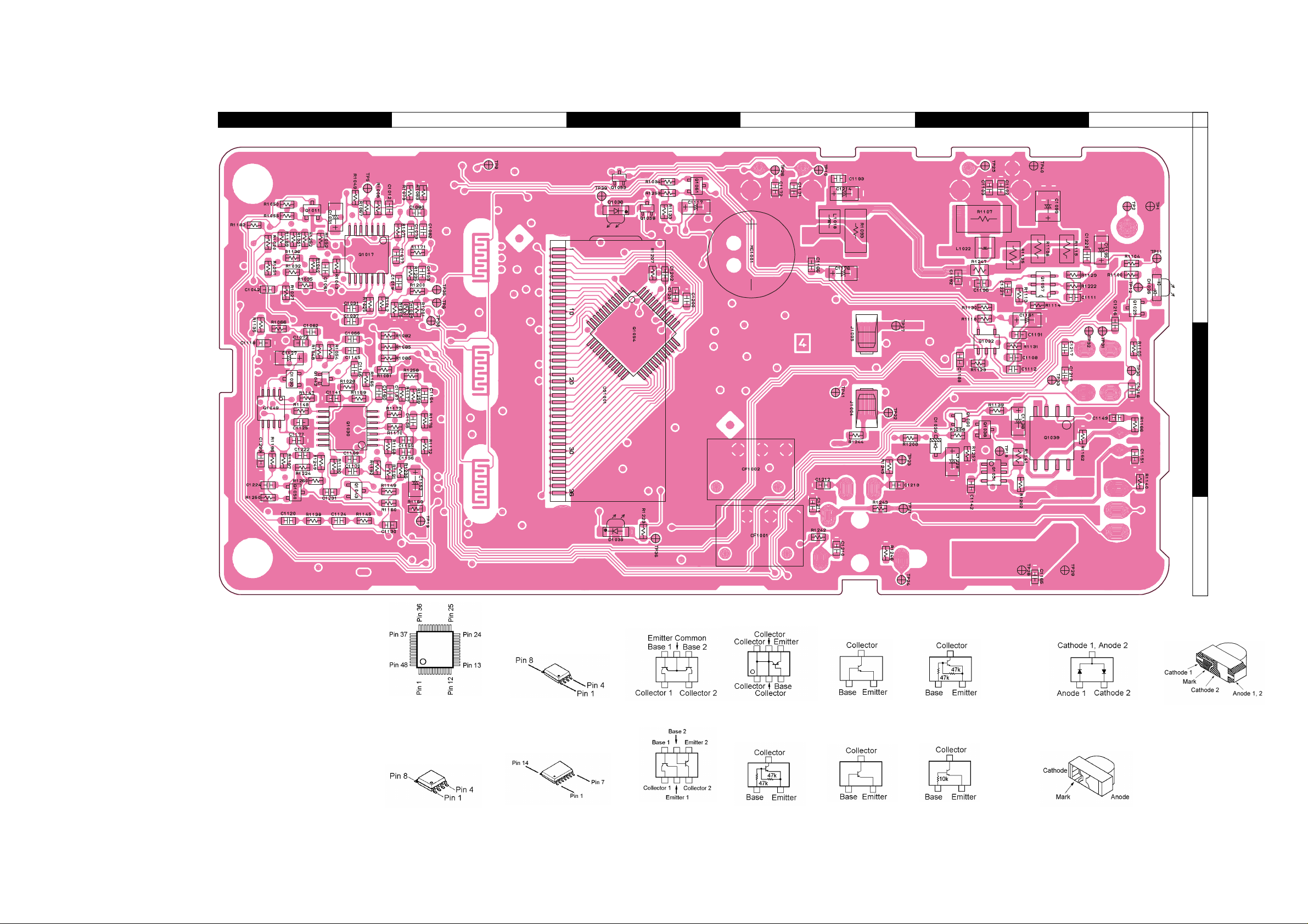
Parts Layout
MAIN Unit
C
DBA
E
F
1
2
Side A
LC75834W
(Q1054)
NJM12903R
(Q1049)
NJM2070M
(Q1039)
NJM2902V
(Q1017, 1030)
FMW1 (W1)
(Q1032)
IMZ2 (Z2)
(Q1057)
CPH6102 (AB)
(Q1051)
RT1P441U (P3)
(Q1060)
2SC4154E (LE)
(Q1025, 1038
1050, 1061)
2SA1586Y (SY)
(Q1011, 1043)
RT1N441U (N3)
(Q1042, 1053)
PDTC114TE (24)
(Q1058)
MC2850 (A7)
(D1030)
FA1101F (VX-180)
(D1035, 1038)
3
12-22SURSYGC/S530-A2/TR8
(D1026)
19
Page 19
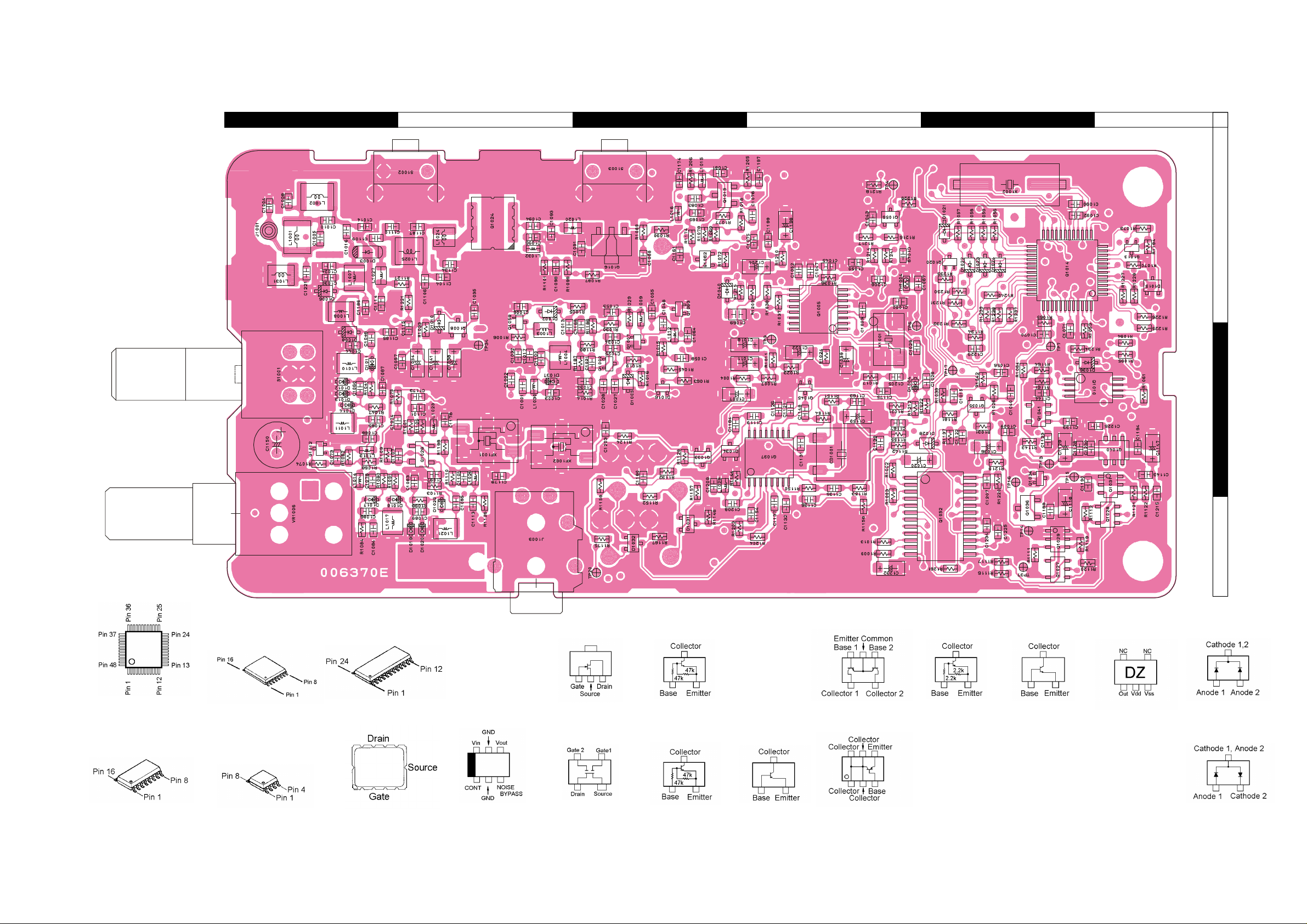
MAIN Unit
a
c
db
e
f
1
2
Side B
M37516E6HP
(Q1014)
MB15A02PFV1
(Q1005)
TA31136FN
(Q1037)
BR93LC66FV
(Q1010)
M62364FP
(Q1052)
2SK2974
(Q1024)
TK11250BMCL
(Q1040)
2SK2596 (BX)
(Q1016)
SGM2016AM (MA)
(Q1026)
RT1N441U (N3)
(Q1034, 1045
1063)
RT1P441U (P3)
(Q1013, 1020
1059)
2SA1586Y (SY)
(Q1056, 1062)
FMW1 (W1)
(Q1027, 1028)
CPH6102 (AB)
(Q1029, 1031)
DTB123EK (F12)
(Q1036)
2SC4154E (LE)
(Q1008, 1055)
2SC5005 (73)
(Q1007)
2SC5006 (24)
(Q1012)
2SC4215Y (QY)
(Q1033)
2SC5227 (LN)
(Q1015)
S-80735SN (DZ)
(Q1041)
3
DAN235E (M)
(D1014)
MC2850 (A7)
(D1015, 1033
1034, 1036)
20
Page 20

Circuit Diagram
MAIN Unit (Lot. 3~)
21
Page 21
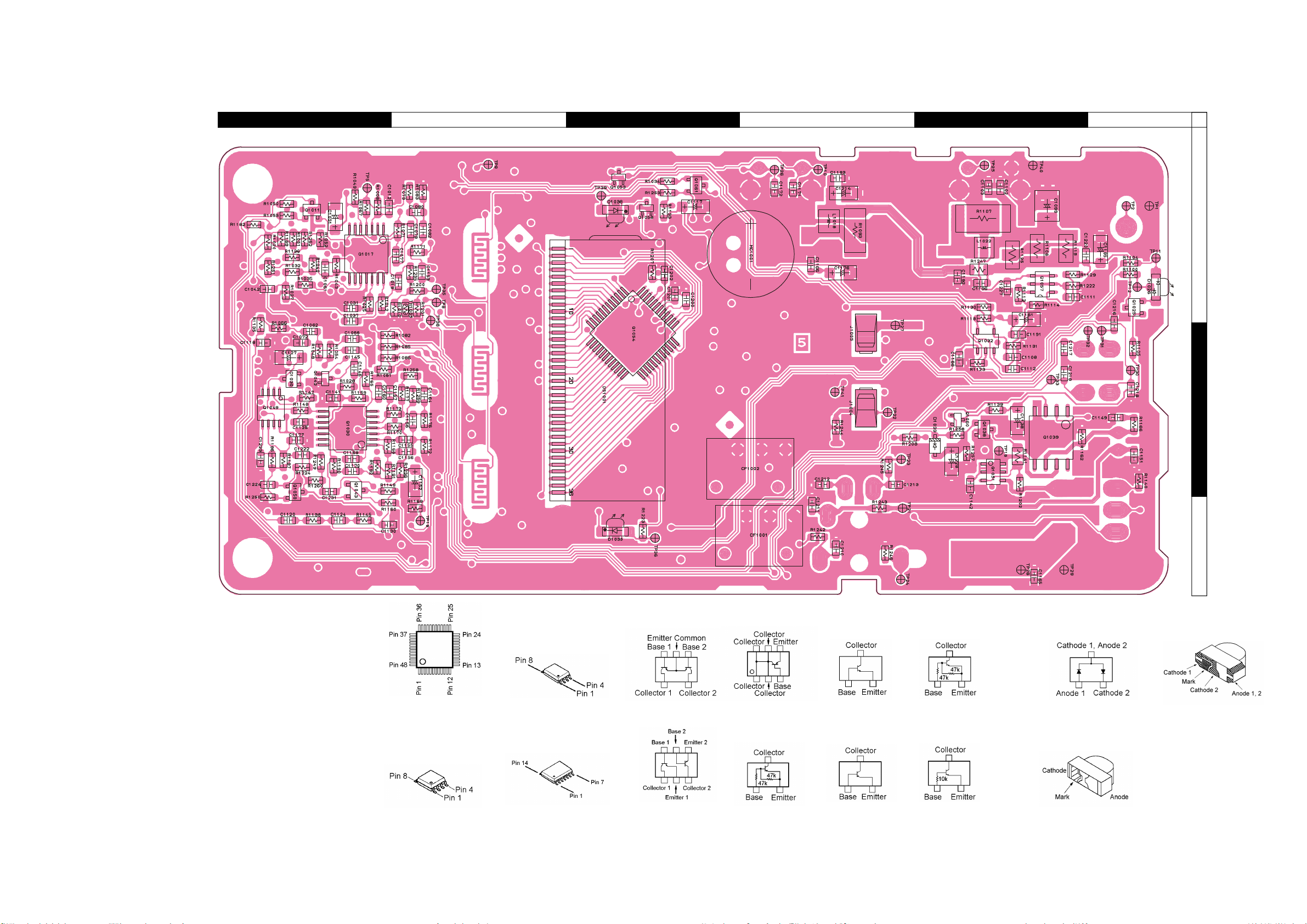
Parts Layout
MAIN Unit (Lot. 3~)
C
DBA
E
F
1
2
Side A
LC75834W
(Q1054)
NJM12903R
(Q1049)
NJM2070M
(Q1039)
NJM2902V
(Q1017, 1030)
FMW1 (W1)
(Q1032)
IMZ2 (Z2)
(Q1057)
CPH6102 (AB)
(Q1051)
RT1P441U (P3)
(Q1060)
2SC4154E (LE)
(Q1025, 1038
1050, 1061)
2SA1586Y (SY)
(Q1011, 1043)
RT1N441U (N3)
(Q1042, 1053)
PDTC114TE (24)
(Q1058)
MC2850 (A7)
(D1030)
FA1101F (VX-180)
(D1035, 1038)
3
12-22SURSYGC/S530-A2/TR8
(D1026)
VX-160V/-180V Service Manual
23
Page 22

MAIN Unit (Lot. 3~)
a
c
db
e
f
1
2
Side B
M37516E6HP
(Q1014)
MB15A02PFV1
(Q1005)
TA31136FN
(Q1037)
BR93LC66FV
(Q1010)
M62364FP
(Q1052)
2SK2974
(Q1024)
TK11250BMCL
(Q1040)
2SK2596 (BX)
(Q1016)
SGM2016AM (MA)
(Q1026)
RT1N441U (N3)
(Q1034, 1045
1063)
RT1P441U (P3)
(Q1013, 1020
1059)
2SA1586Y (SY)
(Q1056, 1062)
FMW1 (W1)
(Q1027, 1028)
CPH6102 (AB)
(Q1029, 1031)
DTB123EK (F12)
(Q1036)
2SC4154E (LE)
(Q1008, 1055)
2SC5005 (73)
(Q1007)
2SC5006 (24)
(Q1012)
2SC4215Y (QY)
(Q1033)
2SC5227 (LN)
(Q1015)
S-80735SN (DZ)
(Q1041)
3
DAN235E (M)
(D1014)
MC2850 (A7)
(D1015, 1033
1034, 1036)
24
VX-160V/-180V Service Manual
Page 23
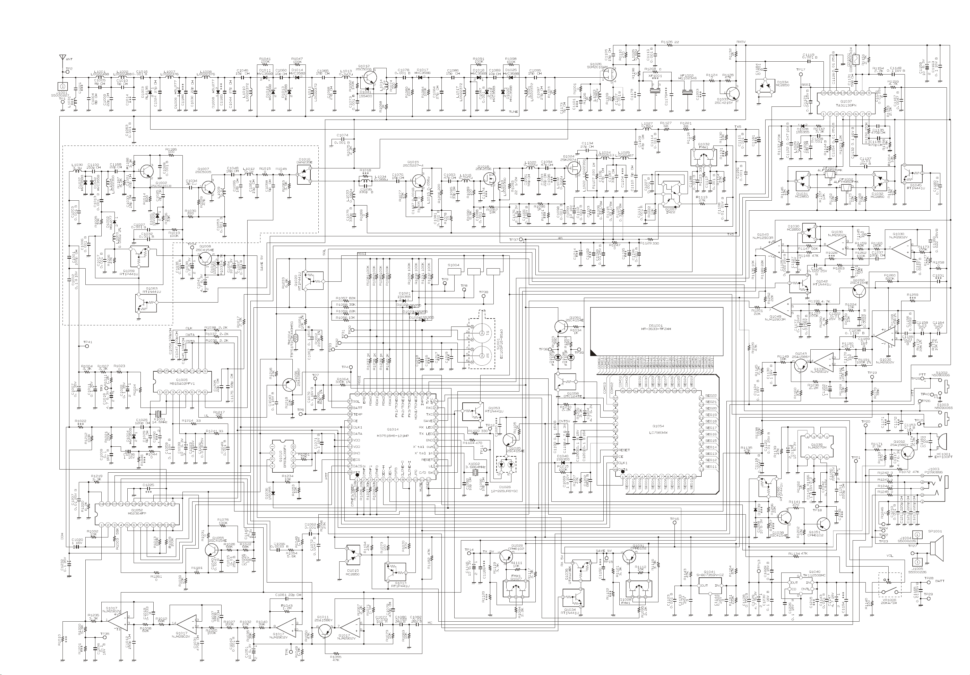
Circuit Diagram
MAIN Unit (Lot. 18~)
25
Page 24
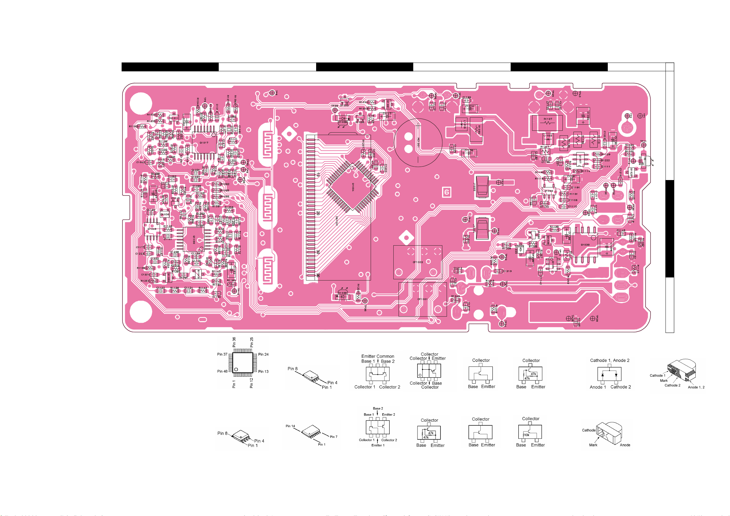
Parts Layout
MAIN Unit (Lot. 18~)
C
DBA
E
F
1
2
Side A
LC75834W
(Q1054)
NJM12903R
(Q1049)
NJM2070M
(Q1039)
NJM2902V
(Q1017, 1030)
FMW1 (W1)
(Q1032)
IMZ2 (Z2)
(Q1057)
CPH6102 (AB)
(Q1051)
RT1P441U (P3)
(Q1060)
2SC4154E (LE)
(Q1025, 1038
1050, 1061)
2SA1586Y (SY)
(Q1011, 1043)
RT1N441U (N3)
(Q1042, 1053)
PDTC114TE (24)
(Q1058)
MC2850 (A7)
(D1030)
FA1101F (VX-180)
(D1035, 1038)
3
12-22SURSYGC/S530-A2/TR8
(D1026)
VX-160V/-180V Service Manual
27
Page 25

MAIN Unit (Lot. 18~)
a
c
db
e
f
1
2
Side B
M37516E6HP
(Q1014)
MB15A02PFV1
(Q1005)
TA31136FN
(Q1037)
BR93LC66FV
(Q1010)
M62364FP
(Q1052)
2SK2974
(Q1024)
TK11250BMCL
(Q1040)
2SK2596 (BX)
(Q1016)
SGM2016AM (MA)
(Q1026)
RT1N441U (N3)
(Q1034, 1045
1063)
RT1P441U (P3)
(Q1013, 1020
1059)
2SA1586Y (SY)
(Q1056, 1062)
FMW1 (W1)
(Q1027, 1028)
CPH6102 (AB)
(Q1029, 1031)
DTB123EK (F12)
(Q1036)
2SC4154E (LE)
(Q1008, 1055)
2SC5005 (73)
(Q1007)
2SC5006 (24)
(Q1012)
2SC4215Y (QY)
(Q1033)
2SC5227 (LN)
(Q1015)
S-80735SN (DZ)
(Q1041)
3
DAN235E (M)
(D1014)
MC2850 (A7)
(D1015, 1033
1034, 1036)
28
VX-160V/-180V Service Manual
Page 26

MAIN Unit
Parts List
DESCRIPTION VALUE V/W TOL. VXSTD P/NMFR’S DESIG VERS.REF. LOT. SIDE LAY ADR
*** MAIN UNIT ***
PCB with Components CB1390001 VX-160
PCB with Components CB1390002 VX-180
Printed Circuit Board FR006370E 1Printed Circuit Board FR006370G 3-
C 1001 CHIP CAP. 100pF 50V CH GRM39CH101J50PT K22174235 1- B b2
C 1002 CHIP CAP. 0.1uF 16V B GRM39B104K16PT K22124805 1- B b2
C 1003 CHIP CAP. 0.001uF 50V B GRM39B102K50PT K22174821 1- B b2
C 1004 CHIP CAP. 8pF 50V CH GRM39CH080D50PT K22174209 1- B a1
C 1005 CHIP CAP. 8pF 50V CH GRM39CH080D50PT K22174209 1- B a1
C 1006 CHIP CAP. 0.001uF 50V B GRM39B102K50PT K22174821 1- B b1
C 1007 CHIP TA.CAP. 0.1uF 35V TESVA1V104M1-8R K78160025 1- B c2
C 1008 CHIP CAP. 22pF 50V CH GRM39CH220J50PT K22174219 1- B a1
C 1009 CHIP CAP. 0.1uF 16V B GRM39B104K16PT K22124805 1- B e2
C 1010 CHIP CAP. 5pF 50V CH GRM39CH050C50PT K22174206 1- B a1
C 1011 CHIP TA.CAP. 0.1uF 35V TESVA1V104M1-8R K78160025 1- B c2
C 1012 CHIP CAP. 150pF 50V CH GRM39CH151J50PT K22174239 1- A A1
C 1013 CHIP CAP. 0.001uF 50V B GRM39B102K50PT K22174821 1- B b2
C 1015 CHIP CAP. 0.01uF 25V B GRM39B103K25PT K22144803 1- B e2
C 1016 CHIP CAP. 0.001uF 50V B GRM39B102K50PT K22174821 1- B a1
C 1017 CHIP CAP. 0.001uF 50V B GRM39B102K50PT K22174821 1- B b2
C 1018 CHIP TA.CAP. 4.7uF 6.3V TEMSVA0J475M-8R K78080017 1- B c2
C 1019 CHIP CAP. 0.0033uF 50V B GRM39B332K50PT K22174831 1- A B1
C 1020 CHIP TA.CAP. 1uF 16V TESVA1C105M1-8R K78120009 1- B d2
C 1021 CHIP CAP. 22pF 50V CH GRM36CH220J50PT K22178220 1- B c2
C 1022 CHIP TA.CAP. 0.1uF 35V TESVA1V104M1-8R K78160025 1- B d2
C 1023 CHIP CAP. 0.1uF 16V B GRM39B104K16PT K22124805 1- B d1
C 1024 CHIP CAP. 27pF 50V CH GRM39CH270J50PT K22174221 1- B a1
C 1025 CHIP CAP. 2pF 50V CK GRM39CK020C50PT K22174203 1- B c2
C 1026 CHIP CAP. 120pF 50V CH GRM39CH121J50PT K22174237 1- B e2
C 1027 CHIP CAP. 0.001uF 50V B GRM39B102K50PT K22174821 1- B c2
C 1028 CHIP CAP. 0.001uF 50V B GRM39B102K50PT K22174821 1- B c2
C 1029 CHIP CAP. 6pF 50V CH GRM39CH060D50PT K22174207 1- B d2
C 1030 CHIP CAP. 22pF 50V CH GRM39CH220J50PT K22174219 1- B a1
C 1031 CHIP CAP. 470pF 50V CH GRM39CH471J50PT K22174249 1- A A1
C 1032 CHIP CAP. 0.001uF 50V B GRM39B102K50PT K22174821 1- B b2
C 1033 CHIP CAP. 18pF 50V CH GRM39CH180J50PT K22174217 1- B c2
C 1034 CHIP CAP. 3pF 50V CJ GRM39CJ030C50PT K22174204 1- B c2
C 1035 CHIP CAP. 0.001uF 50V B GRM39B102K50PT K22174821 1- B b1
C 1036 CHIP TA.CAP. 1uF 16V TESVA1C105M1-8R K78120009 1- B e2
C 1037 CHIP CAP. 680pF 25V CH GRM39CH681J25PT K22144203 1- A A2
C 1038 CHIP TA.CAP. 2.2uF 6.3V TESVA0J225M1-8R K78080009 1- B b2
C 1039 CHIP TA.CAP. 10uF 6.3V TEMSVA0J106M-8R K78080027 1- B d2
C 1040 CHIP CAP. 0.0047uF 50V B GRM39B472K50PT K22174833 1- B e2
C 1041 CHIP TA.CAP. 4.7uF 6.3V TEMSVA0J475M-8R K78080017 1- B b2
C 1042 CHIP CAP. 0.001uF 50V B GRM39B102K50PT K22174821 1- A A1
C 1043 CHIP CAP. 0.1uF 16V B GRM39B104K16PT K22124805 1- B d1
C 1044 CHIP CAP. 27pF 50V CH GRM39CH270J50PT K22174221 1- B a2
C 1045 CHIP CAP. 100pF 50V CH GRM39CH101J50PT K22174235 1- B d1
C 1046 CHIP CAP. 15pF 50V CH GRM39CH150J50PT K22174215 1- B a2
C 1047 CHIP CAP. 100pF 50V CH GRM39CH101J50PT K22174235 1- B d1
C 1048 CHIP CAP. 18pF 50V CH GRM39CH180J50PT K22174217 1- B c1
C 1049 CHIP CAP. 0.001uF 50V B GRM39B102K50PT K22174821 1- B d1
C 1051 CHIP TA.CAP. 10uF 6.3V TEMSVA0J106M-8R K78080027 1- A A1
C 1052 CHIP CAP. 100pF 50V CH GRM39CH101J50PT K22174235 1- B d1
C 1053 CHIP CAP. 0.001uF 50V B GRM39B102K50PT K22174821 1- B c1
C 1054 CHIP TA.CAP. 10uF 6.3V TEMSVA0J106M-8R K78080027 1- B b2
C 1055 CHIP CAP. 12pF 50V CH GRM39CH120J50PT K22174213 1- B c1
C 1056 CHIP CAP. 0.047uF 16V B GRM39B473K16PT K22124804 1- B e2
C 1057 CHIP CAP. 0.001uF 50V B GRM39B102K50PT K22174821 1- B b2
C 1058 CHIP CAP. 5pF 50V CH GRM39CH050C50PT K22174206 1- B c2
C 1059 CHIP CAP. 0.1uF 16V B GRM39B104K16PT K22124805 1- B d1
C 1060 CHIP CAP. 10pF 50V CH GRM39CH100D50PT K22174211 1- B a2
C 1061 CHIP CAP. 22pF 50V CH GRM39CH220J50PT K22174219 1- A A1
C 1062 CHIP CAP. 0.001uF 50V B GRM39B102K50PT K22174821 1- A A1
C 1063 CHIP CAP. 0.001uF 50V B GRM39B102K50PT K22174821 1- B b2
C 1064 CHIP CAP. 15pF 50V CH GRM39CH150J50PT K22174215 1- B c2
Printed Circuit Board FR006370H 18-
29
Page 27

MAIN Unit
DESCRIPTION VALUE V/W TOL. VXSTD P/NMFR’S DESIG VERS.REF. LOT. SIDE LAY ADR
C 1065 CHIP CAP. 15pF 50V CH GRM39CH150J50PT K22174215 1- B a2
C 1066 CHIP CAP. 0.0033uF 50V B GRM39B332K50PT K22174831 1- A A2
C 1067 CHIP CAP. 0.1uF 16V B GRM39B104K16PT K22124805 1- B d1
C 1068 CHIP CAP. 27pF 50V CH GRM39CH270J50PT K22174221 1- B a2
C 1070 CHIP CAP. 0.1uF 16V B GRM39B104K16PT K22124805 1- B e2
C 1071 CHIP CAP. 0.1uF 16V B GRM39B104K16PT K22124805 1- B e2
C 1072 CHIP CAP. 0.0047uF 50V B GRM39B472K50PT K22174833 1- A A2
C 1073 CHIP CAP. 0.001uF 50V B GRM39B102K50PT K22174821 1- B a2
C 1074 CHIP CAP. 0.001uF 50V B GRM39B102K50PT K22174821 1- B a2
C 1075 CHIP CAP. 330pF 50V B GRM39B331K50PT K22174820 1- B d1
C 1076 CHIP CAP. 15pF 50V CH GRM39CH150J50PT K22174215 1- B d1
C 1077 CHIP CAP. 0.033uF 16V R GRM39R333K16PT K22124801 1- A B1
C 1078 CHIP CAP. 0.001uF 50V B GRM39B102K50PT K22174821 1- B a2
C 1079 CHIP CAP. 470pF 50V CH GRM39CH471J50PT K22174249 1- A B1
C 1080 CHIP CAP. 0.022uF 25V B GRM39B223K25PT K22144807 1- A B1
C 1081 CHIP CAP. 0.001uF 50V B GRM39B102K50PT K22174821 1- B c1
C 1082 CHIP CAP. 0.01uF 25V B GRM39B103K25PT K22144803 1- A B1
C 1083 CHIP CAP. 47pF 50V CH GRM39CH470J50PT K22174227 1- B c1
C 1084 CHIP CAP. 27pF 50V CH GRM39CH270J50PT K22174221 1- B a3
C 1085 CHIP CAP. 33pF 50V CH GRM39CH330J50PT K22174223 1- B c1
C 1086 CHIP CAP. 15pF 50V CH GRM39CH150J50PT K22174215 1- B a3
C 1087 CHIP CAP. 0.001uF 50V B GRM39B102K50PT K22174821 1- B a2
C 1088 CHIP CAP. 0.001uF 50V B GRM39B102K50PT K22174821 1- B c1
C 1089 CHIP CAP. 10pF 50V CH GRM39CH100D50PT K22174211 1- B b3
C 1090 CHIP CAP. 10pF 50V CH GRM39CH100D50PT K22174211 1- B e1
C 1091 CHIP CAP. 56pF 50V CH GRM39CH560J50PT K22174229 1- B c1
C 1092 CHIP CAP. 10pF 50V CH GRM39CH100D50PT K22174211 1- B e1
C 1093 CHIP CAP. 22pF 50V CH GRM39CH220J50PT K22174219 1- B b1
C 1094 CHIP CAP. 47pF 50V CH GRM39CH470J50PT K22174227 1- B b1
C 1095 CHIP CAP. 15pF 50V CH GRM39CH150J50PT K22174215 1- B b3
C 1097 CHIP CAP. 27pF 50V CH GRM39CH270J50PT K22174221 1- B b2
C 1098 CHIP CAP. 0.001uF 50V B GRM39B102K50PT K22174821 1- B b1
C 1099 CHIP TA.CAP. 10uF 16V TEMSVB21C106M-8R K78120025 1- A E1
C 1100 CHIP CAP. 150pF 50V CH GRM39CH151J50PT K22174239 1- B b2
C 1102 CHIP CAP. 0.001uF 50V B GRM39B102K50PT K22174821 1- A E1
C 1105 CHIP CAP. 15pF 50V CH GRM39CH150J50PT K22174215 1- B b2
C 1106 CHIP CAP. 47pF 50V CH GRM39CH470J50PT K22174227 1- B b1
C 1107 CHIP CAP. 0.001uF 50V B GRM39B102K50PT K22174821 1- B a2
C 1108 CHIP CAP. 0.01uF 25V B GRM39B103K25PT K22144803 1- A E2
C 1109 CHIP CAP. 47pF 50V CH GRM39CH470J50PT K22174227 1- B a1
C 1110 CHIP CAP. 5pF 50V CH GRM39CH050C50PT K22174206 1- B a1
C 1111 CHIP CAP. 0.001uF 50V B GRM39B102K50PT K22174821 1- A E1
C 1112 CHIP CAP. 0.001uF 50V B GRM39B102K50PT K22174821 1- A E2
C 1113 CHIP CAP. 0.001uF 50V B GRM39B102K50PT K22174821 1- B b3
C 1114 CHIP CAP. 0.001uF 50V B GRM39B102K50PT K22174821 1- B a1
C 1115 CHIP CAP. 0.001uF 50V B GRM39B102K50PT K22174821 1- B b2
C 1116 CHIP TA.CAP. 10uF 6.3V TEMSVA0J106M-8R K78080027 1- B e3
C 1117 CHIP TA.CAP. 4.7uF 6.3V TEMSVA0J475M-8R K78080017 1- A C1
C 1118 CHIP CAP. 0.0047uF 50V B GRM39B472K50PT K22174833 1- A A2
C 1119 CHIP CAP. 0.001uF 50V B GRM39B102K50PT K22174821 1- B d2
C 1120 CHIP CAP. 0.01uF 25V B GRM39B103K25PT K22144803 1- A A3
C 1121 CHIP CAP. 0.047uF 16V B GRM39B473K16PT K22124804 1- B d2
C 1122 CHIP CAP. 0.047uF 16V B GRM39B473K16PT K22124804 1- B e2
C 1123 CHIP CAP. 0.001uF 50V B GRM39B102K50PT K22174821 1- B e2
C 1124 CHIP CAP. 0.1uF 16V B GRM39B104K16PT K22124805 1- A A3
C 1125 CHIP CAP. 0.01uF 25V B GRM39B103K25PT K22144803 1- A A2
C 1125 CHIP CAP. 0.022uF 25V B GRM39B223K25PT K22144807 18- A A2
C 1126 CHIP CAP. 0.01uF 25V B GRM39B103K25PT K22144803 1- B d2
C 1127 CHIP TA.CAP. 1uF 16V TESVA1C105M1-8R K78120009 1- A A2
C 1128 CHIP CAP. 0.001uF 50V B GRM39B102K50PT K22174821 1- B e2
C 1129 CHIP TA.CAP. 4.7uF 6.3V TEMSVA0J475M-8R K78080017 1- B e2
C 1130 CHIP CAP. 0.1uF 16V B GRM39B104K16PT K22124805 1- A A3
C 1131 CHIP CAP. 56pF 50V CH GRM39CH560J50PT K22174229 1- B d2
C 1132 CHIP CAP. 0.1uF 16V B GRM39B104K16PT K22124805 1- B d3
C 1133 CHIP CAP. 0.01uF 25V B GRM39B103K25PT K22144803 1- B e2
C 1134 CHIP CAP. 27pF 50V CH GRM39CH270J50PT K22174221 1- B b1
C 1135 CHIP CAP. 470pF 50V CH GRM39CH471J50PT K22174249 1- B d2
C 1136 CHIP CAP. 470pF 50V CH GRM39CH471J50PT K22174249 1- B d3
30
Page 28
MAIN Unit
DESCRIPTION VALUE V/W TOL. VXSTD P/NMFR’S DESIG VERS.REF. LOT. SIDE LAY ADR
C 1137 CHIP CAP. 0.01uF 25V B GRM39B103K25PT K22144803 1- B d3
C 1138 CHIP TA.CAP. 10uF 6.3V TEMSVA0J106M-8R K78080027 1- A E2
C 1139 CHIP CAP. 0.01uF 25V B GRM39B103K25PT K22144803 1- B d2
C 1140 CHIP CAP. 2.2uF 10V B GRM42-6B225K10PT K22101801 18- B e1
C 1141 CHIP CAP. 0.001uF 50V B GRM39B102K50PT K22174821 1- A A2
C 1141 CHIP CAP. 100pF 50V CH GRM39CH101J50PT K22174235 18- A A2
C 1142 CHIP CAP. 0.1uF 16V B GRM39B104K16PT K22124805 1- A E2
C 1143 CHIP CAP. 0.001uF 50V B GRM39B102K50PT K22174821 1- B f2
C 1144 CHIP CAP. 0.022uF 25V B GRM39B223K25PT K22144807 1- B e2
C 1144 CHIP CAP. 0.1uF 16V B GRM39B104K16PT K22124805 18- B e2
C 1145 CHIP CAP. 0.022uF 25V B GRM39B223K25PT K22144807 1- A A2
C 1145 CHIP CAP. 0.1uF 16V B GRM39B104K16PT K22124805 18- A A2
C 1146 CHIP CAP. 0.0033uF 50V B GRM39B332K50PT K22174831 1- A A2
C 1147 CHIP TA.CAP. 4.7uF 16V TEMSVA1C475M-8R K78120031 1- B f2
C 1148 CHIP CAP. 0.1uF 16V B GRM39B104K16PT K22124805 1- B d2
C 1149 CHIP CAP. 0.1uF 16V B GRM39B104K16PT K22124805 1- A F2
C 1150 AL.ELECTRO.CAP. 220uF 10V SMG1AVB221M 220UF K40109027 1- B a2
C 1151 CHIP CAP. 220pF 50V CH GRM39CH221J50PT K22174243 1- A F2
C 1152 CHIP TA.CAP. 1uF 16V TESVA1C105M1-8R K78120009 1- A B2
C 1153 CHIP CAP. 0.1uF 16V B GRM39B104K16PT K22124805 1- A B1
C 1154 CHIP CAP. 0.01uF 25V B GRM39B103K25PT K22144803 1- B d3
C 1155 CHIP CAP. 0.01uF 25V B GRM39B103K25PT K22144803 1- A B2
C 1156 CHIP CAP. 0.0022uF 50V B GRM39B222K50PT K22174822 1- A B2
C 1157 CHIP CAP. 0.0047uF 50V B GRM39B472K50PT K22174833 1- A A2
C 1157 CHIP CAP. 0.0033uF 50V B GRM39B332K50PT K22174831 18- A A2
C 1158 CHIP CAP. 0.01uF 25V B GRM39B103K25PT K22144803 1- A B2
C 1159 CHIP TA.CAP. 10uF 6.3V TEMSVA0J106M-8R K78080027 1- B d2
C 1160 CHIP CAP. 0.01uF 25V B GRM39B103K25PT K22144803 1- A A2
C 1160 CHIP CAP. 0.022uF 25V B GRM39B223K25PT K22144807 18- A A2
C 1161 CHIP CAP. 0.001uF 50V B GRM39B102K50PT K22174821 1- B c1
C 1163 CHIP CAP. 0.1uF 16V B GRM39B104K16PT K22124805 1- B d2
C 1164 CHIP CAP. 0.01uF 25V B GRM39B103K25PT K22144803 1- A B2
C 1165 CHIP CAP. 0.01uF 25V B GRM39B103K25PT K22144803 1- A E3
C 1166 CHIP CAP. 0.1uF 16V B GRM39B104K16PT K22124805 1- A D1
C 1167 CHIP CAP. 0.0047uF 50V B GRM39B472K50PT K22174833 1- B d2
C 1168 CHIP CAP. 22pF 50V CH GRM39CH220J50PT K22174219 1- B c2
C 1169 CHIP CAP. 0.1uF 16V B GRM39B104K16PT K22124805 1- A A2
C 1170 CHIP CAP. 0.1uF 16V B GRM39B104K16PT K22124805 1- A A2
C 1173 CHIP CAP. 7pF 50V CH GRM39CH070D50PT K22174208 1- B b2
C 1175 CHIP CAP. 68pF 50V CH GRM39CH680J50PT K22174231 1- B d2
C 1176 CHIP TA.CAP. 2.2uF 6.3V TESVA0J225M1-8R K78080009 1- A D1
C 1177 CHIP CAP. 0.1uF 16V B GRM39B104K16PT K22124805 1- A A2
C 1180 CHIP CAP. 0.1uF 16V B GRM39B104K16PT K22124805 1- B c2
C 1184 CHIP CAP. 0.001uF 50V B GRM39B102K50PT K22174821 1- B c2
C 1187 CHIP CAP. 33pF 50V CH GRM39CH330J50PT K22174223 1- B b1
C 1188 CHIP CAP. 0.001uF 50V B GRM39B102K50PT K22174821 1- A E2
C 1191 CHIP CAP. 0.001uF 50V B GRM39B102K50PT K22174821 1- A E2
C 1193 CHIP CAP. 0.01uF 25V B GRM39B103K25PT K22144803 1- A D1
C 1196 CHIP CAP. 0.001uF 50V B GRM39B102K50PT K22174821 1- A E1
C 1197 CHIP CAP. 0.001uF 50V B GRM39B102K50PT K22174821 1- B d1
C 1198 CHIP TA.CAP. 4.7uF 6.3V TEMSVA0J475M-8R K78080017 VX-180 1- B d1
C 1199 CHIP CAP. 0.1uF 16V B GRM39B104K16PT K22124805 VX-180 1- B d1
C 1200 CHIP CAP. 0.1uF 16V B GRM39B104K16PT K22124805 VX-180 1- A C1
C 1201 CHIP CAP. 0.1uF 16V B GRM39B104K16PT K22124805 VX-180 1- A C1
C 1202 CHIP CAP. 680pF 50V B GRM39B681M50PT K22174807 VX-180 1- A C1
C 1204 CHIP TA.CAP. 4.7uF 6.3V TEMSVA0J475M-8R K78080017 VX-180 1- B d1
C 1205 CHIP CAP. 22pF 50V CH GRM39CH220J50PT K22174219 1- B d2
C 1206 CHIP CAP. 0.01uF 25V B GRM39B103K25PT K22144803 1- B d1
C 1207 CHIP CAP. 0.01uF 25V B GRM39B103K25PT K22144803 1- B e2
C 1208 CHIP CAP. 0.001uF 50V B GRM39B102K50PT K22174821 1- B c3
C 1209 CHIP CAP. 12pF 50V CH GRM39CH120J50PT K22174213 1- B c2
C 1210 CHIP CAP. 0.001uF 50V B GRM39B102K50PT K22174821 1- A D3
C 1211 CHIP CAP. 220pF 50V CH GRM39CH221J50PT K22174243 1- A D3
C 1212 CHIP CAP. 220pF 50V CH GRM39CH221J50PT K22174243 1- A D2
C 1213 CHIP CAP. 220pF 50V CH GRM39CH221J50PT K22174243 1- A D2
C 1222 CHIP CAP. 0.01uF 25V B GRM39B103K25PT K22144803 1- A A2
C 1223 CHIP CAP. 0.01uF 25V B GRM39B103K25PT K22144803 1- A A2
C 1224 CHIP CAP. 0.0022uF 50V B GRM39B222K50PT K22174822 1- A A2
31
Page 29

MAIN Unit
DESCRIPTION VALUE V/W TOL. VXSTD P/NMFR’S DESIG VERS.REF. LOT. SIDE LAY ADR
C 1226 CHIP CAP. 0.1uF 16V B GRM39B104K16PT K22124805 1- B e2
C 1227 CHIP CAP. 0.001uF 50V B GRM39B102K50PT K22174821 1- A E1
C 1228 CHIP TA.CAP. 10uF 6.3V TEMSVA0J106M-8R K78080027 1- A E2
C 1229 CHIP CAP. 0.1uF 16V B GRM39B104K16PT K22124805 1- B e2
C 1230 CHIP CAP. 0.1uF 16V B GRM39B104K16PT K22124805 1- B e2
C 1231 CHIP CAP. 0.1uF 16V B GRM39B104K16PT K22124805 1- A A2
C 1232 CHIP TA.CAP. 0.1uF 35V TESVA1V104M1-8R K78160025 1- B d3
C 1235 CHIP CAP. 330pF 50V CH GRM39CH331J50PT K22174253 1- B c1
C 1235 CHIP CAP. 330pF 50V B GRM39B331K50PT K22174820 3- B c1
C 1236 CHIP CAP. 0.1uF 16V B GRM39B104K16PT K22124805 1- A B1
C 1237 CHIP CAP. 180pF 50V CH GRM39CH181J50PT K22174241 18- A A2
C 1238 CHIP CAP. 0.1uF 16V B GRM39B104K16PT K22124805 18- A A2
CD1001 CERAMIC DISC CDBC450CX24-TC H7901340 1- B d2
CF1001 CERAMIC FILTER ALFYM450G=K H3900534 1- A C3
CF1002 CERAMIC FILTER ALFYM450F=K H3900531 1- A C2
D 1002 DIODE HSU277TRF G2070118 1- B b1
D 1003 DIODE RLS135 TE-11 G2070128 1- B a1
D 1004 DIODE HVC350B-TRF G2070596 1- B d2
D 1005 DIODE 1SV229 TPH3 G2070256 1- B c2
D 1006 DIODE HSU277TRF G2070118 1- B a1
D 1008 DIODE HSU277TRF G2070118 1- B a2
D 1010 DIODE 1SS355 TE-17 G2070470 1- B b1
D 1011 DIODE HVC358B(TAPE) G2070590 1- B a2
D 1012 DIODE HVC358B(TAPE) G2070590 1- B a2
D 1013 DIODE HVC358B(TAPE) G2070590 1- B a2
D 1014 DIODE HVC358B(TAPE) G2070590 1- B a2
D 1015 DIODE MC2850-T11-1 G2070704 1- B f1
D 1016 DIODE DAN235E TL G2070612 1- B c2
D 1017 DIODE HVC358B(TAPE) G2070590 1- B a3
D 1018 DIODE HVC358B(TAPE) G2070590 1- B a3
D 1019 DIODE HVC358B(TAPE) G2070590 1- B b3
D 1020 DIODE HVC358B(TAPE) G2070590 1- B b3
D 1021 DIODE 1SS355 TE-17 G2070470 1- B e1
D 1022 DIODE 1SS355 TE-17 G2070470 1- B e1
D 1023 DIODE 1SS355 TE-17 G2070470 1- B e1
D 1024 DIODE 1SS355 TE-17 G2070470 1- B e1
D 1025 DIODE HVC358B(TAPE) G2070590 1- B b3
D 1026 LED
D 1028 DIODE 1SS355 TE-17 G2070470 1- B e2
D 1030 DIODE MC2850-T11-1 G2070704 1- A A2
D 1031 DIODE MC2850-T11-1 G2070704 1- B c3
D 1032 DIODE MC2850-T11-1 G2070704 1- B c3
D 1034 DIODE MC2850-T11-1 G2070704 1- B c2
D 1035 LED FA1101F-TR G2070842 VX-180 1- A C3
D 1036 DIODE 1SS355 TE-17 G2070470 1- B e2
D 1037 DIODE HVC358B(TAPE) G2070590 1- B b2
D 1038 LED FA1101F-TR G2070842 VX-180 1- A C1
D 1040 DIODE 1SS355 TE-17 G2070470 VX-180 1- B c1
D 1041 DIODE 1SS355 TE-17 G2070470 1- B a2
D 1041 DIODE 1SS400 TE61 G2070634 3- B a2
D 1042 DIODE HVU355TRF G2070410 1- B b2
D 1042 DIODE HVC355B(TAPE) G2070588 3- B b2
DS1001 LCD HT-3633-TFZWH G6090139 VX-180 1- A C2
J 1001 SPRING CONECTOR MS0062-10 S5000227 1- B a1
J 1003 CONNECTOR HSJ1594-010055 P1090896 1- B b3
J 1004 SHIELD FINGER 3525 3100103 S5000226 1- A D2
J 1005 SHIELD FINGER 3525 3100103 S5000226 1- A D2
L 1001 COIL E2 0.5-2.0-6T-R L0022488 1- B a1
L 1002 COIL E2 0.5-2.0-6T-R L0022488 1- B a1
L 1003 M.RFC 0.056uH C2012C-56NK L1690673 1- B b2
L 1003 M.RFC 0.056uH 2% C2012C-56NG L1690773 3- B b2
L 1004 COIL E2 0.35-1.6-7T-L L0022390 1- B b2
L 1007 COIL E2 0.3-1.7-8T-L L0022376 1- B a1
L 1008 COIL E2 0.3-1.7-8T-L L0022376 1- B a1
L 1009 M.RFC 0.1uH HK1608 R10J-T L1690528 1- B c1
L 1010 COIL E2 0.3-1.7-7T-R L0022372 1- B a2
L 1011 COIL E2 0.3-1.7-7T-R L0022372 1- B a2
L 1012 M.RFC 0.1uH HK1608 R10J-T L1690528 1- B c2
12-22SURSYGC/S530-A2/TR8
G2070810 1- A F1
32
Page 30

MAIN Unit
DESCRIPTION VALUE V/W TOL. VXSTD P/NMFR’S DESIG VERS.REF. LOT. SIDE LAY ADR
L 1013 M.RFC 0.047uH HK1608 47NJ-T L1690524 1- B a2
L 1014 M.RFC 0.1uH HK1608 R10J-T L1690528 1- B a2
L 1015 M.RFC 0.056uH HK1608 56NJ-T L1690525 1- B c1
L 1016 M.RFC 0.047uH HK1608 47NJ-T L1690524 1- B c1
L 1017 COIL E2 0.3-1.7-7T-R L0022372 1- B a3
L 1018 COIL E2 0.35-1.6-7T-L L0022390 1- A D1
L 1020 M.RFC 0.022uH HK2125 22NK-T L1690381 1- B b1
L 1021 COIL E2 0.3-1.7-7T-R L0022372 1- B b3
L 1022 COIL E2 0.45-1.4-4T-L L0022391 1- A E1
L 1023 M.RFC 0.082uH HK1608 82NJ-T L1690527 1- B b2
L 1024 COIL E2 0.5-1.4-2.5T-L L0022613 1- B b1
L 1025 COIL E2 0.5-2.0-5T-R L0022487 1- B b1
L 1026 M.RFC 0.82uH LK1608 R82K-T L1690417 1- B b2
L 1027 M.RFC 0.82uH LK2125 R82K-T L1690318 1- B a1
L 1029 M.RFC 0.82uH LK1608 R82K-T L1690417 1- B c2
L 1030 M.RFC 3.3uH LK1608 3R3K-T L1690686 1- B b2
L 1032 M.RFC 0.022uH HK1608 22NJ-T L1690520 1- B b1
L 1033 M.RFC 0.082uH HK1608 82NJ-T L1690527 1- B c1
L 1034 M.RFC 0.068uH LK1608 68NM-T L1690406 1- B c1
MC1001 MIC. ELEMENT EM-100PT M3290029 1- A D1
Q 1002 TRANSISTOR 2SC5231C8-TL G3352318H 1- B c2
Q 1005 IC MB15A02PFV1-G-BND-EF G1092541 1- B d1
Q 1007 TRANSISTOR 2SC5005-T1 G3350058 1- B c2
Q 1008 TRANSISTOR 2SC4154-T11-1E G3341548E 1- B b2
Q 1010 IC BR93LC66FV-E2 G1092853 1- B e2
Q 1011 TRANSISTOR 2SA1586Y TE85R G3115867Y 1- A A1
Q 1012 TRANSISTOR 2SC5006-T1 G3350068 1- B a2
Q 1013 TRANSISTOR RT1P441U-T11-1 G3070248 1- B f1
Q 1014 IC M37516M6-121HP G1093530 1- B e1
Q 1015 TRANSISTOR 2SC5227-4-TB G3352278D 1- B c1
Q 1016 FET 2SK2596BXTL G3825967 1- B c1
Q 1017 IC NJM2902V-TE1 G1091679 1- A A1
Q 1020 TRANSISTOR RT1P441U-T11-1 G3070248 1- B e1
Q 1024 FET 2SK2974-T11 G3829747 1- B b1
Q 1025 TRANSISTOR 2SC4154-T11-1E G3341548E 1- A F1
Q 1026 FET SGM2016AM-T7 G4070012 1- B b2
Q 1027 TRANSISTOR FMW1 T98 G3070009 1- B e3
Q 1028 TRANSISTOR FMW1 T98 G3070009 1- B f3
Q 1029 TRANSISTOR CPH6102-TL G3070223 1- B e3
Q 1030 IC NJM2902V-TE1 G1091679 1- A A2
Q 1031 TRANSISTOR CPH6102-TL G3070223 1- B f2
Q 1032 TRANSISTOR FMW1 T98 G3070009 1- A E2
Q 1033 TRANSISTOR 2SC4215Y TE85R G3342157Y 1- B c2
Q 1034 TRANSISTOR RT1N441U-T11-1 G3070247 1- B e2
Q 1036 TRANSISTOR DTB123EK T146 G3070022 1- B e3
Q 1037 IC TA31136FN(EL) G1091605 1- B d2
Q 1038 TRANSISTOR 2SC4154-T11-1E G3341548E 1- A E2
Q 1039 IC NJM2070M(TE2) G1092944 1- A E2
Q 1040 IC TK11250BMCL G1092952 1- B f2
Q 1041 IC S-80735SN-DZ-T1 G1091876 1- B e2
Q 1042 TRANSISTOR RT1N441U-T11-1 G3070247 1- A A2
Q 1043 TRANSISTOR 2SA1586Y TE85R G3115867Y 1- A A2
Q 1045 TRANSISTOR RT1N441U-T11-1 G3070247 1- B d2
Q 1049 IC NJM12903R(TE1) G1093336 1- A A2
Q 1050 TRANSISTOR 2SC4154-T11-1E G3341548E 1- A A3
Q 1051 TRANSISTOR CPH6102-TL G3070223 1- A E2
Q 1052 IC M62364FP 600D G1093033 1- B e3
Q 1053 TRANSISTOR RT1N441U-T11-1 G3070247 1- A C1
Q 1054 IC LC75834W G1093288 VX-180 1- A C2
Q 1055 TRANSISTOR 2SC4154-T11-1E G3341548E 1- B e2
Q 1056 TRANSISTOR 2SA1586Y TE85R G3115867Y 1- B d1
Q 1057 TRANSISTOR IMZ2A T108 G3070060 1- A E1
Q 1058 TRANSISTOR DTC124TE TL G3070128 VX-180 1- A C1
Q 1059 TRANSISTOR RT1P441U-T11-1 G3070248 1- B b2
Q 1060 TRANSISTOR RT1P441U-T11-1 G3070248 1- A E2
Q 1061 TRANSISTOR 2SC4154-T11-1E G3341548E VX-180 1- A C1
Q 1062 TRANSISTOR 2SA1586Y TE85R G3115867Y 1- B c1
Q 1063 TRANSISTOR RT1N441U-T11-1 G3070247 1- B c1
33
Page 31
MAIN Unit
DESCRIPTION VALUE V/W TOL. VXSTD P/NMFR’S DESIG VERS.REF. LOT. SIDE LAY ADR
R 1001 CHIP RES. 0 1/16W 5% RMC1/16 000JATP J24185000 1- B b2
R 1002 CHIP RES. 10k 1/16W 5% RMC1/16 103JATP J24185103 1- B d2
R 1003 CHIP RES. 56k 1/16W 5% RMC1/16 563JATP J24185563 1- B d2
R 1004 CHIP RES. 3.3k 1/16W 5% RMC1/16 332JATP J24185332 1- B c2
R 1005 CHIP RES. 10k 1/16W 5% RMC1/16 103JATP J24185103 1- B c1
R 1006 CHIP RES. 47k 1/16W 5% RMC1/16 473JATP J24185473 1- B b1
R 1007 CHIP RES. 3.3k 1/16W 5% RMC1/16 332JATP J24185332 1- B d2
R 1008 CHIP RES. 82k 1/16W 5% RMC1/16 823JATP J24185823 1- A A1
R 1009 CHIP RES. 100k 1/16W 5% RMC1/16 104JATP J24185104 1- B d3
R 1011 CHIP RES. 1.2k 1/16W 5% RMC1/16 122JATP J24185122 1- B d2
R 1012 CHIP RES. 68k 1/16W 5% RMC1/16 683JATP J24185683 1- A A1
R 1013 CHIP RES. 100k 1/16W 5% RMC1/16 104JATP J24185104 1- B d3
R 1014 CHIP RES. 820 1/16W 5% RMC1/16 821JATP J24185821 1- B c2
R 1015 CHIP RES. 0 1/16W 5% RMC1/16 000JATP J24185000 1- B c2
R 1016 CHIP RES. 33k 1/16W 5% RMC1/16 333JATP J24185333 1- B c2
R 1017 CHIP RES. 2.2k 1/16W 5% RMC1/16 222JATP J24185222 1- B d2
R 1019 CHIP RES. 100k 1/16W 5% RMC1/16 104JATP J24185104 1- B c2
R 1020 CHIP RES. 47k 1/16W 5% RMC1/16 473JATP J24185473 1- A A1
R 1021 CHIP RES. 100k 1/16W 5% RMC1/16 104JATP J24185104 1- B d2
R 1023 CHIP RES. 0 1/16W 5% RMC1/16 000JATP J24185000 1- B d2
R 1024 CHIP RES. 0 1/16W 5% RMC1/16 000JATP J24185000 1- B d2
R 1025 CHIP RES. 100k 1/16W 5% RMC1/16 104JATP J24185104 1- A A1
R 1026 CHIP RES. 68k 1/16W 5% RMC1/16 683JATP J24185683 1- B e2
R 1027 CHIP RES. 100k 1/16W 5% RMC1/16 104JATP J24185104 1- A A1
R 1028 CHIP RES. 0 1/16W 5% RMC1/16 000JATP J24185000 1- A A2
R 1029 CHIP RES. 47k 1/16W 5% RMC1/16 473JATP J24185473 1- B c1
R 1030 CHIP RES. 220 1/16W 5% RMC1/16 221JATP J24185221 1- B c1
R 1031 CHIP RES. 0 1/16W 5% RMC1/16 000JATP J24185000 1- B e2
R 1032 CHIP RES. 27k 1/16W 5% RMC1/16 273JATP J24185273 1- A A1
R 1033 CHIP RES. 4.7k 1/16W 5% RMC1/16 472JATP J24185472 1- B b2
R 1034 CHIP RES. 1k 1/16W 5% RMC1/16 102JATP J24185102 1- A C1
R 1035 CHIP RES. 39k 1/16W 5% RMC1/16 393JATP J24185393 1- A A1
R 1036 CHIP RES. 2.2k 1/16W 5% RMC1/16 222JATP J24185222 1- B d1
R 1037 CHIP RES. 2.2k 1/16W 5% RMC1/16 222JATP J24185222 1- B d1
R 1038 CHIP RES. 2.2k 1/16W 5% RMC1/16 222JATP J24185222 1- B d1
R 1039 CHIP RES. 10k 1/16W 5% RMC1/16 103JATP J24185103 1- B e2
R 1040 CHIP RES. 39k 1/16W 5% RMC1/16 393JATP J24185393 1- A A1
R 1041 CHIP RES. 100k 1/16W 5% RMC1/16 104JATP J24185104 1- B a2
R 1042 CHIP RES. 68k 1/16W 5% RMC1/16 683JATP J24185683 1- B e2
R 1043 CHIP RES. 1.2M 1/16W 5% RMC1/16 125JATP J24185125 1- A A1
R 1044 CHIP RES. 0 1/16W 5% RMC1/16 000JATP J24185000 3- B e3
R 1045 CHIP RES. 0 1/16W 5% RMC1/16 000JATP J24185000 1- B c2
R 1047 CHIP RES. 100k 1/16W 5% RMC1/16 104JATP J24185104 1- B a2
R 1048 CHIP RES. 1.8M 1/16W 5% RMC1/16 185JATP J24185185 1- A A2
R 1049 CHIP RES. 1.8k 1/16W 5% RMC1/16 182JATP J24185182 1- A A1
R 1050 CHIP RES. 47k 1/16W 5% RMC1/16 473JATP J24185473 1- A A1
R 1051 CHIP RES. 10k 1/16W 1% RMC1/16 103FTP J24183103 1- A A1
R 1052 CHIP RES. 220k 1/16W 1% RMC1/16 224FTP J24183224 1- A A1
R 1053 CHIP RES. 10k 1/16W 5% RMC1/16 103JATP J24185103 1- B e2
R 1054 CHIP RES. 5.6k 1/16W 5% RMC1/16 562JATP J24185562 1- A A2
R 1055 CHIP RES. 47k 1/16W 5% RMC1/16 473JATP J24185473 1- A A1
R 1056 CHIP RES. 10k 1/16W 5% RMC1/16 103JATP J24185103 1- B e1
R 1057 CHIP RES. 82k 1/16W 5% RMC1/16 823JATP J24185823 1- B e1
R 1058 CHIP RES. 39k 1/16W 5% RMC1/16 393JATP J24185393 1- B e1
R 1059 CHIP RES. 22k 1/16W 5% RMC1/16 223JATP J24185223 1- B e1
R 1061 CHIP RES. 10k 1/16W 5% RMC1/16 103JATP J24185103 1- B f2
R 1062 CHIP RES. 100k 1/16W 5% RMC1/16 104JATP J24185104 1- B a2
R 1063 CHIP RES. 3.9k 1/16W 5% RMC1/16 392JATP J24185392 1- B c2
R 1064 CHIP RES. 330k 1/16W 1% RMC1/16 334FTP J24183334 1- B e2
R 1065 CHIP RES. 82k 1/16W 1% RMC1/16 823FTP J24183823 1- B e1
R 1066 CHIP RES. 27k 1/16W 5% RMC1/16 273JATP J24185273 1- A A1
R 1067 CHIP RES. 2.2k 1/16W 5% RMC1/16 222JATP J24185222 1- A A1
R 1068 CHIP RES. 1k 1/16W 5% RMC1/16 102JATP J24185102 1- B a2
R 1069 CHIP RES. 0 1/16W 5% RMC1/16 000JATP J24185000 3- B d1
R 1070 CHIP RES. 470 1/16W 5% RMC1/16 471JATP J24185471 1- B f1
R 1071 CHIP RES. 1.5M 1/16W 5% RMC1/16 155JATP J24185155 1- A B1
R 1072 CHIP RES. 47k 1/16W 5% RMC1/16 473JATP J24185473 1- B c1
R 1073 CHIP RES. 100 1/16W 5% RMC1/16 101JATP J24185101 1- B f1
34
Page 32
MAIN Unit
DESCRIPTION VALUE V/W TOL. VXSTD P/NMFR’S DESIG VERS.REF. LOT. SIDE LAY ADR
R 1074 CHIP RES. 100 1/16W 5% RMC1/16 101JATP J24185101 1- B a2
R 1075 CHIP RES. 2.2k 1/16W 5% RMC1/16 222JATP J24185222 1- B a2
R 1076 CHIP RES. 220k 1/16W 5% RMC1/16 224JATP J24185224 18- B e2
R 1077 CHIP RES. 15k 1/16W 5% RMC1/16 153JATP J24185153 1- B d1
R 1078 CHIP RES. 15 1/16W 5% RMC1/16 150JATP J24185150 1- B d1
R 1079 CHIP RES. 10k 1/16W 5% RMC1/16 103JATP J24185103 1- A B1
R 1080 CHIP RES. 100k 1/16W 5% RMC1/16 104JATP J24185104 1- B a2
R 1081 CHIP RES. 100k 1/16W 5% RMC1/16 104JATP J24185104 1- A A2
R 1082 CHIP RES. 100k 1/16W 5% RMC1/16 104JATP J24185104 1- A A2
R 1083 CHIP RES. 10k 1/16W 5% RMC1/16 103JATP J24185103 1- A B1
R 1084 CHIP RES. 100k 1/16W 5% RMC1/16 104JATP J24185104 1- B a3
R 1085 CHIP RES. 100k 1/16W 5% RMC1/16 104JATP J24185104 1- A A2
R 1086 CHIP RES. 100k 1/16W 5% RMC1/16 104JATP J24185104 1- A A2
R 1087 CHIP RES. 12k 1/16W 5% RMC1/16 123JATP J24185123 1- B c1
R 1089 CHIP RES. 100 1/16W 5% RMC1/16 101JATP J24185101 1- B c1
R 1090 CHIP RES. 5.6k 1/16W 5% RMC1/16 562JATP J24185562 1- B c1
R 1091 CHIP RES. 100k 1/16W 5% RMC1/16 104JATP J24185104 1- B a2
R 1093 CHIP RES. 22 1/2W 5% RMC1/2 220JCTP J24275220 1- A D1
R 1094 CHIP RES. 2.2k 1/16W 5% RMC1/16 222JATP J24185222 1- B f2
R 1095 CHIP RES. 2.2k 1/16W 5% RMC1/16 222JATP J24185222 1- B f2
R 1098 CHIP RES. 100k 1/16W 5% RMC1/16 104JATP J24185104 1- B b3
R 1099 CHIP RES. 1k 1/16W 5% RMC1/16 102JATP J24185102 1- B b1
R 1100 CHIP RES. 330 1/16W 5% RMC1/16 331JATP J24185331 1- A F1
R 1103 CHIP RES. 1k 1/16W 5% RMC1/16 102JATP J24185102 1- B b2
R 1104 CHIP RES. 470 1/16W 5% RMC1/16 471JATP J24185471 1- A F1
R 1105 CHIP RES. 1k 1/16W 5% RMC1/16 102JATP J24185102 1- A F2
R 1106 CHIP RES. 1k 1/16W 5% RMC1/16 102JATP J24185102 1- B b2
R 1107 CHIP RES. 220 1W 5% RMC1 221JTE J24305221 1- A E1
R 1108 CHIP RES. 0.33 1/8W 10% RMC1/8 R33KTP J24219001 1- A E1
R 1109 CHIP RES. 22 1/16W 5% RMC1/16 220JATP J24185220 1- B a2
R 1110 CHIP RES. 470 1/16W 5% RMC1/16 471JATP J24185471 1- B b2
R 1111 CHIP RES. 10k 1/16W 5% RMC1/16 103JATP J24185103 1- B e3
R 1112 CHIP RES. 10k 1/16W 5% RMC1/16 103JATP J24185103 1- B e3
R 1113 CHIP RES. 27k 1/16W 5% RMC1/16 273JATP J24185273 1- A E1
R 1114 CHIP RES. 27k 1/16W 5% RMC1/16 273JATP J24185273 1- A E1
R 1115 CHIP RES. 0.33 1/8W 10% RMC1/8 R33KTP J24219001 1- A E1
R 1116 CHIP RES. 3.3k 1/16W 5% RMC1/16 332JATP J24185332 1- B e3
R 1117 CHIP RES. 3.3k 1/16W 5% RMC1/16 332JATP J24185332 1- B e3
R 1118 CHIP RES. 0 1/16W 5% RMC1/16 000JATP J24185000 1- A E1
R 1119 CHIP RES. 3.3k 1/16W 5% RMC1/16 332JATP J24185332 1- B e3
R 1121 CHIP RES. 3.3k 1/16W 5% RMC1/16 332JATP J24185332 1- B f2
R 1123 CHIP RES. 330 1/16W 5% RMC1/16 331JATP J24185331 1- A E2
R 1124 CHIP RES. 0 1/16W 5% RMC1/16 000JATP J24185000 1- B c2
R 1125 CHIP RES. 0.33 1/8W 10% RMC1/8 R33KTP J24219001 1- A E1
R 1126 CHIP RES. 22 1/16W 5% RMC1/16 220JATP J24185220 1- B b3
R 1127 CHIP RES. 68 1/16W 5% RMC1/16 680JATP J24185680 1- B b1
R 1128 CHIP RES. 47k 1/16W 5% RMC1/16 473JATP J24185473 1- B c2
R 1129 CHIP RES. 330 1/16W 5% RMC1/16 331JATP J24185331 1- A E1
R 1130 CHIP RES. 10k 1/16W 5% RMC1/16 103JATP J24185103 1- A E1
R 1132 CHIP RES. 1k 1/16W 5% RMC1/16 102JATP J24185102 1- B c2
R 1133 CHIP RES. 470 1/16W 5% RMC1/16 471JATP J24185471 1- A C1
R 1134 CHIP RES. 47k 1/16W 5% RMC1/16 473JATP J24185473 1- B e2
R 1135 CHIP RES. 47k 1/16W 5% RMC1/16 473JATP J24185473 1- A A1
R 1136 CHIP RES. 10k 1/16W 5% RMC1/16 103JATP J24185103 1- A A1
R 1137 CHIP RES. 470k 1/16W 5% RMC1/16 474JATP J24185474 1- B e2
R 1138 CHIP RES. 100k 1/16W 5% RMC1/16 104JATP J24185104 1- A A3
R 1139 CHIP RES. 47k 1/16W 5% RMC1/16 473JATP J24185473 1- A E2
R 1140 CHIP RES. 100 1/16W 5% RMC1/16 101JATP J24185101 1- A F2
R 1141 CHIP RES. 470 1/10W 5% RMC1/10T 471J J24205471 1- A E2
R 1142 CHIP RES. 3.3k 1/16W 5% RMC1/16 332JATP J24185332 1- B d2
R 1143 CHIP RES. 47k 1/16W 5% RMC1/16 473JATP J24185473 1- B e2
R 1145 CHIP RES. 2.2k 1/16W 5% RMC1/16 222JATP J24185222 1- A A3
R 1146 CHIP RES. 12k 1/16W 5% RMC1/16 123JATP J24185123 1- B c3
R 1147 CHIP RES. 100k 1/16W 5% RMC1/16 104JATP J24185104 1- A A2
R 1147 CHIP RES. 56k 1/16W 5% RMC1/16 563JATP J24185563 18- A A2
R 1148 CHIP RES. 47k 1/16W 5% RMC1/16 473JATP J24185473 1- A A2
R 1149 CHIP RES. 18k 1/16W 5% RMC1/16 183JATP J24185183 1- A A2
R 1150 CHIP RES. 150k 1/16W 5% RMC1/16 154JATP J24185154 1- B d2
35
Page 33
MAIN Unit
DESCRIPTION VALUE V/W TOL. VXSTD P/NMFR’S DESIG VERS.REF. LOT. SIDE LAY ADR
R 1151 CHIP RES. 2.7k 1/16W 5% RMC1/16 272JATP J24185272 1- B d2
R 1152 CHIP RES. 12k 1/16W 5% RMC1/16 123JATP J24185123 1- B c2
R 1153 CHIP RES. 2.2k 1/16W 5% RMC1/16 222JATP J24185222 1- B d2
R 1154 CHIP RES. 2.2k 1/16W 5% RMC1/16 222JATP J24185222 1- B d2
R 1155 CHIP RES. 4.7k 1/16W 5% RMC1/16 472JATP J24185472 1- B d2
R 1156 CHIP RES. 1.8k 1/16W 5% RMC1/16 182JATP J24185182 1- B d3
R 1157 CHIP RES. 12k 1/16W 5% RMC1/16 123JATP J24185123 1- B c2
R 1158 CHIP RES. 12k 1/16W 5% RMC1/16 123JATP J24185123 1- B c2
R 1159 CHIP RES. 120k 1/16W 5% RMC1/16 124JATP J24185124 1- A A2
R 1159 CHIP RES. 82k 1/16W 5% RMC1/16 823JATP J24185823 18- A A2
R 1160 CHIP RES. 47k 1/16W 5% RMC1/16 473JATP J24185473 1- A A3
R 1161 CHIP RES. 100k 1/16W 5% RMC1/16 104JATP J24185104 1- B e2
R 1161 CHIP RES. 15k 1/16W 5% RMC1/16 153JATP J24185153 18- B e2
R 1162 CHIP RES. 1k 1/16W 5% RMC1/16 102JATP J24185102 1- A F2
R 1164 CHIP RES. 47k 1/16W 5% RMC1/16 473JATP J24185473 1- B e2
R 1164 CHIP RES. 6.8k 1/16W 5% RMC1/16 682JATP J24185682 18- B e2
R 1165 CHIP RES. 150k 1/16W 5% RMC1/16 154JATP J24185154 1- A A2
R 1165 CHIP RES. 180k 1/16W 5% RMC1/16 184JATP J24185184 18- A A2
R 1166 CHIP RES. 2.2 1/16W 5% RMC1/16 2R2JATP J24185229 1- A F2
R 1167 CHIP RES. 12k 1/16W 5% RMC1/16 123JATP J24185123 1- B c3
R 1168 CHIP RES. 470k 1/16W 1% RMC1/16 474FTP J24183474 1- A A2
R 1169 CHIP RES. 33k 1/16W 5% RMC1/16 333JATP J24185333 1- A B3
R 1170 CHIP RES. 68k 1/16W 5% RMC1/16 683JATP J24185683 1- A B2
R 1171 CHIP RES. 2.2k 1/16W 5% RMC1/16 222JATP J24185222 1- A B1
R 1172 CHIP RES. 22k 1/16W 1% RMC1/16 223FTP J24183223 1- A B2
R 1173 CHIP RES. 100k 1/16W 5% RMC1/16 104JATP J24185104 1- A B2
R 1173 CHIP RES. 82k 1/16W 5% RMC1/16 823JATP J24185823 18- A B2
R 1174 CHIP RES. 2.2k 1/16W 5% RMC1/16 222JATP J24185222 1- B c1
R 1175 CHIP RES. 12k 1/16W 5% RMC1/16 123JATP J24185123 1- B c3
R 1176 CHIP RES. 10k 1/16W 1% RMC1/16 103FTP J24183103 1- A B2
R 1177 CHIP RES. 100k 1/16W 5% RMC1/16 104JATP J24185104 1- A B2
R 1181 CHIP RES. 0 1/16W 5% RMC1/16 000JATP J24185000 1- B e2
R 1182 CHIP RES. 47k 1/16W 5% RMC1/16 473JATP J24185473 1- A A1
R 1186 CHIP RES. 100 1/16W 5% RMC1/16 101JATP J24185101 1- B c2
R 1187 CHIP RES. 8.2k 1/16W 5% RMC1/16 822JATP J24185822 1- B c2
R 1188 CHIP RES. 3.3k 1/16W 5% RMC1/16 332JATP J24185332 1- B c2
R 1189 CHIP RES. 22k 1/16W 5% RMC1/16 223JATP J24185223 1- A A1
R 1190 CHIP RES. 470 1/16W 1% RMC1/16 471FTP J24183471 1- A A2
R 1190 CHIP RES. 560 1/16W 1% RMC1/16 561FTP J24183561 18- A A2
R 1191 CHIP RES. 100k 1/16W 1% RMC1/16 104FTP J24183104 1- A A2
R 1192 CHIP RES. 120k 1/16W 1% RMC1/16 124FTP J24183124 1- A A2
R 1192 CHIP RES. 100k 1/16W 1% RMC1/16 104FTP J24183104 18- A A2
R 1194 CHIP RES. 47k 1/16W 5% RMC1/16 473JATP J24185473 1- B f1
R 1196 CHIP RES. 4.7k 1/16W 5% RMC1/16 472JATP J24185472 1- A A2
R 1196 CHIP RES. 33k 1/16W 5% RMC1/16 333JATP J24185333 18- A A2
R 1197 CHIP RES. 220k 1/16W 5% RMC1/16 224JATP J24185224 1- A A2
R 1198 CHIP RES. 0 1/16W 5% RMC1/16 000JATP J24185000 1- B b2
R 1200 CHIP RES. 5.6k 1/16W 5% RMC1/16 562JATP J24185562 1- A B1
R 1202 CHIP RES. 47k 1/16W 5% RMC1/16 473JATP J24185473 1- A E2
R 1203 CHIP RES. 12k 1/16W 5% RMC1/16 123JATP J24185123 1- B c3
R 1204 CHIP RES. 12k 1/16W 5% RMC1/16 123JATP J24185123 1- B d3
R 1205 CHIP RES. 0 1/16W 5% RMC1/16 000JATP J24185000 1- B c1
R 1206 CHIP RES. 220 1/16W 5% RMC1/16 221JATP J24185221 1- B c1
R 1207 CHIP RES. 47k 1/16W 5% RMC1/16 473JATP J24185473 VX-180 1- A C1
R 1208 CHIP RES. 0 1/16W 5% RMC1/16 000JATP J24185000 1- A D2
R 1209 CHIP RES. 3.3k 1/16W 5% RMC1/16 332JATP J24185332 VX-180 1- B d1
R 1210 CHIP RES. 2.2k 1/16W 5% RMC1/16 222JATP J24185222 VX-180 1- B d1
R 1212 CHIP RES. 100k 1/16W 5% RMC1/16 104JATP J24185104 1- B d2
R 1214 CHIP RES. 33 1/16W 5% RMC1/16 330JATP J24185330 1- B d1
R 1215 CHIP RES. 100k 1/16W 5% RMC1/16 104JATP J24185104 VX-180 1- B c1
R 1216 CHIP RES. 47k 1/16W 5% RMC1/16 473JATP J24185473 1- B d1
R 1217 CHIP RES. 22k 1/16W 5% RMC1/16 223JATP J24185223 1- B d1
R 1218 CHIP RES. 10k 1/16W 5% RMC1/16 103JATP J24185103 1- B d1
R 1219 CHIP RES. 3.3k 1/16W 5% RMC1/16 332JATP J24185332 1- B e2
R 1220 CHIP RES. 8.2k 1/16W 5% RMC1/16 822JATP J24185822 1- B e2
R 1221 CHIP RES. 68 1/16W 5% RMC1/16 680JATP J24185680 1- B b1
R 1222 CHIP RES. 12k 1/16W 5% RMC1/16 123JATP J24185123 1- A E1
R 1223 CHIP RES. 390 1/16W 5% RMC1/16 391JATP J24185391 VX-180 1- A C3
36
Page 34
MAIN Unit
DESCRIPTION VALUE V/W TOL. VXSTD P/NMFR’S DESIG VERS.REF. LOT. SIDE LAY ADR
R 1224 CHIP RES. 10k 1/16W 5% RMC1/16 103JATP J24185103 1- A A2
R 1225 CHIP RES. 10k 1/16W 5% RMC1/16 103JATP J24185103 1- B f2
R 1226 CHIP RES. 22k 1/16W 5% RMC1/16 223JATP J24185223 1- B f1
R 1227 CHIP RES. 39k 1/16W 5% RMC1/16 393JATP J24185393 1- B f1
R 1228 CHIP RES. 82k 1/16W 5% RMC1/16 823JATP J24185823 1- B f1
R 1229 CHIP RES. 100k 1/16W 5% RMC1/16 104JATP J24185104 1- B d1
R 1230 CHIP RES. 100k 1/16W 5% RMC1/16 104JATP J24185104 1- B e1
R 1231 CHIP RES. 100k 1/16W 5% RMC1/16 104JATP J24185104 1- B e1
R 1232 CHIP RES. 100k 1/16W 5% RMC1/16 104JATP J24185104 1- B e1
R 1233 CHIP RES. 6.8k 1/16W 5% RMC1/16 682JATP J24185682 1- B e1
R 1234 CHIP RES. 10k 1/16W 5% RMC1/16 103JATP J24185103 1- B e2
R 1235 CHIP RES. 3.3k 1/16W 5% RMC1/16 332JATP J24185332 1- A B1
R 1236 CHIP RES. 2.2M 1/16W 5% RMC1/16 225JATP J24185225 1- A B2
R 1237 CHIP RES. 1k 1/16W 5% RMC1/16 102JATP J24185102 1- B e1
R 1238 CHIP RES. 1k 1/16W 5% RMC1/16 102JATP J24185102 1- B e1
R 1239 CHIP RES. 1k 1/16W 5% RMC1/16 102JATP J24185102 1- B e1
R 1240 CHIP RES. 1k 1/16W 5% RMC1/16 102JATP J24185102 1- B e1
R 1241 CHIP RES. 33 1/16W 5% RMC1/16 330JATP J24185330 1- B d1
R 1242 CHIP RES. 0 1/16W 5% RMC1/16 000JATP J24185000 1- A D3
R 1243 CHIP RES. 0 1/16W 5% RMC1/16 000JATP J24185000 1- A D3
R 1244 CHIP RES. 0 1/16W 5% RMC1/16 000JATP J24185000 1- A D2
R 1245 CHIP RES. 0 1/16W 5% RMC1/16 000JATP J24185000 1- A D2
R 1246 CHIP RES. 0 1/16W 5% RMC1/16 000JATP J24185000 1- A D3
R 1247 CHIP RES. 0 1/10W 5% RMC1/10T 000J J24205000 1- A E1
R 1249 CHIP RES. 10k 1/16W 5% RMC1/16 103JATP J24185103 1- A A2
R 1250 CHIP RES. 4.7k 1/16W 5% RMC1/16 472JATP J24185472 1- A A3
R 1251 CHIP RES. 22k 1/16W 5% RMC1/16 223JATP J24185223 1- A A1
R 1252 CHIP RES. 22k 1/16W 5% RMC1/16 223JATP J24185223 1- A A1
R 1253 CHIP RES. 390 1/16W 5% RMC1/16 391JATP J24185391 VX-180 1- A C1
R 1256 CHIP RES. 22k 1/16W 5% RMC1/16 223JATP J24185223 1- A E2
R 1258 CHIP RES. 0 1/16W 5% RMC1/16 000JATP J24185000 1- A B2
R 1260 CHIP RES. 820k 1/16W 5% RMC1/16 824JATP J24185824 1- A A2
R 1261 CHIP RES. 0 1/16W 5% RMC1/16 000JATP J24185000 1- B e2
R 1262 CHIP RES. 100k 1/16W 5% RMC1/16 104JATP J24185104 18- A A2
R 1263 CHIP RES. 0 1/16W 5% RMC1/16 000JATP J24185000 18- A A2
S 1001 ROTARY SWITCH EC10SP16-85A0 Q9000764 1- B a2
S 1002 TACT SWITCH SKHLLD N5090066 1- B b1
S 1003 TACT SWITCH SKHLLD N5090066 1- B c1
TH1004 THERMISTOR TBPS1R103K440H5Q G9090067 1- B d1
VR1006 POT. RK0971111 20KA/SW J60800256 1- B a3
X 1001 XTAL SX-2112 14.6MHz 14.6MHZ H0103237 1- B d2
X 1001 XTAL SX-2112 14.6MHz 14.6MHZ H0103260 3- B d2
X 1002 XTAL SX-1319 3.6864MHz 3.6864MHZ H0103214 1- B e1
XF1002 XTAL FILTER HDF0042 44.25MHZ H1102346 1- B b2
INTER CONNECTOR RA0294800 VX-180 1LCD HOLDER RA0294400 VX-180 1LIGHT GUIDE (LCD) RA0294500 VX-180 1LIGHT GUIDE (LCD) RA029450A VX-180 10TERMINAL HOLDER RA010340A 1TERMINAL PLATE (+) RA0351700 1HOLDER RUBBER (MIC) RA0110200 1REFLECTOR SHEET RA033490A VX-180 1-
37
Page 35

MAIN Unit
Note:
38
Page 36

Copyright 2002
VERTEX STANDARD CO., LTD.
All rights reserved
No portion of this manual
may be reproduced without
the permission of
VERTEX STANDARD CO., LTD.
Printed in Japan.
17
 Loading...