

Yaesu vx 120, vx170 schematic
VX-120/-170
Technical Supplement
2005 VERTEX STANDARD CO., LTD. EH022N90A
©
VERTEX STANDARD CO., LTD.
4-8-8 Nakameguro, Meguro-Ku, Tokyo 153-8644, Japan
VERTEX STANDARD
US Headquarters
10900 Walker Street, Cypress, CA 90630, U.S.A.
YAESU EUROPE B.V.
P.O. Box 75525, 1118 ZN Schiphol, The Netherlands
YAESU UK LTD.
Unit 12, Sun Valley Business Park, Winnall Close
Winchester, Hampshire, SO23 0LB, U.K.
VERTEX STANDARD HK LTD.
Unit 5, 20/F., Seaview Centre, 139-141 Hoi Bun Road,
Kwun Tong, Kowloon, Hong Kong
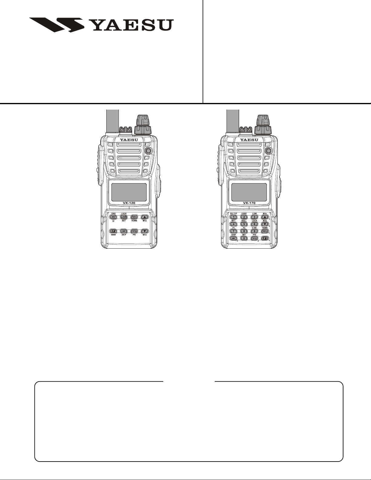
VX-120 VX-170
Introduction
This manual provides the technical information necessary for servicing the VX-120/-170 VHF FM Transceiver.
Servicing this equipment requires expertise in handing surface-mount chip components. Attempts by non-qualified
persons to service this equipment may result in permanent damage not covered by the warranty, and may be illegal in
some countries.
Two PCB layout diagrams are provided for each double-sided board in this transceiver. Each side of the board is
referred to by the type of the majority of components installed on that side (“Side A” or “Side B”). In most cases one
side has only chip components (surface-mount devices), and the other has either a mixture of both chip and leaded
components (trimmers, coils, electrolytic capacitors, ICs, etc.), or leaded components only.
While we believe the information in this manual to be correct, VERTEX STANDARD assumes no liability for damage
that may occur as a result of typographical or other errors that may be present. Your cooperation in pointing out any
inconsistencies in the technical information would be appreciated.
Contents
Specifications ....................................................................................................................................................................2
Exploded View & Miscellaneous Parts .......................................................................................................................3
Block Diagram ..................................................................................................................................................................5
Circuit Description .......................................................................................................................................................... 7
Alignment ..........................................................................................................................................................................9
Board Units (Schematics, Layouts & Parts)
Main Unit................................................................................................................................................................... 13
FTD-7 DTMF Paging Unit (Option) ....................................................................................................................... 29
1

Specifications
General
Frequency Ranges: RX 137 - 174 MHz
TX 144 - 146 (148) MHz
Channel Steps: 5/10/12.5/15/20/25/50/100 kHz
Frequency Stability: ±5 ppm @ 14° to 140° F (–10° to +60° C)
Repeater Shift: ±600 kHz
Emission Type: F2 , F3
Antenna Impedance: 50 Ω
Supply Voltage: Nominal: 7.2 V DC
(Negative Ground) Operating: 6.0 ~ 16.0 V DC (EXT DC Jack)
11.0 ~ 16.0 V DC (EXT DC Jack with Charging)
Current Consumption: 125 mA (Receive, 200 mW output)
(Approx. @7.2 V) 45 mA (Standby, Saver Off)
20.5 mA (Standby, Saver On)
8 mA (Auto Power Off)
1.5 A (5 W TX)
Operating Temperature: –4° to 140° F (–20 °C to +60 °C)
Case Size: 2.36” (W) x 4.72” (H) x 1.26” (D) (60 x 120 x 32 mm)
(W/O knob, antenna, & belt clip)
Weight: 13.8 Oz (390 g) with FNB-83, antenna, and belt clip
Transmitter
RF Power Output: 5.0 W (High) / 2.0 W (Middle) / 0.5 W (Low) (@7.2 V)
Modulation Type: Variable Reactance F2D, F3E
Maximum Deviation: ±5.0 kHz (F2D, F3E)
Spurious Emission: At least 60 dB down (@ High and Middle power)
At least 40 dB down (@ Low power)
Microphone Impedance:2 kΩ
Receiver
Circuit Type: Double-Conversion Superheterodyne
Intermediate Frequencies: 1st: 21.7 MHz
2nd: 450 kHz
Sensitivity: 0.2 µV for 12 dB SINAD (137-140 MHz)
0.16 µV for 12 dB SINAD (140-150 MHz)
0.2 µV for 12 dB SINAD (150-174 MHz)
Selectivity: 12 kHz/35 kHz (–6 dB /–60 dB)
AF Output: 700 mW @ 16 Ω for 10 % THD (Internal Speaker)
(@ 7.5 V) 400 mW @ 8 Ω for 10 % THD (EXT SP Jack)
Specifications are subject to change without notice, and are guaranteed within the 144 MHz amateur band only. Frequency ranges will vary according to transceiver version; check with your dealer.
2
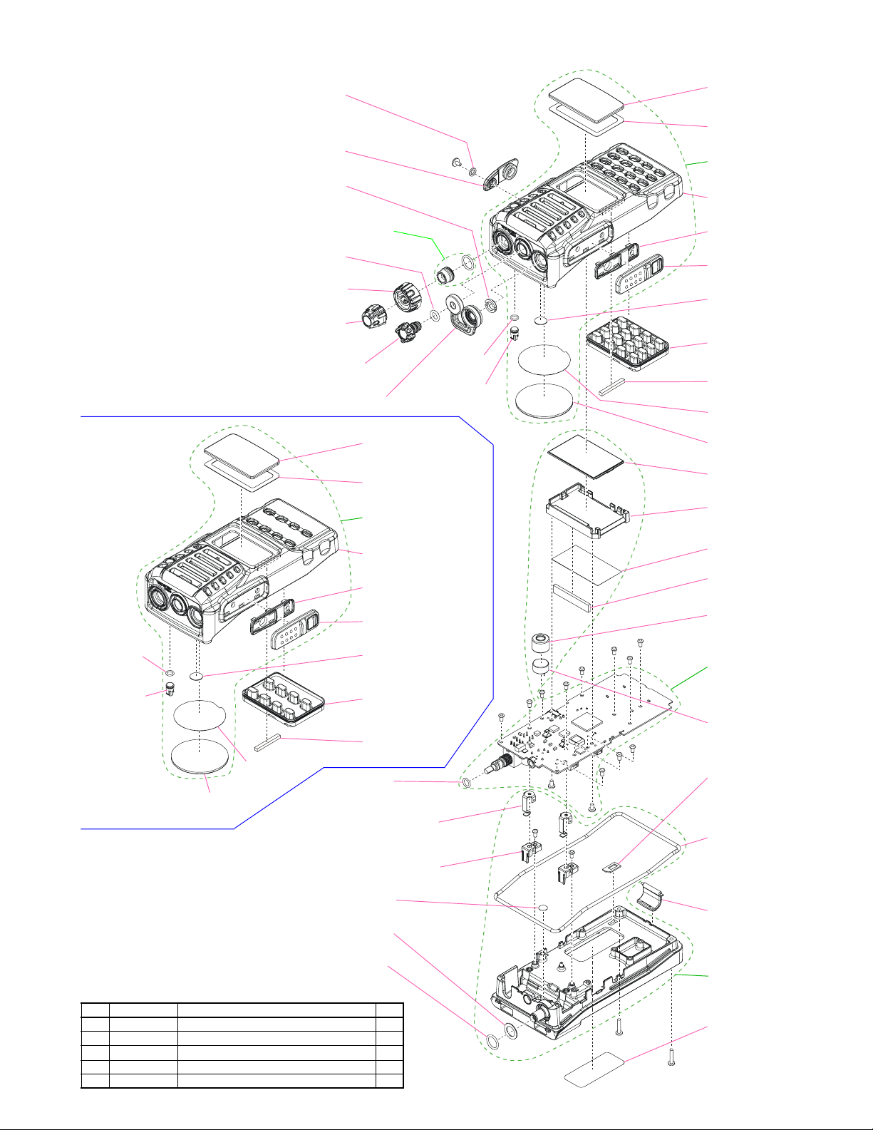
Exploded View & Miscellaneous Parts
VX-170
RA0304300
WASHER
RA0577600
EXT CAP
RA057840A
RING NUT
RA0478500
SPECIAL NUT ASSY
RA0467600
O RING
RA0577800
KNOB
RA0577700
KNOB
RA0577900
KNOB SCREW
RA0578000
RUBBER PACKING
VX-120
RA0401600
O RING
RA057720A
LIGHT GUIDE
RA0557900
SP NET
M4090168
SPEAKER
Non-designated parts are available
only as part of a designated assembly.
Ref.
VXSTD P/N
U24110002
U07240202
U9900068
U9900136
U9900035
TAPTITE SCREW M2X4NI#3
SPECIAL SCREW M2X2.35 4050
TAPTITE SCREW M2X10NI
TAPTITE SCREW M2X3 #1
PAN HEAD SCREW M2X4NI#2
Description
RA057720A
LIGHT GUIDE
RA072170
WINDOW (VX-120)
RA0576900
DOUBLE FACE
RA0721500
PANEL ASSY (VX-120)
RA0721600
PANEL (VX-120)
RA0577100
HOLDER
RA057700A
RUBBER KNOB
RA0434100
SHEET
RA0721800
RUBBER KNOB
RA0607200
SHEET PORON
RA0426900
O RING
RA0577400 (x2 pcs)
TERMINAL
RA057730A (x2 pcs)
SPACER
RA0337300
SHEET
RA0578300
WASHER
S2000056
O RING
Qty.
11
1
2
2
2
RA0401600
O RING
RA0701100
WINDOW (VX-170)
RA0576900
DOUBLE FACE
RA0709200
PANEL ASSY (VX-170)
RA0701000
PANEL (VX-170)
RA0577100
HOLDER
RA057700A
RUBBER KNOB
RA0434100
SHEET
RA0700900
RUBBER KNOB
RA0607200
SHEET PORON
RA0557900
SP NET
M4090168
SPEAKER
G6090166
LCD
RA058040A
LIGHT GUIDE
RA0580500
REFLECTOR SHEET
RA0580700
INTER CONNECTOR
RA0578200
MIC HOLDER RUBBER
MAIN-Unit
M3290029
MIC. ELEMENT
RA069860A
SPACER
RA061740A
RUBBER PACKING
RA0123500
LATCH NAIL
CP8220001
REAR CASE ASSY
RA070930A
MASK SHEET
3

Exploded View & Miscellaneous Parts
Note
4
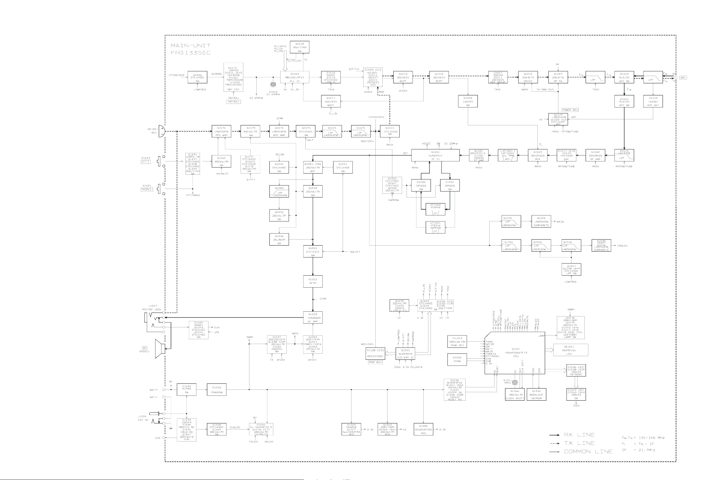
Block Diagram
5

Block Diagram
Note
6

Circuit Description
Receive Signal Path
Incoming RF signal is from the antenna jack is delivered
to the Main Unit and passed through the low-pass filter
network, antenna switching diode D1003 and D1004 (both
RLS135), and low-pass filter network to the RF amplifier
Q1022 (3SK296ZQ). The amplified RF signal is passed
through band-pass filtered again by varactor-tuned bandpass filter consisting of coils L1024, L1025, and L1026, and
diodes D1017, D1018, and D1019 (all HVC350B), then applied to the 1st mixer Q1023 (3SK296ZQ) along with the
first local signal from the PLL circuit.
The first local signal is generated between 115.3 MHz and
152.3 MHz by the VCO, which consists of Q1014
(2SC5005) and varactor diodes D1009, D1010 (both
HVC365) and D1011 (HSC277) according to the receiving frequency.
IF and Audio Circuits
The 21.7 MHz first IF signal is applied to the monolithic
crystal filters XF1001 and XF1002 which strip away unwanted mixer products, and the IF signal is applied to the
first IF amplifier Q1024 (2SC4915). The amplified first IF
signal is then delivered to the FM IF subsystem IC Q1004
(NJM2591V), which contains the second mixer, limiter amplifier, noise amplifier, and FM detector.
The second local signal is generated by 21.25 MHz crystal
X1002, produces the 450 kHz second IF signal when mixed
with first IF signal within Q1004 (NJM2591V).
The 450 kHz second IF signal is applied to the ceramic
filter CF1001 or CF1002 which strip away unwanted mixer products to the ceramic discriminator CD1001 which
removes any amplitude variations in the 450 kHz IF signal before detection of speech.
The detected audio from the Q1004 (NJM2591V) is applied to a band-pass filter consisting of Q1081 and Q1082
(both 2SC4617), then passes through the audio mute gate
Q1052 (2SC4617) and Q1045 (DTC144EE).
The audio signal is passed through the audio VR which
adjusts the audio sensitivity to compensate for audio level variations, then delivered to the audio amplifier Q1008
(TDA2822D).
Squelch Control
When no carrier received, noise at the output of the detector stage in Q1004 (NJM2591V) is applied to pin 49 of
main CPU Q1001 (HD64F2266TF13), which compares the
squelch threshold level to that which set by the SQL knob.
While no carrier is received, pin 71 of Q1001
(HD64F2266TF13) remains “low,” to disable audio output from the speaker.
Transmit Signal Path
The speech signal from the microphone is amplified by
Q1074 (LM2902PWR). The amplified speech signal is sub-
jected to the low-pass filter network Q1074 (LM2902PWR)
and deviation controller Q1075 (DTC144EE).
VHF Transmit Signal Path
The adjusted speech signal from Q1075 (DTC144EE) is
delivered to VCO Q1014 (2SC5005) which frequency
modulates the transmitting VCO made up of D1010
(HVC365).
The modulated transmit signal passes through buffer
amplifier Q1013 and Q1012 (both 2SC5005).
The transmit signal applied to the Pre-Drive amplifier
Q1011 (2SC5005) and Drive amplifier Q1010 (2SK3074),
then finally amplified by Power amplifier Q1009
(2SK3476) up to 5 Watts. This two stages (Q1010 and
Q1009) power amplifier’s gain is controlled by the APC
circuit.
The 5 Watts RF signal passes through low-pass filter network, antenna switch D1003 (RLS135), and another low-
pass filter network, and then deliver to the ANT jack.
Tx APC Circuit
A portion of the Power amplifier output is rectified by
D1002 (1SS321), then delivered to APC Q1019
(LM2904PWR), Q1020 and Q1021 (both DTC144EE), as a
DC voltage which is proportional to the output level of
the power amplifier.
The APC Q1019 (LM2904PWR) is compared the rectified
DC voltage from the power amplifier and the reference
voltage from the main CPU Q1001 (HD64F2266TF13), to
produce a control voltage, which regulates supply voltage to the Drive amplifier Q1010 (2SK3074) and Power
amplifier Q1009 (2SK3476), so as to maintain stable output power under varying antenna loading condition.
PLL
A portion of the output from the VCO Q1014 (2SC5005),
passes through the buffer amplifier Q1017 (2SC5005),
then delivered to the programmable divider section of the
PLL IC Q1003 (MB15A01PFV1), which divided accord-
ing to the frequency dividing data that is associated with
the setting frequency input from the main CPU Q1001
(HD64F2266TF13). It is then sent to the phase comparator.
The 21.25 MHz frequency of the reference oscillator circuit made up of X1002 is divided by the reference frequency divider section of Q1003 (MB15A01PFV1) into 4250 or
3400 parts to become 5 kHz or 6.25 kHz comparative ref-
7

Circuit Description
erence frequencies, which are utilized by the phase comparator.
The phase comparator section of Q1003 (MB15A01PFV1)
compares the phase between the frequency-divided oscillation frequency of the VCO circuit and comparative
frequency and its output is a pulse corresponding to the
phase difference. This pulse is integrated by the charge
pump and loop filter of D1012 (DA221) and Q1016
(DTC144EE) into a control voltage (VCV) to control the
oscillation frequency of the VCO.
8

Alignment
Introduction
The VX-120/-170 is carefully aligned at the factory for the
specified performance across the amateur band. Realignment should therefore not be necessary except in the event
of a component failure. Only an authorized Vertex Standard representative should perform all component replacement and service, or the warranty policy may be void.
The following procedures cover the adjustments that are
not normally required once the transceiver has left the factory. However, if damage occurs and some parts subsequently are replaced, realignment may be required. If a
sudden problem occurs during normal operation, it is likely due to component failure; realignment should not be
done until after the faulty component has been replaced.
We recommend that servicing be performed only by authorized Vertex Standard service technicians who are experienced with the circuitry and fully equipped for repair
and alignment. If a fault is suspected, contact the dealer
from whom the transceiver was purchased for instructions
regarding repair. Authorized Vertex Standard service technicians realign all circuits and make complete performance
checks to ensure compliance with factory specifications
after replacing any faulty components.
Those who do undertake any of the following alignments
are cautioned to proceed at their own risk. Problems
caused by unauthorized attempts at realignment are not
covered by the warranty policy. Also, Vertex Standard
reserves the right to change circuits and alignment procedures in the interest of improved performance, without
notifying owners.
Under no circumstances should any alignment be attempted unless the normal function and operation of the transceiver are clearly understood, the cause of the malfunction has been clearly pinpointed and any faulty components replaced, and realignment determined to be absolutely necessary.
Required Test Equipment
The following test equipment (and familiarity with its use)
is necessary for complete realignment. Correction of problems caused by misalignment resulting from use of improper test equipment is not covered under the warranty
policy. While most steps do not require all of the equipment listed, the interactions of some adjustments may require that more complex adjustments be performed afterwards.
Do not attempt to perform only a single step unless it is
clearly isolated electrically from all other steps. Have all
test equipment ready before beginning and, follow all of
the steps in a section in the order presented.
RF Signal Generator with calibrated output level at 200
MHz
Deviation Meter (linear detector)
In-line Wattmeter with 5% accuracy at 200 MHz
50-Ohm 10-W RF Dummy Load
8-Ohm AF Dummy Load
Regulated DC Power Supply adjustable from 6 to 15
VDC, 2A
Frequency Counter: 0.2-ppm accuracy at 200 MHz
AF Signal Generator
AC Voltmeter
DC Voltmeter: high impedance
VHF Sampling Coupler
SINAD Meter
Alignment Preparation & Precautions
A 50-Ohm RF load and in-line wattmeter must be connected to the main antenna jack in all procedures that call
for transmission; alignment is not possible with an antenna. After completing one step, read the next step to see if
the same test equipment is required. If not, remove the
test equipment (except dummy load and wattmeter, if
connected) before proceeding.
Correct alignment requires that the ambient temperature
be the same as that of the transceiver and test equipment,
and that this temperature be held constant between 68 ~
86° F (20° ~ 30° C). When the transceiver is brought into
the shop from hot or cold air, it should be allowed some
time to come to room temperature before alignment.
Whenever possible, alignments should be made with oscillator shields and circuit boards firmly affixed in place.
Also, the test equipment must be thoroughly warmed up
before beginning.
Note: Signal levels in dB referred to in the alignment pro-
cedure are based on 0dBµ = 0.5µV.
9
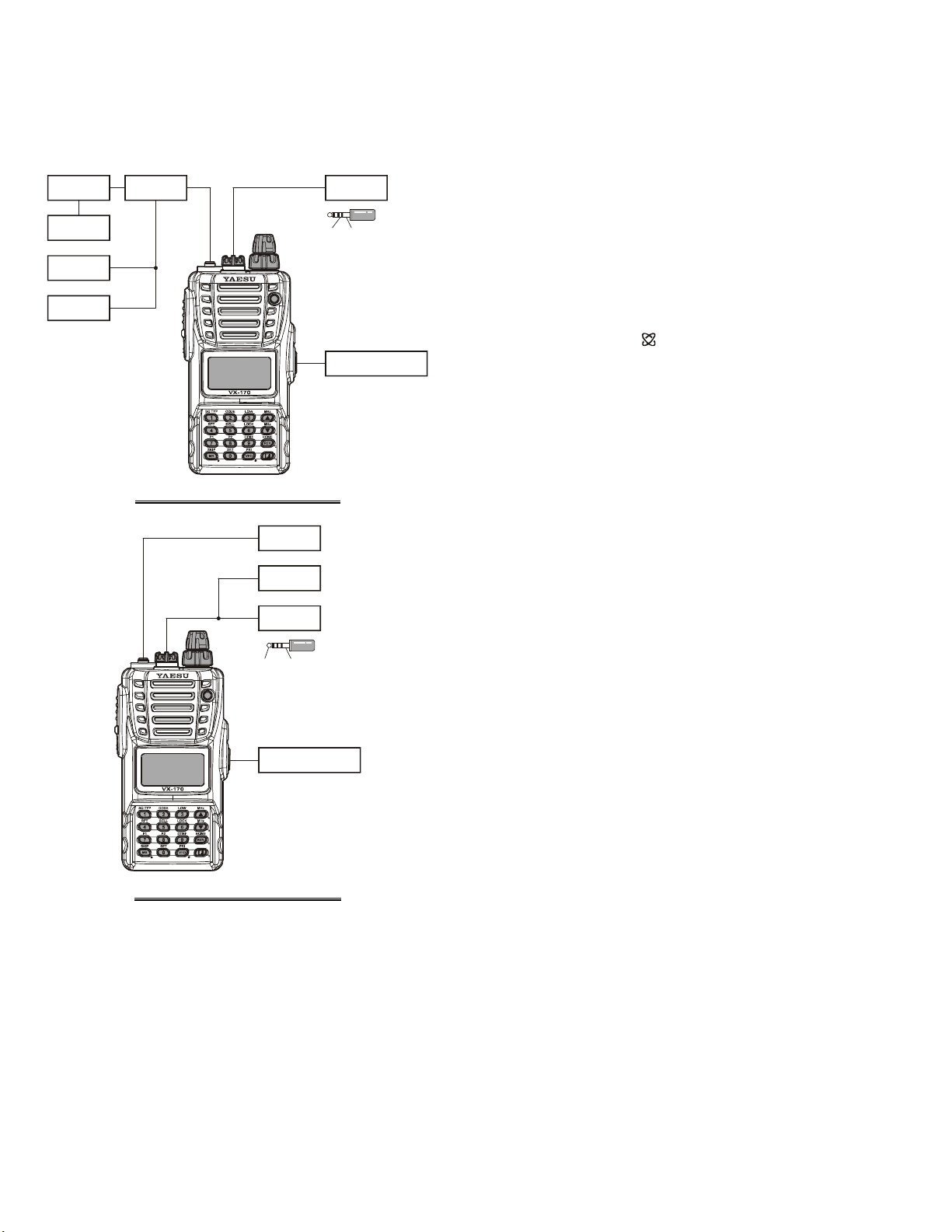
Alignment
Test Setup
Set up the test equipment as shown below for transceiver
alignment.
Inline
Wattmeter
Ω
50
Dummy Load
Frequency
Counte r
Frequency
Counte r
RF Sampling
Coupl er
“TX SECTION” ALIGNMENT SETUP
RF Signal
Generator
Ω
8
Dummy Load
SINAD
Meter
SP GND
AF Signal
Generator
MIC GND
9.9 V DC
Regulated Power Supply
Entering the Alignment Mode
Alignment of the VX-120/-170 is performed using a front
panel software-based procedure. To perform alignment
of the transceiver, it must first be placed in the “Alignment Mode,” in which the adjustments will be made and
then stored into memory.
To enter the Alignment mode:
1. Press and hold in the PTT and MONI switches turning
the radio on. Once the radio is on, release these two
switches.
2. Press the keypad in the following sequence:
VX-120:[WX(EMG
[
REV(HOME)] [(MHz)] [(MHz
) ]
[LOW(LOCK)SET]
)]
VX-170:[(MHz)] [0(SET)] [2(CODE)]
[2(
CODE)] [MR(SKIP
)]
3. Press the [F] key to cause “A0 REF.xxx” to appear on
the display for five seconds, this signifies that the transceiver is now in the “Alignment Mode.”
PLL Reference Frequency
1. Tune the frequency to 145.050 MHz, then set the transmit power level to “LOW.”
2. Press the [F] key, then press the [MR(SKIP)] key to set
the alignment parameter to “A0 REF.xxx,” if needed.
3. With in five second of appearing the “A0 REF.xxx” on
the display, press the PTT switch to activate the transmitter, adjust the DIAL knob so that the counter frequency reading is 145.050 MHz (±100 Hz).
10
7.5 V D C
Regulated Power Supply
“RX SECTION” ALIGNMENT SETUP
 Loading...